CN102047268A - Method of reducing noise in a signal received in a contactless card interrogator and a circuit for performing said method - Google Patents
Method of reducing noise in a signal received in a contactless card interrogator and a circuit for performing said methodDownload PDFInfo
- Publication number
- CN102047268A CN102047268ACN2008801295366ACN200880129536ACN102047268ACN 102047268 ACN102047268 ACN 102047268ACN 2008801295366 ACN2008801295366 ACN 2008801295366ACN 200880129536 ACN200880129536 ACN 200880129536ACN 102047268 ACN102047268 ACN 102047268A
- Authority
- CN
- China
- Prior art keywords
- signal
- receiver
- transmitter
- output
- output signal
- Prior art date
- Legal status (The legal status is an assumption and is not a legal conclusion. Google has not performed a legal analysis and makes no representation as to the accuracy of the status listed.)
- Pending
Links
Images


Classifications
- G—PHYSICS
- G06—COMPUTING OR CALCULATING; COUNTING
- G06K—GRAPHICAL DATA READING; PRESENTATION OF DATA; RECORD CARRIERS; HANDLING RECORD CARRIERS
- G06K7/00—Methods or arrangements for sensing record carriers, e.g. for reading patterns
- G06K7/0008—General problems related to the reading of electronic memory record carriers, independent of its reading method, e.g. power transfer
Landscapes
- Engineering & Computer Science (AREA)
- Artificial Intelligence (AREA)
- Computer Vision & Pattern Recognition (AREA)
- Physics & Mathematics (AREA)
- General Physics & Mathematics (AREA)
- Theoretical Computer Science (AREA)
- Near-Field Transmission Systems (AREA)
Abstract
Description
Translated fromChinese技术领域technical field
本发明涉及降低非接触式卡询问器中收到的信号中噪声的方法和电路,其中发射机-接收机模块与询问器发射机和询问器接收机都连接,并且通过结合接收机输入信号与本机振荡器的输出信号或其正交的信号,将所结合的信号传导通过带通滤波器以清除高频噪声分量和直流分量,并且放大它们,来产生两个接收机输出信号,随后更强的一个所述接收机输出信号被选择、数字化和传导到通信控制器,所提议的解决方案主要用于UHF波段中的非接触式卡询问器。The present invention relates to a method and circuit for reducing noise in signals received in a contactless card interrogator, wherein a transmitter-receiver module is connected to both the interrogator transmitter and the interrogator receiver, and by combining the receiver input signal with The output signal of the local oscillator or its quadrature signal, the combined signal is conducted through a band-pass filter to remove high-frequency noise components and DC components, and they are amplified to produce two receiver output signals, which are subsequently updated. Strong one of said receiver output signals is selected, digitized and conducted to a communication controller. The proposed solution is mainly used for contactless card interrogators in the UHF band.
背景技术Background technique
由非接触式卡发射并由询问器天线接收的具有约900MHz频率的UHF波段中收到信号的解调大多数通过结合彼此正交的两个本机振荡器输出信号而进行(US 2006/0186995A1),以便收到的信号被高效地接收,无论在天线范围内它是调幅还是调相。随后,对解调后的信号清除高频噪声分量和直流分量并放大。两个信号中更强的一个被选择、数字化和传导到通信控制器。由于询问器中的耦合电路将发射机连接到天线并且将天线连接到接收机,以及在接收非接触式卡信号时,询问器必须也发射发射机的载波信号,以便向非接触式卡传递供应能流,所以除了其他噪声以外,收到的非接触式卡信号内包含的发射机载波信号的噪声也被传递到询问器接收机。The demodulation of the received signal in the UHF band with a frequency of about 900 MHz transmitted by the contactless card and received by the interrogator antenna is mostly performed by combining two local oscillator output signals in quadrature with each other (US 2006/0186995A1 ) so that the received signal is received efficiently, whether it is amplitude or phase modulated within the range of the antenna. Subsequently, the demodulated signal is cleaned of high-frequency noise components and DC components and amplified. The stronger of the two signals is selected, digitized and routed to the communications controller. Since the coupling circuit in the interrogator connects the transmitter to the antenna and the antenna to the receiver, and when receiving the contactless card signal, the interrogator must also transmit the transmitter's carrier signal in order to deliver the supply to the contactless card. energy flow, so the noise of the transmitter carrier signal contained in the received contactless card signal is passed to the interrogator receiver, among other noises.
接收机的电子线路中固有的噪声在关于其输入来计算时,在所述频率范围内产生每1Hz宽频带5nV的有效电压,但是典型情况下高级信号发生器的噪声是120dBc,意味着在1mW的功率时(在50Ω上)每1Hz宽频带220nV的有效电压。在询问器发射机的输出处所述载波信号的功率范围从100mW至1W。发射机载波信号的噪声是询问器接收机中重要的或者甚至主要的噪声,因为能够以将具有低噪声的方式在所述频率范围内在其中生产的电子线路。The noise inherent in the electronics of a receiver produces an effective voltage of 5nV per 1Hz broadband over the stated frequency range when calculated with respect to its input, but the noise of an advanced signal generator is typically 120dBc, meaning that at 1mW When the power is high (on 50Ω), the effective voltage is 220nV per 1Hz broadband. The power of the carrier signal at the output of the interrogator transmitter ranges from 100mW to 1W. The noise of the transmitter carrier signal is an important or even dominant noise in the interrogator receiver because of the electronics that can be produced therein in said frequency range in such a way that it will have low noise.
不过,对于询问器中的信号接收,这种估计必须改进。发射机载波信号的噪声包括相位噪声和振幅噪声。发射机载波信号的相位噪声对接收机中的噪声没有贡献,因为两个输入混频器级使用同样产生发射机载波信号的同一本机振荡器的彼此正交的两个输出信号。不过,发射机载波信号的振幅噪声对接收机中的噪声有很强的贡献,因此通过所述信号与彼此正交的两个信号中任一个的相位差异确定传递因子。However, for signal reception in the interrogator, this estimate must be refined. The noise of the transmitter carrier signal includes phase noise and amplitude noise. The phase noise of the transmitter carrier signal does not contribute to the noise in the receiver because the two input mixer stages use two output signals in quadrature with each other from the same local oscillator that also generates the transmitter carrier signal. However, the amplitude noise of the transmitter carrier signal makes a strong contribution to the noise in the receiver, so the transfer factor is determined by the phase difference between said signal and either of the two signals in quadrature to each other.
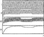
以上陈述利用图1a、图1b、图1c和图1d中表示的仿真展示。所述图的每一幅都在窗口I中表示彼此正交的两个本机振荡器输出信号之一,在窗口II中表示询问器接收机的输入信号,在窗口III中表示询问器混频器级输出的信号,在窗口IV中表示从窗口III中清除了高频噪声分量后的信号。The above statement is demonstrated using the simulations presented in Figures 1a, 1b, 1c and 1d. Each of said figures shows in window I one of two local oscillator output signals in quadrature to each other, in window II the input signal to the interrogator receiver, and in window III the interrogator mixing frequency The output signal of the amplifier stage, in the window IV, represents the signal after the high-frequency noise component has been removed from the window III.
询问器接收机的输入信号与彼此正交的两个本机振荡器输出信号之一在图1a中表示为同相;窗口IV中清除后的振幅解调的信号证明振幅解调产生有效的接收信号。在图1b中,询问器接收机的输入信号与相位彼此正交的两个本机振荡器输出信号的第二个彼此正交;窗口IV中清除后的振幅解调的信号证明振幅解调在这种情况下未产生满意的接收信号。The input signal to the interrogator receiver and one of the two local oscillator output signals in quadrature to each other are shown in phase in Figure 1a; the amplitude demodulated signal after clearing in window IV demonstrates that the amplitude demodulation produces a valid received signal . In Figure 1b, the input signal to the interrogator receiver is in quadrature with the second of two local oscillator output signals that are in phase quadrature with each other; the amplitude-demodulated signal after clearing in window IV demonstrates that the amplitude demodulation was at In this case a satisfactory received signal is not produced.
图1c和图1d表示询问器接收机输入信号的相位解调结果,该信号以具有5MHz频率的信号调相,对于将其与彼此正交的两个本机振荡器输出信号的第一个结合的情况,该第一信号与输入信号正交,或者对于将其与彼此正交的两个本机振荡器输出信号的第二个结合的情况,该第二信号关于输入信号同相。Figures 1c and 1d show the results of phase demodulation of the interrogator receiver input signal phase-modulated with a signal having a frequency of 5 MHz, for the first combination of two local oscillator output signals in quadrature with each other In the case of , this first signal is in quadrature with the input signal, or in the case of combining it with the second of two local oscillator output signals in quadrature with each other, this second signal is in phase with respect to the input signal.
发明内容Contents of the invention
本发明要解决的技术问题是提出这样的方法和这样的电路,利用它无延迟地确定询问器接收机输入信号内的振幅噪声的主要部分被并随后从询问器已经从非接触式卡收到的信号中减去。The technical problem to be solved by the present invention is to propose such a method and such a circuit with which it can be determined without delay that the main part of the amplitude noise in the input signal of the interrogator receiver has been received by the interrogator and subsequently received from the contactless card by the interrogator subtracted from the signal.
本发明的方法和本发明的电路解决了这样的技术问题,其特征分别在于第一权利要求的特征部分的特征和第九权利要求的特征部分的特征,本方法和本电路的实施例的若干变型的特征由若干从属权利要求描述。This technical problem is solved by the method of the invention and the circuit of the invention, which are characterized by the characterizing features of the first claim and the characterizing parts of the ninth claim respectively, several embodiments of the method and of the circuit Variants are characterized by several dependent claims.
用于降低非接触式卡询问器中收到的信号中噪声的本发明的所述方法和所述电路的优点在于,询问器发射机的振幅噪声在通信控制器的输出信号中不再出现,从而显著改进了所述输出信号的信噪比。The advantage of said method and said circuit of the invention for reducing noise in a signal received in a contactless card interrogator is that the amplitude noise of the interrogator transmitter no longer appears in the output signal of the communication controller, The signal-to-noise ratio of the output signal is thereby significantly improved.
附图说明Description of drawings
现在将详细公开本发明,方式为对本发明的方法和电路的若干实施例的介绍以及参考以下附图,其中:The invention will now be disclosed in detail by way of a description of several embodiments of the method and circuit of the invention and with reference to the following drawings in which:
图2和图3本发明的电路实施例的变型,用于降低非接触式卡询问器中收到的信号中的噪声。Figures 2 and 3 are variants of circuit embodiments of the invention for reducing noise in signals received in a contactless card interrogator.
具体实施方式Detailed ways
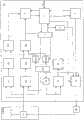
用于降低收到的信号中噪声的本发明的方法在非接触式卡询问器中执行,其中发射机-接收机模块TRM;TRM’都与询问器发射机和询问器接收机连接(图2和图3)。询问器本机振荡器LO产生几个输出信号,全部具有相同的频率;第一信号是发射机输出信号的载波信号。接收机输入信号在两条通道并行处理。通过结合接收机输入信号与本机振荡器LO的第二个输出信号,传导所结合的信号通过带通滤波器321,在此清除直流分量并有力地减少了一部分高频噪声分量,并且放大它,来产生第一接收机输出信号。通过结合接收机输入信号和与本机振荡器LO的第二输出信号正交的本机振荡器LO的第三输出信号,传导所结合的信号通过带通滤波器322并且放大它,来产生第二接收机输出信号。选择第一和第二接收机输出信号中的较强的一个并数字化。结果信号然后被传导到通信控制器1,它接收输入信号、发送输出信号ios并且与发射机数模转换器2通信。The inventive method for reducing noise in the received signal is implemented in a contactless card interrogator, where the transmitter-receiver module TRM; TRM' is connected to both the interrogator transmitter and the interrogator receiver (Fig. 2 and Figure 3). The interrogator local oscillator LO generates several output signals, all of the same frequency; the first signal is the carrier signal of the transmitter output signal. Receiver input signals are processed in parallel on two channels. By combining the receiver input signal with the second output signal of the local oscillator LO, the combined signal is passed through a
用于降低非接触式卡询问器中收到的信号中噪声的本发明的方法的特征在于以下步骤。The inventive method for reducing noise in a signal received in a contactless card interrogator is characterized by the following steps.
产生发射机的标定输出信号,因为本机振荡器LO的第一输出信号经过以导频信号弱调幅——1%振幅的量级。导频信号的频率应当等于非接触式卡编码数据的频率。A nominal output signal of the transmitter is generated because the first output signal of the local oscillator LO is weakly amplitude modulated with the pilot signal - on the order of 1% amplitude. The frequency of the pilot signal should be equal to the frequency of the contactless card encoded data.
在询问器中产生接收机参考信号,方式为结合发射机的标定输出信号与某信号,它的载波信号具有的频率等于本机振荡器LO输出信号的频率,传导所结合的信号通过带通滤波器42并且放大它。The receiver reference signal is generated in the interrogator by combining the calibrated output signal of the transmitter with a signal whose carrier signal has a frequency equal to the frequency of the local oscillator LO output signal, and conducting the combined signal through
这里,所述信号可以是本机振荡器LO的第四输出信号,其相位以适当的方式设置,使得在辅助混频器级41的输入处其相位等于辅助混频器级41的输入处发射机的标定输出信号的相位,并且实现振幅解调的最大效果;所述信号也可以简单地为具有改变振幅的发射机的标定输出信号。Here, the signal may be the fourth output signal of the local oscillator LO, the phase of which is set in a suitable manner so that at the input of the
然后,通过分别从第一和第二接收机输出信号中减去接收机参考信号而清除第一和第二接收机输出信号,接收机参考信号已经被标定因子衰减并已经得到了第一或第二接收机输出信号的标定极性。The first and second receiver output signals are then cleared by subtracting the receiver reference signal, which has been attenuated by the scaling factor and which has yielded the first or second receiver output signal, respectively, from the first and second receiver output signals. 2. Calibration polarity of receiver output signal.
对于两个接收机输出信号的每一个,接收机参考信号的衰减因子和极性都不时地或者每当天线的条件或天线周围的空间已经显著改变时被重新标定。For each of the two receiver output signals, the attenuation factor and polarity of the receiver reference signal are recalibrated from time to time or whenever the conditions of the antenna or the space around the antenna have changed significantly.
对于两个接收机输出信号的每一个,所述接收机参考信号的衰减因子和它的极性进行标定的步骤都包含在以下指令中。The steps of calibrating the attenuation factor of the receiver reference signal and its polarity for each of the two receiver output signals are included in the following instructions.
对于两个接收机输出信号的每一个,所述接收机参考信号的衰减因子和它的极性被确定和设置为,在标定后的数值对,使第一以及第二清除后的接收机输出信号具有最小的振幅。For each of the two receiver output signals, the attenuation factor of the receiver reference signal and its polarity are determined and set as, after scaling, the value pairs such that the first and second cleared receiver outputs The signal has the smallest amplitude.
降低所收到信号中噪声的本发明的方法在配备了发射机-接收机模块TRM或TRM’的非接触式卡询问器中执行。The inventive method of reducing noise in the received signal is implemented in a contactless card interrogator equipped with a transmitter-receiver module TRM or TRM'.
发射机-接收机模块TRM包括耦合电路CC以及发射和接收天线A(图2)。这里为分离所收到信号和发射机载波信号所提供的定向耦合器、环行器或分立电路可以用作耦合电路CC。The transmitter-receiver module TRM comprises a coupling circuit CC and a transmitting and receiving antenna A (Fig. 2). A directional coupler, a circulator or a discrete circuit provided here for separating the received signal and the transmitter carrier signal can be used as coupling circuit CC.
发射机-接收机模块TRM’包括连接到询问器发射机输出的发射天线At,以及连接到询问器接收机输入的接收天线Ar(图3)。The transmitter-receiver module TRM' comprises a transmit antenna At connected to the output of the interrogator transmitter, and a receive antenna Ar connected to the input of the interrogator receiver (Fig. 3).
定向耦合器例如在从天线向询问器接收机的方向,衰减发射机的输出信号比从非接触式卡收到的信号强有力得多。从而在询问器接收机的输入信号中来自发射机输出信号的噪声的贡献以这种方式降低了20dB到30dB,然而这种贡献仍然占优势。A directional coupler, for example in the direction from the antenna to the interrogator receiver, attenuates the output signal of the transmitter much stronger than the signal received from the contactless card. The contribution of noise from the transmitter output signal in the input signal to the interrogator receiver is thus reduced by 20 dB to 30 dB in this way, however this contribution still predominates.
降低所收到信号中噪声的本发明的电路被制造在非接触式卡询问器的芯片IC或IC’上。发射机-接收机模块TRM或TRM’可以在芯片IC或芯片IC’上使用,并都连接到发射机振幅调制器21的输出,通常通过匹配电路MC,并且连接到第一和第二接收机混频器级311、312的第一输入。The circuit of the present invention that reduces noise in the received signal is fabricated on the chip IC or IC' of the contactless card interrogator. A transmitter-receiver module TRM or TRM' can be used on a chip IC or a chip IC' and both are connected to the output of the
本机振荡器LO的第一输出信号作为发射机输出信号的载波信号被传导至发射机振幅调制器21的第一输入。本机振荡器LO的全部输出信号都具有同一频率。来自数模转换器2的调制信号被传导至发射机振幅调制器21的第二输入。A first output signal of the local oscillator LO is conducted to a first input of a
彼此正交的本机振荡器LO的第二和第三输出信号分别被传导至所述第一和第二接收机混频器级311、312的第二输入。The second and third output signals of the local oscillator LO, which are in quadrature with each other, are conducted to second inputs of said first and second
所述第一和第二接收机混频器级311、312的输出信号通过第一和第二带通滤波器和放大器321、322分别被传导至选择-数字化电路3的第一和第二输入。所述选择-数字化电路3连接到通信控制器1。The output signals of said first and second
正如本发明的提议,降低非接触式卡询问器中收到的信号中噪声的电路也配备了辅助混频器级41、辅助带通滤波器和放大器42、用于衰减和极性设置的受控第一和第二电路4AP1、4AP2、第一和第二减法器3S1、3S2、校正电路5以及导频信号发生器6。本发明的电路的特征在于以下连接。As proposed by the present invention, the circuit for reducing noise in the signal received in the contactless card interrogator is also equipped with an
发射机输出信号分接在匹配电路MC的前面或后面,或者甚至在耦合电路CC的后面,并且在需要时甚至可以被衰减,以便不超过辅助混频器级41的输入的动态范围。发射机输出信号被传导至辅助混频器级41的第一输入。向其第二输入传导的信号的载波信号具有本机振荡器LO的输出信号的频率。所述信号或者是本机振荡器LO的第四输出信号,该信号可以通过移相器40传导至辅助混频器级41的第二输入,或者是为了设置发射机输出信号的振幅而通过电路40’供给的发射机输出信号。The transmitter output signal is tapped before or after the matching circuit MC, or even after the coupling circuit CC, and can even be attenuated if necessary, so as not to exceed the dynamic range of the input of the
辅助混频器级41的输出连接到代表辅助带通滤波器和放大器的电路42的输入。包含发射机噪声低频分量的解调后发射机输出信号出现在电路42的输出处。严格地说,解调后的非接触式卡信号也出现在代表辅助带通滤波器和放大器的电路42的输出处,然而与解调后发射机噪声的低频分量相比相当弱。The output of the
辅助带通滤波器和放大器电路42的输出通过第一和第二受控衰减和极性设置电路4AP1、4AP2分别连接到第一和第二减法器3S1、3S2的第二输入。第一和第二带通滤波器和放大器电路321、322的输出分别连接到减法器3S1和减法器3S2的第一输入。The output of the auxiliary bandpass filter and
一方面任一减法器3S1和3S2的输出分别连接到选择-数字化电路3的第一和第二输入,另一方面也分别连接到校正电路5的第一和第二输入。The outputs of any one of the subtractors 3S1 and 3S2 are respectively connected to the first and second inputs of the selection-
校正电路5控制着衰减和极性设置电路4AP1、4AP2,方式为利用来自辅助带通滤波器和放大器电路42输出的接收机参考信号,第一和第二接收机输出信号也分别最优地清除了发射机输出信号振幅解调后噪声的低频分量,接收机参考信号按以下介绍的适当方式缩放。The
校正电路5也控制着导频信号发生器6。导频信号的频率等于非接触式卡进行数据编码的频率。导频信号发生器6的输出连接到询问器发射机振幅调制器21的第二输入,向所述第二输入提供要与本机振荡器LO的第一输出信号结合的调制信号。另外,发射机振幅调制器21还由通信控制器1控制。The
当校正电路5已经触发了导频信号发生器时,它也开始观测第一和第二清除后的接收机输出信号并控制着衰减和极性设置电路4AP1、4AP2的设置,直到它检测出第一和第二清除后的接收机输出信号的最小值。从而标定了本发明的电路。校正电路5冻结这个设置并关闭导频信号发生器6。非接触式卡询问器现在准备运行。When the
因此,本发明的方法和电路显著改进了通信控制器1的输出处信号ios的信噪比。Thus, the method and the circuit of the invention significantly improve the signal-to-noise ratio of the signal ios at the output of the
如果接收天线A;Ar的阻抗改变,或者接收条件由于无线电波的不同反射而显著变化,或者如果非接触式卡信号的频率范围与期望范围不同并在类似的改变后环境中,校正电路5再次触发标定动作。If the impedance of the receiving antenna A; Ar changes, or the receiving conditions change significantly due to different reflections of radio waves, or if the frequency range of the contactless card signal is different from the expected range and in a similar changed environment, the
Claims (18)
Translated fromChineseApplications Claiming Priority (1)
| Application Number | Priority Date | Filing Date | Title |
|---|---|---|---|
| PCT/SI2008/000025WO2009128791A1 (en) | 2008-04-15 | 2008-04-15 | Method for reducing a noise in a signal received in a contactless-card interrogator and a circuit to perform said method |
Publications (1)
| Publication Number | Publication Date |
|---|---|
| CN102047268Atrue CN102047268A (en) | 2011-05-04 |
Family
ID=39639650
Family Applications (1)
| Application Number | Title | Priority Date | Filing Date |
|---|---|---|---|
| CN2008801295366APendingCN102047268A (en) | 2008-04-15 | 2008-04-15 | Method of reducing noise in a signal received in a contactless card interrogator and a circuit for performing said method |
Country Status (4)
| Country | Link |
|---|---|
| US (1) | US8867989B2 (en) |
| EP (1) | EP2266072B8 (en) |
| CN (1) | CN102047268A (en) |
| WO (1) | WO2009128791A1 (en) |
Cited By (1)
| Publication number | Priority date | Publication date | Assignee | Title |
|---|---|---|---|---|
| CN102902939A (en)* | 2012-09-29 | 2013-01-30 | 中国物品编码中心 | Carrier cancellation device |
Families Citing this family (3)
| Publication number | Priority date | Publication date | Assignee | Title |
|---|---|---|---|---|
| US8798198B2 (en) | 2011-08-31 | 2014-08-05 | Apple Inc. | Calibration systems for wireless electronic devices |
| SI23939A (en) | 2011-11-30 | 2013-05-31 | Ids D.O.O. | A method for reducing the amplitude noise in receiving signal in RFID transponder |
| GB2518257A (en)* | 2013-09-13 | 2015-03-18 | Vodafone Ip Licensing Ltd | Methods and systems for operating a secure mobile device |
Citations (3)
| Publication number | Priority date | Publication date | Assignee | Title |
|---|---|---|---|---|
| US20060186995A1 (en)* | 2005-02-22 | 2006-08-24 | Jiangfeng Wu | Multi-protocol radio frequency identification reader tranceiver |
| CN1948977A (en)* | 2005-10-11 | 2007-04-18 | 上海华虹集成电路有限责任公司 | Non-contacting intelligent card noise detecting method and detecting circuit thereof |
| CN101014964A (en)* | 2003-12-19 | 2007-08-08 | 讯宝科技公司 | Single chip, noise-resistant, one-dimensional, cmos sensor for target imaging |
- 2008
- 2008-04-15CNCN2008801295366Apatent/CN102047268A/enactivePending
- 2008-04-15USUS12/736,504patent/US8867989B2/ennot_activeExpired - Fee Related
- 2008-04-15EPEP08741975.0Apatent/EP2266072B8/ennot_activeNot-in-force
- 2008-04-15WOPCT/SI2008/000025patent/WO2009128791A1/enactiveApplication Filing
Patent Citations (3)
| Publication number | Priority date | Publication date | Assignee | Title |
|---|---|---|---|---|
| CN101014964A (en)* | 2003-12-19 | 2007-08-08 | 讯宝科技公司 | Single chip, noise-resistant, one-dimensional, cmos sensor for target imaging |
| US20060186995A1 (en)* | 2005-02-22 | 2006-08-24 | Jiangfeng Wu | Multi-protocol radio frequency identification reader tranceiver |
| CN1948977A (en)* | 2005-10-11 | 2007-04-18 | 上海华虹集成电路有限责任公司 | Non-contacting intelligent card noise detecting method and detecting circuit thereof |
Cited By (2)
| Publication number | Priority date | Publication date | Assignee | Title |
|---|---|---|---|---|
| CN102902939A (en)* | 2012-09-29 | 2013-01-30 | 中国物品编码中心 | Carrier cancellation device |
| CN102902939B (en)* | 2012-09-29 | 2015-07-22 | 中国物品编码中心 | Carrier cancellation device |
Also Published As
| Publication number | Publication date |
|---|---|
| EP2266072A1 (en) | 2010-12-29 |
| US20110032080A1 (en) | 2011-02-10 |
| EP2266072B1 (en) | 2013-02-13 |
| WO2009128791A1 (en) | 2009-10-22 |
| EP2266072B8 (en) | 2013-04-17 |
| US8867989B2 (en) | 2014-10-21 |
Similar Documents
| Publication | Publication Date | Title |
|---|---|---|
| US7986931B2 (en) | RFID reader and circuit and method for echo cancellation thereof | |
| US8385235B2 (en) | Full division duplex system and a leakage cancellation method | |
| KR100731227B1 (en) | Rfid transceiver device | |
| US10444326B2 (en) | FMCW radar | |
| US7412217B2 (en) | Transceiver with interference signal rejection, and method for interference signal rejection | |
| TW200901644A (en) | Wireless receiver with notch filter to reduce effects of transmit signal leakage | |
| US11112486B2 (en) | Radar apparatus | |
| CN102047268A (en) | Method of reducing noise in a signal received in a contactless card interrogator and a circuit for performing said method | |
| CN110896315A (en) | Wireless radio frequency communication system | |
| EP4254788A3 (en) | Radio frequency front end for a full duplex or half duplex transceiver | |
| JP4842342B2 (en) | Radio transmission / reception device and method for measuring transmission power of radio transmission / reception device | |
| JP2010109462A (en) | Directional coupler, and transmitting and receiving apparatus | |
| US20010051507A1 (en) | Direct conversion receiver and transceiver | |
| WO2017130519A1 (en) | High-frequency front-end circuit and communication device | |
| JP2007215140A (en) | Semiconductor integrated circuit and semiconductor integrated circuit for radio communication | |
| CN114499562A (en) | High-sensitivity anti-blocking radio frequency receiver front end with impedance mapping function | |
| CN100565565C (en) | Be used to carry out the signal processing circuit of the communication partner device of contactless communication | |
| JP2011239401A (en) | Transmitter receiver capable of removing phase noise | |
| JP4543817B2 (en) | Power line carrier communication equipment | |
| CN105049387A (en) | RFID system backward link carrier interference elimination method | |
| CN106105122B (en) | Processing circuit and signal correction method | |
| KR20080112669A (en) | Leakage Signal Rejection Circuit and Mobile Wireless Reader | |
| US8280336B2 (en) | Apparatus and method for eliminating outband interference signal | |
| CN219065728U (en) | Ultra-high-sensitivity radar radio frequency signal conditioning plate | |
| JP4745054B2 (en) | Radio receiving apparatus and radio communication apparatus |
Legal Events
| Date | Code | Title | Description |
|---|---|---|---|
| C06 | Publication | ||
| PB01 | Publication | ||
| C10 | Entry into substantive examination | ||
| SE01 | Entry into force of request for substantive examination | ||
| ASS | Succession or assignment of patent right | Owner name:IDS MICROCHIP AG Free format text:FORMER OWNER: VINKO KUNC Effective date:20130716 Free format text:FORMER OWNER: ANDREJ VODOPIVEC MAJA ATANASIJEVIC-KUNC ANTON STERN Effective date:20130716 | |
| C41 | Transfer of patent application or patent right or utility model | ||
| TA01 | Transfer of patent application right | Effective date of registration:20130716 Address after:Swiss Wollerau Applicant after:IDS microchip Corporation Address before:Slovenia Ljubljana Applicant before:Venko Kunz Applicant before:Andre Vodopivets Applicant before:Atanasijevic-Kunc Maja Applicant before:Stern Anton | |
| ASS | Succession or assignment of patent right | Owner name:AMS INTERNATIONAL LTD. Free format text:FORMER OWNER: IDS MICROCHIP AG Effective date:20140515 | |
| C41 | Transfer of patent application or patent right or utility model | ||
| TA01 | Transfer of patent application right | Effective date of registration:20140515 Address after:La Perth, Switzerland Applicant after:AMS INTERNATIONAL CO., LTD. Address before:Swiss Wollerau Applicant before:IDS microchip Corporation | |
| AD01 | Patent right deemed abandoned | Effective date of abandoning:20110504 | |
| C20 | Patent right or utility model deemed to be abandoned or is abandoned |