CN102044801B - Electric connector and assembling method - Google Patents
Electric connector and assembling methodDownload PDFInfo
- Publication number
- CN102044801B CN102044801BCN2009103084690ACN200910308469ACN102044801BCN 102044801 BCN102044801 BCN 102044801BCN 2009103084690 ACN2009103084690 ACN 2009103084690ACN 200910308469 ACN200910308469 ACN 200910308469ACN 102044801 BCN102044801 BCN 102044801B
- Authority
- CN
- China
- Prior art keywords
- terminal
- main part
- opening
- insulating body
- terminals
- Prior art date
- Legal status (The legal status is an assumption and is not a legal conclusion. Google has not performed a legal analysis and makes no representation as to the accuracy of the status listed.)
- Expired - Fee Related
Links
Images


Classifications
- H—ELECTRICITY
- H01—ELECTRIC ELEMENTS
- H01R—ELECTRICALLY-CONDUCTIVE CONNECTIONS; STRUCTURAL ASSOCIATIONS OF A PLURALITY OF MUTUALLY-INSULATED ELECTRICAL CONNECTING ELEMENTS; COUPLING DEVICES; CURRENT COLLECTORS
- H01R13/00—Details of coupling devices of the kinds covered by groups H01R12/70 or H01R24/00 - H01R33/00
- H01R13/646—Details of coupling devices of the kinds covered by groups H01R12/70 or H01R24/00 - H01R33/00 specially adapted for high-frequency, e.g. structures providing an impedance match or phase match
- H01R13/6461—Means for preventing cross-talk
- H01R13/6471—Means for preventing cross-talk by special arrangement of ground and signal conductors, e.g. GSGS [Ground-Signal-Ground-Signal]
- H—ELECTRICITY
- H01—ELECTRIC ELEMENTS
- H01R—ELECTRICALLY-CONDUCTIVE CONNECTIONS; STRUCTURAL ASSOCIATIONS OF A PLURALITY OF MUTUALLY-INSULATED ELECTRICAL CONNECTING ELEMENTS; COUPLING DEVICES; CURRENT COLLECTORS
- H01R12/00—Structural associations of a plurality of mutually-insulated electrical connecting elements, specially adapted for printed circuits, e.g. printed circuit boards [PCB], flat or ribbon cables, or like generally planar structures, e.g. terminal strips, terminal blocks; Coupling devices specially adapted for printed circuits, flat or ribbon cables, or like generally planar structures; Terminals specially adapted for contact with, or insertion into, printed circuits, flat or ribbon cables, or like generally planar structures
- H01R12/70—Coupling devices
- H01R12/71—Coupling devices for rigid printing circuits or like structures
- H01R12/712—Coupling devices for rigid printing circuits or like structures co-operating with the surface of the printed circuit or with a coupling device exclusively provided on the surface of the printed circuit
- H—ELECTRICITY
- H01—ELECTRIC ELEMENTS
- H01R—ELECTRICALLY-CONDUCTIVE CONNECTIONS; STRUCTURAL ASSOCIATIONS OF A PLURALITY OF MUTUALLY-INSULATED ELECTRICAL CONNECTING ELEMENTS; COUPLING DEVICES; CURRENT COLLECTORS
- H01R13/00—Details of coupling devices of the kinds covered by groups H01R12/70 or H01R24/00 - H01R33/00
- H01R13/646—Details of coupling devices of the kinds covered by groups H01R12/70 or H01R24/00 - H01R33/00 specially adapted for high-frequency, e.g. structures providing an impedance match or phase match
- H01R13/6473—Impedance matching
- H01R13/6474—Impedance matching by variation of conductive properties, e.g. by dimension variations
- H—ELECTRICITY
- H01—ELECTRIC ELEMENTS
- H01R—ELECTRICALLY-CONDUCTIVE CONNECTIONS; STRUCTURAL ASSOCIATIONS OF A PLURALITY OF MUTUALLY-INSULATED ELECTRICAL CONNECTING ELEMENTS; COUPLING DEVICES; CURRENT COLLECTORS
- H01R13/00—Details of coupling devices of the kinds covered by groups H01R12/70 or H01R24/00 - H01R33/00
- H01R13/46—Bases; Cases
- H01R13/502—Bases; Cases composed of different pieces
- H—ELECTRICITY
- H01—ELECTRIC ELEMENTS
- H01R—ELECTRICALLY-CONDUCTIVE CONNECTIONS; STRUCTURAL ASSOCIATIONS OF A PLURALITY OF MUTUALLY-INSULATED ELECTRICAL CONNECTING ELEMENTS; COUPLING DEVICES; CURRENT COLLECTORS
- H01R2107/00—Four or more poles
- H—ELECTRICITY
- H01—ELECTRIC ELEMENTS
- H01R—ELECTRICALLY-CONDUCTIVE CONNECTIONS; STRUCTURAL ASSOCIATIONS OF A PLURALITY OF MUTUALLY-INSULATED ELECTRICAL CONNECTING ELEMENTS; COUPLING DEVICES; CURRENT COLLECTORS
- H01R43/00—Apparatus or processes specially adapted for manufacturing, assembling, maintaining, or repairing of line connectors or current collectors or for joining electric conductors
- H01R43/20—Apparatus or processes specially adapted for manufacturing, assembling, maintaining, or repairing of line connectors or current collectors or for joining electric conductors for assembling or disassembling contact members with insulating base, case or sleeve
- Y—GENERAL TAGGING OF NEW TECHNOLOGICAL DEVELOPMENTS; GENERAL TAGGING OF CROSS-SECTIONAL TECHNOLOGIES SPANNING OVER SEVERAL SECTIONS OF THE IPC; TECHNICAL SUBJECTS COVERED BY FORMER USPC CROSS-REFERENCE ART COLLECTIONS [XRACs] AND DIGESTS
- Y10—TECHNICAL SUBJECTS COVERED BY FORMER USPC
- Y10T—TECHNICAL SUBJECTS COVERED BY FORMER US CLASSIFICATION
- Y10T29/00—Metal working
- Y10T29/49—Method of mechanical manufacture
- Y10T29/49002—Electrical device making
- Y10T29/49117—Conductor or circuit manufacturing
- Y10T29/49204—Contact or terminal manufacturing
- Y10T29/49208—Contact or terminal manufacturing by assembling plural parts
Landscapes
- Details Of Connecting Devices For Male And Female Coupling (AREA)
Abstract
Translated fromChineseDescription
Translated fromChinese【技术领域】【Technical field】
本发明是有关一种电连接器及其组装方法,尤指一种具有相邻端子的电连接器及其组装方法。The present invention relates to an electrical connector and its assembly method, especially to an electrical connector with adjacent terminals and its assembly method.
【背景技术】【Background technique】
在电子产品中,通常使用电连接器传导电信号,通常电连接器中具有传送高频信号的一对相邻的信号端子,而该相邻信号端子之间会产生特征阻抗,只有在适当的特征阻抗下信号端子传送的高频信号才能稳定传输而不会产生信号失真。该端子间的特征阻抗随着两相邻端子之间的电容增大而减小,而电容与两端子的正对面积成正比。In electronic products, electrical connectors are usually used to conduct electrical signals. Generally, electrical connectors have a pair of adjacent signal terminals that transmit high-frequency signals, and a characteristic impedance will be generated between the adjacent signal terminals. Only when appropriate The high-frequency signal transmitted by the signal terminal under the characteristic impedance can be transmitted stably without signal distortion. The characteristic impedance between the terminals decreases as the capacitance between two adjacent terminals increases, and the capacitance is proportional to the facing area of the two terminals.
在目前的电连接器中,由于端子必须具有足够的宽度以保证端子的强度,故两相邻端子间的正对面积相对较大,使端子间的特征阻抗变小而不利于达到保证高频信号传输的要求,使高频信号传输失真。In the current electrical connectors, since the terminals must have sufficient width to ensure the strength of the terminals, the facing area between two adjacent terminals is relatively large, which makes the characteristic impedance between the terminals smaller and is not conducive to ensuring high frequency Signal transmission requirements distort high-frequency signal transmission.
因此,针对上述问题,有必要提出一种技术方案以解决上述问题。Therefore, in view of the above problems, it is necessary to propose a technical solution to solve the above problems.
【发明内容】【Content of invention】
本发明所要解决的技术问题在于提供一种可增大相邻端子间特征阻抗的电连接器及其组装方便的组装方法。The technical problem to be solved by the present invention is to provide an electrical connector capable of increasing the characteristic impedance between adjacent terminals and a convenient assembly method thereof.
为解决上述问题,本发明电连接器采用如下技术方案:一种电连接器,包括:绝缘本体及收容于绝缘本体内的端子,所述端子包括位于第一排并交替排列的第一端子、第二端子及位于第二排并交替排列的第三端子、第四端子,第一端子与第四端子的结构相同,第二端子与第三端子的结构相同,所述第一端子及第三端子是连接于同一料带上,第二端子及第四端子是连接于同一料带上,第一端子具有第一主体部及自第一主体部延伸的第一接触部,第二端子具有第二主体部及自第二主体部延伸的第二接触部,所述第一主体部与第二主体部相面对,且第一主体部及第二主体部均具有相同的外朝第一方向(A)的第一侧缘及外朝与第一方向相反的第二方向(B)的第二侧缘,所述第一主体部具有位于第二侧缘的第一实体部及位于第一侧缘的第一开口部,所述第一开口部具有位于第一侧缘并贯穿第一主体部的第一开口;第二主体部具有位于第一侧缘的第二实体部及位于第二侧缘的第二开口部,所述第二开口部具有位于第二侧缘并贯穿第二主体部的第二开口,该第一、第二开口错开设置。In order to solve the above problems, the electrical connector of the present invention adopts the following technical solution: an electrical connector, comprising: an insulating body and terminals accommodated in the insulating body, and the terminals include first terminals arranged alternately in the first row, The second terminal, the third terminal and the fourth terminal arranged alternately in the second row, the first terminal and the fourth terminal have the same structure, the second terminal and the third terminal have the same structure, and the first terminal and the third terminal have the same structure. The terminals are connected to the same strip, the second terminal and the fourth terminal are connected to the same strip, the first terminal has a first main body and a first contact portion extending from the first main body, the second terminal has a second Two main body parts and a second contact part extending from the second main body part, the first main body part and the second main body part face each other, and both the first main body part and the second main body part have the same outward first direction The first side edge of (A) and the second side edge facing the second direction (B) opposite to the first direction, the first body part has a first solid part located at the second side edge and a first solid part located at the first The first opening portion of the side edge, the first opening portion has a first opening at the first side edge and passes through the first main body portion; the second main body portion has a second solid portion at the first side edge and a second solid portion at the second The second opening on the side edge, the second opening has a second opening located on the second side edge and passing through the second main body, the first and second openings are arranged in a staggered manner.
与现有技术相比,本发明电连接器具有如下有益效果:所述第一主体部具有位于第二侧缘的第一实体部及位于第一侧缘的第一开口部,所述第一开口部具有位于第一侧缘并贯穿第一主体部的第一开口;第二主体部具有位于第一侧缘的第二实体部及位于第二侧缘的第二开口部,所述第二开口部具有位于第二侧缘并贯穿第二主体部的第二开口,该第一、第二开口错开设置,使相邻的两个端子的主体部产生电容效应的正对面积减少而减少电容,从而增大端子间的特征阻抗以满足高频信号传输的需要,使高频信号可以稳定传输。Compared with the prior art, the electrical connector of the present invention has the following beneficial effects: the first main body portion has a first solid portion located at the second side edge and a first opening portion located at the first side edge, the first The opening portion has a first opening located at the first side edge and passing through the first main body portion; the second main body portion has a second solid portion located at the first side edge and a second opening portion located at the second side edge, the second body portion The opening portion has a second opening located on the second side edge and passing through the second main body portion. The first and second openings are arranged in a staggered manner, so that the facing area of the main body portions of the two adjacent terminals that produce capacitance effects is reduced to reduce capacitance. , so as to increase the characteristic impedance between terminals to meet the needs of high-frequency signal transmission, so that high-frequency signals can be transmitted stably.
为解决上述问题,本发明电连接器的组装方法可采用如下技术方案:一种电连接器的组装方法,其特征在于:该组装方法包括以下步骤,In order to solve the above problems, the assembly method of the electrical connector of the present invention can adopt the following technical solution: an assembly method of the electrical connector, characterized in that: the assembly method includes the following steps,
提供绝缘本体,该绝缘本体具有两排端子槽,每一排端子槽包括交替设置的第一端子槽及第二端子槽;An insulating body is provided, the insulating body has two rows of terminal slots, and each row of terminal slots includes alternately arranged first terminal slots and second terminal slots;
提供第一料带,第一料带连接有第一端子组,所述第一端子组包括并列的第一端子及第三端子,该第一端子及第三端子分别具有主体部、自主体部延伸的接触部及延伸出绝缘本体的焊接部,所述主体部分别具有实体部及开口,将该第一端子组组装入第一端子槽中;A first strip is provided, the first strip is connected with a first terminal group, the first terminal group includes a first terminal and a third terminal arranged side by side, and the first terminal and the third terminal respectively have a main body part and an independent main body part The extended contact part and the welding part extending out of the insulating body, the main body part has a solid part and an opening respectively, and the first terminal is assembled into the first terminal groove;
提供第二料带,第二料带连接有第二端子组,所述第二端子组包括并列的第二端子及第四端子,该第二端子组是由第一端子组旋转180度而成,将该第二端子组组装入第二端子槽中,此时第一端子的开口与第二端子的开口错开设置,第三端子的开口与第四端子的开口错开设置。Provide a second strip, the second strip is connected with a second terminal group, the second terminal group includes a second terminal and a fourth terminal in parallel, the second terminal group is formed by rotating the first terminal group by 180 degrees , the second terminal assembly is assembled into the second terminal slot, at this time, the opening of the first terminal is staggered from the opening of the second terminal, and the opening of the third terminal is staggered from the opening of the fourth terminal.
与现有技术相比,本发明电连接器的组装方法具有如下有益效果:将第一端子与第二端子先后组装入绝缘本体中,使组装方法方便。Compared with the prior art, the assembling method of the electrical connector of the present invention has the following beneficial effects: the first terminal and the second terminal are sequentially assembled into the insulating body, making the assembling method convenient.
为解决上述问题,本发明电连接器的组装方法还可采用如下技术方案:一种电连接器的组装方法,该组装方法包括以下步骤,In order to solve the above problems, the assembly method of the electrical connector of the present invention can also adopt the following technical solutions: an assembly method of the electrical connector, the assembly method includes the following steps,
提供绝缘本体,该绝缘本体具有至少一排端子槽,该端子槽包括交替设置的第一端子槽及第二端子槽;An insulating body is provided, the insulating body has at least one row of terminal slots, and the terminal slots include alternately arranged first terminal slots and second terminal slots;
提供端子,该端子具有主体部,所述主体部具有实体部及开口部,所述开口部具有贯穿主体部的开口,所述开口背离所述实体部延伸;providing a terminal having a body portion having a solid portion and an opening portion having an opening extending through the body portion, the opening extending away from the solid portion;
将端子组装入第一端子槽内,并使所述开口相对整个主体部偏向第一方向;Assembling the terminal into the first terminal groove, and making the opening bias toward the first direction relative to the entire main body;
将端子组装入第二端子槽内,并使所述开口相对整个主体部偏向与第一方向相反的第二方向。The terminal is assembled into the second terminal groove, and the opening is biased to a second direction opposite to the first direction relative to the entire main body.
与现有技术相比,本发明电连接器的组装方法具有如下有益效果:先将端子的开口相对整个实体部偏向第一方向的状态下组装入绝缘本体,再将端子的开口相对整个实体部偏向第二方向的状态下组装入绝缘本体,使组装方法方便。Compared with the prior art, the method for assembling the electrical connector of the present invention has the following beneficial effects: First, the opening of the terminal is assembled into the insulating body in a state where the opening of the terminal is biased to the first direction relative to the entire solid part, and then the opening of the terminal is assembled relative to the entire solid part. The insulation body is assembled into the insulating body in the state of biasing to the second direction, so that the assembly method is convenient.
【附图说明】【Description of drawings】
图1是本发明电连接器第一种实施方式的立体组合图。Fig. 1 is a three-dimensional assembled view of the first embodiment of the electrical connector of the present invention.
图2是本发明电连接器第一种实施方式的立体分解图。Fig. 2 is an exploded perspective view of the first embodiment of the electrical connector of the present invention.
图3是本发明电连接器第一种实施方式另一角度的立体分解图。Fig. 3 is an exploded perspective view from another angle of the first embodiment of the electrical connector of the present invention.
图4是本发明电连接器第一种实施方式中端子的立体图。Fig. 4 is a perspective view of a terminal in the first embodiment of the electrical connector of the present invention.
图5是本发明电连接器中第一、第三端子组装入绝缘本体中的剖面示意图。5 is a schematic cross-sectional view of the first and third terminals assembled into the insulating housing in the electrical connector of the present invention.
图6是本发明电连接器中第二、第四端子组装入绝缘本体中的剖面示意图。6 is a schematic cross-sectional view of the second and fourth terminals assembled into the insulating housing in the electrical connector of the present invention.
图7是本发明电连接器端子第二种实施方式的平面图。Fig. 7 is a plan view of the second embodiment of the electrical connector terminal of the present invention.
图8是本发明电连接器端子第三种实施方式的平面图。Fig. 8 is a plan view of a third embodiment of an electrical connector terminal of the present invention.
【具体实施方式】【Detailed ways】
请参阅图1至图6,为本发明电连接器100的第一种实施方式。Please refer to FIG. 1 to FIG. 6 , which are the first embodiment of the
请参阅图1及图2所示,本发明提供一种安装于电路板(未图示)上的电连接器100,用以与一对接物(未图示)连接并达成电性接触。该电连接器100包括:绝缘本体20、收容于绝缘本体20内的若干端子30及收容于绝缘本体20内的金属板40。Please refer to FIG. 1 and FIG. 2 , the present invention provides an
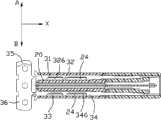
请参阅图2及图3所示,所述绝缘本体20包括安装于电路板(未图示)上的第一绝缘本体21及堆叠于第一绝缘本体21上的第二绝缘本体22。所述第一、第二绝缘本体21、22均具有收容端子30并交替设置的第一端子槽23及第二端子槽24,以及设置于第一、第二绝缘本体21、22底部的第一、第二凸块211、221,其中第一、第二端子槽23、24在第一、第二绝缘本体21、22中排列成并列的两排。第一绝缘本体21顶部还设有与第二凸块221配合的凹槽212以将第一、第二绝缘本体21、22相固持。所述第一凸块211用以安装于电路板上以定位电连接器100。所述第一、第二绝缘本体21、22还设有位于两排端子槽中间用以收容所述金属板40的收容槽25。Please refer to FIG. 2 and FIG. 3 , the
请参阅图2及图4所示,所述端子30分为两排设置于所述绝缘本体20内。其中第一排中交替设置第一端子31及第二端子32,第二排中交替设置第三端子33及第四端子34。在制造端子30时,所述第一端子31与其并列的第三端子33是连接于同一条第一料带35上;第二端子32与其并列的第四端子34是连接于同一条第二料带36上。其中,第一端子31与第四端子34的结构相同,第二端子32与第三端子33的结构相同。第一、第二、第三、第四端子31、32、33、34分别具有第一、第二、第三、第四主体部311、321、331、341,自第一、第二、第三、第四主体部311、321、331、341延伸的第一、第二、第三、第四接触部312、322、332、342及延伸出绝缘本体20的第一、第二、第三、第四焊接部313、323、333、343。在电连接器100中,所述第一、第二、第三、第四主体部311、321、331、341均具有相同的外朝第一方向A的第一侧缘3111、3211、3311、3411及相同的外朝与第一方向A相反的第二方向B的第二侧缘3112、3212、3312、3412。所述第一、第二、第三、第四主体部311、321、331、341分别具有第一、第二、第三、第四实体部314、324、334、344及第一、第二、第三、第四开口部315、325、335、345。在本实施方式中,所述实体部是相对于具有开口的开口部定义,即实体部为连续的金属实体构成。其中第一、第三实体部314、334分别位于第一、第三主体部311、331的第二侧缘3112、3312;第一、第三开口部315、335分别位于第一、第三主体部311、331的第一侧缘3111、3311;第二、第四实体部324、344分别位于第二、第四主体部321、341的第一侧缘3211、3411;第二、第四开口部325、345分别位于第二、第四主体部321、341的第二侧缘3212、3412。第一、第二、第三、第四开口部315、325、335、345上分别具有贯穿第一、第二、第三、第四主体部311、321、331、341的第一、第二、第三、第四开口316、326、336、346。其中,所述第一端子31上的第一开口316背离所述第一实体部314向第一方向A延伸,即使所述第一开口316是相对整个第一主体部311偏向第一方向A;所述第二端子32上的第二开口326背离所述第二实体部324向与第一方向相反的第二方向B延伸,即使所述第二开口326是相对整个第二主体部321偏向第二方向B,以此使第一开口316及第二开口326错开设置。从而,在电连接器100中,由于第一端子31及第二端子32设置在同一排,相邻的第一端子31的第一开口316正对所述第二端子32的第二实体部324,而第二端子32的第二开口326正对所述第一端子31的第一实体部314,这样使第一端子31及第二端子32的金属部分正对的重合部分面积相对减少,从而减少相邻第一、第二端子31、32之间所能够产生电容效应的正对面积而减少电容(电容与正对面积成正比),从而增大端子间的特征阻抗以满足高频信号传输的需要,使高频信号可以稳定传输。同时,正对面积的减少也可以减少在信号传输过程中相邻端子所传输信号的串扰。Please refer to FIG. 2 and FIG. 4 , the
请再参阅图4所示,第三端子33及第四端子34交替排列于另一排,同第一端子31一样,第三端子33的第三开口336背离所述第三实体部334向第一方向A延伸,使所述第三开口336相对整个第三主体部331偏向第一方向A;而同第二端子32一样,第四端子34的第四开口346背离所述第四实体部344向第二方向B延伸,使所述第四开口346相对整个第四主体部341偏向第二方向B,从而如同第一端子31及第二端子32的设置,相邻的第三端子33与第四端子34的金属部分正对的重合部分面积相对减少,同样可减少信号传输过程中相邻第三、第四端子33、34所传输信号的串扰。Please refer to FIG. 4 again, the
请再参阅图4所示,所述第一端子31及第三端子33是连接于第一料带35上,而第二端子32及第四端子34是连接于第二料带36上,同时由于第一端子31与第四端子34的结构相同,第二端子32与第三端子33的结构相同,故设并列的第一端子31及第三端子33组成第一端子组37,并列的第二端子32及第四端子34组成第二端子组38,则第一端子组37的整体结构与第二端子组38相同,而在电连接器100中,第二端子组38可以看做为将第一端子组37转动180度而成,从而使所述第一、第三端子31、34的第一、第三开口316、336与第二、第四端子32、34的第二、第四开口326、346的偏离方向相反。这样一来,只需设计一组端子组即可实现上述结构,从而减少端子模具设计及制造的时间,降低制造成本。Please refer to Fig. 4 again, the
请参阅图2所示,所述金属板40设置在两排端子30之间,以将两排端子30分隔开从而避免两排端子30中并列的端子30之间的信号串扰。Please refer to FIG. 2 , the
请参阅图2、图5及图6所示,该电连接器100组装时,采用如下组装步骤:提供绝缘本体20;将并列的第一端子31及第三端子33沿X方向同时组装入所述第一端子槽23内,并使第一、第三开口316、336偏向第一方向A;将并列的第二端子32及第四端子34同样沿X方向组装入第二端子槽24内,并使第二、第四开口326、346偏向第二方向B;其中,X方向同时垂直于第一方向A及第二方向B;将金属板40组装入绝缘本体20的收容槽25中。该组装步骤将第一端子组37(第一、第三端子31、33)及第二端子组38(第二、第四端子32、34)先后组装,组装方便,利用现有设备即可完成,降低了电连接器100的生产成本。Please refer to Fig. 2, Fig. 5 and Fig. 6, when the
当然,除上述实施方式外,本发明电连接器100中的端子30还可采用其他实施方式。Of course, in addition to the above-mentioned embodiments, the terminal 30 in the
如:请参阅图7所示,为端子的第二种实施方式,在第一种实施方式中,由于第一端子31的第一焊接部313相对于第一主体部311偏离于一侧,故将第一端子31翻转180度形成第四端子34时,只能够将第四端子34安装于相对的第二排中,这样,当仅需要一排端子,而焊接部需要焊接于在同一排时,该第一端子31的结构不能满足要求。在第二种实施方式中,端子30′焊接于电路板上的焊接部33′为对称结构,故当相邻端子30′的开口向相反方向偏离而使得两相邻端子30′为同一结构端子30′翻转180度而形成时,端子30′对称的焊接部33′翻转180度前后并无改变,可焊接于同一排,同时,若将此端子30′结构用于第一种实施方式中,第一、第二、第三、第四端子31、32、33、34均可以采用此种结构,从而进一步降低了端子的设计及制造成本。For example: Please refer to FIG. 7, which is the second embodiment of the terminal. In the first embodiment, since the
又如:请参阅图8所示,为端子的第三种实施方式,在第一种实施方式中,端子30的开口呈向一侧开放式,在本实施方式中,端子30″的开口313″为封闭式,端子30″的主体部31″同样具有实体部311″及开口部312″,开口部312″上的开口313″自四周均有金属以提高端子30″的整体强度。如同第一种实施方式中的端子30一样,本实施方式中的开口313″相对整个主体部31″偏向于第一方向A或第二方向B,从而可达到与第一种实施方式中端子30相同的效果。当然,第二种实施方式中端子30′的开口也可采用本实施方式中开口313″的封闭式样态,在此不再赘述。Another example: Please refer to FIG. 8, which is the third embodiment of the terminal. In the first embodiment, the opening of the terminal 30 is open to one side. In this embodiment, the
除上述实施方式外,本发明电连接器100中的绝缘本体20还可采用其他实施方式。In addition to the above-mentioned embodiments, the insulating
如:在所述电连接器100中,可使第一绝缘本体21与第二绝缘本体22的设计为相同结构,从而第一、第二绝缘本体21、22可采用相同的模具及方法制造以降低成本。当电连接器100需要高度较高时,可将第一、第二绝缘本体21、22堆叠使用;而电连接器100需要低构型设计时,可只使用第一、第二绝缘本体21、22其中之一。For example: in the
Claims (5)
Priority Applications (2)
| Application Number | Priority Date | Filing Date | Title |
|---|---|---|---|
| CN2009103084690ACN102044801B (en) | 2009-10-19 | 2009-10-19 | Electric connector and assembling method |
| US12/713,185US7967636B2 (en) | 2009-10-19 | 2010-02-26 | Electrical connector with terminals staggered from each other |
Applications Claiming Priority (1)
| Application Number | Priority Date | Filing Date | Title |
|---|---|---|---|
| CN2009103084690ACN102044801B (en) | 2009-10-19 | 2009-10-19 | Electric connector and assembling method |
Publications (2)
| Publication Number | Publication Date |
|---|---|
| CN102044801A CN102044801A (en) | 2011-05-04 |
| CN102044801Btrue CN102044801B (en) | 2013-05-08 |
Family
ID=43879638
Family Applications (1)
| Application Number | Title | Priority Date | Filing Date |
|---|---|---|---|
| CN2009103084690AExpired - Fee RelatedCN102044801B (en) | 2009-10-19 | 2009-10-19 | Electric connector and assembling method |
Country Status (2)
| Country | Link |
|---|---|
| US (1) | US7967636B2 (en) |
| CN (1) | CN102044801B (en) |
Families Citing this family (5)
| Publication number | Priority date | Publication date | Assignee | Title |
|---|---|---|---|---|
| DE102012005812A1 (en)* | 2012-03-22 | 2013-09-26 | Tyco Electronics Amp Gmbh | Electrical connector with integrated impedance matching element |
| CN102818909A (en)* | 2012-08-27 | 2012-12-12 | 哈姆林电子(苏州)有限公司 | Terminal stamping structure |
| CN108258484B (en)* | 2016-12-28 | 2020-02-21 | 富士康(昆山)电脑接插件有限公司 | Electric connector and combination thereof |
| TWI823997B (en)* | 2018-08-28 | 2023-12-01 | 英屬開曼群島商鴻騰精密科技股份有限公司 | Card edge connector |
| EP3787129B1 (en)* | 2019-08-27 | 2025-07-02 | TE Connectivity Germany GmbH | Contact terminal with at least one impedance control feature |
Citations (4)
| Publication number | Priority date | Publication date | Assignee | Title |
|---|---|---|---|---|
| US7090540B2 (en)* | 2004-04-09 | 2006-08-15 | Japan Aviation Electronics Industry, Limited | Connector in which terminal portions can easily be arranged at a large pitch |
| CN101174742A (en)* | 2006-10-31 | 2008-05-07 | 富士康(昆山)电脑接插件有限公司 | electrical connector |
| CN101394033A (en)* | 2008-10-16 | 2009-03-25 | 达昌电子科技(苏州)有限公司 | Electronic connector |
| CN201608369U (en)* | 2009-10-12 | 2010-10-13 | 富士康(昆山)电脑接插件有限公司 | electrical connector |
Family Cites Families (11)
| Publication number | Priority date | Publication date | Assignee | Title |
|---|---|---|---|---|
| JP3685908B2 (en)* | 1997-05-30 | 2005-08-24 | 富士通コンポーネント株式会社 | High-speed transmission connector |
| US6461202B2 (en)* | 2001-01-30 | 2002-10-08 | Tyco Electronics Corporation | Terminal module having open side for enhanced electrical performance |
| US6612857B2 (en)* | 2001-07-05 | 2003-09-02 | Bernard R. Tolmie | Electrical connector system and method having optical and/or cooling capability |
| US6808420B2 (en)* | 2002-05-22 | 2004-10-26 | Tyco Electronics Corporation | High speed electrical connector |
| JP3746250B2 (en)* | 2002-06-28 | 2006-02-15 | 日本航空電子工業株式会社 | Cable connector |
| US7270573B2 (en)* | 2002-08-30 | 2007-09-18 | Fci Americas Technology, Inc. | Electrical connector with load bearing features |
| JP4212956B2 (en)* | 2003-05-27 | 2009-01-21 | 富士通コンポーネント株式会社 | Balanced transmission connector |
| US7059914B2 (en)* | 2004-02-20 | 2006-06-13 | Advanced Connectek, Inc. | HDMI plug connector |
| JP4663741B2 (en)* | 2005-02-22 | 2011-04-06 | モレックス インコーポレイテド | Differential signal connector having wafer type structure |
| TWM331787U (en)* | 2007-11-09 | 2008-05-01 | Advanced Connectek Inc | Micro connector |
| US7682192B2 (en)* | 2007-12-05 | 2010-03-23 | Ohio Associated Enterprises, Llc | Electrical receptacle and circuit board with controlled skew |
- 2009
- 2009-10-19CNCN2009103084690Apatent/CN102044801B/ennot_activeExpired - Fee Related
- 2010
- 2010-02-26USUS12/713,185patent/US7967636B2/ennot_activeExpired - Fee Related
Patent Citations (5)
| Publication number | Priority date | Publication date | Assignee | Title |
|---|---|---|---|---|
| US7090540B2 (en)* | 2004-04-09 | 2006-08-15 | Japan Aviation Electronics Industry, Limited | Connector in which terminal portions can easily be arranged at a large pitch |
| CN100421307C (en)* | 2004-04-09 | 2008-09-24 | 日本航空电子工业株式会社 | Connectors that can easily set terminal sections at large pitches |
| CN101174742A (en)* | 2006-10-31 | 2008-05-07 | 富士康(昆山)电脑接插件有限公司 | electrical connector |
| CN101394033A (en)* | 2008-10-16 | 2009-03-25 | 达昌电子科技(苏州)有限公司 | Electronic connector |
| CN201608369U (en)* | 2009-10-12 | 2010-10-13 | 富士康(昆山)电脑接插件有限公司 | electrical connector |
Also Published As
| Publication number | Publication date |
|---|---|
| CN102044801A (en) | 2011-05-04 |
| US7967636B2 (en) | 2011-06-28 |
| US20110092096A1 (en) | 2011-04-21 |
Similar Documents
| Publication | Publication Date | Title |
|---|---|---|
| TWI549385B (en) | Circuit board for an electrical connector | |
| CN102480070B (en) | Wire and cable connector and manufacture method thereof and method for transmitting signals | |
| TWI703779B (en) | Electrical connector structure | |
| US20200185862A1 (en) | Overmolded lead frame providing contact support and impedance matching properties | |
| JP5756110B2 (en) | Plug-in connection including shielding | |
| TWI593175B (en) | An electrical connector | |
| CN201797103U (en) | electrical connector | |
| CN102694308B (en) | electrical connector | |
| CN201608369U (en) | electrical connector | |
| US9444160B2 (en) | Electrical connector | |
| TWM500382U (en) | Electrical connector and combination thereof | |
| CN205335540U (en) | electrical connector | |
| CN102044801B (en) | Electric connector and assembling method | |
| JP4722712B2 (en) | Portable radio terminal or small electronic device using multipolar connector and multipolar connector | |
| JP2005503656A (en) | Impedance adjusted connector | |
| KR20150031199A (en) | Electrical Connector | |
| TWI515983B (en) | Method of manufacturing a connector having a narrow-pitch contact group and connector | |
| US20120138443A1 (en) | Switch with sinuated air-passageway | |
| US20140193992A1 (en) | Electrical connector having improved shileding plate | |
| CN101710660B (en) | Electrical connector with matching coupling | |
| TWI416821B (en) | Electrical connector and method of assembling the same | |
| CN205122833U (en) | Electronic connector | |
| US7922500B2 (en) | Electrical connector | |
| CN209045870U (en) | Electrical connector and its circuit board | |
| US20080293309A1 (en) | Connector with improved contact for transmitting high current |
Legal Events
| Date | Code | Title | Description |
|---|---|---|---|
| C06 | Publication | ||
| PB01 | Publication | ||
| C10 | Entry into substantive examination | ||
| SE01 | Entry into force of request for substantive examination | ||
| C14 | Grant of patent or utility model | ||
| GR01 | Patent grant | ||
| C17 | Cessation of patent right | ||
| CF01 | Termination of patent right due to non-payment of annual fee | Granted publication date:20130508 Termination date:20131019 |