CN102044579B - Solar cell - Google Patents
Solar cellDownload PDFInfo
- Publication number
- CN102044579B CN102044579BCN2010105350624ACN201010535062ACN102044579BCN 102044579 BCN102044579 BCN 102044579BCN 2010105350624 ACN2010105350624 ACN 2010105350624ACN 201010535062 ACN201010535062 ACN 201010535062ACN 102044579 BCN102044579 BCN 102044579B
- Authority
- CN
- China
- Prior art keywords
- region
- solar cell
- substrate
- emitter
- insulating
- Prior art date
- Legal status (The legal status is an assumption and is not a legal conclusion. Google has not performed a legal analysis and makes no representation as to the accuracy of the status listed.)
- Active
Links
- 239000000758substrateSubstances0.000claimsabstractdescription162
- 238000002161passivationMethods0.000claimsdescription177
- 239000004065semiconductorSubstances0.000claimsdescription21
- 239000004020conductorSubstances0.000claimsdescription8
- 239000010410layerSubstances0.000description287
- 238000000034methodMethods0.000description38
- 238000004519manufacturing processMethods0.000description33
- 230000015572biosynthetic processEffects0.000description26
- 239000000463materialSubstances0.000description25
- 229910021417amorphous siliconInorganic materials0.000description18
- 239000000969carrierSubstances0.000description18
- 229910052814silicon oxideInorganic materials0.000description18
- 230000008569processEffects0.000description17
- 239000012535impuritySubstances0.000description16
- VYPSYNLAJGMNEJ-UHFFFAOYSA-NSilicium dioxideChemical compoundO=[Si]=OVYPSYNLAJGMNEJ-UHFFFAOYSA-N0.000description14
- 230000000694effectsEffects0.000description13
- 238000000623plasma-assisted chemical vapour depositionMethods0.000description10
- 230000006798recombinationEffects0.000description8
- 238000005215recombinationMethods0.000description8
- 230000008034disappearanceEffects0.000description7
- 230000001070adhesive effectEffects0.000description5
- 238000005530etchingMethods0.000description5
- XUIMIQQOPSSXEZ-UHFFFAOYSA-NSiliconChemical compound[Si]XUIMIQQOPSSXEZ-UHFFFAOYSA-N0.000description4
- 239000000853adhesiveSubstances0.000description4
- QVGXLLKOCUKJST-UHFFFAOYSA-Natomic oxygenChemical compound[O]QVGXLLKOCUKJST-UHFFFAOYSA-N0.000description4
- 229910052760oxygenInorganic materials0.000description4
- 239000001301oxygenSubstances0.000description4
- 229910052710siliconInorganic materials0.000description4
- 239000010703siliconSubstances0.000description4
- GYHNNYVSQQEPJS-UHFFFAOYSA-NGalliumChemical compound[Ga]GYHNNYVSQQEPJS-UHFFFAOYSA-N0.000description3
- PXHVJJICTQNCMI-UHFFFAOYSA-NNickelChemical compound[Ni]PXHVJJICTQNCMI-UHFFFAOYSA-N0.000description3
- 229910052782aluminiumInorganic materials0.000description3
- XAGFODPZIPBFFR-UHFFFAOYSA-NaluminiumChemical compound[Al]XAGFODPZIPBFFR-UHFFFAOYSA-N0.000description3
- 238000000151depositionMethods0.000description3
- 239000002003electrode pasteSubstances0.000description3
- 229910052733galliumInorganic materials0.000description3
- 229910021478group 5 elementInorganic materials0.000description3
- 229910052738indiumInorganic materials0.000description3
- APFVFJFRJDLVQX-UHFFFAOYSA-Nindium atomChemical compound[In]APFVFJFRJDLVQX-UHFFFAOYSA-N0.000description3
- 238000009413insulationMethods0.000description3
- 238000012986modificationMethods0.000description3
- 230000004048modificationEffects0.000description3
- 229910021420polycrystalline siliconInorganic materials0.000description3
- -1regionSubstances0.000description3
- ZOXJGFHDIHLPTG-UHFFFAOYSA-NBoronChemical compound[B]ZOXJGFHDIHLPTG-UHFFFAOYSA-N0.000description2
- OAICVXFJPJFONN-UHFFFAOYSA-NPhosphorusChemical compound[P]OAICVXFJPJFONN-UHFFFAOYSA-N0.000description2
- 229910052581Si3N4Inorganic materials0.000description2
- 229910052787antimonyInorganic materials0.000description2
- WATWJIUSRGPENY-UHFFFAOYSA-Nantimony atomChemical compound[Sb]WATWJIUSRGPENY-UHFFFAOYSA-N0.000description2
- 229910052785arsenicInorganic materials0.000description2
- RQNWIZPPADIBDY-UHFFFAOYSA-Narsenic atomChemical compound[As]RQNWIZPPADIBDY-UHFFFAOYSA-N0.000description2
- 229910052796boronInorganic materials0.000description2
- 239000010949copperSubstances0.000description2
- 229910021419crystalline siliconInorganic materials0.000description2
- 238000002425crystallisationMethods0.000description2
- 230000008025crystallizationEffects0.000description2
- 230000008021depositionEffects0.000description2
- 238000010292electrical insulationMethods0.000description2
- 239000010931goldSubstances0.000description2
- 239000007769metal materialSubstances0.000description2
- 238000007254oxidation reactionMethods0.000description2
- 229910052698phosphorusInorganic materials0.000description2
- 239000011574phosphorusSubstances0.000description2
- XHXFXVLFKHQFAL-UHFFFAOYSA-Nphosphoryl trichlorideChemical compoundClP(Cl)(Cl)=OXHXFXVLFKHQFAL-UHFFFAOYSA-N0.000description2
- 238000000206photolithographyMethods0.000description2
- 229920005591polysiliconPolymers0.000description2
- 238000005036potential barrierMethods0.000description2
- HQVNEWCFYHHQES-UHFFFAOYSA-Nsilicon nitrideChemical compoundN12[Si]34N5[Si]62N3[Si]51N64HQVNEWCFYHHQES-UHFFFAOYSA-N0.000description2
- 239000010936titaniumSubstances0.000description2
- 238000001039wet etchingMethods0.000description2
- RYGMFSIKBFXOCR-UHFFFAOYSA-NCopperChemical compound[Cu]RYGMFSIKBFXOCR-UHFFFAOYSA-N0.000description1
- XEEYBQQBJWHFJM-UHFFFAOYSA-NIronChemical compound[Fe]XEEYBQQBJWHFJM-UHFFFAOYSA-N0.000description1
- 229910019213POCl3Inorganic materials0.000description1
- BQCADISMDOOEFD-UHFFFAOYSA-NSilverChemical compound[Ag]BQCADISMDOOEFD-UHFFFAOYSA-N0.000description1
- 229910006404SnO 2Inorganic materials0.000description1
- ATJFFYVFTNAWJD-UHFFFAOYSA-NTinChemical compound[Sn]ATJFFYVFTNAWJD-UHFFFAOYSA-N0.000description1
- RTAQQCXQSZGOHL-UHFFFAOYSA-NTitaniumChemical compound[Ti]RTAQQCXQSZGOHL-UHFFFAOYSA-N0.000description1
- 230000008901benefitEffects0.000description1
- 230000005540biological transmissionEffects0.000description1
- 239000003245coalSubstances0.000description1
- 229910052802copperInorganic materials0.000description1
- 230000007547defectEffects0.000description1
- 229910052732germaniumInorganic materials0.000description1
- GNPVGFCGXDBREM-UHFFFAOYSA-Ngermanium atomChemical compound[Ge]GNPVGFCGXDBREM-UHFFFAOYSA-N0.000description1
- PCHJSUWPFVWCPO-UHFFFAOYSA-NgoldChemical compound[Au]PCHJSUWPFVWCPO-UHFFFAOYSA-N0.000description1
- 229910052737goldInorganic materials0.000description1
- 230000031700light absorptionEffects0.000description1
- 229910021421monocrystalline siliconInorganic materials0.000description1
- 229910052759nickelInorganic materials0.000description1
- 239000012811non-conductive materialSubstances0.000description1
- 239000003921oilSubstances0.000description1
- 230000002093peripheral effectEffects0.000description1
- 230000009467reductionEffects0.000description1
- 230000008521reorganizationEffects0.000description1
- 238000007650screen-printingMethods0.000description1
- 229910052709silverInorganic materials0.000description1
- 239000004332silverSubstances0.000description1
- 239000002356single layerSubstances0.000description1
- 238000004544sputter depositionMethods0.000description1
- JBQYATWDVHIOAR-UHFFFAOYSA-NtellanylidenegermaniumChemical compound[Te]=[Ge]JBQYATWDVHIOAR-UHFFFAOYSA-N0.000description1
- 229910052719titaniumInorganic materials0.000description1
Images


Classifications
- H—ELECTRICITY
- H10—SEMICONDUCTOR DEVICES; ELECTRIC SOLID-STATE DEVICES NOT OTHERWISE PROVIDED FOR
- H10F—INORGANIC SEMICONDUCTOR DEVICES SENSITIVE TO INFRARED RADIATION, LIGHT, ELECTROMAGNETIC RADIATION OF SHORTER WAVELENGTH OR CORPUSCULAR RADIATION
- H10F77/00—Constructional details of devices covered by this subclass
- H10F77/30—Coatings
- H10F77/306—Coatings for devices having potential barriers
- H10F77/311—Coatings for devices having potential barriers for photovoltaic cells
- H—ELECTRICITY
- H10—SEMICONDUCTOR DEVICES; ELECTRIC SOLID-STATE DEVICES NOT OTHERWISE PROVIDED FOR
- H10F—INORGANIC SEMICONDUCTOR DEVICES SENSITIVE TO INFRARED RADIATION, LIGHT, ELECTROMAGNETIC RADIATION OF SHORTER WAVELENGTH OR CORPUSCULAR RADIATION
- H10F10/00—Individual photovoltaic cells, e.g. solar cells
- H10F10/10—Individual photovoltaic cells, e.g. solar cells having potential barriers
- H10F10/16—Photovoltaic cells having only PN heterojunction potential barriers
- H10F10/164—Photovoltaic cells having only PN heterojunction potential barriers comprising heterojunctions with Group IV materials, e.g. ITO/Si or GaAs/SiGe photovoltaic cells
- H10F10/165—Photovoltaic cells having only PN heterojunction potential barriers comprising heterojunctions with Group IV materials, e.g. ITO/Si or GaAs/SiGe photovoltaic cells the heterojunctions being Group IV-IV heterojunctions, e.g. Si/Ge, SiGe/Si or Si/SiC photovoltaic cells
- H10F10/166—Photovoltaic cells having only PN heterojunction potential barriers comprising heterojunctions with Group IV materials, e.g. ITO/Si or GaAs/SiGe photovoltaic cells the heterojunctions being Group IV-IV heterojunctions, e.g. Si/Ge, SiGe/Si or Si/SiC photovoltaic cells the Group IV-IV heterojunctions being heterojunctions of crystalline and amorphous materials, e.g. silicon heterojunction [SHJ] photovoltaic cells
- H—ELECTRICITY
- H10—SEMICONDUCTOR DEVICES; ELECTRIC SOLID-STATE DEVICES NOT OTHERWISE PROVIDED FOR
- H10F—INORGANIC SEMICONDUCTOR DEVICES SENSITIVE TO INFRARED RADIATION, LIGHT, ELECTROMAGNETIC RADIATION OF SHORTER WAVELENGTH OR CORPUSCULAR RADIATION
- H10F77/00—Constructional details of devices covered by this subclass
- H10F77/20—Electrodes
- H10F77/206—Electrodes for devices having potential barriers
- H10F77/211—Electrodes for devices having potential barriers for photovoltaic cells
- H10F77/219—Arrangements for electrodes of back-contact photovoltaic cells
- Y—GENERAL TAGGING OF NEW TECHNOLOGICAL DEVELOPMENTS; GENERAL TAGGING OF CROSS-SECTIONAL TECHNOLOGIES SPANNING OVER SEVERAL SECTIONS OF THE IPC; TECHNICAL SUBJECTS COVERED BY FORMER USPC CROSS-REFERENCE ART COLLECTIONS [XRACs] AND DIGESTS
- Y02—TECHNOLOGIES OR APPLICATIONS FOR MITIGATION OR ADAPTATION AGAINST CLIMATE CHANGE
- Y02E—REDUCTION OF GREENHOUSE GAS [GHG] EMISSIONS, RELATED TO ENERGY GENERATION, TRANSMISSION OR DISTRIBUTION
- Y02E10/00—Energy generation through renewable energy sources
- Y02E10/50—Photovoltaic [PV] energy
- Y02E10/547—Monocrystalline silicon PV cells
Landscapes
- Photovoltaic Devices (AREA)
- Life Sciences & Earth Sciences (AREA)
- Engineering & Computer Science (AREA)
- Sustainable Energy (AREA)
- Sustainable Development (AREA)
Abstract
Translated fromChinese
Description
Translated fromChinese技术领域technical field
本发明的实施方式涉及太阳能电池。 Embodiments of the present invention relate to solar cells. the
背景技术Background technique
近来,由于认为现有能源(如石油和煤)是会被耗尽的,因此对于代替现有能源的另选能源越来越感兴趣。在这些另选能源中,从太阳能产生电能的太阳能电池尤其受到关注。 Recently, since existing energy sources such as oil and coal are believed to be exhausted, there has been increasing interest in alternative energy sources to replace existing energy sources. Among these alternative energy sources, solar cells, which generate electrical energy from solar energy, are of particular interest. the
太阳能电池通常包括具有不同导电类型(例如p型和n型)并且形成p-n结的半导体部分、和分别连接到不同导电类型的半导体部分的电极。 A solar cell generally includes semiconductor portions having different conductivity types (eg, p-type and n-type) and forming a p-n junction, and electrodes respectively connected to the semiconductor portions of different conductivity types. the
当光入射到太阳能电池上时,在半导体部分中产生多个电子-空穴对。通过光电效应,电子-空穴对分离成电子和空穴。因此,分离的电子移动到n型半导体,分离的空穴移动到p型半导体,随后分别通过电连接到n型半导体和p型半导体的电极来收集这些电子和空穴。这些电极使用电线而彼此连接并因此获得电能。 When light is incident on the solar cell, a plurality of electron-hole pairs are generated in the semiconductor portion. By the photoelectric effect, electron-hole pairs are separated into electrons and holes. Accordingly, separated electrons move to the n-type semiconductor, and separated holes move to the p-type semiconductor, which are then collected by electrodes electrically connected to the n-type semiconductor and the p-type semiconductor, respectively. These electrodes are connected to each other using electric wires and thus obtain electric power. the
发明内容Contents of the invention
在一方面,存在一种太阳能电池,该太阳能电池包括:第一导电类型的基板;位于所述基板上的与所述第一导电类型相反的第二导电类型的射极区;位于所述基板上并与所述射极区分隔开的所述第一导电类型的第一场区(field region);电连接到所述射极区的第一电极;电连接到所述第一场区的第二电极;以及位于所述射极区和所述第一场区中的至少一个上的绝缘区。 In one aspect, there is a solar cell comprising: a substrate of a first conductivity type; an emitter region of a second conductivity type opposite to the first conductivity type on the substrate; A first field region (field region) of the first conductivity type on and separated from the emitter region; a first electrode electrically connected to the emitter region; a first electrode electrically connected to the first field region a second electrode; and an insulating region on at least one of the emitter region and the first field region. the
当所述绝缘区位于所述第一场区上时,所述绝缘区可以位于所述第一场区的边缘上。 When the insulating region is located on the first field region, the insulating region may be located on an edge of the first field region. the
当所述绝缘区位于所述第一场区上时,所述绝缘区可以具有暴露出所述第一场区的一部分的至少一个开口。 When the insulating region is located on the first field region, the insulating region may have at least one opening exposing a portion of the first field region. the
所述绝缘区可以位于所述射极区和所述第一场区之间。 The insulating region may be located between the emitter region and the first field region. the
所述绝缘区可以包括直接接触所述基板的一部分。 The insulating region may include a portion directly contacting the substrate. the
所述绝缘区可以直接接触在所述射极区和所述第一场区之间暴露出的所述基板。 The insulating region may directly contact the substrate exposed between the emitter region and the first field region. the
所述射极区可以包括位于第一高度的第一部分、和位于高于所述第一高度的第二高度的第二部分。 The emitter region may include a first portion at a first height, and a second portion at a second height higher than the first height. the
当所述绝缘区位于所述射极区上时,所述绝缘区可以位于所述射极区的所述第一部分上。 When the insulating region is on the emitter region, the insulating region may be on the first portion of the emitter region. the
所述绝缘区可以具有暴露所述射极区的所述第一部分的一部分的至少一个开口。 The insulating region may have at least one opening exposing a portion of the first portion of the emitter region. the
所述太阳能电池还可以包括位于所述基板和所述第一场区之间以及所述基板和所述射极区之间的钝化层。 The solar cell may further include a passivation layer between the substrate and the first field region and between the substrate and the emitter region. the
所述钝化层可以包括位于所述基板和所述第一场区之间的第一部分以及位于所述基板和所述射极区之间的第二部分。 The passivation layer may include a first portion between the substrate and the first field region and a second portion between the substrate and the emitter region. the
所述钝化层的所述第二部分可以具有与所述射极区相同的平面形状。 The second portion of the passivation layer may have the same planar shape as the emitter region. the
所述钝化层可以位于所述第一场区和所述射极区之间。 The passivation layer may be located between the first field region and the emitter region. the
所述钝化层可以在所述第一场区和所述射极区之间延伸,并且可以位于所述绝缘区和所述射极区之间。 The passivation layer may extend between the first field region and the emitter region, and may be located between the insulating region and the emitter region. the
所述钝化层可以具有暴露所述射极区的所述第一部分的至少一个开 口。 The passivation layer may have at least one opening exposing the first portion of the emitter region. the
当所述绝缘区位于所述射极区和所述第一场区上时,所述绝缘区可以位于所述射极区的边缘和所述第一场区的边缘。 When the insulating region is located on the emitter region and the first field region, the insulating region may be located at an edge of the emitter region and an edge of the first field region. the
所述太阳能电池还可以包括位于所述射极区和所述第一电极之间的第一辅助电极、以及位于所述第一场区和所述第二电极之间的第二辅助电极。 The solar cell may further include a first auxiliary electrode located between the emitter region and the first electrode, and a second auxiliary electrode located between the first field region and the second electrode. the
所述第一辅助电极和所述第二辅助电极可以由透明导电材料形成。 The first auxiliary electrode and the second auxiliary electrode may be formed of a transparent conductive material. the
所述射极区和所述第一场区可以位于所述基板的没有光入射的表面上。 The emitter region and the first field region may be located on a surface of the substrate on which no light is incident. the
所述基板可以由晶体半导体形成,并且所述射极区和所述第一场区可以由非晶半导体形成。 The substrate may be formed of a crystalline semiconductor, and the emitter region and the first field region may be formed of an amorphous semiconductor. the
所述太阳能电池还可以包括与所述第一场区相对地位于所述基板上的第二场区。 The solar cell may further include a second field on the substrate opposite to the first field. the
所述太阳能电池还可以包括位于所述基板和所述第二场区之间的钝化层。 The solar cell may further include a passivation layer between the substrate and the second field region. the
附图说明Description of drawings
附图被包括进来以提供对本发明的进一步理解,其被并入且构成本说明书的一部分,附图示出了本发明的实施方式,并与说明书一起用于解释本发明的原理。在附图中: The accompanying drawings, which are included to provide a further understanding of the invention and are incorporated in and constitute a part of this specification, illustrate embodiments of the invention and together with the description serve to explain the principle of the invention. In the attached picture:
图1是根据本发明一个实施方式的太阳能电池的部分透视图; Figure 1 is a partial perspective view of a solar cell according to one embodiment of the present invention;
图2是沿图1的线II-II截取的剖面图; Fig. 2 is a sectional view taken along line II-II of Fig. 1;
图3A到3T顺序地示出了图1中所示的太阳能电池的制造方法的每个阶段; 3A to 3T sequentially illustrate each stage of the manufacturing method of the solar cell shown in FIG. 1;
图4A和4B示出了图1中所示的太阳能电池的制造方法中的用于制造多个第一辅助电极和第二辅助电极以及多个第一电极和第二电极的另一种方法; 4A and 4B illustrate another method for manufacturing a plurality of first auxiliary electrodes and second auxiliary electrodes and a plurality of first electrodes and second electrodes in the method of manufacturing a solar cell shown in FIG. 1;
图5是根据本发明另一个实施方式的太阳能电池的部分剖面图; 5 is a partial cross-sectional view of a solar cell according to another embodiment of the present invention;
图6A和6B示出了图5中所示的太阳能电池的制造方法的一部分; 6A and 6B show a part of the manufacturing method of the solar cell shown in FIG. 5;
图7是根据本发明另一个实施方式的太阳能电池的部分剖面图; Figure 7 is a partial cross-sectional view of a solar cell according to another embodiment of the present invention;
图8A到8C示出了图7中所示的太阳能电池的制造方法的一部分; 8A to 8C show a part of the manufacturing method of the solar cell shown in FIG. 7;
图9A到9D示出了图7中所示的太阳能电池的另一制造方法的一部分; 9A to 9D show a part of another manufacturing method of the solar cell shown in FIG. 7;
图10是根据本发明另一个实施方式的太阳能电池的部分剖面图; Figure 10 is a partial cross-sectional view of a solar cell according to another embodiment of the present invention;
图11A到11H示出了图10中所示的太阳能电池的制造方法的一部分; 11A to 11H show a part of the manufacturing method of the solar cell shown in FIG. 10;
图12是根据本发明另一个实施方式的太阳能电池的部分剖面图; 12 is a partial cross-sectional view of a solar cell according to another embodiment of the present invention;
图13是根据本发明另一个实施方式的太阳能电池的部分剖面图;以及 13 is a partial cross-sectional view of a solar cell according to another embodiment of the present invention; and
图14到图17是根据本发明其它实施方式的各种太阳能电池的部分剖面图。 14 to 17 are partial cross-sectional views of various solar cells according to other embodiments of the present invention. the
具体实施方式Detailed ways
以下将参照附图更全面地描述本发明,在附图中示出了本发明的示例性实施方式。然而,本发明可以以很多不同形式实现并且不应被理解为局限于这里阐述的实施方式。 The present invention will be described more fully hereinafter with reference to the accompanying drawings, in which exemplary embodiments of the invention are shown. However, this invention may be embodied in many different forms and should not be construed as limited to the embodiments set forth herein. the
在附图中,为了清楚起见,放大了层、膜、板、区域等的厚度。在整个说明书中,相同标号表示相同元件。应该理解,当将诸如层、膜、区域或基板的元件称为“位于另一元件上”时,它可以直接位于所述另一元件上,或者也可以存在中间元件。相反,当将一元件称为“直接位于另一元件上”时,不存在中间元件。另外,应该理解,当将诸如层、膜、区域或基板的元件称为“完全”位于另一元件上时,它可以位于所述另一元件的整个表面上,而不可以位于所述另一元件的边缘部分上。 In the drawings, the thickness of layers, films, panels, regions, etc., are exaggerated for clarity. Throughout the specification, the same reference numerals refer to the same elements. It will be understood that when an element such as a layer, film, region, or substrate is referred to as being "on" another element, it can be directly on the other element or intervening elements may also be present. In contrast, when an element is referred to as being "directly on" another element, there are no intervening elements present. In addition, it will be understood that when an element such as a layer, film, region, or substrate is referred to as being "entirely" on another element, it can be on the entire surface of the other element and not be on the other element. on the edge of the component. the
现在将详细描述本发明的实施方式,其示例示出在附图中。 Reference will now be made in detail to embodiments of the invention, examples of which are illustrated in the accompanying drawings. the
下面参照附图1和2详细描述根据本发明一个实施方式的太阳能电池。 A solar cell according to an embodiment of the present invention will be described in detail below with reference to FIGS. 1 and 2 . the
图1是根据本发明一个实施方式的太阳能电池的部分透视图。图2是沿图1的线II-II截取的剖面图。 FIG. 1 is a partial perspective view of a solar cell according to an embodiment of the present invention. FIG. 2 is a sectional view taken along line II-II of FIG. 1 . the
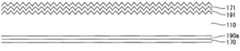
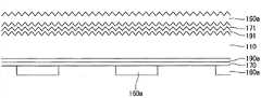
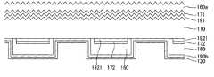
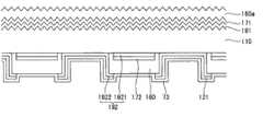
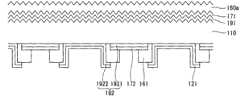
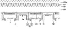
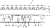
如图1和2所示,根据本发明的一个实施方式的太阳能电池11包括基板110、位于基板110上的光入射表面(在下文中称为″正面″)上的正面钝化层191、位于正面钝化层191上的正面场(FSF)区171、位于FSF区171上的防反射层130、位于基板110的与基板110的正面相对的没有光入射的表面(在下文中称为″背面″)上的背面钝化层192、位于背面钝化层192的一部分上的多个射极区121、位于背面钝化层192的一部分上并与所述多个射极区121隔开的多个背面场(BSF)区172、分别位于所 述多个射极区121上的多个第一辅助电极151、分别位于所述多个BSF区172上的多个第二辅助电极152、分别位于所述多个第一辅助电极151上的多个第一电极141、分别位于多个第二辅助电极152上的多个第二电极142、以及多个绝缘区161,所述多个绝缘区161各自位于彼此相邻的射极区121和BSF区172之间,并且位于BSF区172上。 As shown in FIGS. 1 and 2, a solar cell 11 according to an embodiment of the present invention includes a substrate 110, a front passivation layer 191 on a light incident surface (hereinafter referred to as "front side") on the substrate 110, a front side passivation layer 191 on the front side The front side field (FSF) region 171 on the passivation layer 191, the anti-reflection layer 130 on the FSF region 171, the surface of the substrate 110 opposite to the front side of the substrate 110 without light incidence (hereinafter referred to as "back surface") The backside passivation layer 192 on the backside passivation layer 192, a plurality of emitter regions 121 on a part of the backside passivation layer 192, a plurality of backsides located on a part of the backside passivation layer 192 and separated from the plurality of emitter regions 121 Field (BSF) region 172, a plurality of first auxiliary electrodes 151 respectively located on the plurality of emitter regions 121, a plurality of second auxiliary electrodes 152 respectively located on the plurality of BSF regions 172, respectively located on the plurality of The plurality of first electrodes 141 on the plurality of first auxiliary electrodes 151, the plurality of second electrodes 142 respectively located on the plurality of second auxiliary electrodes 152, and the plurality of insulating regions 161, each of which is located The emitter region 121 and the BSF region 172 adjacent to each other are located between and on the BSF region 172 . the
基板110是由第一导电类型的硅(例如n型硅)形成的半导体基板,但这不是必需的。用于基板110的硅可以是例如单晶硅和多晶硅的晶体硅。当基板110是n型时,基板110可以包含例如磷(P)、砷(As)和锑(Sb)的V族元素的杂质。另选的是,基板110可以是p型的,并且/或者由不同于硅的另一种半导体材料形成。当基板110是p型时,基板110可以包含例如硼(B)、镓(Ga)和铟(In)的III族元素的杂质。 The
可以将基板110的正面粗糙化,以形成相当于不平坦表面的粗糙表面或者具有不平坦特性。 The front surface of the
在基板110正面上的正面钝化层191执行钝化操作,将例如存在于110表面上和基板110表面周围的悬空键的不稳定键转变为稳定键,由此防止或减少由于不稳定键而导致的移动到基板110正面的载流子的重组和/或消失。在本实施方式中,因为正面钝化层191由其中不存在或者几乎不存在杂质的本征非晶硅(a-Si)形成,所以防止或减少了由于杂质而导致的缺陷(例如载流子损失)。另选的是,正面钝化层191可以由氧化硅(SiOx)和/或氮化硅(SiNx)形成。 The
在本实施方式中,正面钝化层191上的FSF区171由非晶硅形成,但是也可以由例如多晶硅的晶体硅形成。FSF区171是杂质区(例如n+型区),相比于基板110来说其掺杂了更多的与基板110相同导电类型的杂质。 In this embodiment, the
因此,通过由于基板110和FSF区171的杂质浓度之间的差异而导致的势垒,防止或减少了空穴向基板110正面的移动。因此,防止或减少了电子和空穴在基板110表面上和在基板110表面的周围的重组和/或消失。按与正面钝化层191相同的方式,FSF区171执行钝化操作,由此防止或减少了载流子的在基板110表面上和基板110表面周围的重组和/或消失。 Accordingly, the movement of holes to the front surface of the
FSF区171上的防反射层130降低入射在太阳能电池11上的光的反射率,并且增大对预定波长带的选择性,由此增加太阳能电池11的效率。防反射层130由SiNx、SiOx、SiNx:H、SiOx:H等形成。在本实施方式中,防反射层130具有单层结构,但是防反射层130也可以具有多层结构,例如在其它实施方式中的双层结构。如果期望,则可以省略防反射层130。按与正面钝化层191相同的方式,防反射层130执行钝化操作。 The
因此,由于通过位于基板110正面上的正面钝化层191、FSF区171和防反射层130的钝化操作而防止或减少了由不稳定键导致的载流子在基板110正面周围的重组和/或消失,所以改善了太阳能电池11的效率。 Therefore, due to the passivation operation by the
在基板110背面上的背面钝化层192包括彼此隔开的多个第一背面钝化层1921(也就是第一部分)和多个第二背面钝化层1922(也就是第二部分)。第一背面钝化层1921和第二背面钝化层1922彼此相邻并且彼此平行地在基板110上沿固定方向延伸。 The
各个第二背面钝化层1922位于绝缘区161的与第二背面钝化层1922相邻的一部分上。因此,各个第一背面钝化层1921不论其形成位置如何都具有相同高度d11,而各个第二背面钝化层1922根据其形成位置具有不同的高度d12和d13。例如,第二背面钝化层1922的中央部分中的高度(也就是位置)d12低于第二背面钝化层1922的两个边缘部分中的高度(也就是位置)d13。在本实施方式中,第一背面钝化层1921的位置d11和第二背面钝化层1922的位置d12彼此相同,但是也可以彼此不同。在本实施方式中,位置(也就是高度)表示基板110的表面与第一钝化层1921和第二钝化层1922各自的上表面之间的最短距离。 Each second
按与正面钝化层191相同的方式,背面钝化层192由非晶硅、氧化硅(SiOx)或氮化硅(SiNx)形成。背面钝化层192执行钝化操作,由此防止或减小由不稳定键导致的移动到基板110背面的载流子的重组和/或消失。 In the same manner as the
第一背面钝化层1921和第二背面钝化层1922各自具有这样的厚度:使得移动到基板110背面的载流子能够穿过第一背面钝化层1921和第二背面钝化层1922中的每一个,并且能够移动到BSF区172和射极区121。例如,背面钝化层192的厚度可以是大约1nm到10nm。 The first
多个BSF区172位于第一背面钝化层1921上,并且与第一背面钝化层1921具有相同的平面形状。因此,BSF区172沿着第一背面钝化层1921以固定方向在第一背面钝化层1921上延伸。按与FSF区171相同的方式,多个BSF区172由非晶硅形成。各个FSF区172是杂质区(例如n+型区),相比于基板110来说其掺杂了更多的与基板110同样导电类型的杂质。按与位于BSF区172下方的第一背面钝化层1921相同的方式,不论其形成位置,各个BSF区172都具有相同的高度d21。在本发明的实施方式中,提到“平面形状”也就表示具有板形状,提到“相同的平面形状”也就表示使得区域和层的平面的延伸方向一致的相同平面形状。 A plurality of
因此,按FSF区171相同的方式,通过由于基板110和BSF区172的杂质浓度之间的差异而导致的势垒,防止或者减少了穿过多个第一背面钝化层1921的载流子(例如空穴)移动到多个第二电极142。因此,防止或减少了电子和空穴在多个第二电极142周围的重组和/或消失。 Therefore, in the same manner as the
多个射极区121位于背面钝化层192的第二背面钝化层1922上,并且与第二背面钝化层1922具有相同的平面形状。因此,射极区121沿着第二背面钝化层1922以固定方向在第二背面钝化层1922上延伸。 The plurality of
如图1和2所示,另选的是,多个射极区121和多个BSF区172位于基板110的背面上。 As shown in FIGS. 1 and 2 , alternatively, the plurality of
各个射极区121是与基板110的导电类型相反的第二导电类型(例如p型)。各个射极区121由不同于基板110的半导体(例如,诸如非晶硅的非晶半导体)形成。因此,除了p-n结之外,多个射极区121和基板110还形成异质结。 Each
按与位于射极区121之下的第二背面钝化层1922相同的方式,各个射极区121根据其形成位置而具有不同的高度。例如,射极区121的中央部分的高度d22小于射极区121的两个边缘部分的高度d23。在本实施方式中,射极区121中央部分的高度d22和BSF区172的高度d21彼此相同,但是也可以彼此不同。在实施方式中,高度表示第一背面钝化层 1921和第二背面钝化层1922各自的表面与BSF区172和射极区121各自的上表面之间的最短距离。高度也可以是基板110的表面与BSF区172和射极区121各自的表面之间的最短距离。 In the same manner as the second
当多个射极区121是p型时,射极区121可以包含例如硼(B)、镓(Ga)和铟(In)的III族元素的杂质。相反,当射极区121是n型时,射极区121可以包含例如磷(P)、砷(As)和锑(Sb)的V族元素的杂质。 When the plurality of
通过由于基板110和射极区121之间的p-n结而产生的内建电势差,将入射在基板110上的光所产生的多个电子一空穴对分解成电子和空穴。随后,分离的电子移动到n型半导体,分离的空穴移动到p型半导体。因此,当基板110是n型并且射极区121是p型时,分离的空穴穿过背面钝化层192的第二背面钝化层1922并移动到射极区121,分离的电子穿过背面钝化层192的第一背面钝化层1921并移动到具有高杂质浓度的BSF区172。 A plurality of electron-hole pairs generated by light incident on the
因为基板110和各个射极区121形成p-n结,所以不同于上述实施方式,当基板110是p型时,射极区121可以是n型。在本例中,分离的电子穿过背面钝化层192的第二背面钝化层1922并移动到射极区121,分离的空穴穿过背面钝化层192的第一背面钝化层1921并移动到BSF区172。 Since the
多个射极区121、多个BSF区172和背面钝化层192执行钝化操作,由此防止或减少由不稳定键导致的载流子在基板110背面上和在基板110背面周围的重组和/或消失。因此,太阳能电池11的效率得到改善。 The plurality of
此外,在本实施方式中,与当射极区121和BSF区172直接位于由晶态半导体材料形成的基板110上时的晶化现象相比,当射极区121和BSF区172位于由本征a-Si形成的背面钝化层192上时的晶化现象得到大大减少。因此,位于非晶硅层(也就是背面钝化层192)上的射极区121和BSF区172的特性得以改善。 Furthermore, in this embodiment mode, compared with the crystallization phenomenon when the
多个绝缘区161由不导电材料形成,例如基于氧化硅的材料,如SiOx、a-SiOx、SiOx:H和a-SiOx:H。 The plurality of insulating
在相邻的第一背面钝化层1921和第二背面钝化层1922之间,并且在第一背面钝化层1921上的BSF区172的边缘部分上,沿着射极区121和BSF区172的延伸方向,各个绝缘区161在基板110上长延伸。因此,各个绝缘区161与BSF区172的一部分交叠。如上所述,各个绝缘区161的一部分与第二背面钝化层1922的一部分和第二背面钝化层1922上的射极区121的一部分交叠。 Between the adjacent first
多个绝缘区161在彼此相邻的射极区121和BSF区172之间的相互绝缘,由此防止射极区121和BSF区172之间的短路,防止载流子的泄露,并且防止由于彼此物理隔开的射极区121和BSF区172之间的电气干扰而导致的载流子损失。因此,减少了太阳能电池11的漏电量。 The plurality of insulating
在本发明的实施方式中,第二背面钝化层1922包括几个部分,一个部分(第一部分)在基板110上平行于基板110延伸,另一部分(第二部分)沿着绝缘区161的侧面延伸,并且又一部分(第三部分)在平行于基板110的绝缘区161的表面上平行延伸。同样,射极区121包括几个部分,一个部分(第一部分)平行于基板110延伸,另一部分(第二部分)平行于绝缘区161的侧面延伸,并且又一部分(第三部分)与平行于基板110的绝缘区161的表面平行地延伸。在其它实施方式中,第二背面钝化层1922的一个或更多个部分不需要与射极区121的一个或更多个部分的平面形状相匹配,反之亦然。 In an embodiment of the present invention, the second
多个射极区121上的多个第一辅助电极151沿着射极区121延伸,并且电连接到射极区121。此外,如图1和2所示,各个第一辅助电极151位于绝缘区161上,与各个射极区121相邻。因此,第一辅助电极151保护第一辅助电极151之下的射极区121免受空气中氧气的影响,由此防止了由于氧化反应导致的射极区121的特性改变。 The plurality of first
如上所述,因为各个射极区121根据其形成位置而具有不同的高度d22和d23,所以各个第一辅助电极151根据其形成位置而具有不同的厚度。例如,位于射极区121的中央部分的第一辅助电极151的厚度大于位于射极区121的两个边缘部分以及位于绝缘区161上的第一辅助电极151的厚度。 As described above, since the
多个BSF区172上的多个第二辅助电极152沿着BSF区172延伸,并且电连接到BSF区172。不同于第一辅助电极151,各个第二辅助电极152具有均匀的厚度,或者实质上均匀的厚度,除了边缘处的小部分之外。 The plurality of second
类似于射极区121,第二辅助电极152和绝缘区161保护BSF区172免受空气中氧气的影响,由此防止了由于氧化反应而导致的BSF区172的特性改变。 Similar to the
多个第一辅助电极151和第二辅助电极152由具有导电性的透明导电材料形成。透明导电材料的示例包括ITO、ZnO、SnO2、TCO等或其组合,或者通过掺杂这些材料或与铝(Al)、锗(Ge)、镓(Ga)、铁(Fe)等的组合而获得的材料。 The plurality of first
多个第一辅助电极151和第二辅助电极152分别传输载流子(例如分别移动到射极区121和BSF区172的空穴和电子),并且反射穿过基板110和背面钝化层192到达基板110的光,由此用作增加在基板110上的入射光量的反射器。 The plurality of first
在射极区121中央部分中存在的载流子的量大于在射极区121两个边缘部分中存在的载流子的量。因此,在实施方式中,因为第一辅助电极151中央部分的厚度大于第一辅助电极151边缘部分的厚度,所以传输到对应于射极区121的第一辅助电极151的载流子量增加。另选的是,可以省略多个第一辅助电极151和第二辅助电极152。 The amount of carriers present in the central portion of
多个第一辅助电极151上的多个第一电极141沿着第一辅助电极151而长延伸,并且电子和物理连接到第一辅助电极151。在图1和2中第一电极141和在第一电极141之下的第一辅助电极151具有相同的平面形状,但是它们可以具有不同的平面形状。 The plurality of
各个第一电极141收集移动到对应的射极区121并且通过第一辅助电极151传输的载流子(例如空穴)。因为第一辅助电极151如上所述根据其形成位置而具有不同的厚度,所以改善了从射极区121到对应的第一辅助电极151的载流子收集效率。因此,增加了输出到第一电极141的载流子量。 Each
多个第二辅助电极152上的多个第二电极142沿着第二辅助电极152 而长延伸,并且电子和物理连接到第二辅助电极152。在图1和2中第二电极142和位于第二电极142之下的第二辅助电极152具有相同的平面形状,但是它们也可以具有不同的平面形状。各个第二电极142收集移动到的对应BSF区172并且通过第二辅助电极152传输的载流子(例如电子)。 The plurality of
多个第一电极141和第二电极142可以由从包括镍(Ni)、铜(Cu)、银(Ag)、铝(Al)、锡(Sn)、锌(Zn)、铟(In)、钛(Ti)、金(Au)和其组合物的组中选择的至少一种导电材料形成。也可以使用其它导电材料。 The plurality of
在本实施方式中,由透明导电材料形成的多个第一辅助电极151和第二辅助电极152位于由例如非晶硅的半导体材料形成的多个射极区121和多个BSF区172与由金属材料形成的多个第一电极141和第二电极142之间,由此改善了具有低粘合强度(粘合特性)的半导体材料和金属材料之间的粘合强度。因此,改善了射极区121和第一电极141之间的粘合强度以及BSF区172和第二电极142之间的粘合强度。 In this embodiment, the plurality of first
此外,在射极区121和第一电极141之间以及在BSF区172和第二电极142之间形成欧姆接触,由此改善射极区121和第一电极141之间的导电性以及BSF区172和第二电极142之间的导电性。因此,增加了第一电极141和第二电极142的载流子传输效率。 In addition, ohmic contacts are formed between the
如果省略多个第一辅助电极151和第二辅助电极152,则各个第一电极141和各个第二电极142分别直接位于对应的射极区121和对应的BSF区172上。 If the plurality of first
具有上述结构的太阳能电池11是这样的太阳能电池:其中多个第一电极141和第二电极142位于基板110的没有光入射的背面上,并且基板110和多个射极区121由不同种类的半导体形成。下面描述太阳能电池11的工作。 The
当光照射到太阳能电池11上时,顺序地穿过防反射层130、FSF区171和正面钝化层191,并且入射到基板110上,通过基于入射光的光能而在基板110中产生多个电子-空穴对。在本例中,因为基板110的表面 是粗糙表面,所以减少了基板110正面中的光反射。此外,因为光入射操作和光反射操作都在基板110的粗糙表面上进行,所以增加了光的吸收并且改善了太阳能电池11的效率。此外,因为通过防反射层130减少了基板110上的入射光的反射损失,所以进一步增加了基板110上的入射光量。 When light is irradiated on the
通过基板110和射极区121的p-n结将电子-空穴对分成电子和空穴,分离的空穴移动到p型射极区121,分离的电子移动到n型BSF区172。通过第一辅助电极151,第一电极141收集移动到p型射极区121的空穴,通过第二辅助电极152,第二电极142收集移动到n型BSF区172的电子。当使用电线将第一电极141和第二电极142彼此连接时,在其中产生电流,由此能够使用该电流来产生电能。 The electron-hole pairs are separated into electrons and holes by the p-n junction of the
此外,因为除基板110的背面之外钝化层192和191还位于其正面上,所以防止或减少了由于不稳定键导致的载流子在基板110正面和背面上以及在基板110正面和背面周围的重组和/或消失。因此,改善了太阳能电池11的效率。 In addition, since the passivation layers 192 and 191 are located on the front surface of the
此外,因为除基板110的背面之外,重掺杂有与基板110同样导电类型的杂质的BSF区172和FSF区171还位于其正面上,所以防止或减少了空穴向基板110的正面和背面的移动。因此,防止或减少了由不稳定键导致的电子和空穴在基板110正面和背面周围的重组和/或消失,并且改善了太阳能电池11的效率。 In addition, since the
此外,因为通过第一辅助电极151和第二辅助电极152改善了射极区121和BSF区172与第一电极141和第二电极142之间的粘合特性,由此进一步改善了太阳能电池11的效率。 In addition, since the adhesion characteristics between the
因为用绝缘区161填充了彼此相邻的射极区121和BSF区172之间的间隙,所以在射极区121和BSF区172之间保持了电绝缘状态。因此,防止了彼此相邻的射极区121和BSF区172之间的短路,并且因此防止了载流子在不期望方向的流动。此外,防止了彼此相邻的射极区121和BSF区172之间的电气干扰,并且由此减少了载流子量的损失。因此,进一步改善了太阳能电池11的效率。 Since the gap between the
此外,因为第一辅助电极151的与各个射极区121的具有高载流子密度的中央部分接触的中央部分的厚度大于第一辅助电极151的边缘部分的厚度,所以改善了载流子的传输效率。因此,进一步改善了太阳能电池11的效率。 In addition, since the thickness of the central portion of the first
下面,参照图3A到3T以及图4A和4B,描述根据本发明实施方式的太阳能电池11的制造方法。 Next, a method of manufacturing the
图3A到3T顺序地示出了根据本发明实施方式的太阳能电池11的制造方法中的各个阶段。图4A和4B示出了在根据本发明实施方式的太阳能电池11的制造方法中的用于制造多个第一辅助电极和第二辅助电极以及多个第一电极和第二电极的另一方法。 3A to 3T sequentially show various stages in the method of manufacturing the
如图3A所示,将由氧化硅(SiOx)等形成的止蚀层71层叠在由n型多晶硅形成的基板110的背面上。 As shown in FIG. 3A, a
接下来,如图3B所示,使用止蚀层71作为掩模,对基板110的其上没有形成止蚀层71的正面执行刻蚀处理,以在基板110的正面上形成粗糙表面。随后去除止蚀层71。另选的是,仅仅将基板110的要刻蚀的表面暴露于刻蚀剂,而不形成单独的止蚀层71。因此,可以在基板110的期望表面上形成粗糙表面。 Next, as shown in FIG. 3B , using the
接下来,如图3C所示,使用例如等离子体增强化学气相淀积(PECVD)方法的淀积方法,将由本征非晶硅形成的正面钝化层191和第一背面钝化层190a形成在基板110的正面(也就是粗糙表面)和背面上。在本例中,通过改变基板110的暴露于淀积材料的表面的位置,将由相同材料形成的正面钝化层191和第一背面钝化层190a分别形成在基板110的正面和背面上。可以改变正面钝化层191和第一背面钝化层190a的形成顺序。 Next, as shown in FIG. 3C, using a deposition method such as a plasma enhanced chemical vapor deposition (PECVD) method, a
接下来,如图3D所示,使用PECVD方法等,将非晶硅层n+-α-Si形成在正面钝化层191和第一背面钝化层190a上,该非晶硅层由非晶硅形成,并且比基板110掺杂有更多的V族元素的杂质。由此,形成了FSF区171和BSF层170 Next, as shown in FIG. 3D, an amorphous silicon layer n+ -α-Si formed of amorphous Silicon is formed and doped with more impurities of group V elements than the
例如,因为将POCl3注入到室中,所以可以形成FSF区171和BSF 层170,它们具有与基板110相同的导电类型,并且具有比基板110更高的杂质浓度。 For example, since POCl3 is injected into the chamber, the
如上所述,通过改变基板110的暴露于淀积材料的表面的位置,将由相同材料形成的FSF区171和BSF层170分别形成在基板110的正面和背面上。可以改变FSF区171和BSF层170的形成顺序。 As described above, by changing the position of the surface of the
接下来,如图3E所示,使用PECVD方法等,将第一绝缘层160a形成在基板110正面的FSF区171上以及基板110背面的BSF层170上。第一绝缘层160a可以由例如SiOx、a-SiOx、SiOx:H和a-SiOx:H的基于氧化硅的材料形成。可以改变第一绝缘层160a在基板110正面和背面上的形成顺序。 Next, as shown in FIG. 3E, the first insulating
接下来,如图3F所示,使用例如光刻工艺或者湿法工艺的刻蚀工艺,去除基板110背面上的第一绝缘层160a的一部分。然后,如图3G所示,使用剩余的第一绝缘层160a作为掩模,依次去除BSF层170的暴露部分以及BSF层170的暴露部分之下的第一背面钝化层190a。在本例中,使用例如干法和湿法的刻蚀工艺来去除BSF层170的暴露部分和位于BSF层170的暴露部分之下的第一背面钝化层190a。因此,形成多个BSF区172和多个第一背面钝化层1921。 Next, as shown in FIG. 3F , a part of the first insulating
接下来,如图3H所示,使用PECVD方法等,将第二绝缘层160b形成在基板110背面上的第一绝缘层160a上和基板110背面的暴露部分上。在本例中,第二绝缘层160b由与第一绝缘层160a相同的材料形成且具有比第一绝缘层160a小的厚度。 Next, as shown in FIG. 3H , a second insulating layer 160b is formed on the first insulating
接下来,如图31所示,使用光刻工艺或另一刻蚀工艺来去除相邻的BSF区172之间的第二绝缘层160b的一部分。换句话说,去除位于基板110背面上的第二绝缘层160b的一部分以暴露基板110背面的一部分,从而在基板110的背面上形成射极区和绝缘区。因此,剩余的第二绝缘层160b和位于剩余的第二绝缘层160b之下的第一绝缘层160a形成绝缘层160。 Next, as shown in FIG. 31, a portion of the second insulating layer 160b between
接下来,如图3J所示,使用PECVD方法等,将第二背面钝化层190b和发射极层120形成在基板110的背面上。在本例中,第二背面钝化层 190b由与第一背面钝化层1921相同的材料(也就是本征非晶硅)形成,并且发射极层120由与基板110的导电类型相反的导电类型(例如p型)的非晶硅形成。 Next, as shown in FIG. 3J, a second
接下来,如图3K所示,使用PECVD方法等,在发射极层120上形成止蚀层72。在本例中,止蚀层72可以由与绝缘层160相同或不同的材料形成。 Next, as shown in FIG. 3K , using a PECVD method or the like, a
接下来,如图3L所示,去除止蚀层72的一部分以暴露绝缘层160上的发射极层120的一部分。如图3M所示,使用剩余的止蚀层72作为掩模,去除发射极层120的暴露部分和位于发射极层120的暴露部分之下的第二背面钝化层190b。因此,形成多个第二背面钝化层1922和多个射极区121。随后,去除剩余的止蚀层72。当止蚀层72由与绝缘层160同样材料形成时,可以通过控制刻蚀时间来去除位于多个射极区121上的止蚀层72。在本例中,减小了暴露的绝缘层160的厚度。此外,当止蚀层72由不同于绝缘层160的材料形成时,使用刻蚀剂等仅仅去除位于多个射极区121上的刻蚀层72,并且保护暴露的绝缘层160免受刻蚀处理的影响并且不会被去除。 Next, as shown in FIG. 3L , a portion of the
接下来,如图3N所示,将止蚀层73形成在位于基板110背面上的绝缘层160和射极区121上。随后,如图30所示,去除止蚀层73的一部分以暴露绝缘层160的一部分。 Next, as shown in FIG. 3N , an
接下来,如图3P所示,使用剩余的止蚀层73作为掩模,去除暴露的绝缘层160。多个绝缘区161位于在相邻的第一背面钝化层1921和第二背面钝化层1922之间以及在彼此相邻的BSF区172和射极区121之间暴露的基板110上。去除剩余的止蚀层73。 Next, as shown in FIG. 3P , using the remaining
接下来,如图3Q和3R所示,使用PECVD方法等,将透明导电层150和导电层140顺序地形成在基板110的整个背面上。然后,使用湿刻蚀方法等顺序地去除导电层140的一部分和透明导电层150的一部分。由此,如图3S所示,形成多个第一电极141和第二电极142以及多个第一辅助电极151和第二辅助电极152。 Next, as shown in FIGS. 3Q and 3R , a transparent
在本例中,通过多个第一辅助电极151完全覆盖多个射极区121,通 过多个第二辅助电极152和多个绝缘区161完全覆盖多个BSF区172。因此,由于彻底保护了射极区121和BSF区172免受氧气或水气的影响,所以防止了由氧气或水气导致的射极区121和BSF区172的特性改变。 In this example, the plurality of
此外,如图4A和4B所示,可以使用另一种方法来形成多个第一电极141和第二电极142以及多个第一辅助电极151和第二辅助电极152。 In addition, as shown in FIGS. 4A and 4B , another method may be used to form the plurality of
换句话说,如图3Q所示,形成多个绝缘区161,并且随后使用PECVD方法等在基板110的整个背面上形成透明导电层150。然后,如图4A所示,通过湿刻蚀工艺来去除透明导电层150的一部分。因此,形成连接到多个射极区121的多个第一辅助电极151以及连接到多个BSF区172的多个第二辅助电极152。 In other words, as shown in FIG. 3Q , a plurality of insulating
接下来,如图4B所示,使用丝网印刷法在多个第一辅助电极151和第二辅助电极152上涂覆电极糊,并且随后对电极糊进行热处理。因此,形成沿着多个第一辅助电极151长延伸的多个第一电极141以及沿着多个第二辅助电极152长延伸的多个第二电极142。在本例中,电极糊包含例如铝(Al)的导电材料。 Next, as shown in FIG. 4B , an electrode paste is coated on the plurality of first
在本例中,因为通过单独的处理来形成多个第一辅助电极151和第二辅助电极152以及多个第一电极141和第二电极142,所以如图4B所示,第一电极141和第二电极142可以位于第一辅助电极151和第二辅助电极152的一部分上。另选的是,第一电极141和第二电极142可以位于第一辅助电极151和第二辅助电极152的整个表面上。 In this example, since a plurality of first
接下来,如图3T所示,去除在基板110正面上的第一绝缘层160a,并且随后在基板110正面上形成防反射层130。因此,完成图1和2中所示的太阳能电池11。基板110正面上的第一绝缘层160a保护正面钝化层191和FSF区171免受在基板110背面上执行的处理的影响。 Next, as shown in FIG. 3T , the first insulating
可以使用在低温下执行的方法(例如溅射法)形成防反射层130,以保护形成在基板110背面上的组件。可以使用例如PECVD方法的其它方法。 The
下面参照图5描述根据本发明另一个实施方式的太阳能电池。 A solar cell according to another embodiment of the present invention is described below with reference to FIG. 5 . the
图5是根据本发明另一个实施方式的太阳能电池的部分剖面图。在 下面描述中,与图1到4B中说明的那些结构和部件相同或等效的结构和部件用相同的标号来进行表示,并且可以简短地进行进一步描述或者完全省略进一步描述。 FIG. 5 is a partial cross-sectional view of a solar cell according to another embodiment of the present invention. In the following description, structures and components that are the same as or equivalent to those illustrated in FIGS. 1 to 4B are denoted by the same reference numerals, and further description may be briefly made or completely omitted. the
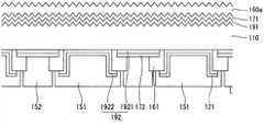
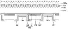
除了多个绝缘区161a的形成位置之外,图5中所示的太阳能电池12具有与图1和2中所示的太阳能电池11相同的结构。 The
更具体地说,太阳能电池12包括:顺序地位于基板110正面上的正面钝化层191、FSF区171和防反射层130;位于基板110背面上的背面钝化层192;位于背面钝化层192上的多个射极区121和多个BSF区172;位于多个射极区121和多个BSF区172上的多个第一辅助电极151和第二辅助电极152;位于多个第一辅助电极151和第二辅助电极152上的多个第一电极141和第二电极142;和位于彼此相邻的射极区121和BSF区172之间的多个绝缘区161a。 More specifically, the
按与图1和2中相同的方式,多个绝缘区161a位于基板110上,在相邻的第一背面钝化层1921和第二背面钝化层1922之间,在彼此相邻的射极区121和BSF区172之间,并且在相邻的BSF区172之间。 In the same manner as in FIGS. 1 and 2, a plurality of insulating
然而,不同于图1和2,各个绝缘区161a整个形成在各个BSF区172上,并且具有暴露各个BSF区172的一部分的多个开口181。各个开口181可以具有沿着BSF区172长延伸的条带形状,或彼此隔开的岛形状。当各个开口181具有岛形状时,各个开口181可以具有圆形、椭圆形或例如矩形的多边形的剖面形状。 However, unlike FIGS. 1 and 2 , each
换句话说,绝缘区161a基本上形成在BSF区172的整个表面上,除BSF区172的被多个开口181暴露的一部分之外。 In other words, the
因此,除了BSF区172的被开口181暴露的一部分之外,连接到BSF区172的第二辅助电极152还存在于BSF区172上的绝缘区161a上。因此,第二辅助电极152连接到BSF区172的被开口181暴露的一部分。换句话说,第二辅助电极152电子和物理地连接到BSF区172的一部分。 Accordingly, the second
上述太阳能电池12具有与太阳能电池11相同的效果。例如,因为绝缘区161a形成在彼此相邻的射极区121和BSF区172之间,所以在射极区121和BSF区172之间提供电绝缘。因此,防止了彼此相邻的射极 区121和BSF区172之间的短路和电气干扰。因此,改善了太阳能电池12的效率。 The
此外,因为绝缘区161a整个形成在BSF区172上,所以与图1和2相比,增加了绝缘区161a的形成面积。换句话说,由于绝缘区161a的形成面积的增加,钝化效应增大。此外,因为位于绝缘区161a之下的BSF区172和第一背面钝化层1921各自的厚度可以减小,所以降低了太阳能电池12的制造时间和制造成本。 In addition, since the
下面,参照图3A到3T、图4A和4B以及图6A和6B,描述根据本发明实施方式的太阳能电池12的制造方法。 Next, a method of manufacturing the
图6A和6B示出了图5中所示的太阳能电池12的制造方法的一部分。 6A and 6B show a part of the method of manufacturing the
如图3A到3M所示,在基板110的表面上形成粗糙表面,并且随后在基板110的正面和背面分别形成正面钝化层191和多个第一背面钝化层1921。在正面钝化层191和第一背面钝化层1921上分别形成FSF区171和多个BSF区172。随后,形成多个第二背面钝化层1922和多个射极区121。 As shown in FIGS. 3A to 3M , a rough surface is formed on the surface of the
接下来,如图3N所示,在基板110的整个背面上形成止蚀层73。随后,如图6A所示,将止蚀层73构图为与图3O中所示的图案不同的图案,从而部分地或选择性地暴露绝缘层160。接下来,如图6B所示,去除暴露的绝缘层160的一部分,以形成具有多个开口181的绝缘区161a。随后去除剩余的止蚀层73。 Next, as shown in FIG. 3N , an
因为随后的处理基本上与图3Q到3T或者图4A和4B中示出的处理相同,因此可以简短地进行进一步描述或者完全省略进一步描述。 Since subsequent processing is basically the same as the processing shown in FIGS. 3Q to 3T or FIGS. 4A and 4B , further description may be briefly made or completely omitted. the
下面参照图7描述根据本发明另一个实施方式的太阳能电池。 A solar cell according to another embodiment of the present invention is described below with reference to FIG. 7 . the
图7是根据本发明另一个实施方式的太阳能电池的部分剖面图; Figure 7 is a partial cross-sectional view of a solar cell according to another embodiment of the present invention;
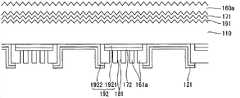
除了多个绝缘区161b的形成位置之外,图7中所示的太阳能电池13具有与图5中所示的太阳能电池12相同的结构。 The
更具体地说,太阳能电池13的多个绝缘区161b位于基板110上,在相邻的第一背面钝化层1921和第二背面钝化层1922之间,在彼此相 邻的射极区121和BSF区172之间,并且在相邻的BSF区172之间。此外,多个绝缘区161b部分地位于多个射极区121上。 More specifically, the plurality of insulating
在各个射极区121上的绝缘区161b主要位于各个射极区121的中央部分上。因此,绝缘区161b包括暴露BSF区172的一部分的多个开口181和暴露射极区121的一部分的多个开口182。按与开口181相同的方式,各个开口182可以具有条带形状或岛形状。 The
因此,第一辅助电极151位于对应的射极区121的暴露部分上,并且位于对应的射极区121上的绝缘区161b上。第二辅助电极152位于对应的BSF区172的暴露部分上,并且位于对应的BSF区172上的绝缘区161b上。如上所述,第一辅助电极151和第二辅助电极152彼此隔开。 Accordingly, the first
不同于图5,因为绝缘区161b位于射极区121的一部分上,所以由于绝缘区161b而进一步增加了钝化效应。此外,因为射极区121和第二背面钝化层1922各自的厚度以及位于绝缘区161b之下的BSF区172和第一背面钝化层1921各自的厚度都可以减小,所以进一步降低了太阳能电池13的制造时间和生产成本。此外,因为钝化效应的增加,所以增加了太阳能电池13的开路电压,并且,因为绝缘区161b之下的射极区121的厚度减少,所以降低了太阳能电池13的电阻。因此,增加了太阳能电池12的填充系数,并且进一步改善了太阳能电池12的效率。 Unlike FIG. 5, since the
下面,参照图3A到3T、图4A和4B、图8A到8C以及图9A到9D,描述根据本发明实施方式的太阳能电池13的制造方法。 Next, a method of manufacturing a
图8A到8C示出了图7中所示的太阳能电池13的制造方法的一部分。图9A到9D示出了图7中所示的太阳能电池13的另一制造方法的一部分。 8A to 8C show a part of the method of manufacturing
太阳能电池13的制造方法与图3A到3T以及图4A和4B中示出的太阳能电池11的制造方法类似。 The method of manufacturing
更具体地说,如图3A到3M所示,将正面钝化层191、FSF区171和第一绝缘层160a形成在基板110的粗糙正面上,并且将多个第一钝化层1921和多个BSF区172形成在基板110的背面上。此外,使用由与绝缘层160相同的材料形成的止蚀层72,将多个第二背面钝化层1922和多 个发射区121形成在基板110的背面上。 More specifically, as shown in FIGS. 3A to 3M, a
然而,不同于图3M,如图8A所示,再次将止蚀层74形成在剩余的止蚀层72和暴露的绝缘层160上。 However, unlike FIG. 3M , as shown in FIG. 8A , the
接下来,如图8B所示,去除止蚀层74的一部分,随后使用剩余的止蚀层74作为掩模,去除暴露的绝缘层160、和由与绝缘层160相同的材料形成的止蚀层72的暴露部分。如图8C所示,将具有多个第一开口181和第二开口182的绝缘层160b形成在彼此相邻的射极区121和BSF区172之间,形成在多个BSF区172上,并且形成在多个射极区121上。 Next, as shown in FIG. 8B , a part of the
如上所述,当止蚀层72由与绝缘层160相同的材料形成时,可以执行图8A到8C中示出的处理。 As described above, when the
因为随后的处理基本上与图3P到3T以及图4A和4B中示出的处理相同,因此可以简短地进行进一步描述或者完全省略进一步描述。 Since the subsequent processing is basically the same as the processing shown in FIGS. 3P to 3T and FIGS. 4A and 4B , further description may be briefly made or completely omitted. the
然而,当止蚀层72由不同于绝缘层160的材料形成时,通过图9A到9D中示出的处理来形成具有多个第一开口181和第二开口182的多个绝缘层160b。 However, when the
更具体地说,如图9A所示,在通过图3M中示出的处理来形成多个第二背面钝化层1922和多个射极区121之后,去除止蚀层72。随后,在基板110的整个背面上形成由与绝缘层160相同的材料形成的绝缘层160c。接下来,如图9B所示,去除绝缘层160c的一部分,并且在多个射极区121上保留绝缘层160c。 More specifically, as shown in FIG. 9A, after the plurality of second
接下来,如图9C所示,在基板110的整个背面上形成止蚀层76。接下来,如图9D所示,通过去除止蚀层76的一部分来形成具有期望图案的止蚀层76。 Next, as shown in FIG. 9C , an
随后,使用剩余的止蚀层76作为掩模,去除暴露的绝缘层160和160c,并且形成具有多个第一开口181和第二开口182的多个绝缘层160b(参照图8C)。因为随后的处理基本上与图3P到3T以及图4A和4B中示出的处理相同,因此可以简短地进行进一步描述或者完全省略进一步描述。 Subsequently, using the remaining
下面,参照图10到13描述根据本发明另一实施方式的各种太阳能 电池。 Next, various solar cells according to another embodiment of the present invention will be described with reference to FIGS. 10 to 13. the
当与图1、2、5和7中示出的太阳能电池进行比较时,图10到13中示出的根据本发明另一实施方式的太阳能电池的背面钝化层的形成位置不同。换句话说,与图1、2、5和7中示出的太阳能电池不同,除了基板110的整个背面之外,背面钝化层还位于彼此相邻的射极区和BSF区之间。 When compared with the solar cells shown in FIGS. 1 , 2 , 5 and 7 , the solar cells shown in FIGS. 10 to 13 according to another embodiment of the present invention have different formation positions of the rear passivation layer. In other words, unlike the solar cells shown in FIGS. 1 , 2 , 5 and 7 , in addition to the entire rear surface of the
图10是根据本发明另一个实施方式的太阳能电池的部分剖面图; Figure 10 is a partial cross-sectional view of a solar cell according to another embodiment of the present invention;
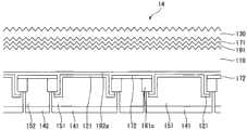
如图10所示,根据本发明另一个实施方式的太阳能电池14具有与图1和2中所示的太阳能电池11类似的结构。 As shown in FIG. 10 , a
当将图1、2、5和7中示出的太阳能电池与图10中所示的太阳能电池14进行比较时,背面钝化层192a的形成位置不同,并且,绝缘区161c的形成位置因为背面钝化层192a的形成位置的改变而改变。 When comparing the solar cells shown in FIGS. 1, 2, 5 and 7 with the
更具体地说,背面钝化层192a位于基板110的整个背面上,并且位于彼此相邻的射极区121和BSF区172之间。背面钝化层192a沿着平行于射极区121的方向在射极区121和BSF区172之间延伸,并且部分地与绝缘区161c的边缘交叠。 More specifically, the
如上所述,因为背面钝化层192a位于射极区121和BSF区172之间,所以如图10所示,绝缘区161c仅仅位于BSF区172上。此外,绝缘区161c沿着背面钝化层192a延伸。换句话说,绝缘区161c在与背面钝化层192a相邻的状态下延伸。 As described above, since the
因为除了背面钝化层192a和绝缘区161c的形成位置之外,图10中所示的太阳能电池14的结构与图1和2中所示的太阳能电池11基本上相同,所以可以简短地进行进一步描述或者完全省略进一步描述。 Since the structure of the
类似于图1和2中所示的太阳能电池11,因为由本征非晶硅形成且具有很大电阻率的背面钝化层192a除了位于基板110的背面之外还位于彼此相邻的射极区121和BSF区172之间,所以进一步改善了形成p-n结的射极区121和BSF区172之间的绝缘效果。因此,进一步防止了彼此相邻的射极区121和BSF区172之间的电气干扰。 Similar to the
此外,由于由具有优异钝化效应的非晶硅形成的背面钝化层192a的 缘故,大大改善了基板110的钝化效应,并且增加了太阳能电池14的开路电压。因此,进一步改善了太阳能电池14的效率。 In addition, the passivation effect of the
根据本发明另一个实施方式的太阳能电池14的制造方法几乎与图3A到3T或图4A和4B中示出的太阳能电池11的制造方法相同。 The method of manufacturing the
下面,参照图11A到11H以及图3A到3T或图4A和4B,描述太阳能电池14的制造方法。 Next, a method of manufacturing the
图11A到11H示出了图10中所示的太阳能电池13的制造方法的一部分。 11A to 11H show a part of the method of manufacturing
如图3A到3G所示,使用基板110背面上的绝缘层160a作为掩模,去除位于基板110背面的一部分上的BSF层170和第一背面钝化层190a,以形成多个背面钝化层1921。接下来,如图11A和11B所示,在不进行图3H和3I中示出的处理的情况下,使用PECVD方法等,在基板110的背面形成由与第一钝化层190a相同的材料(也就是本征非晶硅)形成的第二钝化层190b、以及由非晶硅形成的p型射极层120。 3A to 3G, using the insulating
接下来,按如图3K到3M所示的方式,去除发射极层120的一部分和第二钝化层190b的一部分。如图11C所示,形成多个射极区121和位于这些射极区121之下的多个第二背面钝化层192a。 Next, a portion of the
接下来,如图11D所示,按与图3N到3P同样的方式,在第二背面钝化层192a和BSF区172之间形成多个绝缘区161c。接下来,按如图3Q到3S或图4A和4B所示的方式,形成第一辅助电极151和第二辅助电极152以及第一电极141和第二电极142(参照图11E到11G)。然后,按如图3T所示的方式,在基板110的正面上形成防反射层130。如图11H所示,完成了太阳能电池14。 Next, as shown in FIG. 11D, a plurality of insulating
在太阳能电池14中,因为其中再次在第一钝化层190a上形成第二钝化层190b并且随后去除第二钝化层190b的一部分的处理不是必需的,所以简化了太阳能电池14的制造处理。 In the
图12是根据本发明另一个实施方式的太阳能电池的部分剖面图; 12 is a partial cross-sectional view of a solar cell according to another embodiment of the present invention;
除了背面钝化层192a的形成位置之外,图12中所示的太阳能电池15具有与图5中所示的太阳能电池12相同的结构。 Solar cell 15 shown in FIG. 12 has the same structure as
更具体地说,按与图10相同的方式,图12中所示的背面钝化层192a位于基板110的整个背面上并且位于彼此相邻的射极区121和BSF区172之间。背面钝化层192a按平行于射极区121的方向在射极区121和BSF区172之间延伸,并且部分地与绝缘区161d的边缘交叠。 More specifically, in the same manner as in FIG. 10, the
因此,绝缘区161d仅仅位于BSF区172上,并且具有如以上参照图5所述的多个开口181。 Therefore, the insulating region 161d is located only on the
因为除了背面钝化层192a和绝缘区161d各自的形成位置之外,图12中所示的太阳能电池15的结构与图5中所示的太阳能电池12基本上相同,所以可以简短进行进一步描述或者完全省略进一步描述。 Since the structure of the solar cell 15 shown in FIG. 12 is substantially the same as that of the
如以上参照图10所述,因为太阳能电池15的背面钝化层192a除了位于基板110的背面之外还位于彼此相邻的射极区121和BSF区172之间,所以进一步改善了射极区121和BSF区172之间的绝缘效果。因此,进一步防止了彼此相邻的射极区121和BSF区172之间的电气干扰。此外,按与图5中所示的太阳能电池12相同的方式,绝缘区161d完全位于各个BSF区172上,由于绝缘区161d的形成面积的增加而增加了钝化效应。此外,因为位于绝缘区161d之下的BSF区172和第一背面钝化层192a各自的厚度可以减少,所以降低了太阳能电池15的制造时间和制造成本。 As described above with reference to FIG. 10, since the
在太阳能电池15的制造方法中,按如图3A到3G和图11A到11C所示的方式,形成多个射极区121和背面钝化层192a。接下来,按如图6A和6B所示的方式,通过去除止蚀层73的一部分来形成图案,并且通过去除绝缘层160的一部分,在多个BSF区172上形成具有多个开口181的多个绝缘区161d。因为随后的处理基本上与按如图3Q到3T或者图4A和4B中示出的方式的形成第一辅助电极151和第二辅助电极152以及第一电极141和第二电极142的处理、以及在基板110的正面上形成防反射层130的处理相同,所以可以简短进行进一步描述或者完全省略进一步描述。 In the manufacturing method of the solar cell 15, a plurality of
图13是根据本发明另一个实施方式的太阳能电池的部分剖面图。 FIG. 13 is a partial cross-sectional view of a solar cell according to another embodiment of the present invention. the
除了背面钝化层192a的形成位置之外,图13中所示的太阳能电池 16具有与图7中所示的太阳能电池13相同的结构。 The
更具体地说,按与图10中相同的方式,图13中所示的背面钝化层192a位于基板110的整个背面上并且位于彼此相邻的射极区121和BSF区172之间。背面钝化层192a按平行于射极区121的方向在射极区121和BSF区172之间延伸,并且部分地与绝缘区161e的边缘交叠。 More specifically, in the same manner as in FIG. 10, the
因此,多个绝缘区161e仅仅位于BSF区172上和射极区121上,并且具有如以上参照图7所述的多个开口181和182。 Accordingly, the plurality of insulating
因为除了背面钝化层192a和绝缘区161e各自的形成位置之外,图13中所示的太阳能电池16的结构与图7中所示的太阳能电池13基本上相同,所以可以简短地进行进一步描述或者完全省略进一步描述。 Since the structure of the
因此,如以上参照图10所述,由于背面钝化层192a的缘故,射极区121和BSF区172之间的绝缘效果得到了进一步改善,并且进一步防止了彼此相邻的射极区121和BSF区172之间的电气干扰。 Therefore, as described above with reference to FIG. 10, due to the
此外,如图7所示,由于绝缘区161e的形成面积增加,所以降低了太阳能电池16的制造时间和制造成本。结果,太阳能电池16的效率得到进一步改善。 In addition, as shown in FIG. 7, since the formation area of the
在太阳能电池16的制造方法中,按图3A到3G和图11A到11C所示的方式,形成多个射极区121和多个背面钝化层192a。接下来,按图8A到8D或图9A到9D所示的方式,形成在多个BSF区172上具有多个第一开口181并且在多个射极区121上具有多个第二出口182的多个绝缘区161e。因为随后的处理基本上与按如图3Q到3T或者图4A和4B中示出的方式的形成第一辅助电极151和第二辅助电极152以及第一电极141和第二电极142的处理、以及在基板110的正面上形成防反射层130的处理相同,所以可以简短进行进一步描述或者完全省略进一步描述。 In the method of manufacturing the
如图10、12和13中描述的,多个第一辅助电极151和第二辅助电极152具有与位于这些第一辅助电极151和第二辅助电极152上的多个第一电极141和第二电极142相同的平面形状。然而,如上所述,根据形成电极141、142、151和152的方法,多个第一辅助电极151和第二 辅助电极152与位于第一辅助电极151和第二辅助电极152上的多个第一电极141和第二电极142可以具有不同的平面形状。 As described in FIGS. 10 , 12 and 13 , the plurality of first
下面参照图14到17描述根据本发明其它实施方式的各种太阳能电池。在下面的描述中,与图1到13中示出的结构和部件相同或等效的结构和部件采用相同的标号来表示,并且可以简短进行进一步描述或者完全省略进一步描述。 Various solar cells according to other embodiments of the present invention are described below with reference to FIGS. 14 to 17 . In the following description, the same or equivalent structures and components as those shown in FIGS. 1 to 13 are denoted by the same reference numerals, and further description may be briefly given or completely omitted. the
图14到图17是根据本发明其它实施方式的各种太阳能电池的部分横剖面图。 14 to 17 are partial cross-sectional views of various solar cells according to other embodiments of the present invention. the
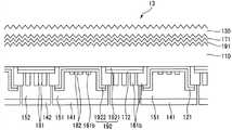
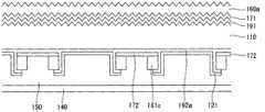
图14到17中所示的太阳能电池与图1到13中所示的太阳能电池的不同在于,具有均匀厚度的背面钝化层位于基板的整个背面上。 The solar cells shown in FIGS. 14 to 17 differ from the solar cells shown in FIGS. 1 to 13 in that a rear passivation layer having a uniform thickness is located on the entire rear surface of the substrate. the
图14中所示的太阳能电池17具有类似于图2和10中所示的太阳能电池的结构。 The
更具体地说,图14中所示的太阳能电池17包括:顺序地位于基板110正面上的正面钝化层191、FSF区171和防反射层130;位于基板110背面上的背面钝化层192b、多个射极区121和多个BSF区172;位于背面钝化层192b上在彼此相邻的射极区121和BSF区172之间、并且位于BSF区172的一部分上的多个绝缘区161;位于多个射极区121上并且位于绝缘区161的一部分上的多个第一辅助电极151;位于多个BSF区172上并且位于绝缘区161的一部分上的多个第二辅助电极152;位于多个第一辅助电极151上的多个第一电极141;以及位于多个第二辅助电极152上的多个第二电极142。 More specifically, the
在图14中所示的太阳能电池17中,与图10相比较,位于基板110整个背面上的背面钝化层192b具有基本均匀的厚度。在本例中,除了形状之外,背面钝化层192b的功能、材料等与图10中所示的背面钝化层192a基本相同。 In the
如图5所示,除了绝缘区161a部分地位于BSF区172上之外,图15中所示的太阳能电池18具有与图14中所示的太阳能电池17相同的结构。 As shown in FIG. 5, the
除了绝缘区161b部分地位于BSF区172上并且位于射极区121上之 外,图16中所示的太阳能电池19具有与图15中所示的太阳能电池18相同的结构。图16中所示的绝缘区161b的结构与图7的类似。 Solar cell 19 shown in FIG. 16 has the same structure as
在图14到16所示的太阳能电池17到19中,射极区121可以位于绝缘区161、161a或161b的与射极区121相邻的一部分上。 In the
此外,图14到16中所示的射极区121可以与图17中所示的射极区121a具有相同的形状。也就是说,图17中所示的射极区121a不与绝缘区161的侧边邻接,并且具有与BSF区172相同的形状。因此,与绝缘区161不同,图17中所示的绝缘区161f部分地位于与绝缘区161f相邻的射极区121a上,并且位于与绝缘区161f相邻的BSF区172上。 In addition, the
除了形成位置之外,绝缘区161f的功能、材料等基本上与绝缘区161相同。 The function, material, etc. of the
因为在图17中射极区121a不与绝缘区161f的侧边邻接,所以射极区121a可以比图14和15中所示的射极区121更容易地形成。因此,可以容易地制造图17中所示的太阳能电池20。 Since the
图14到17中所示的太阳能电池17到20与上述太阳能电池11到16中的至少一个具有相同的效果,并且通过一个叠加处理来形成图14到17中所示的背面钝化层192b。因此,可以容易地制造图14到17中所示的太阳能电池17到20。尤其是可以更容易地制造图17中所示的太阳能电池20。 The
在图14到17中,多个第一辅助电极151和第二辅助电极152具有与位于第一辅助电极151和第二辅助电极152上的多个第一电极141和第二电极142相同的平面形状。然而,如上所述,根据电极141、142、151和152的形成方法,多个第一辅助电极151和第二辅助电极152与位于第一辅助电极151和第二辅助电极152上的多个第一电极141和第二电极142可以具有不同的平面形状。 14 to 17, the plurality of first
虽然已参照多个示例性实施方式描述了实施方式,但应该理解,本领域技术人员能够设想落入本公开的原理的范围内的许多其它变型和实施方式。更具体地讲,在本公开、附图和所附权利要求的范围内,可以对主题组合设置的组成部件和/或设置进行各种变化和修改。除了对组成 部件和/或设置的各种变化和修改之外,另选用途对于本领域技术人员而言也是很明显的。 Although embodiments have been described with reference to a number of illustrative embodiments thereof, it should be understood that numerous other modifications and embodiments can be devised by those skilled in the art that will fall within the scope of the principles of this disclosure. More particularly, various changes and modifications may be made in the component parts and/or arrangements of the subject combination arrangement within the scope of the disclosure, drawings and appended claims. In addition to various changes and modifications to the component parts and/or arrangement, alternative uses will also be apparent to those skilled in the art. the
本申请要求于2009年9月7日和2010年5月11日在韩国知识产权局提交的韩国专利申请No.10-2009-0084046和No.10-2010-0043961的优先权和利益,在此通过引用并入其全部内容。 This application claims priority and the benefit of Korean Patent Applications No. 10-2009-0084046 and No. 10-2010-0043961 filed in the Korean Intellectual Property Office on Sep. 7, 2009 and May 11, 2010, hereby Its entire content is incorporated by reference. the
Claims (21)
Translated fromChineseApplications Claiming Priority (4)
| Application Number | Priority Date | Filing Date | Title |
|---|---|---|---|
| KR1020090084046AKR101135590B1 (en) | 2009-09-07 | 2009-09-07 | Solar cell and method for manufacturing the same |
| KR10-2009-0084046 | 2009-09-07 | ||
| KR10-2010-0043961 | 2010-05-11 | ||
| KR1020100043961AKR101141219B1 (en) | 2010-05-11 | 2010-05-11 | Solar cell and method for manufacturing the same |
Publications (2)
| Publication Number | Publication Date |
|---|---|
| CN102044579A CN102044579A (en) | 2011-05-04 |
| CN102044579Btrue CN102044579B (en) | 2013-12-18 |
Family
ID=43415248
Family Applications (1)
| Application Number | Title | Priority Date | Filing Date |
|---|---|---|---|
| CN2010105350624AActiveCN102044579B (en) | 2009-09-07 | 2010-09-07 | Solar cell |
Country Status (3)
| Country | Link |
|---|---|
| US (3) | US8525018B2 (en) |
| EP (1) | EP2293351B1 (en) |
| CN (1) | CN102044579B (en) |
Families Citing this family (51)
| Publication number | Priority date | Publication date | Assignee | Title |
|---|---|---|---|---|
| DE102008038184A1 (en)* | 2008-08-19 | 2010-02-25 | Suss Microtec Test Systems Gmbh | Method and device for the temporary electrical contacting of a solar cell |
| JP5213188B2 (en)* | 2010-04-27 | 2013-06-19 | シャープ株式会社 | Back electrode type solar cell and method of manufacturing back electrode type solar cell |
| KR101275575B1 (en)* | 2010-10-11 | 2013-06-14 | 엘지전자 주식회사 | Back contact solar cell and manufacturing method thereof |
| US20120167978A1 (en)* | 2011-01-03 | 2012-07-05 | Lg Electronics Inc. | Solar cell and method for manufacturing the same |
| WO2012132838A1 (en)* | 2011-03-25 | 2012-10-04 | 三洋電機株式会社 | Method for producing photoelectric conversion device |
| EP2690668A4 (en) | 2011-03-25 | 2014-09-03 | Sanyo Electric Co | METHOD FOR PRODUCING PHOTOELECTRIC CONVERSION ELEMENT |
| WO2012132995A1 (en) | 2011-03-25 | 2012-10-04 | 三洋電機株式会社 | Method for producing photoelectric conversion element |
| WO2012132835A1 (en)* | 2011-03-25 | 2012-10-04 | 三洋電機株式会社 | Solar cell |
| JPWO2012132766A1 (en)* | 2011-03-28 | 2014-07-28 | 三洋電機株式会社 | Photoelectric conversion device and method of manufacturing photoelectric conversion device |
| WO2012132729A1 (en)* | 2011-03-28 | 2012-10-04 | 三洋電機株式会社 | Photoelectric conversion device and method for producing same |
| KR101714780B1 (en) | 2011-06-08 | 2017-03-09 | 엘지전자 주식회사 | Solar cell module |
| CN102832116B (en)* | 2011-06-13 | 2015-03-25 | 聚日(苏州)科技有限公司 | Thin film strip structure, solar cell and manufacturing method of thin film strip structure |
| WO2013031298A1 (en)* | 2011-08-31 | 2013-03-07 | 三洋電機株式会社 | Solar cell module and method for producing same |
| US8889981B2 (en)* | 2011-10-18 | 2014-11-18 | Samsung Sdi Co., Ltd. | Photoelectric device |
| KR101826912B1 (en)* | 2011-11-07 | 2018-02-08 | 인텔렉츄얼 키스톤 테크놀로지 엘엘씨 | Photovoltaic device and the manufacturing methode thereof |
| KR20130050721A (en)* | 2011-11-08 | 2013-05-16 | 삼성에스디아이 주식회사 | Solar cell |
| KR101878397B1 (en)* | 2011-11-18 | 2018-07-16 | 인텔렉츄얼 키스톤 테크놀로지 엘엘씨 | Solar cell and method for fabricating the same |
| KR101863294B1 (en)* | 2011-11-25 | 2018-05-31 | 인텔렉츄얼 키스톤 테크놀로지 엘엘씨 | Solar cell and method for fabricating the same |
| US20130147003A1 (en) | 2011-12-13 | 2013-06-13 | Young-Su Kim | Photovoltaic device |
| JP2013125891A (en)* | 2011-12-15 | 2013-06-24 | Sharp Corp | Photoelectric conversion element and manufacturing method of the same |
| US8597970B2 (en)* | 2011-12-21 | 2013-12-03 | Sunpower Corporation | Hybrid polysilicon heterojunction back contact cell |
| CN104011881B (en)* | 2011-12-21 | 2016-05-04 | 太阳能公司 | Hybrid Polysilicon Heterojunction Back Contact Cell |
| US9054255B2 (en)* | 2012-03-23 | 2015-06-09 | Sunpower Corporation | Solar cell having an emitter region with wide bandgap semiconductor material |
| JP5906459B2 (en)* | 2012-03-30 | 2016-04-20 | パナソニックIpマネジメント株式会社 | Solar cell and manufacturing method thereof |
| KR101918738B1 (en)* | 2012-04-17 | 2018-11-15 | 엘지전자 주식회사 | Solar cell |
| JP2014072209A (en)* | 2012-09-27 | 2014-04-21 | Sharp Corp | Photoelectric conversion element and photoelectric conversion element manufacturing method |
| US20140102524A1 (en)* | 2012-10-15 | 2014-04-17 | Silevo, Inc. | Novel electron collectors for silicon photovoltaic cells |
| US8901010B2 (en)* | 2013-03-15 | 2014-12-02 | Sunpower Corporation | Methods for improving solar cell lifetime and efficiency |
| TWI509826B (en)* | 2013-10-09 | 2015-11-21 | Neo Solar Power Corp | Back contact solar cell and method of manufacturing same |
| US9196758B2 (en)* | 2013-12-20 | 2015-11-24 | Sunpower Corporation | Solar cell emitter region fabrication with differentiated p-type and n-type region architectures |
| JPWO2015189878A1 (en)* | 2014-06-13 | 2017-04-20 | 国立大学法人福島大学 | Solar cell and manufacturing method thereof |
| US10309012B2 (en) | 2014-07-03 | 2019-06-04 | Tesla, Inc. | Wafer carrier for reducing contamination from carbon particles and outgassing |
| KR20160064692A (en)* | 2014-11-28 | 2016-06-08 | 엘지전자 주식회사 | Solar cell and manufacturing method thereof |
| JP6564199B2 (en)* | 2015-02-18 | 2019-08-21 | シャープ株式会社 | Back electrode type photoelectric conversion element and method for manufacturing back electrode type photoelectric conversion element |
| US11355657B2 (en)* | 2015-03-27 | 2022-06-07 | Sunpower Corporation | Metallization of solar cells with differentiated p-type and n-type region architectures |
| US9525083B2 (en)* | 2015-03-27 | 2016-12-20 | Sunpower Corporation | Solar cell emitter region fabrication with differentiated P-type and N-type architectures and incorporating a multi-purpose passivation and contact layer |
| WO2017164099A1 (en)* | 2016-03-23 | 2017-09-28 | シャープ株式会社 | Photoelectric conversion device, photoelectric conversion module and solar photovoltaic power generation system |
| US20180138328A1 (en)* | 2016-11-11 | 2018-05-17 | Sunpower Corporation | Uv-curing of light-receiving surfaces of solar cells |
| WO2018168180A1 (en)* | 2017-03-17 | 2018-09-20 | 株式会社カネカ | Solar cell and method for manufacturing same |
| EP3664153A4 (en)* | 2017-09-13 | 2020-09-23 | Kaneka Corporation | SOLAR CELL, MANUFACTURING PROCESS FOR THE SOLAR CELL AND SOLAR CELL MODULE |
| US10672919B2 (en) | 2017-09-19 | 2020-06-02 | Tesla, Inc. | Moisture-resistant solar cells for solar roof tiles |
| KR101897168B1 (en)* | 2017-10-10 | 2018-09-12 | 엘지전자 주식회사 | Solar cell |
| US11190128B2 (en) | 2018-02-27 | 2021-11-30 | Tesla, Inc. | Parallel-connected solar roof tile modules |
| US11682744B2 (en)* | 2018-09-28 | 2023-06-20 | Maxeon Solar Pte. Ltd. | Solar cells having hybrid architectures including differentiated P-type and N-type regions |
| US11735678B2 (en)* | 2019-03-29 | 2023-08-22 | Maxeon Solar Pte. Ltd. | Solar cells having hybrid architectures including differentiated p-type and n-type regions with offset contacts |
| CN114365294B (en) | 2019-07-16 | 2024-03-26 | 株式会社钟化 | Solar cell and method for manufacturing solar cell |
| TWI748286B (en)* | 2019-11-21 | 2021-12-01 | 華邦電子股份有限公司 | Semiconductor device and method for forming the same |
| CN114497290A (en)* | 2022-02-10 | 2022-05-13 | 福建金石能源有限公司 | Manufacturing method of back contact heterojunction solar cell |
| CN115588698B (en)* | 2022-11-07 | 2024-11-01 | 隆基绿能科技股份有限公司 | Back contact solar cell, preparation method thereof and photovoltaic module |
| CN115832065B (en)* | 2022-11-29 | 2025-03-07 | 隆基绿能科技股份有限公司 | Back contact battery and manufacturing method thereof, photovoltaic module |
| CN116314415B (en)* | 2023-02-10 | 2024-09-27 | 天合光能股份有限公司 | Back contact solar cell and method of making same |
Citations (2)
| Publication number | Priority date | Publication date | Assignee | Title |
|---|---|---|---|---|
| CN101305472A (en)* | 2005-11-08 | 2008-11-12 | Lg化学株式会社 | High-efficiency solar cell and preparation method thereof |
| CN101401215A (en)* | 2006-01-26 | 2009-04-01 | 阿莱斯技术公司 | Solar battery |
Family Cites Families (32)
| Publication number | Priority date | Publication date | Assignee | Title |
|---|---|---|---|---|
| US6313397B1 (en)* | 1998-08-31 | 2001-11-06 | Sharp Kabushiki Kaisha | Solar battery cell |
| US6387726B1 (en)* | 1999-12-30 | 2002-05-14 | Sunpower Corporation | Method of fabricating a silicon solar cell |
| JP4244549B2 (en) | 2001-11-13 | 2009-03-25 | トヨタ自動車株式会社 | Photoelectric conversion element and manufacturing method thereof |
| JP2003298078A (en)* | 2002-03-29 | 2003-10-17 | Ebara Corp | Photovoltaic element |
| JP2004039751A (en)* | 2002-07-01 | 2004-02-05 | Toyota Motor Corp | Photovoltaic element |
| US7339110B1 (en)* | 2003-04-10 | 2008-03-04 | Sunpower Corporation | Solar cell and method of manufacture |
| US7388147B2 (en)* | 2003-04-10 | 2008-06-17 | Sunpower Corporation | Metal contact structure for solar cell and method of manufacture |
| CN100431177C (en)* | 2003-09-24 | 2008-11-05 | 三洋电机株式会社 | Photovoltaic element and manufacturing method thereof |
| KR100543532B1 (en) | 2003-10-24 | 2006-01-20 | 준 신 이 | Module integrated solar cell and its manufacturing method |
| EP1766690A1 (en)* | 2004-07-07 | 2007-03-28 | Saint-Gobain Glass France S.A. | Photovoltaic solar cell and solar module |
| US7554031B2 (en)* | 2005-03-03 | 2009-06-30 | Sunpower Corporation | Preventing harmful polarization of solar cells |
| DE102005019225B4 (en)* | 2005-04-20 | 2009-12-31 | Helmholtz-Zentrum Berlin Für Materialien Und Energie Gmbh | Heterocontact solar cell with inverted layer structure geometry |
| US7375378B2 (en)* | 2005-05-12 | 2008-05-20 | General Electric Company | Surface passivated photovoltaic devices |
| DE102005025125B4 (en)* | 2005-05-29 | 2008-05-08 | Hahn-Meitner-Institut Berlin Gmbh | Process for producing a solar cell contacted on one side and solar cell contacted on one side |
| US7468485B1 (en)* | 2005-08-11 | 2008-12-23 | Sunpower Corporation | Back side contact solar cell with doped polysilicon regions |
| KR100757797B1 (en) | 2006-02-03 | 2007-09-11 | 주식회사 실트론 | Method for manufacturing back electrode of single crystal solar cell |
| CN100411062C (en) | 2006-04-28 | 2008-08-13 | 泰兴市无氧铜材厂 | Copper-tin alloy contact wire for high-speed electrified railway and manufacturing method thereof |
| DE102006027737A1 (en)* | 2006-06-10 | 2007-12-20 | Hahn-Meitner-Institut Berlin Gmbh | Unilaterally contacted solar cell with plated-through holes and method of manufacture |
| US20080000522A1 (en) | 2006-06-30 | 2008-01-03 | General Electric Company | Photovoltaic device which includes all-back-contact configuration; and related processes |
| FR2906404B1 (en)* | 2006-09-21 | 2008-12-19 | Commissariat Energie Atomique | PROCESS FOR METALLIZING MULTIPLE RECOVERED PHOTOVOLTAIC CELLS |
| US20080173347A1 (en)* | 2007-01-23 | 2008-07-24 | General Electric Company | Method And Apparatus For A Semiconductor Structure |
| US7670638B2 (en)* | 2007-05-17 | 2010-03-02 | Sunpower Corporation | Protection layer for fabricating a solar cell |
| US8198528B2 (en)* | 2007-12-14 | 2012-06-12 | Sunpower Corporation | Anti-reflective coating with high optical absorption layer for backside contact solar cells |
| US20110000532A1 (en)* | 2008-01-30 | 2011-01-06 | Kyocera Corporation | Solar Cell Device and Method of Manufacturing Solar Cell Device |
| DE102008013446A1 (en)* | 2008-02-15 | 2009-08-27 | Ersol Solar Energy Ag | Process for producing monocrystalline n-silicon solar cells and solar cell, produced by such a process |
| US20090227095A1 (en)* | 2008-03-05 | 2009-09-10 | Nicholas Bateman | Counterdoping for solar cells |
| US20090227061A1 (en)* | 2008-03-05 | 2009-09-10 | Nicholas Bateman | Establishing a high phosphorus concentration in solar cells |
| WO2010025262A2 (en)* | 2008-08-27 | 2010-03-04 | Applied Materials, Inc. | Back contact solar cells using printed dielectric barrier |
| US20100051085A1 (en)* | 2008-08-27 | 2010-03-04 | Weidman Timothy W | Back contact solar cell modules |
| KR101002282B1 (en)* | 2008-12-15 | 2010-12-20 | 엘지전자 주식회사 | Solar cell and manufacturing method thereof |
| KR101142861B1 (en)* | 2009-02-04 | 2012-05-08 | 엘지전자 주식회사 | Solar cell and manufacturing method of the same |
| US8257995B2 (en)* | 2009-12-11 | 2012-09-04 | Twin Creeks Technologies, Inc. | Microwave anneal of a thin lamina for use in a photovoltaic cell |
- 2010
- 2010-09-07CNCN2010105350624Apatent/CN102044579B/enactiveActive
- 2010-09-07USUS12/876,821patent/US8525018B2/ennot_activeCeased
- 2010-09-07EPEP10009287.3Apatent/EP2293351B1/enactiveActive
- 2015
- 2015-09-02USUS14/843,778patent/USRE46515E1/enactiveActive
- 2017
- 2017-07-03USUS15/640,956patent/USRE47484E1/enactiveActive
Patent Citations (2)
| Publication number | Priority date | Publication date | Assignee | Title |
|---|---|---|---|---|
| CN101305472A (en)* | 2005-11-08 | 2008-11-12 | Lg化学株式会社 | High-efficiency solar cell and preparation method thereof |
| CN101401215A (en)* | 2006-01-26 | 2009-04-01 | 阿莱斯技术公司 | Solar battery |
Also Published As
| Publication number | Publication date |
|---|---|
| EP2293351A2 (en) | 2011-03-09 |
| USRE46515E1 (en) | 2017-08-15 |
| EP2293351B1 (en) | 2017-04-12 |
| USRE47484E1 (en) | 2019-07-02 |
| EP2293351A3 (en) | 2013-06-12 |
| US8525018B2 (en) | 2013-09-03 |
| CN102044579A (en) | 2011-05-04 |
| US20110056545A1 (en) | 2011-03-10 |
Similar Documents
| Publication | Publication Date | Title |
|---|---|---|
| CN102044579B (en) | Solar cell | |
| JP7564974B2 (en) | Photovoltaic cells and photovoltaic modules | |
| KR101142861B1 (en) | Solar cell and manufacturing method of the same | |
| US9508875B2 (en) | Solar cell and method for manufacturing the same | |
| CN102197495B (en) | Solar cell and manufacturing method thereof | |
| KR101918738B1 (en) | Solar cell | |
| US10680122B2 (en) | Solar cell and method for manufacturing the same | |
| CN102214709B (en) | Selective emitter solar cell | |
| CN103367478B (en) | Solaode and manufacture method thereof | |
| US20100218821A1 (en) | Solar cell and method for manufacturing the same | |
| CN103296093B (en) | Solaode and manufacture method thereof | |
| US20120118372A1 (en) | Solar cell | |
| CN103474482A (en) | Solar cell and method for manufacturing the same | |
| US9000291B2 (en) | Solar cell and method for manufacturing the same | |
| KR20120140049A (en) | Solar cell and method for manufacturing the same | |
| CN103943710B (en) | Solar cell and its manufacture method | |
| KR101898996B1 (en) | Silicon Solar Cell having Carrier Selective Contact | |
| KR101135590B1 (en) | Solar cell and method for manufacturing the same | |
| KR101897168B1 (en) | Solar cell | |
| KR101665139B1 (en) | Solar cell and method for manufacturing the same | |
| KR20120022008A (en) | Method for manufacturing solar cell | |
| KR101729310B1 (en) | Solar cell and method for manufacturing the same |
Legal Events
| Date | Code | Title | Description |
|---|---|---|---|
| C06 | Publication | ||
| PB01 | Publication | ||
| C10 | Entry into substantive examination | ||
| SE01 | Entry into force of request for substantive examination | ||
| C14 | Grant of patent or utility model | ||
| GR01 | Patent grant | ||
| EE01 | Entry into force of recordation of patent licensing contract | ||
| EE01 | Entry into force of recordation of patent licensing contract | Application publication date:20110504 Assignee:Hanhua thinksin Co.,Ltd. Assignor:LG ELECTRONICS Inc. Contract record no.:X2022990000645 Denomination of invention:Solar battery Granted publication date:20131218 License type:Common License Record date:20220914 | |
| TR01 | Transfer of patent right | ||
| TR01 | Transfer of patent right | Effective date of registration:20221101 Address after:No. 3, Yingbin Avenue, Shangrao Economic and Technological Development Zone, Jiangxi Province Patentee after:Shangrao Jingke Green Energy Technology Development Co.,Ltd. Address before:Seoul, South Kerean Patentee before:LG ELECTRONICS Inc. | |
| CP01 | Change in the name or title of a patent holder | ||
| CP01 | Change in the name or title of a patent holder | Address after:No. 3, Yingbin Avenue, Shangrao Economic and Technological Development Zone, Jiangxi Province 334100 Patentee after:Shangrao Xinyuan Yuedong Technology Development Co.,Ltd. Address before:No. 3, Yingbin Avenue, Shangrao Economic and Technological Development Zone, Jiangxi Province 334100 Patentee before:Shangrao Jingke Green Energy Technology Development Co.,Ltd. |