CN102043547A - Display device having optical sensing frame and method for detecting touch using the same - Google Patents
Display device having optical sensing frame and method for detecting touch using the sameDownload PDFInfo
- Publication number
- CN102043547A CN102043547ACN2010105302495ACN201010530249ACN102043547ACN 102043547 ACN102043547 ACN 102043547ACN 2010105302495 ACN2010105302495 ACN 2010105302495ACN 201010530249 ACN201010530249 ACN 201010530249ACN 102043547 ACN102043547 ACN 102043547A
- Authority
- CN
- China
- Prior art keywords
- light
- retroreflector
- display device
- optical fiber
- display panel
- Prior art date
- Legal status (The legal status is an assumption and is not a legal conclusion. Google has not performed a legal analysis and makes no representation as to the accuracy of the status listed.)
- Granted
Links
Images


Classifications
- G—PHYSICS
- G06—COMPUTING OR CALCULATING; COUNTING
- G06F—ELECTRIC DIGITAL DATA PROCESSING
- G06F3/00—Input arrangements for transferring data to be processed into a form capable of being handled by the computer; Output arrangements for transferring data from processing unit to output unit, e.g. interface arrangements
- G06F3/01—Input arrangements or combined input and output arrangements for interaction between user and computer
- G06F3/03—Arrangements for converting the position or the displacement of a member into a coded form
- G06F3/041—Digitisers, e.g. for touch screens or touch pads, characterised by the transducing means
- G06F3/042—Digitisers, e.g. for touch screens or touch pads, characterised by the transducing means by opto-electronic means
- G06F3/0421—Digitisers, e.g. for touch screens or touch pads, characterised by the transducing means by opto-electronic means by interrupting or reflecting a light beam, e.g. optical touch-screen
- G—PHYSICS
- G02—OPTICS
- G02B—OPTICAL ELEMENTS, SYSTEMS OR APPARATUS
- G02B6/00—Light guides; Structural details of arrangements comprising light guides and other optical elements, e.g. couplings
- G02B6/10—Light guides; Structural details of arrangements comprising light guides and other optical elements, e.g. couplings of the optical waveguide type
- G02B6/12—Light guides; Structural details of arrangements comprising light guides and other optical elements, e.g. couplings of the optical waveguide type of the integrated circuit kind
- G02B6/122—Basic optical elements, e.g. light-guiding paths
- G—PHYSICS
- G06—COMPUTING OR CALCULATING; COUNTING
- G06F—ELECTRIC DIGITAL DATA PROCESSING
- G06F3/00—Input arrangements for transferring data to be processed into a form capable of being handled by the computer; Output arrangements for transferring data from processing unit to output unit, e.g. interface arrangements
- G06F3/01—Input arrangements or combined input and output arrangements for interaction between user and computer
- G06F3/03—Arrangements for converting the position or the displacement of a member into a coded form
- G06F3/033—Pointing devices displaced or positioned by the user, e.g. mice, trackballs, pens or joysticks; Accessories therefor
- G06F3/0354—Pointing devices displaced or positioned by the user, e.g. mice, trackballs, pens or joysticks; Accessories therefor with detection of 2D relative movements between the device, or an operating part thereof, and a plane or surface, e.g. 2D mice, trackballs, pens or pucks
- G—PHYSICS
- G06—COMPUTING OR CALCULATING; COUNTING
- G06F—ELECTRIC DIGITAL DATA PROCESSING
- G06F3/00—Input arrangements for transferring data to be processed into a form capable of being handled by the computer; Output arrangements for transferring data from processing unit to output unit, e.g. interface arrangements
- G06F3/01—Input arrangements or combined input and output arrangements for interaction between user and computer
- G06F3/03—Arrangements for converting the position or the displacement of a member into a coded form
- G06F3/041—Digitisers, e.g. for touch screens or touch pads, characterised by the transducing means
- G06F3/0412—Digitisers structurally integrated in a display
- G—PHYSICS
- G06—COMPUTING OR CALCULATING; COUNTING
- G06F—ELECTRIC DIGITAL DATA PROCESSING
- G06F3/00—Input arrangements for transferring data to be processed into a form capable of being handled by the computer; Output arrangements for transferring data from processing unit to output unit, e.g. interface arrangements
- G06F3/01—Input arrangements or combined input and output arrangements for interaction between user and computer
- G06F3/03—Arrangements for converting the position or the displacement of a member into a coded form
- G06F3/041—Digitisers, e.g. for touch screens or touch pads, characterised by the transducing means
- G06F3/0416—Control or interface arrangements specially adapted for digitisers
- G06F3/04166—Details of scanning methods, e.g. sampling time, grouping of sub areas or time sharing with display driving
- Y—GENERAL TAGGING OF NEW TECHNOLOGICAL DEVELOPMENTS; GENERAL TAGGING OF CROSS-SECTIONAL TECHNOLOGIES SPANNING OVER SEVERAL SECTIONS OF THE IPC; TECHNICAL SUBJECTS COVERED BY FORMER USPC CROSS-REFERENCE ART COLLECTIONS [XRACs] AND DIGESTS
- Y10—TECHNICAL SUBJECTS COVERED BY FORMER USPC
- Y10T—TECHNICAL SUBJECTS COVERED BY FORMER US CLASSIFICATION
- Y10T29/00—Metal working
- Y10T29/49—Method of mechanical manufacture
- Y10T29/49826—Assembling or joining
Landscapes
- Engineering & Computer Science (AREA)
- General Engineering & Computer Science (AREA)
- Theoretical Computer Science (AREA)
- Physics & Mathematics (AREA)
- General Physics & Mathematics (AREA)
- Human Computer Interaction (AREA)
- Microelectronics & Electronic Packaging (AREA)
- Optics & Photonics (AREA)
- Position Input By Displaying (AREA)
Abstract
Description
Translated fromChinese本申请要求享有2009年10月22日提交的韩国专利申请No.10-2009-0100588的权益,在此引入该申请以供参考。This application claims the benefit of Korean Patent Application No. 10-2009-0100588 filed on Oct. 22, 2009, which is incorporated herein by reference.
技术领域technical field
本发明涉及一种显示设备,特别涉及一种具有光传感框架(frame)的显示设备,在该光传感框架中采用具有包括光接收层和光发射层的双层结构的波导管单元以实现结构简化以及增加有效面积,以及涉及一种使用该显示设备检测触摸的方法。The present invention relates to a display device, in particular to a display device having a light sensing frame in which a waveguide unit having a double-layer structure including a light receiving layer and a light emitting layer is used to realize It simplifies the structure and increases the effective area, and relates to a touch detection method using the display device.
背景技术Background technique
一般来讲,触摸面板构成了在使用各种显示器的信息和通信设备与用户之间的界面。触摸面板是一种通过用手或笔直接接触屏幕来与一装置进行接口连接的输入装置。触摸面板是一种可以通过以用户的手指接触在显示器上显示的按钮来进行操作的输入装置。因此,触摸面板容易被所有年龄的用户来使用。触摸面板被用于各种应用中,包括银行或者政府机关中的信息发布机器、各种医疗设备、电子导游、以及电子交通向导。In general, a touch panel constitutes an interface between an information and communication device using various displays and a user. A touch panel is an input device that interfaces with a device by directly touching the screen with a hand or a pen. A touch panel is an input device that can be operated by touching buttons displayed on a display with a user's finger. Therefore, the touch panel is easy to use by users of all ages. The touch panel is used in various applications including information distribution machines in banks or government agencies, various medical equipment, electronic guides, and electronic traffic guides.
根据感测触摸的方式,触摸面板被划分为电阻型触摸面板、微电容型触摸面板(玻璃)、超声波型触摸面板(玻璃)、红外线型触摸面板等等。Touch panels are classified into a resistive type touch panel, a micro capacitive type touch panel (glass), an ultrasonic type touch panel (glass), an infrared type touch panel, etc., according to a way of sensing a touch.
首先,电阻型触摸面板由两个导电透明层,即由涂覆有导电材料的玻璃或塑料制成的下层以及由涂覆有导电材料的膜制成的上层组成。通过微印刷的间隔垫,这两个层被电气隔离开预定距离。根据这种电阻型触摸面板,当将预定电压施加到涂覆有导电材料的两个层上,并用手或笔触摸上板时,上板(X轴)和下板(Y轴)经受到取决于触摸放置的电阻变化,设置于其中的控制器计算经受到电阻变化的上板(X轴)和下板(Y轴)的位置,以显示出屏幕上的X和Y坐标,由此可以通过触摸屏输入数据。First, a resistive touch panel consists of two conductive transparent layers, a lower layer made of glass or plastic coated with a conductive material and an upper layer made of a film coated with a conductive material. The two layers are electrically separated by a predetermined distance by microprinted spacers. According to this resistive touch panel, when a predetermined voltage is applied to the two layers coated with a conductive material, and the upper plate is touched with a hand or a pen, the upper plate (X axis) and the lower plate (Y axis) undergo a Due to the resistance change of the touch placement, the controller disposed therein calculates the positions of the upper plate (X axis) and the lower plate (Y axis) subjected to the resistance change to display the X and Y coordinates on the screen, which can be passed through Touch screen to enter data.
微电容型触摸面板包括薄薄地涂覆有导电材料的透明玻璃传感器。导电涂层包括沿着该导电涂层的边缘精细印刷的电极图案。此外,与导电层的上侧紧密接触地涂有由透明玻璃制成的防护涂覆膜,以保护和包围该玻璃传感器。微电容型触摸面板在工作时将预定电压施加到玻璃屏幕上,电极图案通过所述导电层在触摸传感器的表面上形成低压电场。因此,当用户用他或她的手指触摸屏幕时,在触摸部分产生微安培数的电流。此外,由于来自每一角落的电流与从该角落到手指的距离成比例,因此触摸屏控制器可以通过使用该电流的安培数进行成比例的计算来确定该触摸部分。A micro-capacitive touch panel includes a transparent glass sensor thinly coated with a conductive material. The conductive coating includes finely printed electrode patterns along edges of the conductive coating. Furthermore, a protective coating film made of transparent glass is coated in close contact with the upper side of the conductive layer to protect and surround the glass sensor. When the micro-capacitive touch panel is in operation, a predetermined voltage is applied to the glass screen, and the electrode pattern forms a low-voltage electric field on the surface of the touch sensor through the conductive layer. Therefore, when a user touches the screen with his or her finger, a current of microamperes is generated in the touched portion. Furthermore, since the current from each corner is proportional to the distance from the corner to the finger, the touch screen controller can determine the touched portion by performing a proportional calculation using the amperage of the current.
超声波型触摸面板完全由玻璃制成。因此,与可能由于表面上的极小擦伤或磨损而减小寿命的其他触摸屏相比,超声波型触摸面板不受表面损伤或磨损的影响。此外,在超声波型触摸面板中,触摸屏控制器将5MHz电信号发送到产生超声波的发射换能器。随后通过反射线,使所产生的超声波穿过面板表面。因此,当用户触摸触摸屏的表面时,穿过触摸部分的一部分超声波被用户吸收,信号损失通过所接收的信号和数字地图被发送到控制器。然后,控制器计算其中发生信号变化的部分的坐标值。上述一系列操作是相对于X轴和Y轴独立地执行的。Ultrasonic touch panels are made entirely of glass. Therefore, ultrasonic touch panels are not affected by surface damage or wear compared to other touch screens that may have a reduced lifespan due to minimal scratches or wear on the surface. Also, in an ultrasonic type touch panel, the touch screen controller sends a 5MHz electrical signal to a transmitting transducer that generates ultrasonic waves. The generated ultrasonic waves are then passed through the panel surface by means of reflected lines. Therefore, when the user touches the surface of the touch screen, part of the ultrasonic wave passing through the touched part is absorbed by the user, and the signal loss is sent to the controller through the received signal and digital map. Then, the controller calculates the coordinate value of the portion where the signal change occurs. The series of operations described above are independently performed with respect to the X-axis and the Y-axis.
红外型触摸面板使用红外线的直线效应(straightness effect),也就是使用红外线不会前行越过置于射线前方的障碍物的原理。更详细来讲,沿水平和垂直方向发射的红外线在用户触摸的部分受到阻碍,控制器确定红外线受阻处的X轴和Y轴的坐标值。因此,红外型触摸面板通过红外线在触摸面板的正面发生的中断,来检测触摸部分。此外,红外线从X轴和Y轴的一侧射出,而在X轴和Y轴的另一侧被接收,从而形成一个不可见的红外线矩阵。Infrared touch panels use the straightness effect of infrared rays, that is, the principle that infrared rays will not move forward and cross obstacles placed in front of the rays. In more detail, the infrared rays emitted along the horizontal and vertical directions are blocked at the part touched by the user, and the controller determines coordinate values of the X-axis and the Y-axis where the infrared rays are blocked. Therefore, the infrared type touch panel detects a touched portion by interruption of infrared rays occurring on the front surface of the touch panel. In addition, infrared rays are emitted from one side of the X-axis and Y-axis and received on the other side of the X-axis and Y-axis, thus forming an invisible infrared matrix.
尽管如上所述,每种类型的面板都具有不同的优点,但是红外型触摸面板目前非常受关注,因为它们只需要对触摸面板施加较小的压力。接下来,将参照附图说明现有技术的红外型触摸面板。Although each type of panel has different advantages as mentioned above, infrared type touch panels are currently attracting much attention because they require less pressure to be applied to the touch panel. Next, a related art infrared type touch panel will be described with reference to the drawings.
图1是示出根据现有技术的红外型触摸面板的平面图。FIG. 1 is a plan view illustrating an infrared type touch panel according to the related art.
如图1中所示,如上所述,现有技术的红外型触摸面板形成了红外线(IR)矩阵、在与触摸面板表面相邻的两边设有光发射波导管10的光发射部19、以及在另外的相邻两边设有光接收波导管16的光接收部20。As shown in FIG. 1, as described above, the infrared type touch panel of the related art forms an infrared (IR) matrix, a
光发射部19和光接收部20分别具有与光发射波导管10和光接收波导管16相连接的透镜12和15,用于将经由各自的波导管发射和接收的光笔直地传送到矩阵。光发射部19的光发射波导管10被设置在具有用于向其传送光的LED光源11以及分光器18的一侧。光接收部20被设置在具有光传感器17的一侧,光传感器17与光接收波导管16相连接,用于检测触摸的存在性。在这里,光传感器17具有用于判定用户的触摸坐标的光传感器阵列,这是因为光传感器17与光接收波导管16连接,而光接收波导管16与X轴和Y轴两者连接。The
在这样一种结构中,光发射部19和光接收部20分别被设置在具有光源11和光传感器17的一侧。为了将光源11和光传感器17连接到波导管10和16以便沿X轴和Y轴方向传送光,不可避免地必须增加远离光源11和光传感器17的波导管的线路长度以及光发射部19和光接收部20的面积。In such a structure, the
上述的现有技术红外型触摸面板具有几个缺点。首先,应当将具有波导管和透镜的光发射部或光接收部布置在触摸面板平面的四个边上。为了感测触摸,应当在触摸面板的所有边缘上设置所有构造。因此,元件位置复杂,并且线路长度增加。由于这些缺点,由显示设备产生的电噪声或EMI会影响触摸系统。其次,应当在相邻两边设置光接收部和光发射部,这使得结构复杂,并有效面积减少。第三,随着触摸面板面积的增加,像素数目也增加了,需要更多的波导管和透镜。具有预定尺寸的触摸面板的有效面积减小。在其各两边设有光发射部和光接收部的触摸面板不会体现布置在下部区域中的显示面板的有效面积效率。结果,现有技术的红外型触摸面板不适用于大面积的显示设备。此外,由于触摸模块的体积,目前趋于薄边框的趋势也抑制了集成有触摸模块的显示器的实现。The prior art infrared type touch panels described above have several disadvantages. First, a light emitting section or a light receiving section having a waveguide and a lens should be arranged on the four sides of the touch panel plane. In order to sense touch, all formations should be provided on all edges of the touch panel. Therefore, component positions are complicated, and the line length is increased. Due to these disadvantages, electrical noise or EMI generated by the display device can affect the touch system. Secondly, the light receiving part and the light emitting part should be arranged on adjacent two sides, which makes the structure complicated and reduces the effective area. Third, as the area of the touch panel increases, the number of pixels also increases, requiring more waveguides and lenses. The effective area of the touch panel having a predetermined size is reduced. A touch panel provided with a light emitting portion and a light receiving portion on each of its two sides does not exhibit the effective area efficiency of a display panel disposed in a lower region. As a result, the related art infrared type touch panel is not suitable for a large-area display device. In addition, the current trend toward thin bezels also inhibits the realization of displays integrated with touch modules due to the volume of the touch modules.
发明内容Contents of the invention
据此,本发明旨在提供一种具有光传感框架的显示设备以及使用该显示设备检测触摸的方法,其基本上避免了由于现有技术的局限性和不足而引起的一个或多个问题。Accordingly, the present invention is directed to a display device having a light sensing frame and a method of detecting touch using the same, which substantially obviate one or more problems due to limitations and deficiencies of the related art .
本发明的一个目的是提供一种改进的具有光传感框架的显示设备,以及使用该显示设备检测触摸的方法。An object of the present invention is to provide an improved display device having a light sensing frame, and a method of detecting a touch using the display device.
本发明的另一目的是提供一种改进的可增加有效面积的具有光传感框架的显示设备,以及使用该显示设备检测触摸的方法。Another object of the present invention is to provide an improved display device with a photo-sensing frame that can increase the effective area, and a method of detecting a touch using the display device.
本发明的额外的特征和优点,一部分将在随后的说明书中阐述,一部分根据本说明书将是明显的,或者可以通过本发明的实践而被了解。可以通过在书面说明书及其权利要求书以及所附附图中具体指明的结构来实现和获得本发明的目的及其他优点。Additional features and advantages of the invention will be set forth in the description which follows, and in part will be obvious from the description, or may be learned by practice of the invention. The objectives and other advantages of the invention may be realized and attained by the structure particularly pointed out in the written description and claims hereof as well as the appended drawings.
为了实现这些目的及其他优点、并根据本发明的目的,正如此处所具体实现和概括描述的,一种具有光传感框架的显示设备包括:显示面板;布置在所述显示面板的两个相邻边上的至少一个波导管单元,所述波导管单元具有叠层结构,该叠层结构包括光发射层和用于接收反射光的光接收层;以及布置在与所述波导管单元相对的边上的多个回射器。In order to achieve these objects and other advantages, and according to the object of the present invention, as embodied and generally described herein, a display device with a light sensing frame includes: a display panel; At least one waveguide unit on the adjacent side, the waveguide unit has a laminated structure including a light emitting layer and a light receiving layer for receiving reflected light; and the waveguide unit is arranged opposite to the waveguide unit Multiple retroreflectors on the side.
根据本发明的另一方面,一种用于制造具有光传感框架的显示设备的方法包括以下步骤:提供显示面板;提供布置在所述显示面板的两个相邻边上的至少一个波导管单元,所述波导管单元具有叠层结构,该叠层结构包括光发射层和用于接收反射光的光接收层;以及提供布置在与所述波导管单元相对的边上的多个回射器。According to another aspect of the present invention, a method for manufacturing a display device having a light sensing frame comprises the steps of: providing a display panel; providing at least one waveguide arranged on two adjacent sides of said display panel A unit having a laminated structure including a light emitting layer and a light receiving layer for receiving reflected light; and providing a plurality of retroreflective device.
根据本发明的又一方面,一种检测对具有光传感框架的显示设备的触摸的方法,所述方法包括以下步骤:准备该显示设备,使该显示设备具有显示面板、布置在所述显示面板的相邻两个边上的波导管单元、布置在所述显示面板的剩余两个边上的回射器、以及用于包围所述显示面板、所述波导管单元和所述回射器的外壳,其中所述波导管单元具有叠层结构,该叠层结构包括用于发射红外光的光发射层和用于接收反射光并由此检测触摸的光接收层;使用输入部触摸所述显示面板的一部分;以及使所述波导管单元感测由触摸部分中的所述输入部的介入而引起的反射光的接收量的变化,并使所述输入部阻挡发射光以防止回射,由此检测触摸的存在性及触摸位置。According to yet another aspect of the present invention, a method of detecting a touch on a display device having a light-sensing frame, the method comprising the steps of: preparing the display device, making the display device have a display panel, arranged on the display The waveguide unit on the two adjacent sides of the panel, the retroreflector arranged on the remaining two sides of the display panel, and the display panel, the waveguide unit and the retroreflector wherein the waveguide unit has a laminated structure including a light-emitting layer for emitting infrared light and a light-receiving layer for receiving reflected light and thereby detecting touch; touch the a part of the display panel; and causing the waveguide unit to sense a change in the received amount of reflected light caused by the intervention of the input part in the touch part, and causing the input part to block the emitted light to prevent retroreflection, In this way, the presence of touch and the touch position are detected.
应理解的是,本发明的上述概括说明及随后的详细说明都是示例性的和解释性的,旨在为所请求保护的本发明提供进一步的解释。It is to be understood that both the foregoing general description and the following detailed description of the present invention are exemplary and explanatory and are intended to provide further explanation of the invention as claimed.
附图说明Description of drawings
附图包括在本申请中以提供对于本发明的进一步的理解,它们被并入并构成本申请的一部分,附图示出本发明的实施方式并与说明书一起用于解释本发明的原理。在附图中:The accompanying drawings, which are included to provide a further understanding of the invention and are incorporated in and constitute a part of this application, illustrate embodiments of the invention and together with the description serve to explain the principle of the invention. In the attached picture:
图1是示出根据现有技术的红外型触摸面板的平面图;FIG. 1 is a plan view illustrating an infrared type touch panel according to the related art;
图2是示出根据本发明的具有光传感框架的示例性显示设备的平面图;2 is a plan view illustrating an exemplary display device with a light sensing frame according to the present invention;
图3是示出图2的示例性显示设备的剖视图;3 is a cross-sectional view illustrating the exemplary display device of FIG. 2;
图4是示出图2的示例性波导管单元的透视图;FIG. 4 is a perspective view illustrating the exemplary waveguide unit of FIG. 2;
图5是示出图2的示例性回射器(retroreflector)单元的剖视图;5 is a cross-sectional view illustrating the exemplary retroreflector unit of FIG. 2;
图6是示出图2的示例性回射器单元的顶视图;6 is a top view showing the exemplary retroreflector unit of FIG. 2;
图7是示出图5的示例性回射器单元的示例性滤光器的透射率的图表;以及7 is a graph showing the transmittance of an example filter of the example retroreflector unit of FIG. 5; and
图8是示出根据本发明的包括光传感框架的示例性液晶显示装置的剖视图。FIG. 8 is a cross-sectional view illustrating an exemplary liquid crystal display device including a light sensing frame according to the present invention.
具体实施方式Detailed ways
现在将详细参考本发明的实施方式进行描述,附图中示出了这些实施方式的范例。在下文中,将参考附图说明根据本发明的具有光传感框架的显示设备以及使用该显示设备检测触摸的方法。Reference will now be made in detail to embodiments of the invention, examples of which are illustrated in the accompanying drawings. Hereinafter, a display device having a light sensing frame and a method of detecting a touch using the display device according to the present invention will be explained with reference to the accompanying drawings.
图2是示出根据本发明的具有光传感框架的示例性显示设备的平面图。图3是示出图2的示例性显示设备的剖视图。FIG. 2 is a plan view illustrating an exemplary display device having a light sensing frame according to the present invention. FIG. 3 is a cross-sectional view illustrating the exemplary display device of FIG. 2 .
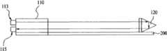
如图2和3中所示,具有光传感框架的显示设备100包括具有四个平边的矩形结构的显示面板200,布置在显示面板200的相邻两边上的波导管单元110,其具有包括发射红外光的光发射层(由图4中的附图标记“111”表示)和接收反射光并检测触摸的光接收层(由图4中的附图标记″112″表示)的叠层结构;布置在显示面板200的剩余两边上的回射器单元120;以及包围显示面板200、波导管单元110和回射器单元120的外壳(未示出)。根据需要,光发射层111和光接收层112可以以颠倒的位置来堆叠,也可以每个都独立地具有包括两个或更多层的叠层结构。As shown in FIGS. 2 and 3 , a
上述光传感框架是指用于光学感测光强度的框架。在本发明中,光传感框架包括波导管单元和回射器,并且光传感框架围绕显示面板。The aforementioned light sensing frame refers to a frame for optically sensing light intensity. In the present invention, the light sensing frame includes a waveguide unit and a retroreflector, and the light sensing frame surrounds the display panel.
如图2中所示,光在沿着X和Y轴方向上的多个部分中从波导管单元110中笔直射出。回射器单元120又沿相反方向将所接收的光反射。也就是说,回射器单元120接收笔直的光,使得该光能够被笔直地传输到波导管单元。As shown in FIG. 2 , light is straightly emitted from the
当通过一物体触摸具有光传感框架的显示设备100的预定部分时,由于吸光率、散射或反射等原因,该物体阻挡了笔直光在相应部分中的通路。因此,阻止所接收的光传输到回射器。波导管单元110确定光的接收及其变化。从而检测到该触摸的存在性及其对应位置。When a predetermined portion of the
图4是示出图2的示例性波导管单元的透视图。FIG. 4 is a perspective view illustrating an exemplary waveguide unit of FIG. 2 .
如图4中所示,波导管单元110包括光发射层111和光接收层112,并依次向该光发射层111和该光接收层112照射光。优选地,光发射层111包括第一多条光纤,光接收层112包括第二多条光纤,从光发射层的光纤发射出的光被光接收层的对应光纤接收,并且优选地,第一多条光纤中的每一条与第一类型的光学透镜连接,第二多条光纤中的每一条与第二类型的光学透镜连接;优选地,所述第一类型的光学透镜是聚光光学透镜,第二类型的光学透镜是窄视角光学透镜。特别是,波导管单元110的光发射层111被设置在具有用于发射红外光的红外LED 113、用于分配从红外LED113发射出的光的分光器(未示出)和多条光纤114的一边上,所述光纤114用于使得所分配的来自红外LED113的光能够在多个部分中向X和Y轴笔直传输。As shown in FIG. 4 , the
波导管单元110的光接收层112包括用于接收从回射器单元120反射的光的多条光纤116,以及与光纤116的一端连接以利用从光纤116传输来的光检测触摸的存在性的作为光检测器的至少一个线型光传感器115。此外,还可以与显示面板200的布置有光纤116和114的边相邻地设置光效率透镜。The light-receiving
图5是示出图2的示例性回射器单元的剖视图。图8是示出根据本发明的包括光传感框架的示例性液晶显示装置的剖视图。FIG. 5 is a cross-sectional view illustrating the exemplary retroreflector unit of FIG. 2 . FIG. 8 is a cross-sectional view illustrating an exemplary liquid crystal display device including a light sensing frame according to the present invention.
优选地,回射器单元120包括:滤光器层,用于去除来自除了光发射层之外的源的光;以及回射器棱镜层,用于反射从所述光发射层接收的光。具体地,如图5中所示,回射器单元120包括用于仅透射红外线的滤光器121、用于反射所接收的光的回射器123、和插入到滤光器121和回射器123之间以粘合滤光器121和回射器123的第一粘合层122。此外,回射器单元120还包括布置在回射器123下方的第二粘合层124。在第二粘合层124中,在其具有用于支撑回射器单元120的线型支撑件(图8的180)的内侧设置了外壳所使用的壳顶部(图8中的185)。此外,回射器单元120可以被粘附到支撑件180的一侧。优选地,在波导管单元和显示面板之间设置第一支撑件,在回射器单元和显示面板之间设置第二支撑件。Preferably, the
图6是示出图2的示例性回射器的顶视图。如图6中所示,回射器123具有立方折角的形式,类似微棱镜。在0到65度范围之内的光角度具有优异的回射效率。FIG. 6 is a top view illustrating the exemplary retroreflector of FIG. 2 . As shown in FIG. 6, the retroreflector 123 has the form of a cube corner, similar to a microprism. Excellent retroreflection efficiency for light angles in the range of 0 to 65 degrees.
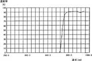
图7是示出图5的示例性回射器单元的示例性滤光器的透射率的图表。FIG. 7 is a graph showing the transmittance of an example filter of the example retroreflector unit of FIG. 5 .
如图7中所示,滤光器121仅仅透射红外线之上的光,而阻挡剩余的可见光之上的光。可以采用黑色材料(可见光吸收材料),以便阻挡可见光。例如,滤光器121可以具有大约700nm的截止频率。As shown in FIG. 7, the filter 121 transmits only light above infrared rays and blocks the remaining light above visible rays. A black material (visible light absorbing material) may be used in order to block visible light. For example, the filter 121 may have a cutoff frequency of about 700 nm.
滤光器121可以由丙烯酸树脂制成。例如,该丙烯酸树脂可以是聚甲基丙烯酸甲酯(PMMA)或者聚碳酸酯。可选地,滤光器121可以包含玻璃。The filter 121 may be made of acrylic resin. For example, the acrylic resin may be polymethyl methacrylate (PMMA) or polycarbonate. Optionally, the filter 121 may contain glass.
同时,用于具有光传感框架的显示设备的显示面板可以选自于液晶面板、PDP面板、有机发光显示面板和电泳面板。液晶面板在其下部区域具有附加的光源。Meanwhile, a display panel for a display device having a light sensing frame may be selected from a liquid crystal panel, a PDP panel, an organic light emitting display panel, and an electrophoretic panel. The liquid crystal panel has an additional light source in its lower area.
这种显示设备需要包围显示面板200、布置在显示面板200外围的波导管单元110和回射器单元120的材料。此外,波导管单元110和回射器单元120也可以包括在外壳内。Such a display device requires materials surrounding the
例如,当显示面板是包括第一基板、第二基板以及填充在它们之间的液晶层的液晶面板时,提供了框架型壳顶部185,其覆盖该液晶面板的外围和侧部。该显示面板包括壳顶部185,用于遮蔽布置在液晶面板外围的波导管单元110和回射器单元120。For example, when the display panel is a liquid crystal panel including a first substrate, a second substrate, and a liquid crystal layer filled therebetween, a frame-
在这里,回射器单元120被粘附到壳顶部185的一内侧,波导管单元110被粘附到或者在结构上被插入到壳顶部185的另一内侧中,以实现集成结构。具有包括光发射层111和光接收层112的双层叠层结构的波导管单元110被应用于显示面板的两个相邻边,回射器被应用于其剩余的两边(即与波导管单元相对的边),从而在不增加非有效面积的情况下将光传感框架集成到显示模块中。Here, the
特别是,回射器仅仅由膜或者粘合层组成,而没有任何反射透镜、线或元件。因此,与波导管单元相比,能够显著地减小回射器的宽度,并且其厚度能够减少到1,000μm或者更少。由于这个缘故,回射器对于纤薄显示设备很有用。结果,能够实现无边结构。In particular, the retroreflector consists only of films or adhesive layers without any reflective lenses, wires or elements. Therefore, compared with the waveguide unit, the width of the retroreflector can be significantly reduced, and its thickness can be reduced to 1,000 μm or less. For this reason, retroreflectors are useful for slim display devices. As a result, a borderless structure can be realized.
此外,包括光发射层111和光接收层112的双层叠层结构的波导管单元是有益的,这是因为,分别连接到光发射层111和光接收层112的红外LED和线型光传感器能够被容易地设置在每一块中,并且该波导管单元对于大型显示设备很有用。例如,线型光传感器被设置在包括与其分辨率对应的像素的每一块中。此外,红外LED的位置可以被设置为将红外LED的发光效率和反射效率(其中回射器单元120对从LED接收的光进行反射)保持在预定级别。In addition, a waveguide unit including a two-layer laminated structure of the light-emitting
液晶显示装置以如下方式感测触摸。在波导管单元110的光发射部111中提供的红外LED 113发射红外光,回射器单元120将该红外光回射到相对侧,以便将光传送到波导管单元110的光接收部112,从而使光接收部112的线型光传感器115能够感测到反射和传送的光。此时,当通过输入部比如手或者笔来触摸该设备时,由于输入装置或部位的介入,发射和反射的光的传输在对应部分被阻挡。因此,通过感测从线型光传感器115中读出的反射光的接收量的变化,可以判断触摸的存在性、光量发生变化的部分、以及作为触摸部分通过光纤连接的对应位置(X和Y坐标)。也就是说,波导管单元110根据输入装置或部位在触摸区域中的固有反射率来感测由各个元件产生的吸收光、散射光以及反射光的变化,并阻挡由输入装置或部位发出的光以防止回射,由此能够感测触摸的存在性及触摸区域。The liquid crystal display device senses a touch as follows. The
根据本发明的具有光传感框架的显示设备具有以下优点。首次,具有包括光接收层和光发射层的双层叠层结构的波导管单元被应用于显示面板的两个相邻边,回射器单元被应用于其剩余的两边,以将光传感框架集成到显示模块中。第二,回射器被应用于显示面板的面向波导管的边上,而没有将任何反射透镜应用到波导管上,因此不再需要使用任何反射透镜和与之连接的元件,简化了用于触摸感测的结构。第三,在大型显示设备的情况中,可以将显示面板划分成多个块,并可以将红外LED和线型光传感器设置到每一块中。线型光传感器感测到发射光的回射,或者触摸物阻挡了发射光从而阻止光传送到回射器。因此,可以通过感测光是否未被传输到回射器单元以及若未被传输到回射器单元则不会发生回射来检测触摸的存在性。因此,显示面板对于大型显示设备很有用。第四,与其中在光接收部和光发射部中分开提供波导管、透镜和传感器或者光源的现有技术显示设备相比,本发明的显示设备将波导管单元应用到显示面板的两个边,并将具有简单结构的回射器应用到其剩余的两边,其仅仅使用了光学元件,而未设置任何电子线路,因此简化了仪器设计,缩小了存在于光传感框架边缘的仪器的面积,并最终实现了具有接近无边结构的显示设备。第五,降低了连接到波导管的透镜的数目,减小了制造成本。The display device with the light sensing frame according to the present invention has the following advantages. For the first time, a waveguide unit with a double-layer laminate structure including a light-receiving layer and a light-emitting layer was applied to two adjacent sides of a display panel, and a retroreflector unit was applied to its remaining two sides to integrate the light-sensing frame into the display module. Second, the retroreflector is applied to the side of the display panel facing the waveguide without applying any reflective lens to the waveguide, so there is no need to use any reflective lens and components connected thereto, simplifying the use of The structure of touch sensing. Third, in the case of a large display device, the display panel may be divided into a plurality of blocks, and an infrared LED and a line-type light sensor may be provided into each block. The line light sensor senses the retroreflection of the emitted light, or a touching object blocks the emitted light preventing the light from being transmitted to the retroreflector. Accordingly, the presence of a touch may be detected by sensing whether light is not transmitted to the retroreflector unit, and if not transmitted to the retroreflector unit, retroreflection does not occur. Therefore, the display panel is useful for a large display device. Fourth, compared to the prior art display device in which waveguides, lenses, and sensors or light sources are separately provided in the light receiving part and the light emitting part, the display device of the present invention applies waveguide units to both sides of the display panel, And applying the retroreflector with simple structure to its remaining two sides, which only uses optical elements without setting any electronic circuit, thus simplifying the instrument design and reducing the area of the instrument existing at the edge of the light sensing frame, And finally a display device with a nearly edgeless structure is realized. Fifth, the number of lenses connected to the waveguide is reduced, reducing manufacturing costs.
对于所属领域中技术人员清楚明白的是,可以对本发明的具有光传感框架的显示设备及使用该显示设备检测触摸的方法作出各种修改和变动,而不会脱离本发明的精神或范围。因此,本发明意在涵盖对本发明的所有修改和变动,只要这些修改和变动落入所附权利要求书范围及其等效范围之内。It will be apparent to those skilled in the art that various modifications and changes can be made to the display device with a light sensing frame and the method for detecting touch using the display device of the present invention without departing from the spirit or scope of the present invention. Thus, it is intended that the present invention cover all modifications and variations of this invention provided they come within the scope of the appended claims and their equivalents.
Claims (25)
Applications Claiming Priority (2)
| Application Number | Priority Date | Filing Date | Title |
|---|---|---|---|
| KR10-2009-0100588 | 2009-10-22 | ||
| KR1020090100588AKR101352117B1 (en) | 2009-10-22 | 2009-10-22 | Display device having touch panel and touch sensing method thereof |
Publications (2)
| Publication Number | Publication Date |
|---|---|
| CN102043547Atrue CN102043547A (en) | 2011-05-04 |
| CN102043547B CN102043547B (en) | 2014-03-19 |
Family
ID=43909724
Family Applications (1)
| Application Number | Title | Priority Date | Filing Date |
|---|---|---|---|
| CN201010530249.5AExpired - Fee RelatedCN102043547B (en) | 2009-10-22 | 2010-10-21 | Display device having optical sensing frame and method for detecting touch using the same |
Country Status (3)
| Country | Link |
|---|---|
| US (1) | US8624876B2 (en) |
| KR (1) | KR101352117B1 (en) |
| CN (1) | CN102043547B (en) |
Cited By (5)
| Publication number | Priority date | Publication date | Assignee | Title |
|---|---|---|---|---|
| CN102722293A (en)* | 2012-06-05 | 2012-10-10 | 北京理工大学 | High-resolution-ratio infrared touch screen |
| CN102750047A (en)* | 2012-06-05 | 2012-10-24 | 北京理工大学 | Infrared touch screen positioning method based on optical fibers |
| CN103920598A (en)* | 2013-01-15 | 2014-07-16 | 北京华德创业环保设备有限公司 | Conversion method device for foam flotation camera gray image and analog quantity |
| WO2015043293A1 (en)* | 2013-09-30 | 2015-04-02 | 京东方科技集团股份有限公司 | Optical touch control screen and display device |
| CN107678601A (en)* | 2010-12-13 | 2018-02-09 | 三星电子株式会社 | For sensing multiconductor and the display device close to object |
Families Citing this family (17)
| Publication number | Priority date | Publication date | Assignee | Title |
|---|---|---|---|---|
| US8711125B2 (en)* | 2010-02-04 | 2014-04-29 | Hong Kong Applied Science And Technology Research Institute Co. Ltd. | Coordinate locating method and apparatus |
| US8937612B2 (en)* | 2010-02-04 | 2015-01-20 | Hong Kong Applied Science And Technology Research Institute Co. Ltd. | Coordinate locating method, coordinate locating device, and display apparatus comprising the coordinate locating device |
| KR101159179B1 (en)* | 2010-10-13 | 2012-06-22 | 액츠 주식회사 | Touch screen system and manufacturing method thereof |
| CA2819551C (en)* | 2010-12-01 | 2017-10-10 | Smart Technologies Ulc | Multi-touch input system with re-direction of radiation |
| US20120169671A1 (en)* | 2011-01-03 | 2012-07-05 | Primax Electronics Ltd. | Multi-touch input apparatus and its interface method using data fusion of a single touch sensor pad and an imaging sensor |
| US20120327029A1 (en)* | 2011-06-27 | 2012-12-27 | Qualcomm Mems Technologies, Inc. | Touch input sensing using optical ranging |
| CN102967892B (en)* | 2011-08-30 | 2015-12-02 | 原相科技股份有限公司 | Reflector for optical touch device and optical touch device using same |
| CN103827792A (en)* | 2011-09-29 | 2014-05-28 | 英特尔公司 | Optical fiber proximity sensor |
| TWI451312B (en)* | 2011-12-19 | 2014-09-01 | Pixart Imaging Inc | Optical touch device and light source assembly |
| KR102092944B1 (en) | 2013-10-23 | 2020-03-25 | 삼성디스플레이 주식회사 | Touch screen panel and detecting method of touch position using the same |
| KR102233188B1 (en) | 2014-10-29 | 2021-03-30 | 삼성디스플레이 주식회사 | Display device |
| EP3344433B1 (en)* | 2015-08-31 | 2020-01-29 | Uniplas Enterprises PTE Ltd | Injection moulding apparatus and method for injection moulding and ir-compatible display frame |
| US10169630B2 (en) | 2015-12-03 | 2019-01-01 | Synaptics Incorporated | Optical sensor for integration over a display backplane |
| US10176355B2 (en) | 2015-12-03 | 2019-01-08 | Synaptics Incorporated | Optical sensor for integration in a display |
| US9934418B2 (en) | 2015-12-03 | 2018-04-03 | Synaptics Incorporated | Display integrated optical fingerprint sensor with angle limiting reflector |
| CN105786267B (en)* | 2016-02-19 | 2019-04-02 | 京东方科技集团股份有限公司 | Photosensitive reflecting mirror, laser induced touch device and laser touch control detecting method |
| US10613269B2 (en)* | 2016-07-01 | 2020-04-07 | Intel Corporation | Stacked light wave guides for display panels |
Citations (3)
| Publication number | Priority date | Publication date | Assignee | Title |
|---|---|---|---|---|
| CN1794157A (en)* | 2005-12-29 | 2006-06-28 | 广东威创日新电子有限公司 | Infrared touch device |
| CN201233592Y (en)* | 2008-08-05 | 2009-05-06 | 北京汇冠新技术有限公司 | Reflective light path construction used for infrared touch screen |
| CN101546239A (en)* | 2008-03-24 | 2009-09-30 | 日东电工株式会社 | Device using waveguide, optical touch panel, and method of manufacturing waveguide |
Family Cites Families (15)
| Publication number | Priority date | Publication date | Assignee | Title |
|---|---|---|---|---|
| JPH0325220Y2 (en)* | 1985-02-15 | 1991-05-31 | ||
| JP2574780B2 (en)* | 1986-12-26 | 1997-01-22 | オムロン株式会社 | Reflective photoelectric switch |
| US5914709A (en)* | 1997-03-14 | 1999-06-22 | Poa Sana, Llc | User input device for a computer system |
| DE19806288A1 (en)* | 1998-02-16 | 1999-08-26 | Fraunhofer Ges Forschung | Laser scanner measuring system |
| KR20000018260A (en)* | 2000-01-27 | 2000-04-06 | 김시호 | An Apparatus for inputting positions of Coordinate |
| JP3881148B2 (en)* | 2000-02-18 | 2007-02-14 | 株式会社リコー | Photodetection device for coordinate detection, coordinate input / detection device, electronic blackboard, mounting position detection method, and storage medium |
| US6992659B2 (en)* | 2001-05-22 | 2006-01-31 | Palmone, Inc. | High transparency integrated enclosure touch screen assembly for a portable hand held device |
| JP2004127073A (en)* | 2002-10-04 | 2004-04-22 | Smk Corp | Instruction input device |
| US7450799B2 (en)* | 2006-01-24 | 2008-11-11 | Uni-Pixel Displays, Inc. | Corner-cube retroreflectors for displays |
| US20080106527A1 (en)* | 2006-11-06 | 2008-05-08 | Rpo Pty Limited | Waveguide Configurations for Minimising Substrate Area |
| JP4864761B2 (en)* | 2007-02-19 | 2012-02-01 | 日東電工株式会社 | Optical waveguide for touch panel |
| US8842366B2 (en)* | 2007-05-11 | 2014-09-23 | Zetta Research and Development LLC—RPO Series | Transmissive body |
| WO2010048679A1 (en)* | 2008-10-31 | 2010-05-06 | Rpo Pty Limited | A transmissive body |
| US8659561B2 (en)* | 2009-12-18 | 2014-02-25 | Lg Display Co., Ltd. | Display device including optical sensing frame and method of sensing touch |
| CN102270069B (en)* | 2010-06-03 | 2015-01-28 | 乐金显示有限公司 | Touch panel integrated display device |
- 2009
- 2009-10-22KRKR1020090100588Apatent/KR101352117B1/ennot_activeExpired - Fee Related
- 2010
- 2010-10-21CNCN201010530249.5Apatent/CN102043547B/ennot_activeExpired - Fee Related
- 2010-10-21USUS12/909,388patent/US8624876B2/ennot_activeExpired - Fee Related
Patent Citations (3)
| Publication number | Priority date | Publication date | Assignee | Title |
|---|---|---|---|---|
| CN1794157A (en)* | 2005-12-29 | 2006-06-28 | 广东威创日新电子有限公司 | Infrared touch device |
| CN101546239A (en)* | 2008-03-24 | 2009-09-30 | 日东电工株式会社 | Device using waveguide, optical touch panel, and method of manufacturing waveguide |
| CN201233592Y (en)* | 2008-08-05 | 2009-05-06 | 北京汇冠新技术有限公司 | Reflective light path construction used for infrared touch screen |
Cited By (9)
| Publication number | Priority date | Publication date | Assignee | Title |
|---|---|---|---|---|
| CN107678601A (en)* | 2010-12-13 | 2018-02-09 | 三星电子株式会社 | For sensing multiconductor and the display device close to object |
| CN107678601B (en)* | 2010-12-13 | 2021-05-18 | 三星电子株式会社 | Display device for sensing multiple contacts and proximity objects |
| CN102722293A (en)* | 2012-06-05 | 2012-10-10 | 北京理工大学 | High-resolution-ratio infrared touch screen |
| CN102750047A (en)* | 2012-06-05 | 2012-10-24 | 北京理工大学 | Infrared touch screen positioning method based on optical fibers |
| CN102722293B (en)* | 2012-06-05 | 2014-12-31 | 北京理工大学 | High-resolution-ratio infrared touch screen |
| CN102750047B (en)* | 2012-06-05 | 2015-01-21 | 北京理工大学 | Infrared touch screen positioning method based on optical fibers |
| CN103920598A (en)* | 2013-01-15 | 2014-07-16 | 北京华德创业环保设备有限公司 | Conversion method device for foam flotation camera gray image and analog quantity |
| WO2015043293A1 (en)* | 2013-09-30 | 2015-04-02 | 京东方科技集团股份有限公司 | Optical touch control screen and display device |
| US10139939B2 (en) | 2013-09-30 | 2018-11-27 | Boe Technology Group Co., Ltd. | Optical touch screen and display device |
Also Published As
| Publication number | Publication date |
|---|---|
| KR20110043872A (en) | 2011-04-28 |
| US20110254809A1 (en) | 2011-10-20 |
| KR101352117B1 (en) | 2014-01-14 |
| US8624876B2 (en) | 2014-01-07 |
| CN102043547B (en) | 2014-03-19 |
Similar Documents
| Publication | Publication Date | Title |
|---|---|---|
| CN102043547A (en) | Display device having optical sensing frame and method for detecting touch using the same | |
| US8659561B2 (en) | Display device including optical sensing frame and method of sensing touch | |
| CN102096526B (en) | Optical sensing unit, display module and display device using optical sensing unit | |
| CN102103441B (en) | Method for detecting touch and optical touch sensing system | |
| JP5101702B2 (en) | Coordinate sensor, electronic equipment, display device, light receiving unit | |
| CN102109933B (en) | Assembly having display panel and optical sensing frame and display system using the same | |
| EP2339438B1 (en) | Optical touch input system and method of establishing reference in the same | |
| TW201510823A (en) | Optical touch panel and touch display panel | |
| US20100214269A1 (en) | Optical touch module | |
| US20150205442A1 (en) | Optical touch screen | |
| KR101715851B1 (en) | Optical Sensing Unit, Display Module and Display Device Using the Same | |
| CN102662527A (en) | Touch Sensing Display Device | |
| JP2022511133A (en) | In-screen fingerprint identification device and electronic devices | |
| KR101735393B1 (en) | Display Device having Optical Sensing Frame and Method Detecting Multi-Touch Using the Same | |
| KR101351420B1 (en) | Display Device Including Optical Sensing Frame | |
| CN110869838A (en) | Display device with integrated optically operated proximity sensor system | |
| KR101308477B1 (en) | Method for Detecting Touch and Display Device Using the Same | |
| KR100868824B1 (en) | Optical touch screen | |
| KR20110075723A (en) | Touch Sensitivity Compensation Method for the Touch Assembly Integrated Display | |
| KR101706236B1 (en) | Display device using optical sensing unit | |
| KR101735397B1 (en) | Optical Touch Input Device and Method for Manufacturing the Same | |
| KR20120051218A (en) | Optical touch input device | |
| KR20120071142A (en) | Optical sensing unit and image display device using the same |
Legal Events
| Date | Code | Title | Description |
|---|---|---|---|
| C06 | Publication | ||
| PB01 | Publication | ||
| C10 | Entry into substantive examination | ||
| SE01 | Entry into force of request for substantive examination | ||
| GR01 | Patent grant | ||
| GR01 | Patent grant | ||
| CF01 | Termination of patent right due to non-payment of annual fee | Granted publication date:20140319 Termination date:20181021 | |
| CF01 | Termination of patent right due to non-payment of annual fee |