CN102037717B - Image capture and image processing using monolithic camera arrays with heterogeneous imagers - Google Patents
Image capture and image processing using monolithic camera arrays with heterogeneous imagersDownload PDFInfo
- Publication number
- CN102037717B CN102037717BCN2009801178901ACN200980117890ACN102037717BCN 102037717 BCN102037717 BCN 102037717BCN 2009801178901 ACN2009801178901 ACN 2009801178901ACN 200980117890 ACN200980117890 ACN 200980117890ACN 102037717 BCN102037717 BCN 102037717B
- Authority
- CN
- China
- Prior art keywords
- camera
- camera array
- filter
- imager
- array
- Prior art date
- Legal status (The legal status is an assumption and is not a legal conclusion. Google has not performed a legal analysis and makes no representation as to the accuracy of the status listed.)
- Active
Links
Images


Classifications
- H—ELECTRICITY
- H04—ELECTRIC COMMUNICATION TECHNIQUE
- H04N—PICTORIAL COMMUNICATION, e.g. TELEVISION
- H04N23/00—Cameras or camera modules comprising electronic image sensors; Control thereof
- H04N23/90—Arrangement of cameras or camera modules, e.g. multiple cameras in TV studios or sports stadiums
- H—ELECTRICITY
- H04—ELECTRIC COMMUNICATION TECHNIQUE
- H04N—PICTORIAL COMMUNICATION, e.g. TELEVISION
- H04N23/00—Cameras or camera modules comprising electronic image sensors; Control thereof
- H04N23/50—Constructional details
- H04N23/55—Optical parts specially adapted for electronic image sensors; Mounting thereof
- G—PHYSICS
- G02—OPTICS
- G02B—OPTICAL ELEMENTS, SYSTEMS OR APPARATUS
- G02B13/00—Optical objectives specially designed for the purposes specified below
- G02B13/001—Miniaturised objectives for electronic devices, e.g. portable telephones, webcams, PDAs, small digital cameras
- G02B13/0015—Miniaturised objectives for electronic devices, e.g. portable telephones, webcams, PDAs, small digital cameras characterised by the lens design
- G—PHYSICS
- G02—OPTICS
- G02B—OPTICAL ELEMENTS, SYSTEMS OR APPARATUS
- G02B13/00—Optical objectives specially designed for the purposes specified below
- G02B13/001—Miniaturised objectives for electronic devices, e.g. portable telephones, webcams, PDAs, small digital cameras
- G02B13/0085—Miniaturised objectives for electronic devices, e.g. portable telephones, webcams, PDAs, small digital cameras employing wafer level optics
- G—PHYSICS
- G02—OPTICS
- G02B—OPTICAL ELEMENTS, SYSTEMS OR APPARATUS
- G02B27/00—Optical systems or apparatus not provided for by any of the groups G02B1/00 - G02B26/00, G02B30/00
- G02B27/0025—Optical systems or apparatus not provided for by any of the groups G02B1/00 - G02B26/00, G02B30/00 for optical correction, e.g. distorsion, aberration
- G—PHYSICS
- G02—OPTICS
- G02B—OPTICAL ELEMENTS, SYSTEMS OR APPARATUS
- G02B27/00—Optical systems or apparatus not provided for by any of the groups G02B1/00 - G02B26/00, G02B30/00
- G02B27/10—Beam splitting or combining systems
- G02B27/1066—Beam splitting or combining systems for enhancing image performance, like resolution, pixel numbers, dual magnifications or dynamic range, by tiling, slicing or overlapping fields of view
- G—PHYSICS
- G02—OPTICS
- G02B—OPTICAL ELEMENTS, SYSTEMS OR APPARATUS
- G02B27/00—Optical systems or apparatus not provided for by any of the groups G02B1/00 - G02B26/00, G02B30/00
- G02B27/10—Beam splitting or combining systems
- G02B27/12—Beam splitting or combining systems operating by refraction only
- G02B27/123—The splitting element being a lens or a system of lenses, including arrays and surfaces with refractive power
- G—PHYSICS
- G02—OPTICS
- G02B—OPTICAL ELEMENTS, SYSTEMS OR APPARATUS
- G02B3/00—Simple or compound lenses
- G02B3/0006—Arrays
- G—PHYSICS
- G02—OPTICS
- G02B—OPTICAL ELEMENTS, SYSTEMS OR APPARATUS
- G02B5/00—Optical elements other than lenses
- G02B5/20—Filters
- G—PHYSICS
- G02—OPTICS
- G02B—OPTICAL ELEMENTS, SYSTEMS OR APPARATUS
- G02B5/00—Optical elements other than lenses
- G02B5/20—Filters
- G02B5/208—Filters for use with infrared or ultraviolet radiation, e.g. for separating visible light from infrared and/or ultraviolet radiation
- G—PHYSICS
- G06—COMPUTING OR CALCULATING; COUNTING
- G06T—IMAGE DATA PROCESSING OR GENERATION, IN GENERAL
- G06T1/00—General purpose image data processing
- G06T1/20—Processor architectures; Processor configuration, e.g. pipelining
- G—PHYSICS
- G06—COMPUTING OR CALCULATING; COUNTING
- G06T—IMAGE DATA PROCESSING OR GENERATION, IN GENERAL
- G06T3/00—Geometric image transformations in the plane of the image
- G06T3/40—Scaling of whole images or parts thereof, e.g. expanding or contracting
- G06T3/4053—Scaling of whole images or parts thereof, e.g. expanding or contracting based on super-resolution, i.e. the output image resolution being higher than the sensor resolution
- G—PHYSICS
- G06—COMPUTING OR CALCULATING; COUNTING
- G06T—IMAGE DATA PROCESSING OR GENERATION, IN GENERAL
- G06T7/00—Image analysis
- G06T7/50—Depth or shape recovery
- G—PHYSICS
- G06—COMPUTING OR CALCULATING; COUNTING
- G06T—IMAGE DATA PROCESSING OR GENERATION, IN GENERAL
- G06T7/00—Image analysis
- G06T7/50—Depth or shape recovery
- G06T7/55—Depth or shape recovery from multiple images
- G—PHYSICS
- G06—COMPUTING OR CALCULATING; COUNTING
- G06T—IMAGE DATA PROCESSING OR GENERATION, IN GENERAL
- G06T7/00—Image analysis
- G06T7/50—Depth or shape recovery
- G06T7/55—Depth or shape recovery from multiple images
- G06T7/557—Depth or shape recovery from multiple images from light fields, e.g. from plenoptic cameras
- G—PHYSICS
- G06—COMPUTING OR CALCULATING; COUNTING
- G06T—IMAGE DATA PROCESSING OR GENERATION, IN GENERAL
- G06T7/00—Image analysis
- G06T7/70—Determining position or orientation of objects or cameras
- H—ELECTRICITY
- H04—ELECTRIC COMMUNICATION TECHNIQUE
- H04N—PICTORIAL COMMUNICATION, e.g. TELEVISION
- H04N1/00—Scanning, transmission or reproduction of documents or the like, e.g. facsimile transmission; Details thereof
- H04N1/04—Scanning arrangements, i.e. arrangements for the displacement of active reading or reproducing elements relative to the original or reproducing medium, or vice versa
- H04N1/19—Scanning arrangements, i.e. arrangements for the displacement of active reading or reproducing elements relative to the original or reproducing medium, or vice versa using multi-element arrays
- H04N1/195—Scanning arrangements, i.e. arrangements for the displacement of active reading or reproducing elements relative to the original or reproducing medium, or vice versa using multi-element arrays the array comprising a two-dimensional array or a combination of two-dimensional arrays
- H04N1/19589—Optical means, e.g. an optical fibre bundle, for mapping the whole or a part of a scanned image onto the array
- H—ELECTRICITY
- H04—ELECTRIC COMMUNICATION TECHNIQUE
- H04N—PICTORIAL COMMUNICATION, e.g. TELEVISION
- H04N1/00—Scanning, transmission or reproduction of documents or the like, e.g. facsimile transmission; Details thereof
- H04N1/04—Scanning arrangements, i.e. arrangements for the displacement of active reading or reproducing elements relative to the original or reproducing medium, or vice versa
- H04N1/19—Scanning arrangements, i.e. arrangements for the displacement of active reading or reproducing elements relative to the original or reproducing medium, or vice versa using multi-element arrays
- H04N1/195—Scanning arrangements, i.e. arrangements for the displacement of active reading or reproducing elements relative to the original or reproducing medium, or vice versa using multi-element arrays the array comprising a two-dimensional array or a combination of two-dimensional arrays
- H04N1/19594—Scanning arrangements, i.e. arrangements for the displacement of active reading or reproducing elements relative to the original or reproducing medium, or vice versa using multi-element arrays the array comprising a two-dimensional array or a combination of two-dimensional arrays using a television camera or a still video camera
- H—ELECTRICITY
- H04—ELECTRIC COMMUNICATION TECHNIQUE
- H04N—PICTORIAL COMMUNICATION, e.g. TELEVISION
- H04N13/00—Stereoscopic video systems; Multi-view video systems; Details thereof
- H04N13/10—Processing, recording or transmission of stereoscopic or multi-view image signals
- H04N13/106—Processing image signals
- H04N13/128—Adjusting depth or disparity
- H—ELECTRICITY
- H04—ELECTRIC COMMUNICATION TECHNIQUE
- H04N—PICTORIAL COMMUNICATION, e.g. TELEVISION
- H04N13/00—Stereoscopic video systems; Multi-view video systems; Details thereof
- H04N13/20—Image signal generators
- H04N13/204—Image signal generators using stereoscopic image cameras
- H04N13/243—Image signal generators using stereoscopic image cameras using three or more 2D image sensors
- H—ELECTRICITY
- H04—ELECTRIC COMMUNICATION TECHNIQUE
- H04N—PICTORIAL COMMUNICATION, e.g. TELEVISION
- H04N13/00—Stereoscopic video systems; Multi-view video systems; Details thereof
- H04N13/20—Image signal generators
- H04N13/257—Colour aspects
- H—ELECTRICITY
- H04—ELECTRIC COMMUNICATION TECHNIQUE
- H04N—PICTORIAL COMMUNICATION, e.g. TELEVISION
- H04N23/00—Cameras or camera modules comprising electronic image sensors; Control thereof
- H04N23/10—Cameras or camera modules comprising electronic image sensors; Control thereof for generating image signals from different wavelengths
- H04N23/11—Cameras or camera modules comprising electronic image sensors; Control thereof for generating image signals from different wavelengths for generating image signals from visible and infrared light wavelengths
- H—ELECTRICITY
- H04—ELECTRIC COMMUNICATION TECHNIQUE
- H04N—PICTORIAL COMMUNICATION, e.g. TELEVISION
- H04N23/00—Cameras or camera modules comprising electronic image sensors; Control thereof
- H04N23/20—Cameras or camera modules comprising electronic image sensors; Control thereof for generating image signals from infrared radiation only
- H04N23/21—Cameras or camera modules comprising electronic image sensors; Control thereof for generating image signals from infrared radiation only from near infrared [NIR] radiation
- H—ELECTRICITY
- H04—ELECTRIC COMMUNICATION TECHNIQUE
- H04N—PICTORIAL COMMUNICATION, e.g. TELEVISION
- H04N23/00—Cameras or camera modules comprising electronic image sensors; Control thereof
- H04N23/40—Circuit details for pick-up tubes
- H—ELECTRICITY
- H04—ELECTRIC COMMUNICATION TECHNIQUE
- H04N—PICTORIAL COMMUNICATION, e.g. TELEVISION
- H04N23/00—Cameras or camera modules comprising electronic image sensors; Control thereof
- H04N23/45—Cameras or camera modules comprising electronic image sensors; Control thereof for generating image signals from two or more image sensors being of different type or operating in different modes, e.g. with a CMOS sensor for moving images in combination with a charge-coupled device [CCD] for still images
- H—ELECTRICITY
- H04—ELECTRIC COMMUNICATION TECHNIQUE
- H04N—PICTORIAL COMMUNICATION, e.g. TELEVISION
- H04N23/00—Cameras or camera modules comprising electronic image sensors; Control thereof
- H04N23/50—Constructional details
- H04N23/54—Mounting of pick-up tubes, electronic image sensors, deviation or focusing coils
- H—ELECTRICITY
- H04—ELECTRIC COMMUNICATION TECHNIQUE
- H04N—PICTORIAL COMMUNICATION, e.g. TELEVISION
- H04N23/00—Cameras or camera modules comprising electronic image sensors; Control thereof
- H04N23/60—Control of cameras or camera modules
- H—ELECTRICITY
- H04—ELECTRIC COMMUNICATION TECHNIQUE
- H04N—PICTORIAL COMMUNICATION, e.g. TELEVISION
- H04N23/00—Cameras or camera modules comprising electronic image sensors; Control thereof
- H04N23/60—Control of cameras or camera modules
- H04N23/69—Control of means for changing angle of the field of view, e.g. optical zoom objectives or electronic zooming
- H—ELECTRICITY
- H04—ELECTRIC COMMUNICATION TECHNIQUE
- H04N—PICTORIAL COMMUNICATION, e.g. TELEVISION
- H04N23/00—Cameras or camera modules comprising electronic image sensors; Control thereof
- H04N23/60—Control of cameras or camera modules
- H04N23/698—Control of cameras or camera modules for achieving an enlarged field of view, e.g. panoramic image capture
- H—ELECTRICITY
- H04—ELECTRIC COMMUNICATION TECHNIQUE
- H04N—PICTORIAL COMMUNICATION, e.g. TELEVISION
- H04N23/00—Cameras or camera modules comprising electronic image sensors; Control thereof
- H04N23/80—Camera processing pipelines; Components thereof
- H—ELECTRICITY
- H04—ELECTRIC COMMUNICATION TECHNIQUE
- H04N—PICTORIAL COMMUNICATION, e.g. TELEVISION
- H04N23/00—Cameras or camera modules comprising electronic image sensors; Control thereof
- H04N23/95—Computational photography systems, e.g. light-field imaging systems
- H04N23/951—Computational photography systems, e.g. light-field imaging systems by using two or more images to influence resolution, frame rate or aspect ratio
- H—ELECTRICITY
- H04—ELECTRIC COMMUNICATION TECHNIQUE
- H04N—PICTORIAL COMMUNICATION, e.g. TELEVISION
- H04N23/00—Cameras or camera modules comprising electronic image sensors; Control thereof
- H04N23/95—Computational photography systems, e.g. light-field imaging systems
- H04N23/958—Computational photography systems, e.g. light-field imaging systems for extended depth of field imaging
- H—ELECTRICITY
- H04—ELECTRIC COMMUNICATION TECHNIQUE
- H04N—PICTORIAL COMMUNICATION, e.g. TELEVISION
- H04N25/00—Circuitry of solid-state image sensors [SSIS]; Control thereof
- H—ELECTRICITY
- H04—ELECTRIC COMMUNICATION TECHNIQUE
- H04N—PICTORIAL COMMUNICATION, e.g. TELEVISION
- H04N25/00—Circuitry of solid-state image sensors [SSIS]; Control thereof
- H04N25/10—Circuitry of solid-state image sensors [SSIS]; Control thereof for transforming different wavelengths into image signals
- H04N25/11—Arrangement of colour filter arrays [CFA]; Filter mosaics
- H04N25/13—Arrangement of colour filter arrays [CFA]; Filter mosaics characterised by the spectral characteristics of the filter elements
- H04N25/131—Arrangement of colour filter arrays [CFA]; Filter mosaics characterised by the spectral characteristics of the filter elements including elements passing infrared wavelengths
- H—ELECTRICITY
- H04—ELECTRIC COMMUNICATION TECHNIQUE
- H04N—PICTORIAL COMMUNICATION, e.g. TELEVISION
- H04N25/00—Circuitry of solid-state image sensors [SSIS]; Control thereof
- H04N25/10—Circuitry of solid-state image sensors [SSIS]; Control thereof for transforming different wavelengths into image signals
- H04N25/11—Arrangement of colour filter arrays [CFA]; Filter mosaics
- H04N25/13—Arrangement of colour filter arrays [CFA]; Filter mosaics characterised by the spectral characteristics of the filter elements
- H04N25/134—Arrangement of colour filter arrays [CFA]; Filter mosaics characterised by the spectral characteristics of the filter elements based on three different wavelength filter elements
- H—ELECTRICITY
- H04—ELECTRIC COMMUNICATION TECHNIQUE
- H04N—PICTORIAL COMMUNICATION, e.g. TELEVISION
- H04N25/00—Circuitry of solid-state image sensors [SSIS]; Control thereof
- H04N25/10—Circuitry of solid-state image sensors [SSIS]; Control thereof for transforming different wavelengths into image signals
- H04N25/11—Arrangement of colour filter arrays [CFA]; Filter mosaics
- H04N25/13—Arrangement of colour filter arrays [CFA]; Filter mosaics characterised by the spectral characteristics of the filter elements
- H04N25/135—Arrangement of colour filter arrays [CFA]; Filter mosaics characterised by the spectral characteristics of the filter elements based on four or more different wavelength filter elements
- H—ELECTRICITY
- H04—ELECTRIC COMMUNICATION TECHNIQUE
- H04N—PICTORIAL COMMUNICATION, e.g. TELEVISION
- H04N25/00—Circuitry of solid-state image sensors [SSIS]; Control thereof
- H04N25/40—Extracting pixel data from image sensors by controlling scanning circuits, e.g. by modifying the number of pixels sampled or to be sampled
- H04N25/41—Extracting pixel data from a plurality of image sensors simultaneously picking up an image, e.g. for increasing the field of view by combining the outputs of a plurality of sensors
- H—ELECTRICITY
- H04—ELECTRIC COMMUNICATION TECHNIQUE
- H04N—PICTORIAL COMMUNICATION, e.g. TELEVISION
- H04N25/00—Circuitry of solid-state image sensors [SSIS]; Control thereof
- H04N25/50—Control of the SSIS exposure
- H04N25/53—Control of the integration time
- H04N25/533—Control of the integration time by using differing integration times for different sensor regions
- H04N25/534—Control of the integration time by using differing integration times for different sensor regions depending on the spectral component
- H—ELECTRICITY
- H04—ELECTRIC COMMUNICATION TECHNIQUE
- H04N—PICTORIAL COMMUNICATION, e.g. TELEVISION
- H04N25/00—Circuitry of solid-state image sensors [SSIS]; Control thereof
- H04N25/50—Control of the SSIS exposure
- H04N25/57—Control of the dynamic range
- H04N25/58—Control of the dynamic range involving two or more exposures
- H04N25/581—Control of the dynamic range involving two or more exposures acquired simultaneously
- H—ELECTRICITY
- H04—ELECTRIC COMMUNICATION TECHNIQUE
- H04N—PICTORIAL COMMUNICATION, e.g. TELEVISION
- H04N25/00—Circuitry of solid-state image sensors [SSIS]; Control thereof
- H04N25/60—Noise processing, e.g. detecting, correcting, reducing or removing noise
- H04N25/616—Noise processing, e.g. detecting, correcting, reducing or removing noise involving a correlated sampling function, e.g. correlated double sampling [CDS] or triple sampling
- H—ELECTRICITY
- H04—ELECTRIC COMMUNICATION TECHNIQUE
- H04N—PICTORIAL COMMUNICATION, e.g. TELEVISION
- H04N25/00—Circuitry of solid-state image sensors [SSIS]; Control thereof
- H04N25/60—Noise processing, e.g. detecting, correcting, reducing or removing noise
- H04N25/63—Noise processing, e.g. detecting, correcting, reducing or removing noise applied to dark current
- H—ELECTRICITY
- H04—ELECTRIC COMMUNICATION TECHNIQUE
- H04N—PICTORIAL COMMUNICATION, e.g. TELEVISION
- H04N5/00—Details of television systems
- H04N5/222—Studio circuitry; Studio devices; Studio equipment
- H04N5/262—Studio circuits, e.g. for mixing, switching-over, change of character of image, other special effects ; Cameras specially adapted for the electronic generation of special effects
- H04N5/2621—Cameras specially adapted for the electronic generation of special effects during image pickup, e.g. digital cameras, camcorders, video cameras having integrated special effects capability
- H—ELECTRICITY
- H04—ELECTRIC COMMUNICATION TECHNIQUE
- H04N—PICTORIAL COMMUNICATION, e.g. TELEVISION
- H04N5/00—Details of television systems
- H04N5/222—Studio circuitry; Studio devices; Studio equipment
- H04N5/262—Studio circuits, e.g. for mixing, switching-over, change of character of image, other special effects ; Cameras specially adapted for the electronic generation of special effects
- H04N5/265—Mixing
- H—ELECTRICITY
- H10—SEMICONDUCTOR DEVICES; ELECTRIC SOLID-STATE DEVICES NOT OTHERWISE PROVIDED FOR
- H10F—INORGANIC SEMICONDUCTOR DEVICES SENSITIVE TO INFRARED RADIATION, LIGHT, ELECTROMAGNETIC RADIATION OF SHORTER WAVELENGTH OR CORPUSCULAR RADIATION
- H10F39/00—Integrated devices, or assemblies of multiple devices, comprising at least one element covered by group H10F30/00, e.g. radiation detectors comprising photodiode arrays
- H10F39/011—Manufacture or treatment of image sensors covered by group H10F39/12
- H10F39/024—Manufacture or treatment of image sensors covered by group H10F39/12 of coatings or optical elements
- H—ELECTRICITY
- H10—SEMICONDUCTOR DEVICES; ELECTRIC SOLID-STATE DEVICES NOT OTHERWISE PROVIDED FOR
- H10F—INORGANIC SEMICONDUCTOR DEVICES SENSITIVE TO INFRARED RADIATION, LIGHT, ELECTROMAGNETIC RADIATION OF SHORTER WAVELENGTH OR CORPUSCULAR RADIATION
- H10F39/00—Integrated devices, or assemblies of multiple devices, comprising at least one element covered by group H10F30/00, e.g. radiation detectors comprising photodiode arrays
- H10F39/011—Manufacture or treatment of image sensors covered by group H10F39/12
- H10F39/026—Wafer-level processing
- H—ELECTRICITY
- H10—SEMICONDUCTOR DEVICES; ELECTRIC SOLID-STATE DEVICES NOT OTHERWISE PROVIDED FOR
- H10F—INORGANIC SEMICONDUCTOR DEVICES SENSITIVE TO INFRARED RADIATION, LIGHT, ELECTROMAGNETIC RADIATION OF SHORTER WAVELENGTH OR CORPUSCULAR RADIATION
- H10F39/00—Integrated devices, or assemblies of multiple devices, comprising at least one element covered by group H10F30/00, e.g. radiation detectors comprising photodiode arrays
- H10F39/80—Constructional details of image sensors
- H10F39/804—Containers or encapsulations
- H—ELECTRICITY
- H10—SEMICONDUCTOR DEVICES; ELECTRIC SOLID-STATE DEVICES NOT OTHERWISE PROVIDED FOR
- H10F—INORGANIC SEMICONDUCTOR DEVICES SENSITIVE TO INFRARED RADIATION, LIGHT, ELECTROMAGNETIC RADIATION OF SHORTER WAVELENGTH OR CORPUSCULAR RADIATION
- H10F39/00—Integrated devices, or assemblies of multiple devices, comprising at least one element covered by group H10F30/00, e.g. radiation detectors comprising photodiode arrays
- H10F39/80—Constructional details of image sensors
- H10F39/805—Coatings
- H10F39/8053—Colour filters
- H—ELECTRICITY
- H10—SEMICONDUCTOR DEVICES; ELECTRIC SOLID-STATE DEVICES NOT OTHERWISE PROVIDED FOR
- H10F—INORGANIC SEMICONDUCTOR DEVICES SENSITIVE TO INFRARED RADIATION, LIGHT, ELECTROMAGNETIC RADIATION OF SHORTER WAVELENGTH OR CORPUSCULAR RADIATION
- H10F39/00—Integrated devices, or assemblies of multiple devices, comprising at least one element covered by group H10F30/00, e.g. radiation detectors comprising photodiode arrays
- H10F39/80—Constructional details of image sensors
- H10F39/806—Optical elements or arrangements associated with the image sensors
- G—PHYSICS
- G06—COMPUTING OR CALCULATING; COUNTING
- G06T—IMAGE DATA PROCESSING OR GENERATION, IN GENERAL
- G06T2207/00—Indexing scheme for image analysis or image enhancement
- G06T2207/10—Image acquisition modality
- G06T2207/10052—Images from lightfield camera
- G—PHYSICS
- G06—COMPUTING OR CALCULATING; COUNTING
- G06T—IMAGE DATA PROCESSING OR GENERATION, IN GENERAL
- G06T2207/00—Indexing scheme for image analysis or image enhancement
- G06T2207/30—Subject of image; Context of image processing
- G06T2207/30244—Camera pose
- H—ELECTRICITY
- H01—ELECTRIC ELEMENTS
- H01L—SEMICONDUCTOR DEVICES NOT COVERED BY CLASS H10
- H01L2924/00—Indexing scheme for arrangements or methods for connecting or disconnecting semiconductor or solid-state bodies as covered by H01L24/00
- H01L2924/0001—Technical content checked by a classifier
- H01L2924/0002—Not covered by any one of groups H01L24/00, H01L24/00 and H01L2224/00
- H—ELECTRICITY
- H04—ELECTRIC COMMUNICATION TECHNIQUE
- H04N—PICTORIAL COMMUNICATION, e.g. TELEVISION
- H04N1/00—Scanning, transmission or reproduction of documents or the like, e.g. facsimile transmission; Details thereof
- H04N1/04—Scanning arrangements, i.e. arrangements for the displacement of active reading or reproducing elements relative to the original or reproducing medium, or vice versa
- H04N1/19—Scanning arrangements, i.e. arrangements for the displacement of active reading or reproducing elements relative to the original or reproducing medium, or vice versa using multi-element arrays
- H04N1/195—Scanning arrangements, i.e. arrangements for the displacement of active reading or reproducing elements relative to the original or reproducing medium, or vice versa using multi-element arrays the array comprising a two-dimensional array or a combination of two-dimensional arrays
- H—ELECTRICITY
- H04—ELECTRIC COMMUNICATION TECHNIQUE
- H04N—PICTORIAL COMMUNICATION, e.g. TELEVISION
- H04N13/00—Stereoscopic video systems; Multi-view video systems; Details thereof
- H04N2013/0074—Stereoscopic image analysis
- H04N2013/0081—Depth or disparity estimation from stereoscopic image signals
- H—ELECTRICITY
- H04—ELECTRIC COMMUNICATION TECHNIQUE
- H04N—PICTORIAL COMMUNICATION, e.g. TELEVISION
- H04N23/00—Cameras or camera modules comprising electronic image sensors; Control thereof
- H04N23/20—Cameras or camera modules comprising electronic image sensors; Control thereof for generating image signals from infrared radiation only
- H—ELECTRICITY
- H04—ELECTRIC COMMUNICATION TECHNIQUE
- H04N—PICTORIAL COMMUNICATION, e.g. TELEVISION
- H04N25/00—Circuitry of solid-state image sensors [SSIS]; Control thereof
- H04N25/60—Noise processing, e.g. detecting, correcting, reducing or removing noise
- H04N25/68—Noise processing, e.g. detecting, correcting, reducing or removing noise applied to defects
Landscapes
- Engineering & Computer Science (AREA)
- Multimedia (AREA)
- Signal Processing (AREA)
- Physics & Mathematics (AREA)
- General Physics & Mathematics (AREA)
- Theoretical Computer Science (AREA)
- Optics & Photonics (AREA)
- Computer Vision & Pattern Recognition (AREA)
- Spectroscopy & Molecular Physics (AREA)
- Computing Systems (AREA)
- Health & Medical Sciences (AREA)
- Toxicology (AREA)
- Human Computer Interaction (AREA)
- Studio Devices (AREA)
- Color Television Image Signal Generators (AREA)
- Transforming Light Signals Into Electric Signals (AREA)
- Solid State Image Pick-Up Elements (AREA)
- Lens Barrels (AREA)
- Stereoscopic And Panoramic Photography (AREA)
- Blocking Light For Cameras (AREA)
- Optical Filters (AREA)
Abstract
Description
Related application
It is the priority that 61/054,694 name is called the U.S. Patent application of " the monolithic integrated array of isomery imageing sensor " that the application requires in the sequence number that on May 20th, 2008 submitted to, and this patent application is incorporated this paper into by reference at this in full.
Technical field
The application relates to the imageing sensor with a plurality of isomery imagers, and more specifically, the application relates to the imageing sensor with a plurality of wafer scale imagers, and described wafer scale imager has self-defined filter, transducer and the optical element of different configurations.
Background technology
Imageing sensor is used for camera and other imaging devices with photographic images.In common imaging device, the opening (aperture) of light by imaging device one end enters and passes through optical element guiding imageing sensor such as lens.In most imaging devices, one or more layers optical element be placed between described aperture and described imageing sensor with light focusing in described imageing sensor.Described imageing sensor is made of the pixel that produces signal after receiving light by described optical element.Normally used imageing sensor comprises CCD (charge coupled device) imageing sensor and CMOS (CMOS (Complementary Metal Oxide Semiconductor)) transducer.
Usually use in imageing sensor filter with the light that optionally transmits specific wavelength to pixel.Bayer filter mosaic is formed on described imageing sensor usually.Described Bayer filter is to arrange the color filter array of one of RGB the color filter on each colored pixels.Described Bayer filter layout comprises 50% green filter, 25% red filter and 25% blue filter.Represent the signal of a certain color component intensity in light because each pixel produces, but not represent the color of four corner, therefore each image pixel is carried out demosaicing with one group of red, green and blue value of interpolation.
Imageing sensor is subjected to the impact of various performance constraints.The performance constraints of described imageing sensor comprises dynamic range, signal to noise ratio (SNR), low speed and some other performance constraints.Described dynamic range is defined as can be by the ratio of the maximum possible signal of pixel capture with overall noise signal.Typically, the trap capacity limit of imageing sensor the maximum possible signal that can be caught by described imageing sensor, described maximum possible signal then depends on incident illumination and exposes the duration (for example time of integration and shutter duration).Described dynamic range can be expressed as shown in the formula the decibel (dB) characteristic:
Usually, the noise level in captured image affects the background (floor) of dynamic range.Therefore, for 8 bit images, suppose that the RMS noise level is 1, so best situation will be 48dB.Yet in fact the RMS noise level will be higher than 1, so this has further reduced dynamic range.
The signal to noise ratio of photographic images is the measurement to picture quality to a great extent.In general, the light that pixel photographs is more, and signal to noise ratio is higher.The signal to noise ratio of captured image is usually relevant with the light gathering of described pixel.
Generally speaking, Bayer filter transducer has low photosensitivity.Under low light level level, the light gathering of each pixel is incided the restriction of the low signal level on each pixel.In addition, the color filter of pixel top has further limited the signal that arrives described pixel.IR (infrared) filter has reduced the photoresponse to the near infrared signal that is loaded with important information equally.
These performance constraints of imageing sensor are enlarged in being designed to the camera of mobile system significantly, and this is owing to the character of design constraint.The pixel of the camera in mobile device is usually much smaller than the pixel of digital camera (DSC).Reduce due to the restriction of the signal to noise ratio of the restriction of light gathering, reduction, dynamic range and to the photosensitivity of low light level scene, it is not good that the camera in mobile device shows performance.
Summary of the invention
Embodiments of the present invention provide a kind of camera array, a kind of a kind of method with imaging device and/or photographic images of camera array, and the method use is at suprabasil a plurality of imagers, and wherein each imager has a plurality of sensor elements.Described a plurality of imager comprises at least the first imager that is formed at primary importance in described substrate and is formed at the second imager of the second place in described substrate.Described the first imager and described the second imager can have identical imaging features or different imaging features.
In one embodiment, described the first imaging features and described the second imaging features have different imaging features.Described imaging features can comprise: the shape of contained pixel kind, imager in the size of imager, imager, to time for exposure of the related filter of imager, imager, the aperture scale relevant with imager, the layout with the related optical element of imager, the gain of imager, the resolution of imager, operation sequential and some other feature of imager.
In one embodiment, described the first imager comprises the filter for transmission spectrum.Described the second imager also comprises the of the same race filter that be used for transmit of the same race spectrum identical with described the first imager, but described the second imager is taken the image that the image of taking with described the first imager has the sub-pixel phase shift.Use SUPERRESOLUTION PROCESSING FOR ACOUSTIC will described the first imager and described the second imager gained image combination to obtain more high-resolution image.
In one embodiment, described the first imager comprises the first filter for transmission the first spectrum, and described the second imager comprises the second filter for transmission the second spectrum.With described the first imager of reprocessing and described imager gained image to obtain higher-quality image.
In one embodiment, provide lens element with photoconduction to described imager and focus on described imager.Each lens element focuses on an imager with light.Because each lens element is related with an imager, each lens element can design and be disposed for narrow spectrum.In addition, thus the thickness of described lens element can reduce the general thickness of described camera array.Use the described lens element of wafer scale optics (WLO) fabrication techniques.
In one embodiment, described a plurality of imager comprises that at least one near infrared imaging device is used for receiving nearly IR (infrared) spectrum.The image co-registration that the image that the near infrared imaging device generates can generate with other imagers with the color filter is to reduce noise and to promote picture quality.
In one embodiment, described a plurality of imager can be associated with the lens element with zoom capabilities.The zoom capabilities that different imagers can be associated to have the different visuals field and different stage is provided from the lens with different focal.Can provide a kind of mechanism to provide from a kind of zoom rank to another kind of other smooth conversion of zoom level.
In one or more embodiments, coordinate and move described a plurality of imager at least a to obtain in high dynamic range images, panoramic picture, high spectrum image, object distance and high frame speed video.
Feature described in specification and benefit are not to contain all feature and advantage.Especially, by reference to the accompanying drawings, specification and claims, many other feature and advantage are apparent for those of ordinary skills.In addition, it should be noted that choosing mainly based on purpose readable and directiveness of language used in specification, is not to choose to describe or the restriction subject matter.
Description of drawings
Accompanyingdrawing 1 is the plane graph according to a kind of camera array with a plurality of imagers of execution mode.
Fig. 2 A is the stereogram according to a kind of camera array with lens element of execution mode.
Fig. 2 B is the cutaway view according to a kind of camera array of execution mode.
Fig. 3 A and Fig. 3 B are the sectional views according to a kind of execution mode, and this sectional view has shown the variation based on the imager size, the variation of lens element height.
Fig. 3 C is the figure that has shown based on the different size main perspective variation of lens element.
Fig. 4 is the functional block diagram according to a kind of imaging device of execution mode.
Fig. 5 processes the functional block diagram of pipeline module according to a kind of image of execution mode.
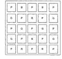
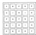
Fig. 6 A to Fig. 6 E is the plane graph according to the camera array of the isomery imager with different layouts of execution mode.
Fig. 7 be according to a kind of demonstration of execution mode the flow chart of process of the enhancing image that generates by the lower resolution image of being taken by a plurality of imagers.
Embodiment
The preferred embodiment of the present invention is described now by reference to the accompanying drawings, wherein similar Reference numeral indication similar elements or the approximate element of function.And, in the accompanying drawings, the accompanying drawing that the numeral of the leftmost side of each Reference numeral is used for the first time corresponding to this Reference numeral.
Execution mode relates to the use distributed method with the imager photographic images by a plurality of different imaging features of employing.Each imager can spatially depart from another imager as follows: the image that imager is taken is with respect to the amount of the image shift sub-pixel of another imager shooting.Each imager also can comprise the independently optical element with different filters and move with different operational factor (for example time for exposure).The picture rich in detail that processing is generated by described imager is to obtain the image of enhancing.Each imager can be with related by the optical element that uses wafer scale optics (WLO) fabrication techniques.
Sensor element or pixel refer to the independent light perception element in camera array.Described sensor element or pixel comprise traditional CIS (cmos image sensor), CCD (charge coupled device), high dynamic range pixel, multispectral pixel and various alternative elements and some other sensor element.
Imager refers to two-dimensional array.The sensor element of each imager has similar physical property and receives light by identical optical module.In addition, the sensor element in each imager can be associated with identical the color filter.
Camera array refers to the set of imager, and this set is designed to move as single component.Described camera array can make be used for assembling or be mounted to various device on one chip.
A series of camera array refer to the set of two or more camera array.But two or more camera array cooperations are to provide expanded function with respect to single camera array.
The characteristics of image of imager refers to any feature or the parameter relevant with image taking.Described characteristics of image can comprise inter alia: the kind of imager size, the contained pixel of imager, the shape of imager, to time for exposure of the related filter of imager, imager, the aperture scale relevant with imager, the layout with the related optical element of imager, the gain of imager, the resolution of imager, the operation sequential of imager.
The structure of camera array
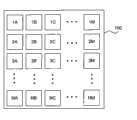
Fig. 1 hasimager 1A to the plane graph of thecamera array 100 of imager NM according to a kind of executionmode.Camera array 100 is made on semiconductor chip to comprise that a plurality ofimager 1A are to imagerNM.Imager 1A can comprise a plurality of pixels (for example 0.32 mega pixel) to each of imager NM.In one embodiment,imager 1A is arranged to the shown grid configuration of Fig. 1 to imager NM.In other execution mode, described imager is arranged as the form of non-grid.For example, described imager can be arranged as circular layout, zigzag layout or scattered distribution.
Described camera array can comprise two or more isomery imagers, and each imager comprises two or more sensor elements or pixel.In described imager, each can have different characteristics of image.Perhaps, two kinds of different or more kinds of different imagers can be arranged, wherein the total identical characteristics of image of the imager of identical type.
In one embodiment, each to the imager NM ofimager 1A has oneself filter and/or optical element (for example lens).Particularly,imager 1A can be associated to receive with the color filter of spectrum the light of specific wavelength to each or one group of imager of imager NM.The filter of example comprises traditional filter that uses, IR-cut filter, near-infrared filter, polarization filter and to satisfy the customization filter of Hyper spectral Imaging demand in bayer-pattern (R, G, B or their complementary C, M, Y).Some imagers can not have filter to receive the near infrared spectrum of whole visible spectrum and lifting imager signal to noise ratio.The number of clear filter can with camera array in the number as much of imager.In addition, the lens of the aperture of each or one group ofimager 1A to the imager NM by having different optical feature (for example focal length) or different size can receive light.
In one embodiment, described camera array comprises other interlock circuits.Described other interlock circuits can comprise circuit and other circuit of controlling imaging parameters and controlling the sensor senses physical parameter.Control circuit can be controlled the imaging parameters such as time for exposure, gain and black level shift.Described transducer can comprise that dark pixel is with the dark current under the estimation working temperature.Described dark current can be measured to be used for that dynamic compensation is carried out in any thermal creep that substrate may suffer.
In one embodiment, be used for controlling the circuit of imaging parameters can be independently or trigger in a synchronous manner each imager.The beginning of the time for exposure of various imagers in camera array (be similar to and open shutter) can overlapping mode be staggered, the scene of sampling continuously when making some imagers be exposed to light simultaneously like this.In traditional cameras, with the speed sampling scene of N exposure of per second, the time for exposure of each sampling is limited in 1/N second.Rely on a plurality of imagers, there is no this type of restriction for time for exposure of each sampling, because can move a plurality of imagers with staggered mode photographic images.
But each imager of independent operating.Personalizable is processed and each whole or most operation that independently imager is relevant.In one embodiment, the main setting of programming (master setting) configures the deviation (i.e. skew or gain) of this main setting to each imager.Described deviation can reflect the function such as high dynamic range, gain setting, the setting time of integration, digital processing setting or their combination.To concrete camera array, these deviations can be specialized under low level (for example gain deviation) or higher level (for example the ISO number is poor, and the difference of this ISO number then automatically is converted into gain delta, the time of integration or is otherwise specialized by environment/main control register (context/master control register)).By main value being set and to the deviation of this main value, can realize the abstract simpler programming mode that is beneficial to realize to many operations of the control of higher level.In one embodiment, the parameter of imager is at random to fix to be used for target application.In another embodiment, described parameter is configured to allow flexibility and the programmability of height.
In one embodiment, camera array is designed to the existing replacement device that is used in the camera image transducer in mobile phone and other mobile devices.Therefore, described camera array can be designed to the traditional imageing sensor with approximate equal resolution compatible physically, yet can surpass traditional imageing sensor in the resolution that the described camera array of many shooting occasions reaches.The advantage of the performance that utilize to promote, the camera array of this execution mode can have still less pixel than traditional imageing sensor and obtain equal or better quality image.Alternatively, when obtaining similar results, in described imager, the size of pixel can reduce than the pixel in conventional image sensor.
For the original image prime number of coupling conventional image sensor under the prerequisite that does not enlarge silicon area, independently the logic expense of imager preferably is limited in area of silicon wafer.In one embodiment, most pixel control logic is the single set of the common function of whole or most of imagers, and described imager has the less function collection that can be applicable to each imager.In this embodiment, because the output data of described imager significantly do not increase, so traditional external interface can be used for described imager.
In one embodiment, the conventional image sensor that has the camera array replacement M mega pixel of imager.Described camera array comprises N * N imager, and each transducer has M/N2Individual pixel.Each imager of camera array also has the depth-width ratio identical with the conventional image sensor that is replaced.Table 1 is listed the example arrangement according to the camera array of replacement conventional image sensor of the present invention.
Table 1

The super-resolution factor in table 1 draws for estimation, and based on the super-resolution factor by the resulting reality of processing, the effective resolution value can be different.
The number of the imager in camera array can be determined based on following factor: (i) resolution, (ii) parallax, (iii) photosensitivity, (iv) dynamic range and some other factor.First factor that affects described imager size is resolution.From the angle of resolution, the scope of the preferred number of described imager is 2 * 2 to 6 * 6, because probably destroy the frequency information that can not be rebuild by super-resolution processing method greater than 6 * 6 array scale.For example, 8 each imager of mega pixel resolution requirement that have 2 * 2 imagers have 2 mega pixels.Similarly, each imager of 800 ten thousand resolution requirement that has 5 * 5 arrays has 0.32 mega pixel.
The second factor that may limit the imager number is parallax and covers (occlusion) problem.About taking the object to the image, the background parts of the eye-patching of described imager is called as " covering collection ".When two imagers during from two different positions shot objects, each imager to cover collection different.Therefore, may have the scene pixel to be photographed by an imager, and another imager does not photograph this scene pixel.Cover problem in order to solve this, for the imager of given type, expectation comprises the imager of some minimal sets.
The 3rd factor that may restrict imager number lower limit is the photosensitivity problem under low light environment.In order to improve low light level photosensitivity, may need for the imager of surveying near infrared spectrum.The number of the imager in described camera array may need to increase to adapt to this near infrared imaging device.
The 4th factor that determines described imager number is dynamic range.For the dynamic range of camera array is provided, it is favourable that the imager of some identical filter kinds (colourity or brightness) is provided.Each in the imager of identical filter kind can be moved under different exposure then simultaneously.Can be processed to generate high dynamic range images by the image that the difference exposure is taken.
Based on these factors, the preferred number of imager is 2 * 2 to 6 * 6.4 * 4 and 5 * 5 layout is more more preferred than 2 * 2 and 3 * 3 layout, because the former more may provide the imager of enough numbers to cover problem, improve photosensitivity and improve dynamic range with solution.Meanwhile, restore the required computational load of resolution by these matrix numbers and want appropriateness than the required computational load of 6 * 6 arrays.Yet the array greater than 6 * 6 can be used for providing the supplementary features such as optical zoom and multispectral imaging.
Another factor that need to consider is the imager number for the brightness sampling.By guaranteeing that the imager that is used for the near-infrared sampling in array does not reduce the resolution that reaches, the information of near-infrared image adds by the taken resolution of brightness imager.For this reason, at least 50% imager can be used for taking a sample brightness and/or near infrared spectrum.In an execution mode with 4 * 4 imagers, 4 imagers sampling brightness, 4 imagers sampling near infrared spectrums remains two colourities of 8 imagers samplings (red and blueness).Have in the execution mode of 5 * 5 imagers 9 imager sampling brightness, 8 imager sampling near infrared spectrums, two kinds of colourities of remaining 8 imagers sampling (red and blue) at another.In addition, the imager that has these filters is symmetrical arranged to tackle by covering that parallax causes in camera array internal medicine.
In one embodiment, the imager in camera array is spatially spaced apart a predetermined distance.By increasing the spatial separation distance, can increase the parallax between the image that described imager photographs.When more accurate range information became important, the parallax of increase was favourable.Also can increase by 2 intervals between imager to simulate the interval between a pair of human eye.By simulation people interorbital space, can provide three-dimensional 3D rendering true to nature that the gained image is presented on suitable 3D display device.
In one embodiment, the diverse location at equipment arranges the polyphaser array to overcome spatial limitation.A camera array can be designed to be arranged in restricted clearance, and another camera array can be placed in another restricted clearance of described equipment.For example, if altogether need 20 imagers, it is 1 * 10 camera array that but free space only allows the either side at equipment that imager is set, and two camera array can be positioned over the free space of described equipment both sides so, and each comprises 10 imagers described two camera array.Mainboard or other parts of equipment can be made and be fixed to each camera array in substrate.Image by a plurality of camera array collections can the processed image that has desired resolution and performance with generation.
The design of single-imager can be applicable to different camera array, and each camera array has the imager of other kinds.Its dependent variable in camera array is adjustable to produce the camera array with different imaging features, described variable such as space length, the color filter and with the combination of identical transducer or other transducers.By this way, when the scale of keeping is saved, can produce the camera array of multiple mixing.
Wafer scale optics is integrated
In one embodiment, camera array adopts wafer scale optics (WLO) technology.The WLO technology is that optics is molded on chip glass, and then optics is direct and imager is encapsulated into single chip integrated module.The WLO operation can comprise uses the diamond turning mould to make each plastic lens elements and some other operation on substrate of glass.
Fig. 2 A is the stereogram according to a kind ofcamera array assembly 200 withwafer level optics 210 andcamera array 230 of execution mode.Wafer level optics 210 comprises a plurality oflens elements 220, and eachlens element 220 covers one of 25imagers 240 in camera array 230.Notice thatcamera array assembly 200 has less lens element row, these lens element row are compared the single large lens that coverwhole camera array 230 and will be occupied much smaller space.
Fig. 2 B is the cutaway view according to a kind of camera array assembly 250 of execution mode.Camera array 250 comprises top lens wafers 262, bottom lens wafer 268, substrate 278 and spacer block 258, spacer block 264 and spacer block 270, and a plurality of imagers are formed on described substrate 278.Camera array assembly 250 is packaged in packaging part 254.Top spacer block 258 is placed between packaging part 254 and top lens wafers 262.A plurality of optical elements 288 are formed on top lens wafers 262.Middle ware spacer block 264 is placed between top lens wafers 262 and bottom lens wafer 268.Another group optical element 286 is formed on bottom lens wafer 268.Bottom interval piece 270 is placed between bottom lens wafer 268 and substrate 278.Also be provided with silicon clear opening 274 with the path of the signal that is provided for transmitting described imager.Top lens wafers 262 can partly be coated with resistance luminescent material (for example chromium) 284 to intercept light.The part of the uncoated resistance luminescent material 284 of top lens wafers 262 plays a part aperture, and light exposes to bottom lens wafer 268 and described imager by this aperture.In the execution mode of Fig. 2 B, filter 282 is formed on bottom lens 268.Resistance luminescent material 268 (for example chromium) also can be coated on the effect that optical isolator is played in bottom lens 268 and substrate 278.The lower surface of described substrate is coated with back redistributing layer (" RDL ") and soldered ball 276.
In one embodiment,camera array assembly 250 has 5 * 5 imager array.The width W ofcamera array 250 is 7.2mm, and length is 8.6mm.The width S of each imager in camera array can be 1.4mm.The total height t1 of optics is approximately 1.26mm, and the total height t2 of camera array assembly is lower than 2mm.
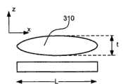
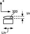
Fig. 3 A and Fig. 3 B are the figure that has shown that the lens element height changes with the change in size on x-y plane.The size of thelens element 320 in Fig. 3 B only has the 1/n oflens element 310 in Fig. 3 A.Because the diameter L/n oflens element 320 is the 1/n oflens element 310 diameter L, the height t/n oflens element 320 is similarly the 1/n oflens element 310 height t.Therefore, by using the array of less lens element, the height of camera array can obviously reduce.The height of the reduction of camera array assembly can be in order to the more cheap lens of design, and described lens have better optical property, improve such as main perspective improvement, distortion reduction and aberration.
Fig. 3 C has shown that the thickness by reducing the camera array assembly improves main perspective (CRA).CRA1 is signal-lens main perspective, and this einzel lens covers whole camera array.Although can reduce main perspective by the distance that increases between camera array and lens, the thickness constraint has restricted the increase of described distance.Therefore, the CRA1 of camera array with single lens element is large, causes reducing optical property.CRA2 is the main perspective of the imager in camera array, and the thickness of this camera array and other sizes are adjusted.It is identical with the CRA1 of traditional camera array that CRA2 keeps, and therefore do not improve on main perspective.Yet as shown in Figure 3, by changing the distance between described imager and lens element, the main perspective CRA3 of camera array assembly can be minimized than CRA1 or CRA2, thereby obtains better optical property.As mentioned above, camera array according to the present invention has the thickness demand of reduction, and therefore, the distance of lens element and camera array can increase to improve main perspective.
In addition, than the conventional lenses element of covering wide spectrum, the impact that described lens element is subjected to strict design constraint still less, but produce performance better or that be equal to because each lens element can be designed to guide the light of narrow bandwidth.For example, the imager of reception visible spectrum or near infrared spectrum can have the lens element of special optimization to be used for this band.For the imager of surveying other spectrum, lens element can have different focal lengths, and the focal plane of the different bands of light is identical like this.The coupling focal plane has increased the acutance of the image that described imager photographs and has reduced longitudinal chromatic aberration in the different wavelength range of light.
Other advantages than the lenslet element comprise that cost, material usage reduce, production process reduces and some other advantage.By n is provided2Individual on x direction and y direction the lens of 1/n size (so thickness is 1/n), also can be minimized for the production of the wafer size of lens element.This has significantly reduced cost and the consumption of material.In addition, the quantity of lens substrate is also reduced, and causes the process number to reduce and the thereupon reduction of production cost.Described lens arra pairing is usually stricter unlike the situation of traditional imager to the required placement accuracy of described imager, because substantially identical with traditional imageing sensor according to the Pixel Dimensions of camera array of the present invention.
In one embodiment, WLO manufacturing process comprises: (i) before lens are moulded, add lens stop on substrate by lens stop is covered; And (ii) etched hole and the lens by described substrate are carried out double-faced forming in described substrate.Etch-hole is favourable in described substrate, because can not cause the index mismatch between plastics and substrate.By this way, can use the light absorption substrate of the natural diaphragm (being similar to the blacking rims of the lens) that forms all lens elements.
In one embodiment, filter is the part of imager.In another embodiment, filter is the part of WLO subsystem.
Imaging system and processing streamline
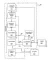
Fig. 4 shows is functional block diagram according to theimaging system 400 of one embodiment of the presentinvention.Imaging system 400 can comprisecamera array 410, imageprocessing pipeline module 420, controller 440 and some otherparts.Camera array 410 comprises above two or more by reference to the accompanyingdrawings 1 and the imager described in detail of accompanying drawing 2.Image 412 is captured by two or more imagers incamera array 410.
Controller 440 is hardware, software, firmware or their combinations for the various operational factors of controlling camera array 410.Controller 440 receivesinput signal 446 and operation signal 442 to controlcamera array 410 from user or other external modules.Controller 440 can also sendinformation 444 to image andprocess pipeline module 420 with the processing ofassistant images 412.
Imageprocessing pipeline module 420 is hardware, firmware, software or their combinations for the treatment of the image that receives from camera array 410.Following 5 described in detail by reference to the accompanying drawings, image is processedpipeline module 420 and is processed a plurality of images 412.Then image 422 after processing sends be used for demonstration, storage, transmission or further process.
What Fig. 5 showed is to process the functional block diagram ofpipeline module 420 according to a kind of image of execution mode.Image is processedpipeline module 420 can comprise upstreamtrack process modules 510, image pixel relating module 514, parallax confirmation andmeasurement module 518,parallax compensation module 522,super-resolution module 526,address conversion module 530, address and phasedeviation calibration module 554, downstreamcolor treatments module 564 and some other assembly.
Address and phasedeviation calibration module 554 are the storage facilitiess for the stored calibration data, and described calibration data is to generate during the camera array in manufacturing process or follow-up calibration process again characterizes.Calibration data is presented at the address ofphysical picture element 572 of imager and thelogical address 546 of image, the mapping betweenlogical address 548.
Upstreamtrack process modules 510 provides theimage 412 of being taken by image processor 540.Upstreamtrack process modules 510 can be carried out that black level calculates and adjust, and steady noise compensation, optical point spread function (PSF) deconvolute, one or more in reducing noise and clutter reduction.After upstreamtrack process modules 510 was processed described image, image pixel relating module 514 was carried out and is calculated to solve parallax, and described parallax is along with subject becomes more obvious near described camera array.Particularly, image pixel relating module 514 will mate that described parallax is compensated by the image section that different imagers are taken.In one embodiment, image pixel relating module 514 compares the difference between the average of neighbor and threshold value, and when described difference surpassed described threshold value, the mark parallax may exist.Described threshold value changes with the operation conditions capable of dynamic of described camera array.In addition, also adaptive and can reflect the concrete operation conditions of selected imager in abutting connection with calculating.
Process described images to survey and to measure described parallax by parallax confirmation and measurement module 518 subsequently.In one embodiment, realize the parallax detection by the pixel Correlation monitoring device of operation.This operates in the logical pixel space of whole imagers and carries out with the similar condition time of integration.When scene reality at infinity, the data height correlation of described imager also only is subjected to impact based on the variation of noise.Yet when object close enough camera, the parallax effect that changes correlation between imager is introduced into.Due to the space layout of imager, the character of the change that parallax causes is consistent in all imager scopes.Be subjected in the scope of restriction of certainty of measurement, the relevant difference domination between any a pair of imager is another poor in the difference between imager and other imager scopes arbitrarily.By other are carried out same or similar calculating to imager, this redundancy of information makes the high accuracy parallax confirm and measure and can realize.If there is parallax in other to imager, consider the position of described imager, described parallax should roughly appear at the identical physical location of described scene.Track by keeping various paired measurements and calculate " reality " differential parallax in the mode of least square method (or similar statistical method) match sampled data can be realized parallax measurement simultaneously.Can comprise for the additive method of surveying described parallax the high frequency imaging element of surveying frame by frame and follow the trail of vertical direction and horizontal direction.
After the parallax of accurately having determined concrete imager changed,parallax information 524 was sent to address conversion module 530.Address conversion module 530use parallax informations 524 and from thecalibration data 558 of address and phasedeviation calibration module 554 so that determine will be for suitable X side-play amount and the Y side-play amount of logical pixel address computation.Address conversion module 530 determines that also concrete imager pixel is with respect to the associated sub-pixels skew of the pixel in the result images 428 that is generated by SUPERRESOLUTION PROCESSING FOR ACOUSTIC.Address conversion module 530 is consideredparallax information 524 and is providedlogical address 546 to solve this parallax.
As following being described in detail, after carrying out parallax compensation, described image is processed to obtain by the synthetic high-definition picture 422 of low-resolution image by super-resolution module 526.Synthetic image 422 can provide to downstreamcolor treatments module 564 subsequently to carry out one or more in following operation: focus on recovery, white balance, chromatic aberration correction, gamma correction, RGB to YUV corrections, edge sensitive sharpening, contrast strengthens and compress.
Image is processedpipeline module 420 and can be comprised for image being carried out the assembly of other processing.For example, image processing flowingwater module 420 can comprise the abnormal correction module that is caused by single picture element flaw or picture element flaw group for proofreading and correct.Correction module can be contained on the same chip at described camera array place, can be used as the assembly that separates with described camera array or as the part ofsuper-resolution module 526.
SUPERRESOLUTION PROCESSING FOR ACOUSTIC
In one embodiment,super-resolution module 526 is by processing the low-resolution image that photographed byimager 540 to generate more high-resolution composograph.The overview image quality of composograph will be higher than the image by in imager, any photographs separately.In other words, each imager cooperating operation, each imager utilize ability separately in the situation that need not the narrow section that sub sampling is taken spectrum, thereby all make contributions for higher-quality image.The image relevant to super-resolution technique forms can be expressed as following formula:
yk=Wk·x+nk,
W whereinkRepresent the LR image (y of HR scene (x) (by obfuscation, action and sub sampling) to being photographed by k imagerk) contribution, nkIt is noise contribution.
Fig. 6 A to Fig. 6 E has shown the various layouts that are used for obtaining by SUPERRESOLUTION PROCESSING FOR ACOUSTIC the imager of high-definition picture according to one embodiment of the present invention.In Fig. 6 A to Fig. 6 E, " R " representative has the imager of red filter, and " G " representative has the imager of green filter.The imager that " B " representative has blue filter, " P " representative has photosensitive polychrome imager in whole visible light and near infrared spectral range, and " I " representative has the imager of near-infrared filter.Described polychrome imager can be from whole sampled images of visible light and near infrared region (also namely from 650nm to 800nm).In the execution mode of Fig. 6 A, the imager of middle columns and rows has the polychrome imager.The remaining area of camera array is furnished with imager with green filter, have the imager of blue filter and have the imager of red filter.The execution mode of Fig. 6 A does not comprise any imager of independent detection near infrared spectrum.
The execution mode of Fig. 6 B has the layout that is similar to traditional Bayer filter distribution.This execution mode does not comprise any polychrome imager or near infrared imaging device.As above 1 ground described in detail by reference to the accompanying drawings, the execution mode of Fig. 6 B is different from traditional Bayer filter layout, is matched to single pixel because each the color filter is matched to each imager.
Fig. 6 C has shown that a kind of polychrome imager forms the execution mode of symmetrical chessboard pattern.Fig. 6 D has shown the execution mode with 4 near infrared imaging devices.Fig. 6 E has shown the execution mode with irregular coupling imager.Fig. 6 A to Fig. 6 E is only illustrative nature, also can use the imager of other various layouts.
It is favourable using polychrome imager and near infrared imaging device, because these transducers can be taken high quality graphic according under environment at the low light level.The image that is photographed by polychrome imager or near infrared imaging device is used for removing the noise of the image that is obtained by the general color imager.
By assembling prerequisite that a plurality of low-resolution images increase resolution based on the following fact: different low-resolution images has represented the slightly different visual angle of same scene.If the LR image is the integer unit of mobile pixel all, so every width image comprises identical information basically.Therefore, do not have fresh information can be used for generating the HR image on the LR image.In the imager of foundation execution mode, the layout of described imager is predeterminable and controlled, and such row or each imager of delegation are adjacent has the stator pixel distance between imager.Wafer-level fabrication and encapsulation process allow the Accurate Shaping of imager to reach the required subpixel accuracy of SUPERRESOLUTION PROCESSING FOR ACOUSTIC.
The problem that the spectrum induction element is divided into different imagers is the parallax that the physical separation by described imager causes.Place by guaranteeing that described imager is symmetrical, at least two imagers can be taken near the pixel in foreground object edge.By this way, near the pixel described foreground object edge can assemble to increase definition and avoid any and covers.The sampling that another problem relevant to parallax is color.The problem of color sampling can reduce by using the parallax information in the polychrome imager, thereby improves the accuracy of the color sampling of being undertaken by the color filter imager.
In one embodiment, the near infrared imaging device is poor with respect to the relative brightness of visible light for determining.Object has the different materials reflectivity and causes visible light and near infrared spectrum to photograph the difference of image.Under low light environment, described near infrared imaging device shows higher signal to noise ratio.Therefore, the signal of near infrared sensor can be used for the image that highlights.Before the spectrum picture of assembling different imagers carried out SUPERRESOLUTION PROCESSING FOR ACOUSTIC, details from near-infrared image to luminance picture that can carry out from transformed.By this way, the marginal information of scene can be improved builds the image that the edge keeps, and can effectively utilize this image in SUPERRESOLUTION PROCESSING FOR ACOUSTIC.Use the advantage of near infrared imaging device apparent according to formula (2), wherein any improvement in noise (being also n) estimation causes the better estimation of original HR scene (x).
Fig. 7 has shown that the LR image of being taken by a plurality of imagers according to a kind of basis of execution mode generates the process chart of HR image.At first, the imager in camera array is taken luminance picture, near-infrared image and color image (step 710).Then the image that photographs is carried out regularization and arrive with the physical address map with described imager the logical address (step 714) that strengthens image.Then carry out parallax compensation to solve any difference (step 720) in the imager visual field that is caused by described imager spatial separation.Then carry out SUPERRESOLUTION PROCESSING FOR ACOUSTIC to obtain super-resolution luminance picture, super-resolution near-infrared image and super-resolution chromatic diagram picture (step 724).
Then determine whether light status is better than parameter preset (step 728).If light status is better than described parameter, process enters into respect to super-resolution luminance picture standardization super-resolution near-infrared image (step 730) so.Then carry out to focus on and recover (step 742).In one embodiment, use PSF (some diffusion function) that each passage deblurring is carried out to focus on and recover (step 742).Then, process super-resolution (step 746) based on near-infrared image and luminance picture.Then, composograph is built (step 750).
If determine light status unlike parameter preset good (step 728), mate super-resolution near-infrared image and luminance picture (step 734).Then, use the near-infrared super resolution image to carry out noise reduction (step 738) to the super-resolution luminance picture.Then, flow process enters into to carry out to focus on recovers (step 742), and carries out the identical flow process that is better than parameter preset when light status.Then, flow process finishes.
The image co-registration of color image and near-infrared image
The spectral response of cmos imager is usually very good at the near infrared region of containing 650nm to 800nm, and fairly good between 800nm to 1000nm.Although near-infrared image does not have chrominance information, the information of this SPECTRAL REGION is useful in low light environment, because described near-infrared image does not have noise comparatively speaking.Therefore, near-infrared image can be used for removing the picture noise under low light environment.
In one embodiment, from the image of near infrared imaging device and another width image co-registration from the visual light imaging device.Before merging, carry out registration (registration) to solve visual field difference problem between near-infrared image and visible images.Can carry out register flow path in off-line, disposable treatment step.After having carried out registration, be inserted in the monochrome information on near-infrared image in the lattice point corresponding to each lattice point on visible images.
After the pixel correspondence of having set up between near-infrared image and visible images, can carry out denoising and details transfer flow.The denoising flow process allows signal message be transferred to visible images to improve total signal to noise ratio of fused images from near-infrared image.Details transforms the edge of guaranteeing near-infrared image and visible images and is kept and give prominence to improve the overall observability of object in fused images.
In one embodiment, the near-infrared flash of light can be used as by the near-infrared light source during near infrared imaging device photographic images.Use the near-infrared flash of light to have superiority, except other reasons, because (i) can avoid interest object illumination high light; (ii) can preserve the environmental colors of object; And (iii) can avoid red-eye effect.
In one embodiment, use and only to allow visible light filter that near infrared light passes through with the optical effect of further optimization near infrared imaging.The visible light filter improves the near-infrared optical transformation function, because the visible light filter causes details sharper keen in near-infrared image.Then use dual bilateral filter details can be transferred to visible images, described dual bilateral filter such as Eric P.Bennett et ai., " MultispectralVideo Fusion; " Computer Graphics (ACM SIGGRAPH Proceedings) (July25,2006) described, the document is incorporated this paper into by reference at this in full.
Determine dynamic range according to the difference exposure of imager
Automatic exposure (AE) algorithm is important for the proper exposure of obtaining scene to be taken.The design of AE algorithm affects the dynamic range of photographic images.Described AE algorithm determines to allow the image that obtains fall into the exposure value of the range of linearity of camera array sensitive volume.This range of linearity is preferred, because the signal to noise ratio that can obtain in this zone.If it is too low to expose, the image desaturation that can become, and if expose too high, the supersaturation that becomes of described image.In traditional camera, adopt the image brightness that iterative processing measures with reduction and preset difference between brightness with lower than threshold value.This iterative processing needs the plenty of time to be used for convergence, and sometimes causes unacceptable shutter delay.
In one embodiment, the image brightness by the captured image of a plurality of imagers is independent measurement.Particularly, thus a plurality of imagers are set to be reduced with different exposure photographic images and calculates the fully time of exposure.For example, in the camera array with 5 * 5 imagers, have 8 brightness imagers and 9 near infrared imaging devices, each imager can be set up has different exposure values.The near infrared imaging device is used for taking the low light level face of scene, and the brightness imager is used for taking the high brightness face of described scene.This has caused ading up to 17 may expose.For example, if the exposure of each imager departs from abutting connection with 2 values of imager, the maximum dynamic range that can photograph so is 217Or 102dB.On the quite large degree of the dynamic range of this maximum higher than the value of the obtainable 48dB of being generally in the traditional camera with 8 outputs.
Instantaneous at each, based on needing how many kinds of exposure in follow-up time, analyzes in a plurality of imagers the response (under-exposed, overexposure or optimize and expose) of each.Than once testing a kind of situation of exposure, inquire about simultaneously the ability of multiple exposure and accelerated search in the scope that may expose.Determine the fully processing time of exposure by reducing, can reduce shutter delay and continuous shooting sluggish.
In one embodiment, by changing into the picture device in linearity to fused images after the response of each exposure, the HDR image forms by multiexposure, multiple exposure is synthetic.The image of described imager can register to solve the visual field difference problem of described imager before merging.
In one embodiment, at least one imager has the HDR pixel to generate the HDR image.The HDR image is the special pixel of taking the high dynamic range scene.Although the HDR pixel demonstrates more excellent performance with respect to other pixels, the performance that the HDR pixel is gone on business than the performance of near infrared imaging device under low light environment.In order to improve the performance under low light environment, the signal of HDR imager can use to obtain the more image of good quality under the different light rays environment with the signal of near infrared imaging device is collaborative.
In one embodiment, by processing the image acquisition HDR image of being taken by a plurality of imagers, described processing for example hereinafter discloses: Paul Debevec et aI., " Recovering High DynamicRange Radiance Maps from Photographs; " Computer Graphics (ACM SIGGRAPHProceedings), (August 16,1997), the document is incorporated this paper into by reference at this in full.The ability of using imager to take simultaneously a plurality of exposures has superiority, because the pseudo-shadow that is caused by object of which movement in scene can be alleviated or eliminate.
The high light spectrum image-forming of a plurality of imagers
In one embodiment, play up multispectral image to promote object segmentation or identification in scene by a plurality of imagers.Due to spectral reflectance factor smooth change on the object of most real worlds, the imager that has the different colours filter by use is taken the scene of multispectral scope and is used main component analysis (Principal Components Analysis, PCA) analyze captured image, can estimate described spectral reflectance factor.
In one embodiment, in camera array, the imager of half is used for sampling in basic spectral region (R, G and B), second half imager be used for the basic spectral region of displacement (R ', 0 ' and B ') sample.The basic spectral region of displacement is to move certain wavelength (for example 10nm) from basic spectral region.
In one embodiment, carry out pixel correspondence and non-linear interpolation to solve the sub-pixel visual angle displacement problem of scene.Then, use the spectral reflectance factor of the synthetic scene of one group of quadrature spectrum basic function, described basic function for example hereinafter discloses: J.P.S.Parkkinen, J.Hallikainen and T.Jaaskelainen, " Characteristic Spectra of Munsell Colors; " J.Opt.Soc.Am., A 6:318 (August1989), this article is incorporated this paper into by reference at this in full.Described basic function is the characteristic vector that the PCA by coefficient matrix derives, and described coefficient matrix is to be derived out by the database of storage spectral reflectance factor, described spectral reflectance factor is measured (for example) to rebuild the spectrum of every bit in described scene by Meng Saier color lump (ading up to 1257), and described Meng Saier color lump has represented the large-scale spectral distribution of real world material.
Under just looking, the different spectrum pictures of taking scenes by the different imagers of camera array are seemingly sacrificed resolution and are obtained wider spectrum sample.Yet the resolution of some losses can be recovered.Many imagers are sampled to the different spectral regions of described scene, and wherein each sampling lattice point of each imager is offset a sub-pixel each other, and in one embodiment, this imager does not have two sampling lattice points overlapping.In other words, the stack of all sampling lattice points of all imagers form fine and close, may be the splicing of point heterogeneous.Can use the separate data interpolating method with the spectral concentration of each sampled point in this non-homogeneous spliced map of determining each spectrum picture, for example with described in Publication about Document, ShiaofenFang et aI., " Volume Morphing Methods for Landmark Based 3D ImageDeformation " by SPIE vol.2710, proc.1996 SPIE Inti Symposium on MedicalImaging, page 404-415, Newport Beach, CA (February 1996), the document is incorporated this paper into by reference at this in full.By this way, in the process of using different spectrum filter sampled images, a certain amount of resolution loss can be resumed.
As mentioned above, be conducive to image segmentation and object identification by the spectral reflectance factor of determining object.This situation often comes across safety applications, uses camera network to follow the trail of this object when wherein moving to the Operational Zone of another camera from the Operational Zone of a camera when object.Each zone has the light environment (fluorescent light thread environment, incandescent light thread environment, D65 light environment etc.) of himself uniqueness, and this light environment can cause object to have different outward appearances in each image of being taken by different cameral.If these cameras are taken under high spectral patterns, all images can be converted into same light source to strengthen the object recognition performance.
In one embodiment, use has the camera array of a plurality of imagers so that medical diagnostic image to be provided.The full spectrum digitized image of diagnostic sample helps Precise Diagnosis, because doctor and medical worker have higher confidence for diagnostic result.Imager in camera array can have the color filter so that full spectroscopic data to be provided.In these camera array, imager can be mounted to mobile phone to take and to transmit diagnostic message position afield, for example hereinafter described, Andres W.Martinez et ai., " Simple Telemedicine forDeveloping Regions:Camera Phones and Paper-Based Microfluidic Devices forReal-Time; Off-Site Diagnosis; " (April 11 for Analytical Chemistry (American ChemicalSociety), 2008), this article is incorporated this paper into by reference at this in full.In addition, the camera array that has a plurality of imagers can provide the reliability of image with the large depth of field IMAQ to strengthen wound, measles and other symptoms.
In one embodiment, use the little imager (for example having the 20-500 pixel) with the logical filter of narrow band to generate the feature of environment and local light source in scene.By using little imager, exposure and white balance feature can be determined quickly and more accurately.The logical filter of described band can be common the color filter or bandpass width diffraction element, and this bandpass width diffraction element is enough to allow the camera array number contain the approximately visible light of 400nm.These imagers can be with the fast data (these data may or may not be used in picture material) of moving and obtaining for the treatment of the information of the exposure that generates other larger imagers in the identical camera array of control and white balance of higher frame.Described little imager also may be interspersed within described camera array.
The optical zoom that uses many imagers to carry out
In one embodiment, the subset of the imager in camera array comprises long focus lens.The subset of imager can have other imaging features identical with other non-long focus lens imagers.Image from this subset of imager is merged with SUPERRESOLUTION PROCESSING FOR ACOUSTIC to form the long burnt image of super-resolution.In other execution mode, camera array has two or more imager subsets, and described imager has the lens that amplify higher than twice to provide different zooms to amplify.
The execution mode of camera array can be realized final resolution by the image of assembling SUPERRESOLUTION PROCESSING FOR ACOUSTIC.5 * 5 imagers that for example have 3 Zoom Lens features, if 17 imagers are used for sampling brightness (G), 8 imagers are used for sampling colourity (R and B), and the resolution that 17 brightness imagers can be realized is higher than 4 times of the achieved resolution of any single imager in 17 imager groups.If described imager extends to 6 * 6 from 5 * 5, there are 11 extra imagers to use.Conventional image sensor than 8 mega pixels that 3 times of zoom lens are installed, 8 in 11 extra imagers in 3 times of zoom situations are used for sampling brightness (G), when remaining 3 imagers for sampling colourity (R and B) and near-infrared sampling, can realize the resolution of 60% conventional image sensor.This has reduced the ratio of chroma sampling (or near-infrared sampling) with the brightness sampling to a considerable extent.Super-resolution luminance picture by using 3 times of zoom places as to the identification basis of colourity (and near-infrared) image so that more high-resolution chromatic diagram picture is taken a sample again, compensated to a certain extent the reduction of colourity to the brightness sampling rate.
In the situation with 6 * 6 imagers, obtain the resolution that equates with conventional image sensor resolution under 1 times of zoom.At 3 times of zoom places, the obtainable resolution of identical imager is equal to 60% of conventional image sensor that 3 times of zoom lens are housed.In addition, than the resolution that conventional image sensor has under 3 times of zooms, the brightness resolution of described imager under 3 times of zooms decreases.Yet the brightness resolution of reduction is compensated by the following fact: the optical element of conventional image sensor has the efficient of reduction because crosstalking with optical aberration under 3 times of zooms.
The zoom operation of being realized by a plurality of imagers has following advantages.At first, realize the zoom quality that the quite large degree of quality of zoom realizes higher than conventional image sensor, because lens element can adapt to each variation of focal length.In traditional imageing sensor, optical aberration and the curvature of field must be proofreaied and correct in the whole opereating specification of lens, such correction in having the zoom lens of moving meter than much more difficult in the fixing lens element that only aberration of fixed focal length need be corrected.In addition, the fixed lens in imager has fixing main perspective for assigned altitute, and this situation from the conventional image sensor with mobile zoom lens is different.Secondly, described imager allows the simulation of zoom lens and need not to significantly improve the optical track height.Highly reducing allows thin assembly (even having the camera array of zoom capabilities) be achieved.
List in table 2 according to the required expense of certain other optical zoom of level in the support camera array of some execution modes.
Table 2

In one embodiment, the pixel mapping in image is to output image, and its size and resolution is corresponding to the zoom amount of expectation, to provide from wide-angle visual angle to the level and smooth zoom capabilities at maximum amplification times yield visual angle.Suppose that the lens than high magnification have the visual angle center identical with the lens of low enlargement ratio, available image information is that the image zone line has higher resolution than outer peripheral areas and can use.In the situation of 3 times or more unique enlargement ratios, the nested region of different resolution can have the resolution that increases towards the center.
Having resolution that the image that greatly enhances burnt effect most has is determined by the super-resolution ability of the imager that is equipped with long focus lens.Image with the widest visual field can be one of at least formatted with following dual mode.The first, wide view field image can be formatted as the image with unified resolution, and the hyperresolution of the imager group of the lens of wide angle determines wherein said resolution by being equipped with more.The second, wide field-of-view image is formatted as more high-definition picture, and the resolution of the core of this image is determined by the super-resolution ability of the imager group that is equipped with long focus lens.In low resolution zone, the information of pixel that every image-region reduces number level and smooth interpolation in " numeral " pixel coverage of big figure more.In such image, Pixel Information can processed and interpolation, becomes level and smooth from higher to the transformation in low resolution zone more like this.
In one embodiment, realize as follows zoom: by causing barrel distortion to some (or all) array lenses, the pixel of unbalanced like this number is used for the mid portion of every width image.In this embodiment, every width image all must be processed to remove tubbiness deformation.In order to produce wide angle picture, by the over-extraction sample, more lean on paracentral pixel by double sampling with respect to peripheral pixel.Along with the carrying out of zoom, the pixel of described imager periphery is rejected gradually, and the sampling of the pixel at more close described imager center increases.
In one embodiment, build texture filter (mipmap filter) allowing image be played up with the zoom ratio, this zoom amplitude is positioned at the concrete zooming range (for example 1 of camera array times of zoom amplitude and 3 is by the zoom amplitude) of optical element.Texture (Mipmap) is the precalculated optimized image group with benchmark image.Can create and 3 times of image sets that the zoom luminance picture is relevant by be down to 1 times from the benchmark ratio of 3 times.Every width image in this group is all a version of 3 times of zoom images of benchmark, reduces on rank but be in details.Use the texture rendering image to realize by the following method in the zoom rank of expectation: (i) photographic images under 1 times of zoom, the then coverage of other scene of zoom level of calculation expectation (be also in benchmark image which pixel need to play up to generate output image with the ratio that requires); (ii) for each pixel in covering collection, determine that this pixel is whether in the image that is covered by 3 times of zoom luminance pictures; (iii) if this pixel is available in 3 times of zoom luminance pictures, select so described two the corresponding pixels of texture image of two immediate texture images and interpolation (use smoothing filter) to generate output image; And if (iv) this pixel is unavailable in 3 times of zoom luminance pictures, the pixel of 1 times of luminance picture of selection reference and expanding to desired ratio to generate output pixel so.By using texture, any point between two given discrete levels (being also 1 times of zoom and 3 times of zooms) can be simulated level and smooth optical zoom.
The capture video image
In one embodiment, camera array generates high frame image sequence.But the imager isolated operation in described camera array is with photographic images.Than conventional image sensor, described camera array can be with N frame speed photographic images doubly, and wherein N is the number of described imager.In addition, the frame period of each imager can be overlapping to improve the operation under low light environment.In order to increase resolution, the subset of imager can move to generate high-definition picture in a synchronous manner.In this case, largest frames speed reduces with the multiple of the imager number of method of synchronization operation.The high-speed video frame rate can allow the slow motion video with the playback of ordinary video speed.
In one embodiment, use two brightness imagers (green imager or near infrared imaging device), two blue imagers and two green imagers to obtain high definition 1080p image.Use the arrangement of four brightness imagers (two green imagers and two near infrared imaging devices or three green imagers and a near infrared imaging device), a blue imager and a red imager, for the 1080p video, but the described colourity imager of raising frequency sampling is to realize for 120 frame/seconds.As equipment, the number of frame speed can increase with linear scale for higher frame short-term training.For SD (480p) operation, use identical camera array can realize the frame speed of 240 frame/seconds.
Traditional imaging device with high-resolution image sensors (for example 8 mega pixels) uses compound or jumps and sample to take the more image of low resolution (for example 1080p30,720p30 and 480p30).In recombination process, insert electric charge, voltage or pixel domain in the row and column of captured image to fall the low noise target video resolution of obtaining simultaneously.In the sampling of jumping, the row and column sampling instrument that jumped reduces the transducer energy consumption.Two kinds of technology all cause picture quality to reduce.
In one embodiment, the imager in camera array is selectively activated with the capture video image.For example, can use 9 imagers (comprising 1 near infrared imaging device) to obtain 1080p (1920 * 1080 pixel), can use 6 imagers (comprising 1 near infrared imaging device) to obtain 720p (1280 * 720 pixel) image, perhaps can use 4 imagers (comprising 1 near infrared imaging device) to obtain 480p (720 * 480 pixel) image.Due to accurate point-to-point pixel corresponding relation being arranged between imager and target video image, the resolution that the resolution that obtains will obtain higher than traditional approach.In addition, because described imager only has a subset to be activated with photographic images, so also can realize significant energy consumption saving.For example, can reduce by 60% energy consumption in 1080p, and can reduce by 80% energy consumption in 480p.
It is favourable using near infrared imaging device capture video image, because can utilize the information of described near infrared imaging device to remove the noise of each video image.By this way, the camera array of execution mode shows good low light level photonasty and can move under extremely weak light environment.In one embodiment, the image that a plurality of imagers is obtained carries out SUPERRESOLUTION PROCESSING FOR ACOUSTIC to obtain more high-resolution video image.The noise reduction performance of SUPERRESOLUTION PROCESSING FOR ACOUSTIC makes image have low-down noise together with the image co-registration of described near infrared imaging device.
In one embodiment, realize high dynamic range (HDR) video capture by activating more imagers.For example, move 5 * 5 camera array under the 1080p video shooting mode, only have 9 cameras to activate.Can make the subset overexposure of 16 cameras and under-exposure by 2 or 4 one group of modes once, thereby realize having the very video output of high dynamic range.
Other application of many imagers
In one embodiment, use a plurality of imagers with the distance of estimation object in the scene.Because the information about the distance of each point in image can be utilized in camera array together with the x coordinate of pictorial element and the size of y coordinate, therefore can determine the size of pictorial element.In addition, the absolute dimension of actual object and shape can be measured and be need not other reference informations.For example, can take the picture of pin, resulting Information Availability is in the size of accurately estimating suitable shoes.
In one embodiment, the service range information simulation is by the reduction of the depth of field in the image of camera array shooting.Generate according to camera array of the present invention and have the image that the depth of field increases greatly.Yet, do not expect in some applications the long depth of field.In this case, can choose a specific range or some distances as " optimum focusing " distance of image, and based on the range information that gets from parallax information, use the method such as Gaussian Blur can pursue the fuzzy described image in pixel ground.In one embodiment, utilize the depth map obtained by camera array to activate tone-mapping algorithm, carrying out mapping with depth of view information with management level, thereby emphasize or strengthen 3D effect.
In one embodiment, provide the aperture of different size to obtain the aperture variation.Aperture scale and the depth of field have direct relation.Yet, in micro-camera, aperture usually make as much as possible greatly to allow a large amount of light arrive camera array.Different imagers can receive light by the aperture of different size.For the imager that generates the large depth of field, can reduce aperture, yet other imagers can have large aperture to maximize received light.The image that has the imager of different aperture scales by fusion can obtain the image with large depth of field and need not to sacrifice picture quality.
In one embodiment, foundation camera array of the present invention is based on compensate the image refocus of taking by the visual field.Unlike traditional full light camera, the image that obtains by camera array of the present invention does not suffer the very big loss of resolution.Yet, than described full light camera, produce the sparse data point that is used for refocus according to camera array of the present invention.In order to overcome the sparse data point, can carry out interpolation to focus on again the data of sparse data point.
In one embodiment, each imager in camera array has different center of fiqures.Also namely, design and arrange the optics of each imager so that the visual field of each imager is overlapping a little, but the more wide-field clear segment of most of composition.The image panorama formula ground connection of each segment is to render single high-definition picture.
In one embodiment, camera array can be formed on independent substrate, and is mounted to identical mainboard in the mode of spatial separation.Can arrange the lens element of each imager, the angle in the visual field surrounds the line perpendicular to described substrate slightly like this.Therefore, if 4 imagers are mounted to described mainboard, and each imager is with respect to another imager 90-degree rotation, and the described visual field will be 4 overlapping a little segments.This allows the single design of WLO lens arra and imager chip can be used for the different segments of photographing panorama picture.
In one embodiment, arrange one or more groups imager photographic images, this image is coupled to generate the panoramic picture with overlapping region, and another imager or another composition have the visual field of the snippet image that comprises generation as utensil.This execution mode provides the different effective resolution of the imager with different characteristic.For example, ideal state is that the brightness resolution that has will be higher than chroma resolution.Therefore, the imager of some groups relies on the detectable brightness in the visual field that its panorama connects.Less imager relies on it to have and comprises that the visual field that the brightness imager connects the visual field can be used for surveying colourity.
In one embodiment, the camera array with a plurality of imagers is mounted on flexible mainboard, but so the described mainboard of manual bending to change the depth-width ratio of image.For example, one group of imager can be installed on flexible mainboard with horizontal direction, this mainboard is when inactive state like this, and the visual field of all imagers is approximate identical.If 4 imagers are arranged, can obtain to have the image of the doubled resolution of each independent imager, like this half of the details scope of only resolving for single imager of the details in subject image.If described mainboard is crooked, vertical cylinder of forming section like this, described imager is outwardly directed to.Under the crooked situation of part, the double width of subject image, and the details that can be resolved reduces, four imagers because the every bit in subject image is in the visual field of two imagers.When maximum deflection, described subject image has four times wide, and the details that can be resolved in main body further is lowered.
Off-line is rebuild and is processed
At storing image data before storage medium or simultaneously, can be by preview by the image thatimaging system 400 is processed, described storage medium is such as flash memory device or hard disk.In one embodiment, image or video data comprise rich light field data collection and other the useful image informations that obtained by the original shooting of camera array.Other traditional file formats also can be used.The storage image or video can be play or transfer to other equipment by various wired or wireless communication methods.
In one embodiment, provide instrument by remote server to the user.Described remote server can be used as memory and the processed offline engine of picture or video.In addition, the application program of popular picture shared community can allow interactively (independently or cooperation ground) operating and controlling image such as Flikr, Picasaweb, Facebook etc.In addition, can provide the software package of image editor to process the image that is generated byimaging device 400 on computing equipment (for example desktop computer and portable computer).
Various assembly described herein can comprise all-purpose computer, and described computer is activated or configuration again by the computer program that is stored in wherein.Such computer program can be stored in computer-readable recording medium, for example, but be not limited to: the disk of any kind (comprising floppy disk, CD, CD-ROM, magneto optical disk), read-only memory (ROM), random access memory (RAM), EPROM, EEPROM, magnetic or optical card, application-specific integrated circuit (ASIC) (ASIC) or be suitable for the medium of any kind of store electrons instruction, and all couple with computer system bus.In addition, the computer of mentioning in this specification can comprise that single processor can be maybe to use the system that is designed for the multiprocessor that improves computing capability.
Although the specific embodiment of the present invention has statement herein with being applied in, but be understood that, the invention is not restricted to the disclosed accurate structure of this paper and assembly, under the prerequisite that does not depart from the scope and spirit of the present invention defined in claims, can make various modifications, change and variation for setting, operation and the details of method and apparatus of the present invention.
Claims (25)
1. camera array, described camera array comprises:
A plurality of cameras, wherein each camera has independently optics and a plurality of light perception element, and each camera configuration becomes the independent scene image of taking;
Wherein the optics configuration of each camera becomes to make each camera to have the visual field with respect to the visual field skew of other cameras, and the visual field of each camera becomes to have the scene visual field of the unique sub-pixel of skew of scene with respect to each offset configuration in the visual field of other cameras like this;
Wherein said camera array is the monolithic integration module, described monolithic integration module comprises single semiconductor base and optics, form all the sensors element on described semiconductor base, described optics has a plurality of lens elements, and wherein each lens element forms the part of the independently optics of one of described camera;
Wherein each described camera comprises one of a plurality of variety classes filters; And
Wherein has the camera of identical type filter around the geometric center distribution of described camera array.
2. camera array as claimed in claim 1 is positioned among each quadrant of described camera array comprising at least one camera of particular types filter.
3. camera array as claimed in claim 2, symmetrical around the geometric center of described camera array comprising the camera of particular types filter.
4. camera array as claimed in claim 2, wherein:
Each camera has blue filter, green filter or red filter;
At least one camera with blue filter is arranged in each quadrant of described camera array;
At least one camera with green filter is arranged in each quadrant of described camera array; And
At least one camera with red filter is arranged in each quadrant of described camera array.
5. camera array as claimed in claim 2, wherein:
Each camera has blue filter, green filter, red filter or near-infrared filter;
At least one camera with blue filter is arranged in each quadrant of described camera array;
At least one camera with green filter is arranged in each quadrant of described camera array;
At least one camera with red filter is arranged in each quadrant of described camera array; And
At least one camera with near-infrared filter is arranged in each quadrant of described camera array.
6. camera array as claimed in claim 1, wherein each camera comprises filter, and described filter is selected from: one or more blue filter, one or more green filter, one or more red filter, one or more spectrum migration filter, one or more near-infrared filter and one or more ultraphotic spectrum filter.
7. camera array as claimed in claim 1, the camera that wherein has a variety classes filter are moved having under the operational factor of at least one difference.
8. camera array as claimed in claim 7, wherein described at least one difference in operational factor comprises the exposure difference.
9. camera array as claimed in claim 1, wherein each camera has control circuit, and described control circuit is configured to make each phase function independent operating.
10. camera array as claimed in claim 1, wherein said camera array is to be at least 4 * 4 camera array.
11. camera array as claimed in claim 10, wherein said camera array are 4 * 4 camera array.
12. camera array as claimed in claim 10, wherein said camera array are 5 * 5 camera array.
13. camera array as claimed in claim 10, wherein said camera array are 6 * 6 camera array.
14. a camera array, described camera array comprises:
The monolithic integration module, described monolithic integration module comprises semiconductor base, is formed with a plurality of sensor elements on described semiconductor base;
Wafer level optics, described wafer level optics comprises a plurality of lens elements;
Wherein said wafer level optics and described sensor element form a plurality of cameras;
Wherein said semiconductor base comprises control circuit, and described control circuit is configured to make each camera can independent operating;
Wherein each camera comprises independently optics and a plurality of sensor element, and described camera configuration becomes to take scene image;
Wherein the described optics configuration of each camera becomes to make each camera to have the visual field with respect to other camera visual field skews, and the visual field of each camera becomes to comprise the scene visual field of the unique sub-pixel of skew of scene with respect to each offset configuration in the visual field of other cameras like this;
Wherein each camera comprises at least a in three kinds of different colours filters; And
Has the camera of identical type filter around the geometric center distribution of described camera array.
15. camera array as claimed in claim 14 is arranged in each quadrant of described camera array comprising at least one camera of particular types filter.
16. camera array as claimed in claim 14 is symmetrical around the geometric center of described camera array comprising the camera of particular types filter.
17. camera array as claimed in claim 14, wherein:
Each camera comprises blue filter, green filter or red filter;
Comprise that at least one camera of blue filter is positioned at each quadrant of described camera array;
Comprise that at least one camera of green filter is positioned at each quadrant of described camera array; And
Comprise that at least one camera of red filter is positioned at each quadrant of described camera array.
18. camera array as claimed in claim 14, wherein:
Each camera comprises blue filter, green filter, red filter or near-infrared filter;
Comprise that at least one camera of blue filter is positioned at each quadrant of described camera array;
Comprise that at least one camera of green filter is positioned at each quadrant of described camera array;
Comprise that at least one camera of red filter is positioned at each quadrant of described camera array; And
Comprise that at least one camera of near-infrared filter is positioned at each quadrant of described camera array.
19. camera array as claimed in claim 14, wherein each camera comprises filter, and described filter is selected from: one or more blue filter, one or more green filter, one or more red filter, one or more spectrum migration filter, one or more near-infrared filter and one or more ultraphotic spectrum filter.
20. camera array as claimed in claim 14, the camera that wherein has a variety classes filter are moved having under the operational factor of at least one difference.
21. camera array as claimed in claim 20, wherein described at least one difference in operational factor comprises the exposure difference.
22. camera array as claimed in claim 14, wherein said camera array are to be at least 4 * 4 camera array.
23. camera array as claimed in claim 22, wherein said camera array are 4 * 4 camera array.
24. camera array as claimed in claim 22, wherein said camera array are 5 * 5 camera array.
25. camera array as claimed in claim 22, wherein said camera array are 6 * 6 camera array.
Priority Applications (1)
| Application Number | Priority Date | Filing Date | Title |
|---|---|---|---|
| CN201310438869.XACN103501416B (en) | 2008-05-20 | 2009-05-20 | Imaging system |
Applications Claiming Priority (3)
| Application Number | Priority Date | Filing Date | Title |
|---|---|---|---|
| US5469408P | 2008-05-20 | 2008-05-20 | |
| US61/054,694 | 2008-05-20 | ||
| PCT/US2009/044687WO2009151903A2 (en) | 2008-05-20 | 2009-05-20 | Capturing and processing of images using monolithic camera array with hetergeneous imagers |
Related Child Applications (1)
| Application Number | Title | Priority Date | Filing Date |
|---|---|---|---|
| CN201310438869.XADivisionCN103501416B (en) | 2008-05-20 | 2009-05-20 | Imaging system |
Publications (2)
| Publication Number | Publication Date |
|---|---|
| CN102037717A CN102037717A (en) | 2011-04-27 |
| CN102037717Btrue CN102037717B (en) | 2013-11-06 |
Family
ID=41417347
Family Applications (2)
| Application Number | Title | Priority Date | Filing Date |
|---|---|---|---|
| CN2009801178901AActiveCN102037717B (en) | 2008-05-20 | 2009-05-20 | Image capture and image processing using monolithic camera arrays with heterogeneous imagers |
| CN201310438869.XAActiveCN103501416B (en) | 2008-05-20 | 2009-05-20 | Imaging system |
Family Applications After (1)
| Application Number | Title | Priority Date | Filing Date |
|---|---|---|---|
| CN201310438869.XAActiveCN103501416B (en) | 2008-05-20 | 2009-05-20 | Imaging system |
Country Status (8)
| Country | Link |
|---|---|
| US (19) | US8902321B2 (en) |
| EP (4) | EP4336447B1 (en) |
| JP (5) | JP2011523538A (en) |
| KR (3) | KR101733443B1 (en) |
| CN (2) | CN102037717B (en) |
| DK (1) | DK3876510T3 (en) |
| FI (1) | FI3876510T3 (en) |
| WO (1) | WO2009151903A2 (en) |
Families Citing this family (478)
| Publication number | Priority date | Publication date | Assignee | Title |
|---|---|---|---|---|
| US10298834B2 (en) | 2006-12-01 | 2019-05-21 | Google Llc | Video refocusing |
| US9936143B2 (en) | 2007-10-31 | 2018-04-03 | Google Technology Holdings LLC | Imager module with electronic shutter |
| DK3876510T3 (en) | 2008-05-20 | 2024-11-11 | Adeia Imaging Llc | CAPTURE AND PROCESSING OF IMAGES USING MONOLITHIC CAMERA ARRAY WITH HETEROGENEOUS IMAGES |
| US11792538B2 (en) | 2008-05-20 | 2023-10-17 | Adeia Imaging Llc | Capturing and processing of images including occlusions focused on an image sensor by a lens stack array |
| US8866920B2 (en) | 2008-05-20 | 2014-10-21 | Pelican Imaging Corporation | Capturing and processing of images using monolithic camera array with heterogeneous imagers |
| US8385971B2 (en) | 2008-08-19 | 2013-02-26 | Digimarc Corporation | Methods and systems for content processing |
| AU2008246243B2 (en)* | 2008-11-19 | 2011-12-22 | Canon Kabushiki Kaisha | DVC as generic file format for plenoptic camera |
| US8189089B1 (en) | 2009-01-20 | 2012-05-29 | Adobe Systems Incorporated | Methods and apparatus for reducing plenoptic camera artifacts |
| US8717417B2 (en) | 2009-04-16 | 2014-05-06 | Primesense Ltd. | Three-dimensional mapping and imaging |
| EP2502115A4 (en) | 2009-11-20 | 2013-11-06 | Pelican Imaging Corp | CAPTURE AND IMAGE PROCESSING USING A MONOLITHIC CAMERAS NETWORK EQUIPPED WITH HETEROGENEOUS IMAGERS |
| JP5715643B2 (en)* | 2009-12-18 | 2015-05-13 | フラームセ・インステリング・フォール・テヒノロヒス・オンデルズーク・ナムローゼ・フェンノートシャップVlaamse Instelling Voor Technologisch Onderzoek N.V. | Geometric referencing of multispectral data. |
| EP2518995B1 (en)* | 2009-12-24 | 2018-08-22 | Sharp Kabushiki Kaisha | Multocular image pickup apparatus and multocular image pickup method |
| US9495751B2 (en)* | 2010-02-19 | 2016-11-15 | Dual Aperture International Co. Ltd. | Processing multi-aperture image data |
| US8817015B2 (en)* | 2010-03-03 | 2014-08-26 | Adobe Systems Incorporated | Methods, apparatus, and computer-readable storage media for depth-based rendering of focused plenoptic camera data |
| DE102010003668B4 (en)* | 2010-04-07 | 2020-03-26 | Robert Bosch Gmbh | Color mask for an image sensor of a vehicle camera |
| US8928793B2 (en)* | 2010-05-12 | 2015-01-06 | Pelican Imaging Corporation | Imager array interfaces |
| WO2011156928A2 (en) | 2010-06-14 | 2011-12-22 | Heptagon Oy | Camera, and method of manufacturing a plurality of cameras |
| US8760537B2 (en)* | 2010-07-05 | 2014-06-24 | Apple Inc. | Capturing and rendering high dynamic range images |
| DE102010031535A1 (en) | 2010-07-19 | 2012-01-19 | Fraunhofer-Gesellschaft zur Förderung der angewandten Forschung e.V. | An image pickup device and method for picking up an image |
| JP5673008B2 (en)* | 2010-08-11 | 2015-02-18 | ソニー株式会社 | Image processing apparatus, stereoscopic image display apparatus and stereoscopic image display system, parallax deviation detection method for stereoscopic image display apparatus, and manufacturing method for stereoscopic image display apparatus |
| US8665341B2 (en) | 2010-08-27 | 2014-03-04 | Adobe Systems Incorporated | Methods and apparatus for rendering output images with simulated artistic effects from focused plenoptic camera data |
| US8803918B2 (en) | 2010-08-27 | 2014-08-12 | Adobe Systems Incorporated | Methods and apparatus for calibrating focused plenoptic camera data |
| US8749694B2 (en)* | 2010-08-27 | 2014-06-10 | Adobe Systems Incorporated | Methods and apparatus for rendering focused plenoptic camera data using super-resolved demosaicing |
| US8724000B2 (en) | 2010-08-27 | 2014-05-13 | Adobe Systems Incorporated | Methods and apparatus for super-resolution in integral photography |
| JP5267891B2 (en)* | 2010-09-30 | 2013-08-21 | 横河電機株式会社 | Device for measuring position and shape of pattern formed on sheet and coating pattern measuring device |
| US20140192238A1 (en)* | 2010-10-24 | 2014-07-10 | Linx Computational Imaging Ltd. | System and Method for Imaging and Image Processing |
| US8842168B2 (en)* | 2010-10-29 | 2014-09-23 | Sony Corporation | Multi-view video and still 3D capture system |
| CN103181154A (en)* | 2010-10-29 | 2013-06-26 | 加利福尼亚大学董事会 | Mobile phone microscope apparatus and method for imaging |
| US8542288B2 (en)* | 2010-11-03 | 2013-09-24 | Sony Corporation | Camera system and imaging method using multiple lens and aperture units |
| US8866890B2 (en)* | 2010-11-05 | 2014-10-21 | Teledyne Dalsa, Inc. | Multi-camera |
| DE102010053458B4 (en)* | 2010-12-03 | 2023-06-22 | Testo SE & Co. KGaA | Process for processing IR images and corresponding thermal imaging camera |
| US8878950B2 (en) | 2010-12-14 | 2014-11-04 | Pelican Imaging Corporation | Systems and methods for synthesizing high resolution images using super-resolution processes |
| US9036001B2 (en) | 2010-12-16 | 2015-05-19 | Massachusetts Institute Of Technology | Imaging system for immersive surveillance |
| US9007432B2 (en) | 2010-12-16 | 2015-04-14 | The Massachusetts Institute Of Technology | Imaging systems and methods for immersive surveillance |
| US9210322B2 (en) | 2010-12-27 | 2015-12-08 | Dolby Laboratories Licensing Corporation | 3D cameras for HDR |
| US20120188391A1 (en)* | 2011-01-25 | 2012-07-26 | Scott Smith | Array camera having lenses with independent fields of view |
| RU2548566C1 (en)* | 2011-02-21 | 2015-04-20 | Фуджифилм Корпорэйшн | Colour image forming element |
| KR101761921B1 (en)* | 2011-02-28 | 2017-07-27 | 삼성전기주식회사 | System and method for assisting a driver |
| EP2683167B1 (en) | 2011-02-28 | 2018-05-02 | Fujifilm Corporation | Color imaging device |
| US9661205B2 (en)* | 2011-02-28 | 2017-05-23 | Custom Manufacturing & Engineering, Inc. | Method and apparatus for imaging |
| EP2685711B1 (en) | 2011-03-09 | 2017-08-30 | Fujifilm Corporation | Color image pickup device |
| WO2012124182A1 (en) | 2011-03-11 | 2012-09-20 | 富士フイルム株式会社 | Imaging device and imaging program |
| CN103270757B (en) | 2011-03-11 | 2015-07-22 | 富士胶片株式会社 | Imaging device and method for controlling operation thereof |
| EP2685725B1 (en) | 2011-03-11 | 2016-12-07 | FUJIFILM Corporation | Imaging device and imaging program |
| EP2645723B1 (en) | 2011-03-11 | 2015-06-17 | FUJIFILM Corporation | Imaging device, method for controlling operation thereof, and imaging system |
| EP2690875A4 (en) | 2011-03-24 | 2014-11-05 | Fujifilm Corp | Color image sensor, imaging device, and control program for imaging device |
| EP2690871A4 (en) | 2011-03-24 | 2014-11-05 | Fujifilm Corp | Color image sensor, imaging device, and imaging program |
| EP2690874A4 (en) | 2011-03-24 | 2014-09-03 | Fujifilm Corp | Color image sensor, imaging device, and control program for imaging device |
| WO2012127700A1 (en) | 2011-03-24 | 2012-09-27 | 富士フイルム株式会社 | Color image capturing element, image capturing device, and image capturing program |
| EP2690873A4 (en) | 2011-03-24 | 2014-10-08 | Fujifilm Corp | Color imaging element, imaging device, and imaging program |
| JP5539584B2 (en) | 2011-03-24 | 2014-07-02 | 富士フイルム株式会社 | Color imaging device, imaging device, and imaging program |
| US9197798B2 (en) | 2011-03-25 | 2015-11-24 | Adobe Systems Incorporated | Thin plenoptic cameras using microspheres |
| US9030528B2 (en)* | 2011-04-04 | 2015-05-12 | Apple Inc. | Multi-zone imaging sensor and lens array |
| EP2708019B1 (en) | 2011-05-11 | 2019-10-16 | FotoNation Limited | Systems and methods for transmitting and receiving array camera image data |
| CN103827730B (en)* | 2011-06-21 | 2017-08-04 | 管理前街不同收入阶层的前街投资管理有限公司 | Method and apparatus for generating three-dimensional image information |
| KR20140045458A (en) | 2011-06-28 | 2014-04-16 | 펠리칸 이매징 코포레이션 | Optical arrangements for use with an array camera |
| US20130265459A1 (en) | 2011-06-28 | 2013-10-10 | Pelican Imaging Corporation | Optical arrangements for use with an array camera |
| JP5456206B2 (en) | 2011-06-30 | 2014-03-26 | 富士フイルム株式会社 | IMAGING DEVICE, IMAGING DEVICE CONTROL PROGRAM, AND IMAGING DEVICE CONTROL METHOD |
| JP5425343B2 (en) | 2011-06-30 | 2014-02-26 | 富士フイルム株式会社 | IMAGING DEVICE, IMAGING DEVICE CONTROL METHOD, AND IMAGING DEVICE CONTROL PROGRAM |
| US9270875B2 (en)* | 2011-07-20 | 2016-02-23 | Broadcom Corporation | Dual image capture processing |
| US10412367B2 (en)* | 2011-08-05 | 2019-09-10 | 3D Media Ltd | Multi-lens camera with a single image sensor |
| US9557885B2 (en) | 2011-08-09 | 2017-01-31 | Gopro, Inc. | Digital media editing |
| WO2013033442A1 (en) | 2011-08-30 | 2013-03-07 | Digimarc Corporation | Methods and arrangements for identifying objects |
| JP5766077B2 (en)* | 2011-09-14 | 2015-08-19 | キヤノン株式会社 | Image processing apparatus and image processing method for noise reduction |
| US20130070060A1 (en) | 2011-09-19 | 2013-03-21 | Pelican Imaging Corporation | Systems and methods for determining depth from multiple views of a scene that include aliasing using hypothesized fusion |
| CN104081414B (en) | 2011-09-28 | 2017-08-01 | Fotonation开曼有限公司 | Systems and methods for encoding and decoding light field image files |
| WO2013064507A1 (en)* | 2011-11-04 | 2013-05-10 | Imec | Spectral camera with overlapping segments of image copies interleaved onto sensor array |
| CN104106138B (en) | 2011-12-21 | 2017-08-15 | 新加坡恒立私人有限公司 | Optical device and optoelectronic module and method for manufacturing the optical device and optoelectronic module |
| CN102567968A (en)* | 2011-12-22 | 2012-07-11 | 孔令华 | Image algorithm based on micro-multispectral optical filter |
| EP2800382B1 (en) | 2011-12-27 | 2016-06-29 | Fujifilm Corporation | Imaging device, method for controlling imaging device, and control program |
| WO2013100093A1 (en) | 2011-12-27 | 2013-07-04 | 富士フイルム株式会社 | Imaging device, method for controlling imaging device, and control program |
| WO2013100039A1 (en) | 2011-12-27 | 2013-07-04 | 富士フイルム株式会社 | Color imaging element and imaging device |
| EP2799922A4 (en) | 2011-12-27 | 2015-08-05 | Fujifilm Corp | Imaging device, control method for imaging device, and control program |
| CN104041020B (en) | 2011-12-27 | 2015-11-25 | 富士胶片株式会社 | color image sensor |
| CN104012084B (en) | 2011-12-27 | 2015-06-24 | 富士胶片株式会社 | color image sensor |
| CN104012085B (en) | 2011-12-27 | 2016-06-29 | 富士胶片株式会社 | Color image sensor |
| JP5607267B2 (en) | 2011-12-27 | 2014-10-15 | 富士フイルム株式会社 | IMAGING DEVICE, IMAGING DEVICE CONTROL METHOD, AND CONTROL PROGRAM |
| JP5607266B2 (en) | 2011-12-27 | 2014-10-15 | 富士フイルム株式会社 | IMAGING DEVICE, IMAGING DEVICE CONTROL METHOD, AND CONTROL PROGRAM |
| JP5963448B2 (en)* | 2012-01-13 | 2016-08-03 | キヤノン株式会社 | Imaging device |
| TW201333537A (en)* | 2012-02-03 | 2013-08-16 | Novatek Microelectronics Corp | Optical sensing apparatus and optical setting method |
| EP2817955B1 (en) | 2012-02-21 | 2018-04-11 | FotoNation Cayman Limited | Systems and methods for the manipulation of captured light field image data |
| CN104641399B (en) | 2012-02-23 | 2018-11-23 | 查尔斯·D·休斯顿 | System and method for creating an environment and for sharing location-based experiences in an environment |
| US10937239B2 (en) | 2012-02-23 | 2021-03-02 | Charles D. Huston | System and method for creating an environment and for sharing an event |
| US10600235B2 (en) | 2012-02-23 | 2020-03-24 | Charles D. Huston | System and method for capturing and sharing a location based experience |
| JP5591851B2 (en)* | 2012-03-15 | 2014-09-17 | 株式会社東芝 | Solid-state imaging device and portable information terminal |
| TWI516113B (en)* | 2012-03-26 | 2016-01-01 | 華晶科技股份有限公司 | Image capture device and image synthesis method thereof |
| US9210392B2 (en) | 2012-05-01 | 2015-12-08 | Pelican Imaging Coporation | Camera modules patterned with pi filter groups |
| EP2845167A4 (en)* | 2012-05-01 | 2016-01-13 | Pelican Imaging Corp | MODULES OF SHOOTING DEVICES CONSISTING OF PI FILTER GROUPS |
| US9392322B2 (en) | 2012-05-10 | 2016-07-12 | Google Technology Holdings LLC | Method of visually synchronizing differing camera feeds with common subject |
| US9754989B2 (en)* | 2012-05-24 | 2017-09-05 | Steven Huang | Method for reading out multiple SRAM blocks with different column sizing in stitched CMOS image senor |
| US9766382B2 (en)* | 2012-06-05 | 2017-09-19 | Hypermed Imaging, Inc. | Single-sensor hyperspectral imaging device |
| KR101695252B1 (en)* | 2012-06-07 | 2017-01-13 | 한화테크윈 주식회사 | Camera system with multi-spectral filter array and image processing method thereof |
| JP2015534734A (en) | 2012-06-28 | 2015-12-03 | ペリカン イメージング コーポレイション | System and method for detecting defective camera arrays, optical arrays, and sensors |
| US20140002674A1 (en) | 2012-06-30 | 2014-01-02 | Pelican Imaging Corporation | Systems and Methods for Manufacturing Camera Modules Using Active Alignment of Lens Stack Arrays and Sensors |
| JP5927068B2 (en)* | 2012-07-06 | 2016-05-25 | 富士フイルム株式会社 | Color image sensor |
| US9634051B2 (en) | 2012-07-17 | 2017-04-25 | Heptagon Micro Optics Pte. Ltd. | Optical devices, in particular computational cameras, and methods for manufacturing the same |
| CA2878513A1 (en)* | 2012-07-26 | 2014-01-30 | Olive Medical Corporation | Wide dynamic range using monochromatic sensor |
| PL4296963T3 (en) | 2012-08-21 | 2025-04-28 | Adeia Imaging Llc | Method for depth detection in images captured using array cameras |
| WO2014032020A2 (en) | 2012-08-23 | 2014-02-27 | Pelican Imaging Corporation | Feature based high resolution motion estimation from low resolution images captured using an array source |
| US9214013B2 (en) | 2012-09-14 | 2015-12-15 | Pelican Imaging Corporation | Systems and methods for correcting user identified artifacts in light field images |
| US9143673B2 (en)* | 2012-09-19 | 2015-09-22 | Google Inc. | Imaging device with a plurality of pixel arrays |
| EP4307659A1 (en) | 2012-09-28 | 2024-01-17 | Adeia Imaging LLC | Generating images from light fields utilizing virtual viewpoints |
| US9237263B2 (en)* | 2012-10-05 | 2016-01-12 | Vidinoti Sa | Annotation method and apparatus |
| JP2014086968A (en)* | 2012-10-25 | 2014-05-12 | Ricoh Co Ltd | Image processing device, image processing method, and program |
| KR101428866B1 (en)* | 2012-10-26 | 2014-08-12 | 한국과학기술원 | Apparatus and method for depth manipulation of streoscopic 3d |
| TW201419036A (en) | 2012-11-06 | 2014-05-16 | Pixart Imaging Inc | Sensor array and method of controlling sensing device and related electronic apparatus |
| WO2014078443A1 (en)* | 2012-11-13 | 2014-05-22 | Pelican Imaging Corporation | Systems and methods for array camera focal plane control |
| KR101954192B1 (en)* | 2012-11-15 | 2019-03-05 | 엘지전자 주식회사 | Array camera, Moblie terminal, and method for operating the same |
| US9591241B2 (en) | 2012-12-11 | 2017-03-07 | Konica Minolta, Inc. | Compound eye optical system and imaging device using the same |
| FR2999729B1 (en)* | 2012-12-14 | 2015-01-16 | Astrium Sas | OPTICAL FOCUSING OF AN IMAGE INPUT INSTRUMENT |
| CN103905713B (en)* | 2012-12-26 | 2018-02-27 | 联想(北京)有限公司 | Control method, control device and electronic equipment |
| US9568713B2 (en) | 2013-01-05 | 2017-02-14 | Light Labs Inc. | Methods and apparatus for using multiple optical chains in parallel to support separate color-capture |
| US9136300B2 (en) | 2013-01-11 | 2015-09-15 | Digimarc Corporation | Next generation imaging methods and systems |
| KR20140094395A (en)* | 2013-01-22 | 2014-07-30 | 삼성전자주식회사 | photographing device for taking a picture by a plurality of microlenses and method thereof |
| US9769365B1 (en) | 2013-02-15 | 2017-09-19 | Red.Com, Inc. | Dense field imaging |
| US9462164B2 (en) | 2013-02-21 | 2016-10-04 | Pelican Imaging Corporation | Systems and methods for generating compressed light field representation data using captured light fields, array geometry, and parallax information |
| CN105229788B (en)* | 2013-02-22 | 2019-03-08 | 新加坡恒立私人有限公司 | Optical imaging equipment |
| US9374512B2 (en) | 2013-02-24 | 2016-06-21 | Pelican Imaging Corporation | Thin form factor computational array cameras and modular array cameras |
| US9638883B1 (en) | 2013-03-04 | 2017-05-02 | Fotonation Cayman Limited | Passive alignment of array camera modules constructed from lens stack arrays and sensors based upon alignment information obtained during manufacture of array camera modules using an active alignment process |
| CN104038672B (en)* | 2013-03-07 | 2019-06-25 | 联想(北京)有限公司 | Image forming method and electronic equipment |
| US9774789B2 (en) | 2013-03-08 | 2017-09-26 | Fotonation Cayman Limited | Systems and methods for high dynamic range imaging using array cameras |
| US8866912B2 (en) | 2013-03-10 | 2014-10-21 | Pelican Imaging Corporation | System and methods for calibration of an array camera using a single captured image |
| US9521416B1 (en) | 2013-03-11 | 2016-12-13 | Kip Peli P1 Lp | Systems and methods for image data compression |
| WO2014160142A1 (en)* | 2013-03-13 | 2014-10-02 | Pelican Imaging Corporation | Systems and methods for using alignment to increase sampling diversity of cameras in an array camera module |
| US9106784B2 (en) | 2013-03-13 | 2015-08-11 | Pelican Imaging Corporation | Systems and methods for controlling aliasing in images captured by an array camera for use in super-resolution processing |
| WO2014165244A1 (en) | 2013-03-13 | 2014-10-09 | Pelican Imaging Corporation | Systems and methods for synthesizing images from image data captured by an array camera using restricted depth of field depth maps in which depth estimation precision varies |
| US9888194B2 (en) | 2013-03-13 | 2018-02-06 | Fotonation Cayman Limited | Array camera architecture implementing quantum film image sensors |
| US9124831B2 (en) | 2013-03-13 | 2015-09-01 | Pelican Imaging Corporation | System and methods for calibration of an array camera |
| WO2014153098A1 (en)* | 2013-03-14 | 2014-09-25 | Pelican Imaging Corporation | Photmetric normalization in array cameras |
| US9578259B2 (en) | 2013-03-14 | 2017-02-21 | Fotonation Cayman Limited | Systems and methods for reducing motion blur in images or video in ultra low light with array cameras |
| US10122993B2 (en) | 2013-03-15 | 2018-11-06 | Fotonation Limited | Autofocus system for a conventional camera that uses depth information from an array camera |
| US9319605B2 (en) | 2013-03-15 | 2016-04-19 | Rambus Inc. | Increasing dynamic range using multisampling |
| US9445003B1 (en) | 2013-03-15 | 2016-09-13 | Pelican Imaging Corporation | Systems and methods for synthesizing high resolution images using image deconvolution based on motion and depth information |
| US9438888B2 (en) | 2013-03-15 | 2016-09-06 | Pelican Imaging Corporation | Systems and methods for stereo imaging with camera arrays |
| US9497429B2 (en) | 2013-03-15 | 2016-11-15 | Pelican Imaging Corporation | Extended color processing on pelican array cameras |
| US9633442B2 (en) | 2013-03-15 | 2017-04-25 | Fotonation Cayman Limited | Array cameras including an array camera module augmented with a separate camera |
| WO2014150856A1 (en) | 2013-03-15 | 2014-09-25 | Pelican Imaging Corporation | Array camera implementing quantum dot color filters |
| KR102124802B1 (en)* | 2013-06-04 | 2020-06-22 | 엘지전자 주식회사 | Mobile terminal and control method for the mobile terminal |
| KR101634516B1 (en)* | 2013-06-13 | 2016-06-28 | 코어포토닉스 리미티드 | Dual aperture zoom digital camera |
| US9635246B2 (en) | 2013-06-21 | 2017-04-25 | Qualcomm Incorporated | Systems and methods to super resolve a user-selected region of interest |
| WO2015008873A1 (en)* | 2013-07-15 | 2015-01-22 | 엘지전자 주식회사 | Apparatus and method for recognizing 3d image using heterogeneous cameras |
| CN105308953A (en)* | 2013-07-19 | 2016-02-03 | 谷歌技术控股有限责任公司 | Asymmetric sensor array for capturing images |
| KR102103983B1 (en) | 2013-07-31 | 2020-04-23 | 삼성전자주식회사 | Light field image capturing apparatus including shifted microlens array |
| CN108989649B (en)* | 2013-08-01 | 2021-03-19 | 核心光电有限公司 | Slim multi-aperture imaging system with autofocus and method of use |
| WO2015023161A1 (en)* | 2013-08-16 | 2015-02-19 | 주식회사 엘지화학 | Conductive film and production method therefor |
| US9124828B1 (en)* | 2013-09-19 | 2015-09-01 | The United States Of America As Represented By The Secretary Of The Navy | Apparatus and methods using a fly's eye lens system for the production of high dynamic range images |
| US8988539B1 (en)* | 2013-09-27 | 2015-03-24 | The United States Of America As Represented By Secretary Of The Navy | Single image acquisition high dynamic range camera by distorted image restoration |
| US9898856B2 (en) | 2013-09-27 | 2018-02-20 | Fotonation Cayman Limited | Systems and methods for depth-assisted perspective distortion correction |
| US8917327B1 (en)* | 2013-10-04 | 2014-12-23 | icClarity, Inc. | Method to use array sensors to measure multiple types of data at full resolution of the sensor |
| US9374514B2 (en) | 2013-10-18 | 2016-06-21 | The Lightco Inc. | Methods and apparatus relating to a camera including multiple optical chains |
| US9549127B2 (en) | 2013-10-18 | 2017-01-17 | Light Labs Inc. | Image capture control methods and apparatus |
| US9851527B2 (en) | 2013-10-18 | 2017-12-26 | Light Labs Inc. | Methods and apparatus for capturing and/or combining images |
| US9460515B2 (en) | 2013-10-25 | 2016-10-04 | Ricoh Co., Ltd. | Processing of light fields by transforming to scale and depth space |
| US10591969B2 (en) | 2013-10-25 | 2020-03-17 | Google Technology Holdings LLC | Sensor-based near-field communication authentication |
| US9736365B2 (en) | 2013-10-26 | 2017-08-15 | Light Labs Inc. | Zoom related methods and apparatus |
| US9467627B2 (en) | 2013-10-26 | 2016-10-11 | The Lightco Inc. | Methods and apparatus for use with multiple optical chains |
| US9426365B2 (en) | 2013-11-01 | 2016-08-23 | The Lightco Inc. | Image stabilization related methods and apparatus |
| US9264592B2 (en) | 2013-11-07 | 2016-02-16 | Pelican Imaging Corporation | Array camera modules incorporating independently aligned lens stacks |
| US10119808B2 (en) | 2013-11-18 | 2018-11-06 | Fotonation Limited | Systems and methods for estimating depth from projected texture using camera arrays |
| WO2015081279A1 (en) | 2013-11-26 | 2015-06-04 | Pelican Imaging Corporation | Array camera configurations incorporating multiple constituent array cameras |
| CN103685951A (en) | 2013-12-06 | 2014-03-26 | 华为终端有限公司 | Image processing method and device and terminal |
| WO2015093438A1 (en)* | 2013-12-18 | 2015-06-25 | コニカミノルタ株式会社 | Compound-eye imaging optics and imaging device |
| DE102013226789B4 (en) | 2013-12-19 | 2017-02-09 | Fraunhofer-Gesellschaft zur Förderung der angewandten Forschung e.V. | Multi-channel optical image pickup device and multi-channel optical image pickup method |
| CN104754321B (en)* | 2013-12-25 | 2017-04-12 | 奇景光电股份有限公司 | Camera array system |
| US9451290B2 (en) | 2013-12-26 | 2016-09-20 | Google Technology Holdings LLC | Multi-spectral image compression |
| US9554031B2 (en) | 2013-12-31 | 2017-01-24 | Light Labs Inc. | Camera focusing related methods and apparatus |
| IN2014CH00115A (en)* | 2014-01-09 | 2015-07-10 | Samsung R & D Inst India Bangalore Private Ltd | |
| US9307161B2 (en)* | 2014-01-10 | 2016-04-05 | Qualcomm Incorporated | System and method for capturing digital images using multiple short exposures |
| WO2015119006A1 (en)* | 2014-02-06 | 2015-08-13 | コニカミノルタ株式会社 | Telephoto array optical system |
| WO2015119007A1 (en)* | 2014-02-06 | 2015-08-13 | コニカミノルタ株式会社 | Wide-angle array optical system |
| WO2015122261A1 (en)* | 2014-02-13 | 2015-08-20 | コニカミノルタ株式会社 | Imaging lens and imaging device |
| US9979878B2 (en) | 2014-02-21 | 2018-05-22 | Light Labs Inc. | Intuitive camera user interface methods and apparatus |
| US20150244949A1 (en) | 2014-02-21 | 2015-08-27 | Rajiv Laroia | Illumination methods and apparatus |
| FR3018147B1 (en)* | 2014-03-03 | 2016-03-04 | Sagem Defense Securite | OPTIMIZED VIDEO DEBRISING FOR MULTI-SENSOR HETEROGENEOUS SYSTEM |
| US9754159B2 (en) | 2014-03-04 | 2017-09-05 | Gopro, Inc. | Automatic generation of video from spherical content using location-based metadata |
| WO2015133226A1 (en)* | 2014-03-05 | 2015-09-11 | コニカミノルタ株式会社 | Fly-eye imaging optical system, lens unit, imaging device, and mobile terminal |
| JP6417809B2 (en)* | 2014-03-05 | 2018-11-07 | ソニー株式会社 | Imaging device |
| US10089740B2 (en) | 2014-03-07 | 2018-10-02 | Fotonation Limited | System and methods for depth regularization and semiautomatic interactive matting using RGB-D images |
| US9357127B2 (en) | 2014-03-18 | 2016-05-31 | Google Technology Holdings LLC | System for auto-HDR capture decision making |
| US20150281601A1 (en)* | 2014-03-25 | 2015-10-01 | INVIS Technologies Corporation | Modular Packaging and Optical System for Multi-Aperture and Multi-Spectral Camera Core |
| EP3123226B1 (en)* | 2014-03-27 | 2019-02-20 | Intel Corporation | Apparatus and method for capturing multiple sub-images to generate an image |
| CN106456267B (en) | 2014-03-28 | 2020-04-03 | 直观外科手术操作公司 | Quantitative 3D visualization of instruments in the field of view |
| WO2015149040A1 (en) | 2014-03-28 | 2015-10-01 | Dorin Panescu | Quantitative three-dimensional imaging of surgical scenes |
| WO2015149044A1 (en) | 2014-03-28 | 2015-10-01 | Dorin Panescu | Surgical system with haptic feedback based upon quantitative three-dimensional imaging |
| KR102373714B1 (en) | 2014-03-28 | 2022-03-15 | 인튜어티브 서지컬 오퍼레이션즈 인코포레이티드 | Quantitative three-dimensional imaging of surgical scenes from multiport perspectives |
| WO2015149043A1 (en) | 2014-03-28 | 2015-10-01 | Dorin Panescu | Quantitative three-dimensional imaging and printing of surgical implants |
| JP6354838B2 (en)* | 2014-04-04 | 2018-07-11 | 株式会社ニコン | Image pickup device, image pickup apparatus, and image processing apparatus |
| US9247117B2 (en) | 2014-04-07 | 2016-01-26 | Pelican Imaging Corporation | Systems and methods for correcting for warpage of a sensor array in an array camera module by introducing warpage into a focal plane of a lens stack array |
| KR102269599B1 (en)* | 2014-04-23 | 2021-06-25 | 삼성전자주식회사 | Image pickup apparatus including lens elements having different diameters |
| US9300877B2 (en)* | 2014-05-05 | 2016-03-29 | Omnivision Technologies, Inc. | Optical zoom imaging systems and associated methods |
| RU2698479C2 (en) | 2014-05-06 | 2019-08-28 | Закария НИАЗИ | Shooting system, method and applications |
| US9813611B2 (en) | 2014-05-21 | 2017-11-07 | Google Technology Holdings LLC | Enhanced image capture |
| US9774779B2 (en) | 2014-05-21 | 2017-09-26 | Google Technology Holdings LLC | Enhanced image capture |
| US9729784B2 (en) | 2014-05-21 | 2017-08-08 | Google Technology Holdings LLC | Enhanced image capture |
| US9571727B2 (en) | 2014-05-21 | 2017-02-14 | Google Technology Holdings LLC | Enhanced image capture |
| WO2015182488A1 (en)* | 2014-05-26 | 2015-12-03 | コニカミノルタ株式会社 | Multi-eye imaging optical system and multi-eye imaging device |
| WO2015182306A1 (en)* | 2014-05-28 | 2015-12-03 | コニカミノルタ株式会社 | Imaging device and synthesized-image display device |
| US9344638B2 (en)* | 2014-05-30 | 2016-05-17 | Apple Inc. | Constant bracket high dynamic range (cHDR) operations |
| US9380218B2 (en) | 2014-05-30 | 2016-06-28 | Apple Inc. | Highlight exposure metric and its applications |
| US9521319B2 (en) | 2014-06-18 | 2016-12-13 | Pelican Imaging Corporation | Array cameras and array camera modules including spectral filters disposed outside of a constituent image sensor |
| CN106575366A (en) | 2014-07-04 | 2017-04-19 | 光实验室股份有限公司 | Method and apparatus for detecting and/or indicating dirty lens condition |
| US10110794B2 (en) | 2014-07-09 | 2018-10-23 | Light Labs Inc. | Camera device including multiple optical chains and related methods |
| DE102014213371B3 (en) | 2014-07-09 | 2015-08-06 | Fraunhofer-Gesellschaft zur Förderung der angewandten Forschung e.V. | DEVICE AND METHOD FOR DETECTING AN OBJECT AREA |
| US9967445B2 (en) | 2014-07-23 | 2018-05-08 | Orcam Technologies Ltd. | Wearable apparatus securable to clothing |
| US10074013B2 (en) | 2014-07-23 | 2018-09-11 | Gopro, Inc. | Scene and activity identification in video summary generation |
| US9685194B2 (en) | 2014-07-23 | 2017-06-20 | Gopro, Inc. | Voice-based video tagging |
| US9413947B2 (en) | 2014-07-31 | 2016-08-09 | Google Technology Holdings LLC | Capturing images of active subjects according to activity profiles |
| JP6478511B2 (en)* | 2014-08-01 | 2019-03-06 | キヤノン株式会社 | Image processing method, image processing apparatus, compound eye imaging apparatus, image processing program, and storage medium |
| US9344639B2 (en) | 2014-08-12 | 2016-05-17 | Google Technology Holdings LLC | High dynamic range array camera |
| US10277771B1 (en) | 2014-08-21 | 2019-04-30 | Oliver Markus Haynold | Floating-point camera |
| US9654700B2 (en) | 2014-09-16 | 2017-05-16 | Google Technology Holdings LLC | Computational camera using fusion of image sensors |
| WO2016048402A2 (en)* | 2014-09-26 | 2016-03-31 | Reald | Multiscopic image capture system |
| JP2017531976A (en) | 2014-09-29 | 2017-10-26 | フォトネイション ケイマン リミテッド | System and method for dynamically calibrating an array camera |
| CN105530423B (en)* | 2014-09-30 | 2018-09-04 | 北京智谷技术服务有限公司 | The acquisition methods and acquisition device of super-resolution image |
| CN104320596B (en)* | 2014-09-30 | 2017-11-21 | 北京智谷技术服务有限公司 | The acquisition methods and acquisition device of super-resolution image |
| RU2589750C2 (en)* | 2014-10-02 | 2016-07-10 | Алмаленс, Инк. | Mobile device with optical elements |
| US10225485B1 (en) | 2014-10-12 | 2019-03-05 | Oliver Markus Haynold | Method and apparatus for accelerated tonemapping |
| WO2016061565A1 (en) | 2014-10-17 | 2016-04-21 | The Lightco Inc. | Methods and apparatus for using a camera device to support multiple modes of operation |
| JP6541324B2 (en) | 2014-10-17 | 2019-07-10 | キヤノン株式会社 | Solid-state imaging device, method of driving the same, and imaging system |
| TWI552594B (en)* | 2014-10-27 | 2016-10-01 | 聯詠科技股份有限公司 | Color filter array for image sensing device and manufacturing method thereof |
| US9576216B2 (en)* | 2014-11-07 | 2017-02-21 | The Boeing Company | Hyperspectral resolution using three-color camera |
| WO2016100756A1 (en) | 2014-12-17 | 2016-06-23 | The Lightco Inc. | Methods and apparatus for implementing and using camera devices |
| US9560287B2 (en)* | 2014-12-19 | 2017-01-31 | Sony Corporation | Noise level based exposure time control for sequential subimages |
| WO2016100814A1 (en) | 2014-12-19 | 2016-06-23 | United Technologies Corporation | Multi-modal sensor data fusion for perception systems |
| US10182181B2 (en)* | 2014-12-23 | 2019-01-15 | Intel Corporation | Synchronization of rolling shutter camera and dynamic flash light |
| US9544503B2 (en) | 2014-12-30 | 2017-01-10 | Light Labs Inc. | Exposure control methods and apparatus |
| US9734870B2 (en) | 2015-01-05 | 2017-08-15 | Gopro, Inc. | Media identifier generation for camera-captured media |
| US9854227B2 (en) | 2015-01-08 | 2017-12-26 | David G Grossman | Depth sensor |
| US9591287B2 (en) | 2015-01-21 | 2017-03-07 | Himax Technologies Limited | Lens module applied to camera |
| KR102322871B1 (en)* | 2015-01-26 | 2021-11-08 | 엘지이노텍 주식회사 | Filter array and image sensor and infrared camera comprising the same |
| JP6525611B2 (en)* | 2015-01-29 | 2019-06-05 | キヤノン株式会社 | Image processing apparatus and control method thereof |
| US9679605B2 (en) | 2015-01-29 | 2017-06-13 | Gopro, Inc. | Variable playback speed template for video editing application |
| US10119809B2 (en) | 2015-02-16 | 2018-11-06 | Intel Corporation | Simulating multi-camera imaging systems |
| CN104793335A (en)* | 2015-02-16 | 2015-07-22 | 杭州清渠科技有限公司 | Imaging device and method based on difference compound eye lens |
| CN104614856A (en)* | 2015-02-16 | 2015-05-13 | 杭州清渠科技有限公司 | Imaging device based on fly-eye lens optical structure and imaging method thereof |
| US20160255323A1 (en) | 2015-02-26 | 2016-09-01 | Dual Aperture International Co. Ltd. | Multi-Aperture Depth Map Using Blur Kernels and Down-Sampling |
| TWI564594B (en)* | 2015-03-02 | 2017-01-01 | 奇景光電股份有限公司 | Lens module |
| US9696470B2 (en) | 2015-03-04 | 2017-07-04 | Microsoft Technology Licensing, Llc | Sensing images and light sources via visible light filters |
| KR102299575B1 (en) | 2015-03-09 | 2021-09-07 | 삼성전자주식회사 | Image signal processor for generating depth map from phase detection pixels, and device having same |
| EP4386659A1 (en)* | 2015-03-10 | 2024-06-19 | Canon Kabushiki Kaisha | Image processing method, image processing device, and image pickup apparatus |
| JP6275174B2 (en)* | 2015-03-10 | 2018-02-07 | キヤノン株式会社 | Image processing method, image processing apparatus, and imaging apparatus |
| US9602804B2 (en)* | 2015-03-26 | 2017-03-21 | Intel Corporation | Methods of forming integrated package structures with low Z height 3D camera |
| US10419737B2 (en) | 2015-04-15 | 2019-09-17 | Google Llc | Data structures and delivery methods for expediting virtual reality playback |
| US10341632B2 (en) | 2015-04-15 | 2019-07-02 | Google Llc. | Spatial random access enabled video system with a three-dimensional viewing volume |
| US10275898B1 (en)* | 2015-04-15 | 2019-04-30 | Google Llc | Wedge-based light-field video capture |
| US9824427B2 (en) | 2015-04-15 | 2017-11-21 | Light Labs Inc. | Methods and apparatus for generating a sharp image |
| US10412373B2 (en) | 2015-04-15 | 2019-09-10 | Google Llc | Image capture for virtual reality displays |
| US10444931B2 (en) | 2017-05-09 | 2019-10-15 | Google Llc | Vantage generation and interactive playback |
| US10567464B2 (en) | 2015-04-15 | 2020-02-18 | Google Llc | Video compression with adaptive view-dependent lighting removal |
| US10440407B2 (en) | 2017-05-09 | 2019-10-08 | Google Llc | Adaptive control for immersive experience delivery |
| US10469873B2 (en) | 2015-04-15 | 2019-11-05 | Google Llc | Encoding and decoding virtual reality video |
| US10540818B2 (en) | 2015-04-15 | 2020-01-21 | Google Llc | Stereo image generation and interactive playback |
| US10546424B2 (en) | 2015-04-15 | 2020-01-28 | Google Llc | Layered content delivery for virtual and augmented reality experiences |
| US9942474B2 (en) | 2015-04-17 | 2018-04-10 | Fotonation Cayman Limited | Systems and methods for performing high speed video capture and depth estimation using array cameras |
| US9967535B2 (en) | 2015-04-17 | 2018-05-08 | Light Labs Inc. | Methods and apparatus for reducing noise in images |
| US9857584B2 (en) | 2015-04-17 | 2018-01-02 | Light Labs Inc. | Camera device methods, apparatus and components |
| US10091447B2 (en) | 2015-04-17 | 2018-10-02 | Light Labs Inc. | Methods and apparatus for synchronizing readout of multiple image sensors |
| US10075651B2 (en) | 2015-04-17 | 2018-09-11 | Light Labs Inc. | Methods and apparatus for capturing images using multiple camera modules in an efficient manner |
| KR102483838B1 (en) | 2015-04-19 | 2023-01-02 | 포토내이션 리미티드 | Multi-Baseline Camera Array System Architecture for Depth Augmentation in VR/AR Applications |
| US9930233B2 (en) | 2015-04-22 | 2018-03-27 | Light Labs Inc. | Filter mounting methods and apparatus and related camera apparatus |
| WO2016187235A1 (en) | 2015-05-20 | 2016-11-24 | Gopro, Inc. | Virtual lens simulation for video and photo cropping |
| CN107810395B (en) | 2015-05-22 | 2020-05-05 | 瑞典爱尔诺红外有限公司 | Infrared imaging detector |
| JP6582557B2 (en)* | 2015-05-28 | 2019-10-02 | 株式会社ソシオネクスト | Drawing apparatus, drawing method, and drawing program |
| CN106296624B (en)* | 2015-06-11 | 2020-05-26 | 联想(北京)有限公司 | Image fusion method and device |
| US10129483B2 (en) | 2015-06-23 | 2018-11-13 | Light Labs Inc. | Methods and apparatus for implementing zoom using one or more moveable camera modules |
| JPWO2016208403A1 (en)* | 2015-06-23 | 2018-04-12 | ソニー株式会社 | Image sensor and electronic device |
| US10523854B2 (en) | 2015-06-25 | 2019-12-31 | Intel Corporation | Array imaging system having discrete camera modules and method for manufacturing the same |
| US9467665B1 (en)* | 2015-06-29 | 2016-10-11 | Omnivision Technologies, Inc. | Color filter array patterns for reduction of color aliasing |
| US11469265B2 (en) | 2015-07-29 | 2022-10-11 | Samsung Electronics Co., Ltd. | Imaging apparatus and image sensor including the same |
| US10790325B2 (en) | 2015-07-29 | 2020-09-29 | Samsung Electronics Co., Ltd. | Imaging apparatus and image sensor including the same |
| US10403668B2 (en)* | 2015-07-29 | 2019-09-03 | Samsung Electronics Co., Ltd. | Imaging apparatus and image sensor including the same |
| US11089286B2 (en) | 2015-07-29 | 2021-08-10 | Samsung Electronics Co., Ltd. | Image sensor |
| US10491806B2 (en) | 2015-08-03 | 2019-11-26 | Light Labs Inc. | Camera device control related methods and apparatus |
| DE102015216140A1 (en)* | 2015-08-24 | 2017-03-02 | Fraunhofer-Gesellschaft zur Förderung der angewandten Forschung e.V. | 3D Multiaperturabbildungsvorrichtung |
| US11244434B2 (en) | 2015-08-24 | 2022-02-08 | Fraunhofer-Gesellschaft zur Förderung der angewandten Forschung e.V. | Multi-aperture imaging device |
| US10365480B2 (en) | 2015-08-27 | 2019-07-30 | Light Labs Inc. | Methods and apparatus for implementing and/or using camera devices with one or more light redirection devices |
| AU2016314054A1 (en)* | 2015-09-01 | 2018-03-15 | Qiagen Instruments Ag | Systems and methods for color detection in high-throughput nucleic acid sequencing systems |
| US10237473B2 (en)* | 2015-09-04 | 2019-03-19 | Apple Inc. | Depth map calculation in a stereo camera system |
| JP2017069926A (en)* | 2015-10-02 | 2017-04-06 | ソニー株式会社 | Image processing device, and image processing method, and program |
| US10178363B2 (en)* | 2015-10-02 | 2019-01-08 | Invensas Corporation | HD color imaging using monochromatic CMOS image sensors integrated in 3D package |
| US9749549B2 (en) | 2015-10-06 | 2017-08-29 | Light Labs Inc. | Methods and apparatus for facilitating selective blurring of one or more image portions |
| US9955861B2 (en) | 2015-10-16 | 2018-05-01 | Ricoh Company, Ltd. | Construction of an individual eye model using a plenoptic camera |
| US9721611B2 (en) | 2015-10-20 | 2017-08-01 | Gopro, Inc. | System and method of generating video from video clips based on moments of interest within the video clips |
| US10204273B2 (en) | 2015-10-20 | 2019-02-12 | Gopro, Inc. | System and method of providing recommendations of moments of interest within video clips post capture |
| TWI577971B (en)* | 2015-10-22 | 2017-04-11 | 原相科技股份有限公司 | Double aperture ranging system |
| US9945828B1 (en) | 2015-10-23 | 2018-04-17 | Sentek Systems Llc | Airborne multispectral imaging system with integrated navigation sensors and automatic image stitching |
| US9934563B2 (en)* | 2015-10-29 | 2018-04-03 | Empire Technology Development Llc | 3D object rotation-based mechanical parts selection through 2D image processing |
| US10370118B1 (en) | 2015-10-31 | 2019-08-06 | Simon Saito Nielsen | Lighting apparatus for remote controlled device |
| CN105388620B (en)* | 2015-11-30 | 2017-12-08 | 中国科学技术大学先进技术研究院 | A kind of laser three-dimensional projection display system based on six-basic-color color management |
| US10003738B2 (en) | 2015-12-18 | 2018-06-19 | Light Labs Inc. | Methods and apparatus for detecting and/or indicating a blocked sensor or camera module |
| US10225445B2 (en) | 2015-12-18 | 2019-03-05 | Light Labs Inc. | Methods and apparatus for providing a camera lens or viewing point indicator |
| US10109319B2 (en) | 2016-01-08 | 2018-10-23 | Gopro, Inc. | Digital media editing |
| CN106961557B (en) | 2016-01-08 | 2020-01-31 | 中强光电股份有限公司 | Light field camera and image processing method thereof |
| WO2017132171A1 (en)* | 2016-01-28 | 2017-08-03 | Siemens Healthcare Diagnostics Inc. | Methods and apparatus for characterizing a specimen container and specimen |
| US10083537B1 (en) | 2016-02-04 | 2018-09-25 | Gopro, Inc. | Systems and methods for adding a moving visual element to a video |
| WO2017151660A1 (en)* | 2016-02-29 | 2017-09-08 | Tetravue, Inc. | 3d imaging system and method |
| EP3424210B1 (en) | 2016-02-29 | 2021-01-20 | Nokia Technologies Oy | Adaptive control of image capture parameters in virtual reality cameras |
| CN108779978B (en)* | 2016-03-01 | 2020-12-11 | 奇跃公司 | Depth sensing system and method |
| US10136116B2 (en) | 2016-03-07 | 2018-11-20 | Ricoh Company, Ltd. | Object segmentation from light field data |
| DE102017203304A1 (en) | 2016-03-17 | 2017-09-21 | Sony Corporation | LENS WASH, OPTICAL SYSTEM, ELECTRONIC EQUIPMENT AND METHOD |
| US10306218B2 (en) | 2016-03-22 | 2019-05-28 | Light Labs Inc. | Camera calibration apparatus and methods |
| US9838731B1 (en) | 2016-04-07 | 2017-12-05 | Gopro, Inc. | Systems and methods for audio track selection in video editing with audio mixing option |
| US9838730B1 (en) | 2016-04-07 | 2017-12-05 | Gopro, Inc. | Systems and methods for audio track selection in video editing |
| US9794632B1 (en) | 2016-04-07 | 2017-10-17 | Gopro, Inc. | Systems and methods for synchronization based on audio track changes in video editing |
| US10507346B2 (en)* | 2016-04-15 | 2019-12-17 | Lion Group, Inc. | Imaging system for fire fighting training |
| US20170318273A1 (en) | 2016-04-28 | 2017-11-02 | Qualcomm Incorporated | Shift-and-match fusion of color and mono images |
| US9843745B2 (en) | 2016-05-03 | 2017-12-12 | Semiconductor Components Industries, Llc | Image sensor pixels having separated charge storage regions |
| WO2017192663A1 (en)* | 2016-05-06 | 2017-11-09 | Arizona Board Of Regents On Behalf Of The University Of Arizona | Plenoptic imaging apparatus, method, and applications |
| CN106052865A (en)* | 2016-05-09 | 2016-10-26 | 中国科学院微电子研究所 | Optical splitter, manufacturing method thereof, image sensor and image imaging system |
| CN105847635A (en)* | 2016-06-20 | 2016-08-10 | 联想(北京)有限公司 | Imaging realization method, photographing device and electronic equipment |
| US9948832B2 (en) | 2016-06-22 | 2018-04-17 | Light Labs Inc. | Methods and apparatus for synchronized image capture in a device including optical chains with different orientations |
| US10768639B1 (en) | 2016-06-30 | 2020-09-08 | Snap Inc. | Motion and image-based control system |
| US10185891B1 (en) | 2016-07-08 | 2019-01-22 | Gopro, Inc. | Systems and methods for compact convolutional neural networks |
| KR20230131497A (en) | 2016-07-15 | 2023-09-13 | 라이트 필드 랩 인코포레이티드 | Energy Propagation and Transverse Anderson Localization with Two-Dimensional, Light Field and Holographic Relays |
| US10474148B2 (en)* | 2016-07-27 | 2019-11-12 | General Electric Company | Navigating an unmanned aerial vehicle |
| US10200632B2 (en) | 2016-08-01 | 2019-02-05 | Microsoft Technology Licensing, Llc | Low-illumination photo capture with reduced noise and blur |
| CN109863441A (en)* | 2016-08-11 | 2019-06-07 | 小利兰·斯坦福大学理事会 | fluorescence microscope |
| US10379388B2 (en) | 2016-08-12 | 2019-08-13 | Avegant Corp. | Digital light path length modulation systems |
| US10401639B2 (en) | 2016-08-12 | 2019-09-03 | Avegant Corp. | Method and apparatus for an optical path length extender |
| US10516879B2 (en) | 2016-08-12 | 2019-12-24 | Avegant Corp. | Binocular display with digital light path length modulation |
| US10187634B2 (en) | 2016-08-12 | 2019-01-22 | Avegant Corp. | Near-eye display system including a modulation stack |
| US10809546B2 (en) | 2016-08-12 | 2020-10-20 | Avegant Corp. | Digital light path length modulation |
| US10185153B2 (en) | 2016-08-12 | 2019-01-22 | Avegant Corp. | Orthogonal optical path length extender |
| US10057488B2 (en)* | 2016-08-12 | 2018-08-21 | Avegant Corp. | Image capture with digital light path length modulation |
| US10616493B2 (en) | 2016-08-31 | 2020-04-07 | Huawei Technologies Co., Ltd. | Multi camera system for zoom |
| US9836853B1 (en) | 2016-09-06 | 2017-12-05 | Gopro, Inc. | Three-dimensional convolutional neural networks for video highlight detection |
| DE102016217282A1 (en) | 2016-09-12 | 2018-03-15 | Conti Temic Microelectronic Gmbh | IMAGE SENSOR, IMAGING DEVICE, DRIVER ASSISTANCE SYSTEM, VEHICLE AND METHOD FOR EVALUATING ELECTROMAGNETIC RADIATION |
| CN106210704B (en)* | 2016-09-13 | 2018-03-30 | 北京清影机器视觉技术有限公司 | A kind of image acquiring device based on industrial digital camera matrix |
| TWI627604B (en)* | 2016-09-26 | 2018-06-21 | 台灣愛美科股份有限公司 | System and method for generating depth map using differential patterns |
| JP6878817B2 (en)* | 2016-10-07 | 2021-06-02 | 大日本印刷株式会社 | Imaging module, imaging device |
| US10466036B2 (en) | 2016-10-07 | 2019-11-05 | Arizona Board Of Regents On Behalf Of The University Of Arizona | Attachable depth and orientation tracker device and method of depth and orientation tracking using focal plane polarization and color camera |
| US10298914B2 (en)* | 2016-10-25 | 2019-05-21 | Intel Corporation | Light field perception enhancement for integral display applications |
| US10284809B1 (en) | 2016-11-07 | 2019-05-07 | Gopro, Inc. | Systems and methods for intelligently synchronizing events in visual content with musical features in audio content |
| US10262639B1 (en) | 2016-11-08 | 2019-04-16 | Gopro, Inc. | Systems and methods for detecting musical features in audio content |
| CN106768325A (en)* | 2016-11-21 | 2017-05-31 | 清华大学 | Multispectral light-field video acquisition device |
| KR102646437B1 (en) | 2016-11-25 | 2024-03-11 | 삼성전자주식회사 | Captureing apparatus and metohd based on multi lens |
| US20180146838A1 (en)* | 2016-11-26 | 2018-05-31 | Rthriving Ventures Llc | Lint Removal Device |
| US10679361B2 (en) | 2016-12-05 | 2020-06-09 | Google Llc | Multi-view rotoscope contour propagation |
| US10178370B2 (en)* | 2016-12-19 | 2019-01-08 | Sony Corporation | Using multiple cameras to stitch a consolidated 3D depth map |
| KR102672599B1 (en) | 2016-12-30 | 2024-06-07 | 삼성전자주식회사 | Method and electronic device for auto focus |
| US10460505B2 (en)* | 2016-12-30 | 2019-10-29 | Google Llc | Systems and methods for lightfield reconstruction utilizing contribution regions |
| CN106844044B (en)* | 2016-12-30 | 2020-07-24 | 东方晶源微电子科技(北京)有限公司 | Data processing method and device |
| US11601638B2 (en) | 2017-01-10 | 2023-03-07 | Intel Corporation | Head-mounted display device |
| US10339631B2 (en) | 2017-01-11 | 2019-07-02 | Microsoft Technology Licensing, Llc | Image demosaicing for hybrid optical sensor arrays |
| US10275855B2 (en) | 2017-01-11 | 2019-04-30 | Microsoft Technology Licensing, Llc | Image demosaicing for hybrid optical sensor arrays |
| EP3348974A1 (en)* | 2017-01-17 | 2018-07-18 | IMEC vzw | An image sensor, an imaging device, an imaging system and a method for spectral imaging |
| US10534966B1 (en) | 2017-02-02 | 2020-01-14 | Gopro, Inc. | Systems and methods for identifying activities and/or events represented in a video |
| US10127943B1 (en) | 2017-03-02 | 2018-11-13 | Gopro, Inc. | Systems and methods for modifying videos based on music |
| US10051201B1 (en)* | 2017-03-20 | 2018-08-14 | Google Llc | Camera system including lens with magnification gradient |
| US10185895B1 (en) | 2017-03-23 | 2019-01-22 | Gopro, Inc. | Systems and methods for classifying activities captured within images |
| US10083718B1 (en) | 2017-03-24 | 2018-09-25 | Gopro, Inc. | Systems and methods for editing videos based on motion |
| US10593718B2 (en) | 2017-03-28 | 2020-03-17 | Mitutoyo Corporation | Surface profiling and imaging system including optical channels providing distance-dependent image offsets |
| US10594945B2 (en) | 2017-04-03 | 2020-03-17 | Google Llc | Generating dolly zoom effect using light field image data |
| US10187690B1 (en) | 2017-04-24 | 2019-01-22 | Gopro, Inc. | Systems and methods to detect and correlate user responses to media content |
| US10474227B2 (en) | 2017-05-09 | 2019-11-12 | Google Llc | Generation of virtual reality with 6 degrees of freedom from limited viewer data |
| US10586308B2 (en)* | 2017-05-09 | 2020-03-10 | Adobe Inc. | Digital media environment for removal of obstructions in a digital image scene |
| US10354399B2 (en) | 2017-05-25 | 2019-07-16 | Google Llc | Multi-view back-projection to a light-field |
| US10334141B2 (en)* | 2017-05-25 | 2019-06-25 | Denso International America, Inc. | Vehicle camera system |
| JP2019015565A (en)* | 2017-07-05 | 2019-01-31 | パイオニア株式会社 | Spectroscopic image acquisition device |
| US10044922B1 (en) | 2017-07-06 | 2018-08-07 | Arraiy, Inc. | Hardware system for inverse graphics capture |
| US10666929B2 (en) | 2017-07-06 | 2020-05-26 | Matterport, Inc. | Hardware system for inverse graphics capture |
| JP2019029913A (en) | 2017-08-01 | 2019-02-21 | キヤノン株式会社 | Imaging apparatus |
| US10482618B2 (en) | 2017-08-21 | 2019-11-19 | Fotonation Limited | Systems and methods for hybrid depth regularization |
| US11348265B1 (en) | 2017-09-15 | 2022-05-31 | Snap Inc. | Computing a point cloud from stitched images |
| WO2019051591A1 (en) | 2017-09-15 | 2019-03-21 | Kent Imaging | Hybrid visible and near infrared imaging with an rgb color filter array sensor |
| US11753142B1 (en) | 2017-09-29 | 2023-09-12 | Snap Inc. | Noise modulation for unmanned aerial vehicles |
| US11531357B1 (en) | 2017-10-05 | 2022-12-20 | Snap Inc. | Spatial vector-based drone control |
| US20190126941A1 (en)* | 2017-10-31 | 2019-05-02 | Wipro Limited | Method and system of stitching frames to assist driver of a vehicle |
| KR102025735B1 (en) | 2017-11-23 | 2019-09-26 | 전자부품연구원 | 360 VR image conversion system and method using multiple images |
| US10643383B2 (en) | 2017-11-27 | 2020-05-05 | Fotonation Limited | Systems and methods for 3D facial modeling |
| JP7020494B2 (en)* | 2017-12-01 | 2022-02-16 | 日本電気株式会社 | SAR image analysis system, image processing device, image processing method and image processing program |
| US10607315B2 (en)* | 2018-01-09 | 2020-03-31 | Immervision, Inc. | Constant resolution continuous hybrid zoom system |
| US11650354B2 (en) | 2018-01-14 | 2023-05-16 | Light Field Lab, Inc. | Systems and methods for rendering data from a 3D environment |
| CN112105976B (en) | 2018-01-14 | 2022-12-09 | 光场实验室公司 | Energy Field 3D Printing System |
| US10965862B2 (en) | 2018-01-18 | 2021-03-30 | Google Llc | Multi-camera navigation interface |
| EP3522106A1 (en)* | 2018-01-31 | 2019-08-07 | InterDigital CE Patent Holdings | A filter array enabling easy demosaicing |
| US11024046B2 (en) | 2018-02-07 | 2021-06-01 | Fotonation Limited | Systems and methods for depth estimation using generative models |
| US11822346B1 (en) | 2018-03-06 | 2023-11-21 | Snap Inc. | Systems and methods for estimating user intent to launch autonomous aerial vehicle |
| TWI652625B (en) | 2018-03-16 | 2019-03-01 | 友達光電股份有限公司 | Fingerprint sensing device |
| CN116723376A (en)* | 2018-06-07 | 2023-09-08 | 御眼视觉技术有限公司 | High resolution automotive lens and sensor |
| EP3605042B1 (en)* | 2018-07-30 | 2025-02-19 | ams AG | Filter assembly, detector, and method of manufacture of a filter assembly |
| US10771717B2 (en) | 2018-07-30 | 2020-09-08 | Lumileds Llc | Use of IR pre-flash for RGB camera's automatic algorithms |
| US10841488B2 (en)* | 2018-08-03 | 2020-11-17 | Qualcomm Incorporated | Combined monochrome and chromatic camera sensor |
| US10760957B2 (en) | 2018-08-09 | 2020-09-01 | Ouster, Inc. | Bulk optics for a scanning array |
| RU2690757C1 (en)* | 2018-08-21 | 2019-06-05 | Самсунг Электроникс Ко., Лтд. | System for synthesis of intermediate types of light field and method of its operation |
| CN108899336B (en)* | 2018-08-22 | 2024-04-30 | 苏州多感科技有限公司 | A signal recognition system and its preparation method, and electronic equipment |
| CN108848295B (en)* | 2018-08-31 | 2020-08-07 | 天津大学 | A miniaturized ultra-short focus visual imaging method |
| CN112689839A (en) | 2018-09-17 | 2021-04-20 | 指纹卡有限公司 | Biometric Imaging Device |
| WO2020061104A1 (en)* | 2018-09-18 | 2020-03-26 | Intuitive Surgical Operations, Inc. | Method and system for enhanced image sensor timing |
| KR102012717B1 (en)* | 2018-10-25 | 2019-08-21 | 전자부품연구원 | Image conversion device and system for generating 360 VR image in real time |
| US10880475B2 (en) | 2018-10-25 | 2020-12-29 | Korea Electronics Technology Institute | Video conversion apparatus and system for generating 360-degree virtual reality video in real time |
| WO2020082392A1 (en)* | 2018-10-27 | 2020-04-30 | 合刃科技(深圳)有限公司 | Image sensor and imaging method |
| KR102124076B1 (en)* | 2018-11-13 | 2020-06-24 | 주식회사 한화 | Apparatus and method for correcting unbalance of infrared image |
| CN110248105B (en)* | 2018-12-10 | 2020-12-08 | 浙江大华技术股份有限公司 | Image processing method, camera and computer storage medium |
| US11357593B2 (en) | 2019-01-10 | 2022-06-14 | Covidien Lp | Endoscopic imaging with augmented parallax |
| KR102617241B1 (en)* | 2019-01-21 | 2023-12-26 | 엘지이노텍 주식회사 | Camera module and image generating method performed therein |
| CN111510618B (en) | 2019-01-30 | 2022-04-05 | 虹软科技股份有限公司 | Zooming method and electronic equipment applying same |
| WO2020163742A1 (en)* | 2019-02-08 | 2020-08-13 | Photon-X, Inc. | Integrated spatial phase imaging |
| TW202031539A (en)* | 2019-02-25 | 2020-09-01 | 先進光電科技股份有限公司 | Action vehicle auxiliary system |
| CN111725185A (en)* | 2019-03-04 | 2020-09-29 | 苏州多感科技有限公司 | Image sensor and preparation method thereof, image recognition method, and electronic device |
| US12071228B1 (en)* | 2019-03-28 | 2024-08-27 | Snap Inc. | Drone with propeller guard configured as an airfoil |
| DE112020001663T5 (en)* | 2019-03-29 | 2022-03-24 | Intel Corporation | Autonomous Vehicle System |
| KR102601288B1 (en)* | 2019-04-04 | 2023-11-13 | 엘지이노텍 주식회사 | Camera module and image operating method performed therein |
| US10868945B2 (en)* | 2019-04-08 | 2020-12-15 | Omnivision Technologies, Inc. | Light-field camera and method using wafer-level integration process |
| WO2020236575A1 (en) | 2019-05-17 | 2020-11-26 | Photon-X, Inc. | Spatial phase integrated wafer-level imaging |
| EP3973540A1 (en) | 2019-05-23 | 2022-03-30 | Intuitive Surgical Operations, Inc. | Systems and methods for generating workspace volumes and identifying reachable workspaces of surgical instruments |
| EP3980830A4 (en) | 2019-06-06 | 2023-06-07 | Applied Materials, Inc. | IMAGING SYSTEM AND METHOD FOR CREATING COMPOSITE IMAGES |
| US11830163B2 (en) | 2019-07-01 | 2023-11-28 | Geomagical Labs, Inc. | Method and system for image generation |
| WO2021030454A1 (en)* | 2019-08-12 | 2021-02-18 | Photon-X, Inc. | Data management system for spatial phase imaging |
| CN110381272B (en) | 2019-08-22 | 2022-05-13 | 睿镞科技(北京)有限责任公司 | Image sensor combination system and device for generating single and compound visual field images |
| US11270110B2 (en) | 2019-09-17 | 2022-03-08 | Boston Polarimetrics, Inc. | Systems and methods for surface modeling using polarization cues |
| EP3798679B1 (en)* | 2019-09-30 | 2023-06-21 | STMicroelectronics (Research & Development) Limited | Laser safety verification |
| WO2021071992A1 (en) | 2019-10-07 | 2021-04-15 | Boston Polarimetrics, Inc. | Systems and methods for augmentation of sensor systems and imaging systems with polarization |
| US11270448B2 (en) | 2019-11-26 | 2022-03-08 | Microsoft Technology Licensing, Llc | Using machine learning to selectively overlay image content |
| US11321939B2 (en) | 2019-11-26 | 2022-05-03 | Microsoft Technology Licensing, Llc | Using machine learning to transform image styles |
| DE112020005932T5 (en) | 2019-11-30 | 2023-01-05 | Boston Polarimetrics, Inc. | SYSTEMS AND METHODS FOR SEGMENTATION OF TRANSPARENT OBJECTS USING POLARIZATION CHARACTERISTICS |
| EP3835544A1 (en)* | 2019-12-12 | 2021-06-16 | Services Pétroliers Schlumberger | Modular borehole imaging apparatus and methods |
| EP3835543B1 (en) | 2019-12-12 | 2023-02-22 | Services Pétroliers Schlumberger | Multi-finger caliper |
| US11394955B2 (en)* | 2020-01-17 | 2022-07-19 | Aptiv Technologies Limited | Optics device for testing cameras useful on vehicles |
| KR20210095461A (en) | 2020-01-23 | 2021-08-02 | 삼성전자주식회사 | An image device including a plurality of shared pixels and a operating method thereof |
| EP4081933A4 (en) | 2020-01-29 | 2024-03-20 | Intrinsic Innovation LLC | Systems and methods for characterizing object pose detection and measurement systems |
| US11797863B2 (en) | 2020-01-30 | 2023-10-24 | Intrinsic Innovation Llc | Systems and methods for synthesizing data for training statistical models on different imaging modalities including polarized images |
| CN111491095B (en)* | 2020-02-24 | 2021-08-20 | RealMe重庆移动通信有限公司 | Image blurring method and device and electronic equipment |
| WO2021212486A1 (en)* | 2020-04-24 | 2021-10-28 | 达闼机器人有限公司 | Lens module and object detection device |
| CN111554591B (en)* | 2020-04-27 | 2024-03-12 | 上海果纳半导体技术有限公司 | Semiconductor chip processing apparatus |
| US11953700B2 (en) | 2020-05-27 | 2024-04-09 | Intrinsic Innovation Llc | Multi-aperture polarization optical systems using beam splitters |
| KR102781392B1 (en) | 2020-05-29 | 2025-03-12 | 삼성전자주식회사 | Image signal processor, image signal processing method and electronic device thereof |
| US11741625B2 (en)* | 2020-06-12 | 2023-08-29 | Elphel, Inc. | Systems and methods for thermal imaging |
| JP7496183B2 (en)* | 2020-08-05 | 2024-06-06 | パナソニックオートモーティブシステムズ株式会社 | Imaging device |
| WO2022035267A1 (en)* | 2020-08-14 | 2022-02-17 | 삼성전자 주식회사 | Electronic device comprising camera module |
| US11853845B2 (en)* | 2020-09-02 | 2023-12-26 | Cognex Corporation | Machine vision system and method with multi-aperture optics assembly |
| US11689822B2 (en)* | 2020-09-04 | 2023-06-27 | Altek Semiconductor Corp. | Dual sensor imaging system and privacy protection imaging method thereof |
| TWI767468B (en)* | 2020-09-04 | 2022-06-11 | 聚晶半導體股份有限公司 | Dual sensor imaging system and imaging method thereof |
| US20230298175A1 (en)* | 2020-11-21 | 2023-09-21 | Fredrick James Lewis | Machine learning model based method and analysis system for performing covid-19 testing according to eye image captured by smartphone |
| US20220165421A1 (en)* | 2020-11-21 | 2022-05-26 | Fredrick James Lewis | Machine learning model based method and analysis system for performing covid-19 testing according to eye image captured by smartphone |
| KR20230124930A (en)* | 2020-11-26 | 2023-08-28 | 쇼트 코포레이션 | opto-isolation array |
| KR20220074626A (en) | 2020-11-27 | 2022-06-03 | 삼성전자주식회사 | HSI apparatus and inspection apparatus including the same |
| JP2024026906A (en)* | 2020-12-28 | 2024-02-29 | ソニーセミコンダクタソリューションズ株式会社 | Imaging apparatus and method for manufacturing imaging apparatus |
| WO2022164337A1 (en)* | 2021-01-27 | 2022-08-04 | Олег Александрович СЕРЕБРЕННИКОВ | Method for measuring the position of and distance to a light stimulus |
| JP2022119379A (en)* | 2021-02-04 | 2022-08-17 | キヤノン株式会社 | Photoelectric conversion device |
| JP7567022B2 (en)* | 2021-02-18 | 2024-10-15 | 株式会社フジクラ | Optical computing device and optical computing method |
| US12020455B2 (en) | 2021-03-10 | 2024-06-25 | Intrinsic Innovation Llc | Systems and methods for high dynamic range image reconstruction |
| US12069227B2 (en)* | 2021-03-10 | 2024-08-20 | Intrinsic Innovation Llc | Multi-modal and multi-spectral stereo camera arrays |
| US11290658B1 (en) | 2021-04-15 | 2022-03-29 | Boston Polarimetrics, Inc. | Systems and methods for camera exposure control |
| US11954886B2 (en) | 2021-04-15 | 2024-04-09 | Intrinsic Innovation Llc | Systems and methods for six-degree of freedom pose estimation of deformable objects |
| US12067746B2 (en) | 2021-05-07 | 2024-08-20 | Intrinsic Innovation Llc | Systems and methods for using computer vision to pick up small objects |
| US20220383470A1 (en)* | 2021-05-21 | 2022-12-01 | Kla Corporation | System and method for optical wafer characterization with image up-sampling |
| US12175741B2 (en) | 2021-06-22 | 2024-12-24 | Intrinsic Innovation Llc | Systems and methods for a vision guided end effector |
| US12340538B2 (en) | 2021-06-25 | 2025-06-24 | Intrinsic Innovation Llc | Systems and methods for generating and using visual datasets for training computer vision models |
| US12172310B2 (en) | 2021-06-29 | 2024-12-24 | Intrinsic Innovation Llc | Systems and methods for picking objects using 3-D geometry and segmentation |
| US11689813B2 (en) | 2021-07-01 | 2023-06-27 | Intrinsic Innovation Llc | Systems and methods for high dynamic range imaging using crossed polarizers |
| KR20230011045A (en) | 2021-07-13 | 2023-01-20 | 삼성전자주식회사 | Method and apparatus for light estimation |
| US12293535B2 (en) | 2021-08-03 | 2025-05-06 | Intrinsic Innovation Llc | Systems and methods for training pose estimators in computer vision |
| KR102613608B1 (en)* | 2021-12-14 | 2023-12-15 | 한국과학기술원 | Microarray lens cameras for high speed imaging |
| US12015835B2 (en)* | 2022-01-25 | 2024-06-18 | Qualcomm Incorporated | Multi-sensor imaging color correction |
| US12262115B2 (en) | 2022-01-28 | 2025-03-25 | Gopro, Inc. | Methods and apparatus for electronic image stabilization based on a lens polynomial |
| US12292540B2 (en)* | 2022-04-07 | 2025-05-06 | Schlumberger Technology Corporation | Method and system for detecting an object in a borehole |
| US12360531B2 (en) | 2022-04-27 | 2025-07-15 | Snap Inc. | Stabilization and navigation of an autonomous drone |
| US12344409B2 (en) | 2022-04-27 | 2025-07-01 | Snap Inc. | Fully autonomous drone flights |
| US12181945B2 (en) | 2022-04-27 | 2024-12-31 | Snap Inc. | Boot time for autonomous drones |
| US12300275B2 (en) | 2022-04-27 | 2025-05-13 | Snap Inc. | Editing video captured by electronic devices |
| US12372975B2 (en) | 2022-04-27 | 2025-07-29 | Snap Inc. | Unlocking an autonomous drone for takeoff |
| US12190739B2 (en) | 2022-04-27 | 2025-01-07 | Snap Inc. | Navigation correction for excessive wind |
| US12287647B2 (en) | 2022-04-27 | 2025-04-29 | Snap Inc. | Autonomous drone navigation based on vision |
| US12367606B2 (en) | 2022-04-27 | 2025-07-22 | Snap Inc. | Automatically cropping of landscape videos |
| US12287826B1 (en) | 2022-06-29 | 2025-04-29 | Gopro, Inc. | Systems and methods for sharing media items capturing subjects |
| US12069399B2 (en) | 2022-07-07 | 2024-08-20 | Snap Inc. | Dynamically switching between RGB and IR capture |
| US12267482B2 (en) | 2022-08-31 | 2025-04-01 | Snap Inc. | Controlling and editing presentation of volumetric content |
| US12322052B2 (en) | 2022-08-31 | 2025-06-03 | Snap Inc. | Mixing and matching volumetric contents for new augmented reality experiences |
| US12417593B2 (en) | 2022-08-31 | 2025-09-16 | Snap Inc. | Generating immersive augmented reality experiences from existing images and videos |
| US11972521B2 (en) | 2022-08-31 | 2024-04-30 | Snap Inc. | Multisensorial presentation of volumetric content |
| US12282604B2 (en) | 2022-08-31 | 2025-04-22 | Snap Inc. | Touch-based augmented reality experience |
| US12267569B2 (en)* | 2022-10-14 | 2025-04-01 | Motional Ad Llc | Plenoptic sensor devices, systems, and methods |
| KR20240056292A (en) | 2022-10-21 | 2024-04-30 | 삼성전자주식회사 | Method and apparatus for processing array image |
| US12412244B2 (en)* | 2022-11-02 | 2025-09-09 | Meta Platform Technologies, LLC | Generating super resolution images using duo-camera artificial reality device |
| US12142011B2 (en) | 2023-03-17 | 2024-11-12 | e-con Systems India Private Limited | System and a method for calculating a camera lens offset deviation |
| US12298768B2 (en) | 2023-04-18 | 2025-05-13 | Snap Inc. | Image capturing while circumnavigating objects using mobile devices |
| CN118736093B (en)* | 2024-07-17 | 2025-05-09 | 北京东方瑞丰航空技术有限公司 | A temporal pixel tracking anti-aliasing and post-processing rendering method, system and device |
Citations (3)
| Publication number | Priority date | Publication date | Assignee | Title |
|---|---|---|---|---|
| US20030211405A1 (en)* | 2002-05-13 | 2003-11-13 | Kartik Venkataraman | Color filter imaging array and method of formation |
| US6958862B1 (en)* | 2003-04-21 | 2005-10-25 | Foveon, Inc. | Use of a lenslet array with a vertically stacked pixel array |
| US20060159369A1 (en)* | 2005-01-19 | 2006-07-20 | U.S. Army Research Laboratory | Method of super-resolving images |
Family Cites Families (829)
| Publication number | Priority date | Publication date | Assignee | Title |
|---|---|---|---|---|
| US4124798A (en) | 1965-12-09 | 1978-11-07 | Thompson Kenneth B | Optical viewing apparatus |
| JPS5925483B2 (en) | 1977-12-09 | 1984-06-18 | パイオニア株式会社 | push pull amplifier circuit |
| US4198646A (en)* | 1978-10-13 | 1980-04-15 | Hughes Aircraft Company | Monolithic imager for near-IR |
| US4323925A (en)* | 1980-07-07 | 1982-04-06 | Avco Everett Research Laboratory, Inc. | Method and apparatus for arraying image sensor modules |
| JPS5769476A (en) | 1980-10-16 | 1982-04-28 | Fuji Xerox Co Ltd | Reader control system |
| JPS5925483A (en) | 1982-08-04 | 1984-02-09 | Hitachi Denshi Ltd | solid-state imaging device |
| JPS5925483U (en) | 1982-08-09 | 1984-02-17 | 住友電気工業株式会社 | Defective insulator detection device |
| US4652909A (en) | 1982-09-14 | 1987-03-24 | New York Institute Of Technology | Television camera and recording system for high definition television having imagers of different frame rate |
| US4460449A (en) | 1983-01-03 | 1984-07-17 | Amerace Corporation | Apparatus for making a tool |
| EP0289885A1 (en) | 1987-05-08 | 1988-11-09 | Siemens Aktiengesellschaft | Aperture system for production of several partical probes with changeable cross-section |
| JPS6437177A (en) | 1987-08-03 | 1989-02-07 | Canon Kk | Image pickup device |
| JPS6437177U (en) | 1987-08-31 | 1989-03-06 | ||
| DE58902538D1 (en)* | 1988-05-19 | 1992-12-03 | Siemens Ag | METHOD FOR OBSERVING A SCENE AND DEVICE FOR IMPLEMENTING THE METHOD. |
| US5070414A (en) | 1988-09-20 | 1991-12-03 | Kabushiki Kaisha Toshiba | Method and apparatus for reading image information formed on material |
| JPH02285772A (en) | 1989-04-26 | 1990-11-26 | Toshiba Corp | Image reading device |
| US5157499A (en) | 1990-06-29 | 1992-10-20 | Kabushiki Kaisha N A C | High-speed video camera using solid-state image sensor |
| US5144448A (en) | 1990-07-31 | 1992-09-01 | Vidar Systems Corporation | Scanning apparatus using multiple CCD arrays and related method |
| FR2680976B1 (en) | 1991-09-10 | 1998-12-31 | Hospal Ind | ARTIFICIAL KIDNEY PROVIDED WITH BLOOD CHARACTERISTIC MEANS OF DETERMINATION AND CORRESPONDING DETERMINATION METHOD. |
| US5325449A (en) | 1992-05-15 | 1994-06-28 | David Sarnoff Research Center, Inc. | Method for fusing images and apparatus therefor |
| JP3032382B2 (en) | 1992-07-13 | 2000-04-17 | シャープ株式会社 | Digital signal sampling frequency converter |
| JPH06129851A (en) | 1992-10-13 | 1994-05-13 | Sumitomo Electric Ind Ltd | Calibration method for stereo camera |
| US5659424A (en) | 1993-05-25 | 1997-08-19 | Hitachi, Ltd. | Projecting lens and image display device |
| JPH0715457A (en) | 1993-06-18 | 1995-01-17 | Hitachi Ltd | Digital communication switching system |
| EP0677821A3 (en) | 1994-04-14 | 1996-03-06 | Hewlett Packard Co | Magnify a digital image using feedback. |
| WO1995034044A1 (en) | 1994-06-09 | 1995-12-14 | Kollmorgen Instrument Corporation | Stereoscopic electro-optical system for automated inspection and/or alignment of imaging devices on a production assembly line |
| US20020195548A1 (en) | 2001-06-06 | 2002-12-26 | Dowski Edward Raymond | Wavefront coding interference contrast imaging systems |
| US5629524A (en) | 1995-02-21 | 1997-05-13 | Advanced Scientific Concepts, Inc. | High speed crystallography detector |
| EP0739039A3 (en) | 1995-04-18 | 1998-03-04 | Interuniversitair Micro-Elektronica Centrum Vzw | Pixel structure, image sensor using such pixel, structure and corresponding peripheric circuitry |
| US6005607A (en)* | 1995-06-29 | 1999-12-21 | Matsushita Electric Industrial Co., Ltd. | Stereoscopic computer graphics image generating apparatus and stereoscopic TV apparatus |
| GB2302978A (en) | 1995-07-04 | 1997-02-05 | Sharp Kk | LIquid crystal device |
| WO1997018633A1 (en)* | 1995-11-07 | 1997-05-22 | California Institute Of Technology | Capacitively coupled successive approximation ultra low power analog-to-digital converter |
| JP3502713B2 (en) | 1995-12-21 | 2004-03-02 | 本田技研工業株式会社 | Vehicle distance measuring device |
| JPH09181913A (en)* | 1995-12-26 | 1997-07-11 | Olympus Optical Co Ltd | Camera system |
| US5793900A (en) | 1995-12-29 | 1998-08-11 | Stanford University | Generating categorical depth maps using passive defocus sensing |
| US6124974A (en) | 1996-01-26 | 2000-09-26 | Proxemics | Lenslet array systems and methods |
| US5973844A (en) | 1996-01-26 | 1999-10-26 | Proxemics | Lenslet array systems and methods |
| US6493465B2 (en) | 1996-02-21 | 2002-12-10 | Canon Kabushiki Kaisha | Matching point extracting method and apparatus therefor |
| US5832312A (en) | 1996-02-22 | 1998-11-03 | Eastman Kodak Company | Watertight body for accommodating a photographic camera |
| MY118360A (en) | 1996-04-30 | 2004-10-30 | Nippon Telegraph & Telephone | Scheme for detecting shot boundaries in compressed video data using inter-frame/inter field prediction coding and intra-frame/intra-field coding |
| US6002743A (en) | 1996-07-17 | 1999-12-14 | Telymonde; Timothy D. | Method and apparatus for image acquisition from a plurality of cameras |
| GB9616262D0 (en)* | 1996-08-02 | 1996-09-11 | Philips Electronics Nv | Post-processing generation of focus/defocus effects for computer graphics images |
| US6141048A (en) | 1996-08-19 | 2000-10-31 | Eastman Kodak Company | Compact image capture device |
| US6137535A (en) | 1996-11-04 | 2000-10-24 | Eastman Kodak Company | Compact digital camera with segmented fields of view |
| US5808350A (en)* | 1997-01-03 | 1998-09-15 | Raytheon Company | Integrated IR, visible and NIR sensor and methods of fabricating same |
| JPH10232626A (en) | 1997-02-20 | 1998-09-02 | Canon Inc | 3D image display device |
| JPH10253351A (en) | 1997-03-14 | 1998-09-25 | Kyocera Corp | Distance measuring device |
| US5801919A (en) | 1997-04-04 | 1998-09-01 | Gateway 2000, Inc. | Adjustably mounted camera assembly for portable computers |
| US6097394A (en) | 1997-04-28 | 2000-08-01 | Board Of Trustees, Leland Stanford, Jr. University | Method and system for light field rendering |
| US6515701B2 (en)* | 1997-07-24 | 2003-02-04 | Polaroid Corporation | Focal plane exposure control system for CMOS area image sensors |
| US6563537B1 (en) | 1997-07-31 | 2003-05-13 | Fuji Photo Film Co., Ltd. | Image signal interpolation |
| JP3430935B2 (en) | 1997-10-20 | 2003-07-28 | 富士ゼロックス株式会社 | Image reading device and lens |
| NO305728B1 (en)* | 1997-11-14 | 1999-07-12 | Reidar E Tangen | Optoelectronic camera and method of image formatting in the same |
| JP4243779B2 (en) | 1997-11-14 | 2009-03-25 | 株式会社ニコン | Diffusion plate manufacturing method, diffusion plate, microlens array manufacturing method, and microlens array |
| US6069365A (en)* | 1997-11-25 | 2000-05-30 | Alan Y. Chow | Optical processor based imaging system |
| JPH11242189A (en) | 1997-12-25 | 1999-09-07 | Olympus Optical Co Ltd | Method and device for forming image |
| US6721008B2 (en) | 1998-01-22 | 2004-04-13 | Eastman Kodak Company | Integrated CMOS active pixel digital camera |
| JPH11223708A (en) | 1998-02-09 | 1999-08-17 | Nikon Corp | Method of manufacturing indenter and micro optical element array |
| US6054703A (en) | 1998-03-20 | 2000-04-25 | Syscan, Inc. | Sensing module for accelerating signal readout from image sensors |
| US6160909A (en) | 1998-04-01 | 2000-12-12 | Canon Kabushiki Kaisha | Depth control for stereoscopic images |
| KR100307883B1 (en) | 1998-04-13 | 2001-10-19 | 박호군 | Method for measuring similarity by using a matching pixel count and apparatus for implementing the same |
| JP3931936B2 (en) | 1998-05-11 | 2007-06-20 | セイコーエプソン株式会社 | Microlens array substrate, method for manufacturing the same, and display device |
| US6205241B1 (en) | 1998-06-01 | 2001-03-20 | Canon Kabushiki Kaisha | Compression of stereoscopic images |
| US6137100A (en) | 1998-06-08 | 2000-10-24 | Photobit Corporation | CMOS image sensor with different pixel sizes for different colors |
| US6069351A (en) | 1998-07-16 | 2000-05-30 | Intel Corporation | Focal plane processor for scaling information from image sensors |
| US6903770B1 (en) | 1998-07-27 | 2005-06-07 | Sanyo Electric Co., Ltd. | Digital camera which produces a single image based on two exposures |
| US6340994B1 (en) | 1998-08-12 | 2002-01-22 | Pixonics, Llc | System and method for using temporal gamma and reverse super-resolution to process images for use in digital display systems |
| US6269175B1 (en) | 1998-08-28 | 2001-07-31 | Sarnoff Corporation | Method and apparatus for enhancing regions of aligned images using flow estimation |
| US6879735B1 (en)* | 1998-09-14 | 2005-04-12 | University Of Utah Reasearch Foundation | Method of digital image enhancement and sharpening |
| US6310650B1 (en) | 1998-09-23 | 2001-10-30 | Honeywell International Inc. | Method and apparatus for calibrating a tiled display |
| GB2343320B (en) | 1998-10-31 | 2003-03-26 | Ibm | Camera system for three dimentional images and video |
| JP3596314B2 (en) | 1998-11-02 | 2004-12-02 | 日産自動車株式会社 | Object edge position measuring device and moving object traffic judging device |
| US6611289B1 (en) | 1999-01-15 | 2003-08-26 | Yanbin Yu | Digital cameras using multiple sensors with multiple lenses |
| JP3875423B2 (en) | 1999-01-19 | 2007-01-31 | 日本放送協会 | Solid-state imaging device and video signal output device therefor |
| US6603513B1 (en) | 1999-02-16 | 2003-08-05 | Micron Technology, Inc. | Using a single control line to provide select and reset signals to image sensors in two rows of a digital imaging device |
| US6563540B2 (en)* | 1999-02-26 | 2003-05-13 | Intel Corporation | Light sensor with increased dynamic range |
| US20020063807A1 (en)* | 1999-04-19 | 2002-05-30 | Neal Margulis | Method for Performing Image Transforms in a Digital Display System |
| US6819358B1 (en) | 1999-04-26 | 2004-11-16 | Microsoft Corporation | Error calibration for digital image sensors and apparatus using the same |
| US6292713B1 (en) | 1999-05-20 | 2001-09-18 | Compaq Computer Corporation | Robotic telepresence system |
| US6864916B1 (en) | 1999-06-04 | 2005-03-08 | The Trustees Of Columbia University In The City Of New York | Apparatus and method for high dynamic range imaging using spatially varying exposures |
| JP2001008235A (en) | 1999-06-25 | 2001-01-12 | Minolta Co Ltd | Image input method for reconfiguring three-dimensional data and multiple-lens data input device |
| JP2001042042A (en) | 1999-07-27 | 2001-02-16 | Canon Inc | Imaging device |
| US6801653B1 (en) | 1999-08-05 | 2004-10-05 | Sony Corporation | Information processing apparatus and method as well as medium |
| US7015954B1 (en) | 1999-08-09 | 2006-03-21 | Fuji Xerox Co., Ltd. | Automatic video system using multiple cameras |
| US6647142B1 (en) | 1999-08-19 | 2003-11-11 | Mitsubishi Electric Research Laboratories, Inc. | Badge identification system |
| US6771833B1 (en) | 1999-08-20 | 2004-08-03 | Eastman Kodak Company | Method and system for enhancing digital images |
| US6628330B1 (en) | 1999-09-01 | 2003-09-30 | Neomagic Corp. | Color interpolator and horizontal/vertical edge enhancer using two line buffer and alternating even/odd filters for digital camera |
| US6358862B1 (en)* | 1999-09-02 | 2002-03-19 | Micron Technology, Inc | Passivation integrity improvements |
| US6639596B1 (en) | 1999-09-20 | 2003-10-28 | Microsoft Corporation | Stereo reconstruction from multiperspective panoramas |
| US6774941B1 (en) | 1999-10-26 | 2004-08-10 | National Semiconductor Corporation | CCD output processing stage that amplifies signals from colored pixels based on the conversion efficiency of the colored pixels |
| US6671399B1 (en) | 1999-10-27 | 2003-12-30 | Canon Kabushiki Kaisha | Fast epipolar line adjustment of stereo pairs |
| US6674892B1 (en) | 1999-11-01 | 2004-01-06 | Canon Kabushiki Kaisha | Correcting an epipolar axis for skew and offset |
| JP2001195050A (en) | 1999-11-05 | 2001-07-19 | Mitsubishi Electric Corp | Graphic accelerator |
| DE60014420T2 (en) | 1999-11-26 | 2005-10-13 | Sanyo Electric Co., Ltd., Moriguchi | METHOD FOR 2D / 3D VIDEO CONVERSION |
| JP3950926B2 (en) | 1999-11-30 | 2007-08-01 | エーユー オプトロニクス コーポレイション | Image display method, host device, image display device, and display interface |
| JP3728160B2 (en) | 1999-12-06 | 2005-12-21 | キヤノン株式会社 | Depth image measuring apparatus and method, and mixed reality presentation system |
| US7068851B1 (en) | 1999-12-10 | 2006-06-27 | Ricoh Co., Ltd. | Multiscale sharpening and smoothing with wavelets |
| FI107680B (en) | 1999-12-22 | 2001-09-14 | Nokia Oyj | Procedure for transmitting video images, data transmission systems, transmitting video terminal and receiving video terminal |
| US6476805B1 (en) | 1999-12-23 | 2002-11-05 | Microsoft Corporation | Techniques for spatial displacement estimation and multi-resolution operations on light fields |
| US6502097B1 (en) | 1999-12-23 | 2002-12-31 | Microsoft Corporation | Data structure for efficient access to variable-size data objects |
| JP2001194114A (en) | 2000-01-14 | 2001-07-19 | Sony Corp | Image processing apparatus and method and program providing medium |
| US6523046B2 (en) | 2000-02-25 | 2003-02-18 | Microsoft Corporation | Infrastructure and method for supporting generic multimedia metadata |
| JP2001264033A (en) | 2000-03-17 | 2001-09-26 | Sony Corp | Three-dimensional shape-measuring apparatus and its method, three-dimensional modeling device and its method, and program providing medium |
| US6571466B1 (en) | 2000-03-27 | 2003-06-03 | Amkor Technology, Inc. | Flip chip image sensor package fabrication method |
| JP2001277260A (en) | 2000-03-30 | 2001-10-09 | Seiko Epson Corp | Microlens array, method for manufacturing the same, master for manufacturing the same, and display device |
| KR20020084288A (en) | 2000-04-04 | 2002-11-04 | 주식회사 아도반테스토 | Multibeam exposure apparatus comprising multiaxis electron lens and method for manufacturing semiconductor device |
| WO2001082593A1 (en) | 2000-04-24 | 2001-11-01 | The Government Of The United States Of America, As Represented By The Secretary Of The Navy | Apparatus and method for color image fusion |
| JP2001337263A (en) | 2000-05-25 | 2001-12-07 | Olympus Optical Co Ltd | Range-finding device |
| JP4501239B2 (en) | 2000-07-13 | 2010-07-14 | ソニー株式会社 | Camera calibration apparatus and method, and storage medium |
| US7245761B2 (en) | 2000-07-21 | 2007-07-17 | Rahul Swaminathan | Method and apparatus for reducing distortion in images |
| WO2002009424A2 (en)* | 2000-07-21 | 2002-01-31 | The Trustees Of Columbia University In The City Of New York | Method and apparatus for image mosaicing |
| US7154546B1 (en)* | 2000-08-07 | 2006-12-26 | Micron Technology, Inc. | Pixel optimization for color |
| DE60115789T2 (en) | 2000-08-25 | 2006-08-31 | Fuji Photo Film Co., Ltd., Minami-Ashigara | Apparatus for parallax image acquisition and parallax image processing |
| US7085409B2 (en)* | 2000-10-18 | 2006-08-01 | Sarnoff Corporation | Method and apparatus for synthesizing new video and/or still imagery from a collection of real video and/or still imagery |
| US6734905B2 (en) | 2000-10-20 | 2004-05-11 | Micron Technology, Inc. | Dynamic range extension for CMOS image sensors |
| US7262799B2 (en) | 2000-10-25 | 2007-08-28 | Canon Kabushiki Kaisha | Image sensing apparatus and its control method, control program, and storage medium |
| US6476971B1 (en) | 2000-10-31 | 2002-11-05 | Eastman Kodak Company | Method of manufacturing a microlens array mold and a microlens array |
| JP3918499B2 (en) | 2000-11-01 | 2007-05-23 | セイコーエプソン株式会社 | Gap measuring method, gap measuring device, shape measuring method, shape measuring device, and liquid crystal device manufacturing method |
| US6788338B1 (en) | 2000-11-20 | 2004-09-07 | Petko Dimitrov Dinev | High resolution video camera apparatus having two image sensors and signal processing |
| US7490774B2 (en) | 2003-11-13 | 2009-02-17 | Metrologic Instruments, Inc. | Hand-supportable imaging based bar code symbol reader employing automatic light exposure measurement and illumination control subsystem integrated therein |
| JP2002171537A (en) | 2000-11-30 | 2002-06-14 | Canon Inc | Compound eye imaging system, imaging device, and electronic device |
| ATE552572T1 (en) | 2000-12-01 | 2012-04-15 | Imax Corp | METHOD AND DEVICE FOR GENERATING HIGH-RESOLUTION IMAGES |
| EP1356431A2 (en) | 2000-12-05 | 2003-10-29 | YEDA RESEARCH AND DEVELOPMENT Co. LTD. | Apparatus and method for alignment of spatial or temporal non-overlapping image sequences |
| JP2002252338A (en) | 2000-12-18 | 2002-09-06 | Canon Inc | Imaging device and imaging system |
| JP2002195910A (en) | 2000-12-26 | 2002-07-10 | Omron Corp | System for testing optical part |
| JP2002209226A (en) | 2000-12-28 | 2002-07-26 | Canon Inc | Imaging device |
| US7805680B2 (en) | 2001-01-03 | 2010-09-28 | Nokia Corporation | Statistical metering and filtering of content via pixel-based metadata |
| JP3957460B2 (en) | 2001-01-15 | 2007-08-15 | 沖電気工業株式会社 | Transmission header compression apparatus, moving picture encoding apparatus, and moving picture transmission system |
| US6635941B2 (en) | 2001-03-21 | 2003-10-21 | Canon Kabushiki Kaisha | Structure of semiconductor device with improved reliability |
| JP2002324743A (en) | 2001-04-24 | 2002-11-08 | Canon Inc | Exposure method and apparatus |
| US6443579B1 (en) | 2001-05-02 | 2002-09-03 | Kenneth Myers | Field-of-view controlling arrangements |
| US20020167537A1 (en) | 2001-05-11 | 2002-11-14 | Miroslav Trajkovic | Motion-based tracking with pan-tilt-zoom camera |
| US7235785B2 (en) | 2001-05-11 | 2007-06-26 | Irvine Sensors Corp. | Imaging device with multiple fields of view incorporating memory-based temperature compensation of an uncooled focal plane array |
| US20020190991A1 (en) | 2001-05-16 | 2002-12-19 | Daniel Efran | 3-D instant replay system and method |
| US7738013B2 (en) | 2001-05-29 | 2010-06-15 | Samsung Electronics Co., Ltd. | Systems and methods for power conservation in a CMOS imager |
| AU2002305780A1 (en)* | 2001-05-29 | 2002-12-09 | Transchip, Inc. | Patent application cmos imager for cellular applications and methods of using such |
| US6482669B1 (en) | 2001-05-30 | 2002-11-19 | Taiwan Semiconductor Manufacturing Company | Colors only process to reduce package yield loss |
| US6525302B2 (en) | 2001-06-06 | 2003-02-25 | The Regents Of The University Of Colorado | Wavefront coding phase contrast imaging systems |
| US20030025227A1 (en) | 2001-08-02 | 2003-02-06 | Zograph, Llc | Reproduction of relief patterns |
| US8675119B2 (en) | 2001-08-09 | 2014-03-18 | Trustees Of Columbia University In The City Of New York | Adaptive imaging using digital light processing |
| EP1289309B1 (en)* | 2001-08-31 | 2010-04-21 | STMicroelectronics Srl | Noise filter for Bayer pattern image data |
| JP3978706B2 (en) | 2001-09-20 | 2007-09-19 | セイコーエプソン株式会社 | Manufacturing method of fine structure |
| JP2003139910A (en) | 2001-10-30 | 2003-05-14 | Sony Corp | Optical element, method and device for manufacturing the same, and liquid crystal display device and image projection type display device using the same |
| DE10153237A1 (en) | 2001-10-31 | 2003-05-15 | Lfk Gmbh | Method and device for the automated determination of the modulation transfer function (MTF) of focal plane array (FPA) cameras |
| JP3705766B2 (en) | 2001-11-28 | 2005-10-12 | 独立行政法人科学技術振興機構 | Image input device |
| JP4249627B2 (en) | 2001-12-18 | 2009-04-02 | ザ ユニバーシティ オブ ロチェスター | Imaging to obtain an extended focal length using a multifocal aspheric lens |
| US7302118B2 (en)* | 2002-02-07 | 2007-11-27 | Microsoft Corporation | Transformation of images |
| US20030179418A1 (en) | 2002-03-19 | 2003-09-25 | Eastman Kodak Company | Producing a defective pixel map from defective cluster pixels in an area array image sensor |
| US8369607B2 (en)* | 2002-03-27 | 2013-02-05 | Sanyo Electric Co., Ltd. | Method and apparatus for processing three-dimensional images |
| JP2003298920A (en) | 2002-03-29 | 2003-10-17 | Fuji Photo Film Co Ltd | Digital camera |
| US20030188659A1 (en) | 2002-04-05 | 2003-10-09 | Canadian Bank Note Company Limited | Method and apparatus for reproducing a color image based on monochrome images derived therefrom |
| US7215364B2 (en) | 2002-04-10 | 2007-05-08 | Panx Imaging, Inc. | Digital imaging system using overlapping images to formulate a seamless composite image and implemented using either a digital imaging sensor array |
| US6856314B2 (en) | 2002-04-18 | 2005-02-15 | Stmicroelectronics, Inc. | Method and system for 3D reconstruction of multiple views with altering search path and occlusion modeling |
| US6917702B2 (en) | 2002-04-24 | 2005-07-12 | Mitsubishi Electric Research Labs, Inc. | Calibration of multiple cameras for a turntable-based 3D scanner |
| JP3567327B2 (en) | 2002-05-08 | 2004-09-22 | 富士写真光機株式会社 | Imaging lens |
| JP2004048644A (en) | 2002-05-21 | 2004-02-12 | Sony Corp | Information processor, information processing system and interlocutor display method |
| JP2003347192A (en) | 2002-05-24 | 2003-12-05 | Toshiba Corp | Energy beam exposure method and exposure device |
| US7129981B2 (en) | 2002-06-27 | 2006-10-31 | International Business Machines Corporation | Rendering system and method for images having differing foveal area and peripheral view area resolutions |
| JP2004088713A (en)* | 2002-06-27 | 2004-03-18 | Olympus Corp | Imaging lens unit and imaging device |
| JP4147059B2 (en) | 2002-07-03 | 2008-09-10 | 株式会社トプコン | Calibration data measuring device, measuring method and measuring program, computer-readable recording medium, and image data processing device |
| JP2004037924A (en)* | 2002-07-04 | 2004-02-05 | Minolta Co Ltd | Imaging apparatus |
| EP1537550A2 (en) | 2002-07-15 | 2005-06-08 | Magna B.S.P. Ltd. | Method and apparatus for implementing multipurpose monitoring system |
| US20040012689A1 (en)* | 2002-07-16 | 2004-01-22 | Fairchild Imaging | Charge coupled devices in tiled arrays |
| JP2004078296A (en) | 2002-08-09 | 2004-03-11 | Victor Co Of Japan Ltd | Picture generation device |
| US7447380B2 (en) | 2002-09-12 | 2008-11-04 | Inoe Technologies, Llc | Efficient method for creating a viewpoint from plurality of images |
| US20040050104A1 (en)* | 2002-09-18 | 2004-03-18 | Eastman Kodak Company | Forming information transfer lens array |
| US20040207836A1 (en) | 2002-09-27 | 2004-10-21 | Rajeshwar Chhibber | High dynamic range optical inspection system and method |
| US7084904B2 (en) | 2002-09-30 | 2006-08-01 | Microsoft Corporation | Foveated wide-angle imaging system and method for capturing and viewing wide-angle images in real time |
| US7477781B1 (en) | 2002-10-10 | 2009-01-13 | Dalsa Corporation | Method and apparatus for adaptive pixel correction of multi-color matrix |
| US20040075654A1 (en) | 2002-10-16 | 2004-04-22 | Silicon Integrated Systems Corp. | 3-D digital image processor and method for visibility processing for use in the same |
| JP4171786B2 (en)* | 2002-10-25 | 2008-10-29 | コニカミノルタホールディングス株式会社 | Image input device |
| US7742088B2 (en)* | 2002-11-19 | 2010-06-22 | Fujifilm Corporation | Image sensor and digital camera |
| US8081206B2 (en)* | 2002-11-21 | 2011-12-20 | Vision Iii Imaging, Inc. | Critical alignment of parallax images for autostereoscopic display |
| US20040105021A1 (en) | 2002-12-02 | 2004-06-03 | Bolymedia Holdings Co., Ltd. | Color filter patterns for image sensors |
| US20040114807A1 (en) | 2002-12-13 | 2004-06-17 | Dan Lelescu | Statistical representation and coding of light field data |
| US6878918B2 (en) | 2003-01-09 | 2005-04-12 | Dialdg Semiconductor Gmbh | APS pixel with reset noise suppression and programmable binning capability |
| US7340099B2 (en) | 2003-01-17 | 2008-03-04 | University Of New Brunswick | System and method for image fusion |
| DE10301941B4 (en)* | 2003-01-20 | 2005-11-17 | Fraunhofer-Gesellschaft zur Förderung der angewandten Forschung e.V. | Camera and method for optical recording of a screen |
| US7379592B2 (en)* | 2003-01-21 | 2008-05-27 | United States Of America As Represented By The Secretary Of The Navy | System and method for significant dust detection and enhancement of dust images over land and ocean |
| US7005637B2 (en) | 2003-01-31 | 2006-02-28 | Intevac, Inc. | Backside thinning of image array devices |
| AU2003272936A1 (en)* | 2003-01-31 | 2004-08-23 | The Circle For The Promotion Of Science And Engineering | Method for creating high resolution color image, system for creating high resolution color image and program for creating high resolution color image |
| US7308157B2 (en) | 2003-02-03 | 2007-12-11 | Photon Dynamics, Inc. | Method and apparatus for optical inspection of a display |
| US7595817B1 (en) | 2003-02-12 | 2009-09-29 | The Research Foundation Of State University Of New York | Linear system based, qualitative independent motion detection from compressed MPEG surveillance video |
| US20040165090A1 (en) | 2003-02-13 | 2004-08-26 | Alex Ning | Auto-focus (AF) lens and process |
| JP2004266369A (en) | 2003-02-21 | 2004-09-24 | Sony Corp | Solid-state image pickup unit and its driving method |
| US7106914B2 (en) | 2003-02-27 | 2006-09-12 | Microsoft Corporation | Bayesian image super resolution |
| US7148861B2 (en) | 2003-03-01 | 2006-12-12 | The Boeing Company | Systems and methods for providing enhanced vision imaging with decreased latency |
| US8218052B2 (en) | 2003-03-07 | 2012-07-10 | Iconix Video, Inc. | High frame rate high definition imaging system and method |
| US7218320B2 (en) | 2003-03-13 | 2007-05-15 | Sony Corporation | System and method for capturing facial and body motion |
| US6801719B1 (en) | 2003-03-14 | 2004-10-05 | Eastman Kodak Company | Camera using beam splitter with micro-lens image amplification |
| US7206449B2 (en) | 2003-03-19 | 2007-04-17 | Mitsubishi Electric Research Laboratories, Inc. | Detecting silhouette edges in images |
| US7425984B2 (en) | 2003-04-04 | 2008-09-16 | Stmicroelectronics, Inc. | Compound camera and methods for implementing auto-focus, depth-of-field and high-resolution functions |
| US7373005B2 (en) | 2003-04-10 | 2008-05-13 | Micron Technology, Inc. | Compression system for integrated sensor devices |
| US7097311B2 (en) | 2003-04-19 | 2006-08-29 | University Of Kentucky Research Foundation | Super-resolution overlay in multi-projector displays |
| US7428330B2 (en) | 2003-05-02 | 2008-09-23 | Microsoft Corporation | Cyclopean virtual imaging via generalized probabilistic smoothing |
| SE525665C2 (en)* | 2003-05-08 | 2005-03-29 | Forskarpatent I Syd Ab | Matrix of pixels and electronic imaging device comprising said matrix of pixels |
| JP2007515842A (en)* | 2003-05-13 | 2007-06-14 | エクシード イメージング リミテッド | Optical method and system for improving resolution |
| JP2004348674A (en)* | 2003-05-26 | 2004-12-09 | Noritsu Koki Co Ltd | Area detection method and device |
| US20040239782A1 (en) | 2003-05-30 | 2004-12-02 | William Equitz | System and method for efficient improvement of image quality in cameras |
| CN1574894A (en) | 2003-06-02 | 2005-02-02 | 宾得株式会社 | Multiple-focal imaging device, and a mobile device having the multiple-focal-length imaging device |
| JP2004363478A (en) | 2003-06-06 | 2004-12-24 | Sanyo Electric Co Ltd | Manufacturing method of semiconductor device |
| KR100539234B1 (en) | 2003-06-11 | 2005-12-27 | 삼성전자주식회사 | A CMOS type image sensor module having transparent polymeric encapsulation material |
| US7362918B2 (en) | 2003-06-24 | 2008-04-22 | Microsoft Corporation | System and method for de-noising multiple copies of a signal |
| US6818934B1 (en)* | 2003-06-24 | 2004-11-16 | Omnivision International Holding Ltd | Image sensor having micro-lens array separated with trench structures and method of making |
| US7090135B2 (en) | 2003-07-07 | 2006-08-15 | Symbol Technologies, Inc. | Imaging arrangement and barcode imager for imaging an optical code or target at a plurality of focal planes |
| US7388609B2 (en) | 2003-07-07 | 2008-06-17 | Zoran Corporation | Dynamic identification and correction of defective pixels |
| US20050007461A1 (en) | 2003-07-11 | 2005-01-13 | Novatek Microelectronic Co. | Correction system and method of analog front end |
| JP3731589B2 (en) | 2003-07-18 | 2006-01-05 | ソニー株式会社 | Imaging device and synchronization signal generator |
| US7233737B2 (en)* | 2003-08-12 | 2007-06-19 | Micron Technology, Inc. | Fixed-focus camera module and associated method of assembly |
| US7643703B2 (en) | 2003-09-03 | 2010-01-05 | Battelle Energy Alliance, Llc | Image change detection systems, methods, and articles of manufacture |
| WO2005024698A2 (en) | 2003-09-04 | 2005-03-17 | Sarnoff Corporation | Method and apparatus for performing iris recognition from an image |
| WO2005027038A2 (en) | 2003-09-08 | 2005-03-24 | Honda Motor Co., Ltd. | Systems and methods for directly generating a view using a layered approach |
| JP4020850B2 (en) | 2003-10-06 | 2007-12-12 | 株式会社東芝 | Magnetic recording medium manufacturing method, manufacturing apparatus, imprint stamper and manufacturing method thereof |
| US7079251B2 (en) | 2003-10-16 | 2006-07-18 | 4D Technology Corporation | Calibration and error correction in multi-channel imaging |
| JP4071793B2 (en) | 2003-10-22 | 2008-04-02 | 松下電器産業株式会社 | IMAGING DEVICE, MANUFACTURING METHOD THEREOF, AND PORTABLE DEVICE |
| US7840067B2 (en) | 2003-10-24 | 2010-11-23 | Arcsoft, Inc. | Color matching and color correction for images forming a panoramic image |
| JP4118916B2 (en) | 2003-11-11 | 2008-07-16 | オリンパス株式会社 | Multispectral imaging device |
| JP4235539B2 (en) | 2003-12-01 | 2009-03-11 | 独立行政法人科学技術振興機構 | Image composition apparatus and image composition method |
| US7328288B2 (en) | 2003-12-11 | 2008-02-05 | Canon Kabushiki Kaisha | Relay apparatus for relaying communication from CPU to peripheral device |
| US7453510B2 (en) | 2003-12-11 | 2008-11-18 | Nokia Corporation | Imaging device |
| US20050128509A1 (en) | 2003-12-11 | 2005-06-16 | Timo Tokkonen | Image creating method and imaging device |
| JP3859158B2 (en) | 2003-12-16 | 2006-12-20 | セイコーエプソン株式会社 | Microlens concave substrate, microlens substrate, transmissive screen, and rear projector |
| US7511749B2 (en)* | 2003-12-18 | 2009-03-31 | Aptina Imaging Corporation | Color image sensor having imaging element array forming images on respective regions of sensor elements |
| US7123298B2 (en) | 2003-12-18 | 2006-10-17 | Avago Technologies Sensor Ip Pte. Ltd. | Color image sensor with imaging elements imaging on respective regions of sensor elements |
| US7376250B2 (en) | 2004-01-05 | 2008-05-20 | Honda Motor Co., Ltd. | Apparatus, method and program for moving object detection |
| US7496293B2 (en) | 2004-01-14 | 2009-02-24 | Elbit Systems Ltd. | Versatile camera for various visibility conditions |
| US7773143B2 (en) | 2004-04-08 | 2010-08-10 | Tessera North America, Inc. | Thin color camera having sub-pixel resolution |
| US8134637B2 (en) | 2004-01-28 | 2012-03-13 | Microsoft Corporation | Method and system to increase X-Y resolution in a depth (Z) camera using red, blue, green (RGB) sensing |
| US7453688B2 (en) | 2004-01-29 | 2008-11-18 | Inventec Corporation | Multimedia device for portable computers |
| US20050185711A1 (en) | 2004-02-20 | 2005-08-25 | Hanspeter Pfister | 3D television system and method |
| SE527889C2 (en) | 2004-03-17 | 2006-07-04 | Thomas Jeff Adamo | Apparatus for imaging an object |
| JP2006047944A (en) | 2004-03-24 | 2006-02-16 | Fuji Photo Film Co Ltd | Photographing lens |
| WO2005096218A1 (en)* | 2004-03-31 | 2005-10-13 | Canon Kabushiki Kaisha | Imaging system performance measurement |
| US7633511B2 (en) | 2004-04-01 | 2009-12-15 | Microsoft Corporation | Pop-up light field |
| JP4665422B2 (en) | 2004-04-02 | 2011-04-06 | ソニー株式会社 | Imaging device |
| US8634014B2 (en) | 2004-04-05 | 2014-01-21 | Hewlett-Packard Development Company, L.P. | Imaging device analysis systems and imaging device analysis methods |
| US7091531B2 (en) | 2004-04-07 | 2006-08-15 | Micron Technology, Inc. | High dynamic range pixel amplifier |
| US8049806B2 (en)* | 2004-09-27 | 2011-11-01 | Digitaloptics Corporation East | Thin camera and associated methods |
| US7620265B1 (en) | 2004-04-12 | 2009-11-17 | Equinox Corporation | Color invariant image fusion of visible and thermal infrared video |
| JP2005303694A (en) | 2004-04-13 | 2005-10-27 | Konica Minolta Holdings Inc | Compound eye imaging device |
| US7292735B2 (en) | 2004-04-16 | 2007-11-06 | Microsoft Corporation | Virtual image artifact detection |
| US7773404B2 (en) | 2005-01-07 | 2010-08-10 | Invisage Technologies, Inc. | Quantum dot optical devices with enhanced gain and sensitivity and methods of making same |
| US8218625B2 (en) | 2004-04-23 | 2012-07-10 | Dolby Laboratories Licensing Corporation | Encoding, decoding and representing high dynamic range images |
| US20060034531A1 (en) | 2004-05-10 | 2006-02-16 | Seiko Epson Corporation | Block noise level evaluation method for compressed images and control method of imaging device utilizing the evaluation method |
| EP1750584B1 (en) | 2004-05-14 | 2020-10-14 | Philips Intellectual Property & Standards GmbH | System and method for diagnosing breast cancer |
| US7355793B2 (en) | 2004-05-19 | 2008-04-08 | The Regents Of The University Of California | Optical system applicable to improving the dynamic range of Shack-Hartmann sensors |
| US20050265633A1 (en) | 2004-05-25 | 2005-12-01 | Sarnoff Corporation | Low latency pyramid processor for image processing systems |
| JP2005354124A (en) | 2004-06-08 | 2005-12-22 | Seiko Epson Corp | Generation of high pixel density image from multiple low pixel density images |
| US7330593B2 (en) | 2004-06-25 | 2008-02-12 | Stmicroelectronics, Inc. | Segment based image matching method and system |
| JP4408755B2 (en) | 2004-06-28 | 2010-02-03 | Necエレクトロニクス株式会社 | Deinterleaving device, mobile communication terminal, and deinterleaving method |
| JP4479373B2 (en) | 2004-06-28 | 2010-06-09 | ソニー株式会社 | Image sensor |
| US7447382B2 (en)* | 2004-06-30 | 2008-11-04 | Intel Corporation | Computing a higher resolution image from multiple lower resolution images using model-based, robust Bayesian estimation |
| JP2006033228A (en)* | 2004-07-14 | 2006-02-02 | Victor Co Of Japan Ltd | Picture imaging apparatus |
| JP2006033493A (en)* | 2004-07-16 | 2006-02-02 | Matsushita Electric Ind Co Ltd | Imaging device |
| US7189954B2 (en) | 2004-07-19 | 2007-03-13 | Micron Technology, Inc. | Microelectronic imagers with optical devices and methods of manufacturing such microelectronic imagers |
| JP2006033570A (en) | 2004-07-20 | 2006-02-02 | Olympus Corp | Image generating device |
| US8027531B2 (en) | 2004-07-21 | 2011-09-27 | The Board Of Trustees Of The Leland Stanford Junior University | Apparatus and method for capturing a scene using staggered triggering of dense camera arrays |
| GB0416496D0 (en) | 2004-07-23 | 2004-08-25 | Council Of The Central Lab Of | Imaging device |
| US7068432B2 (en)* | 2004-07-27 | 2006-06-27 | Micron Technology, Inc. | Controlling lens shape in a microlens array |
| US20060023197A1 (en)* | 2004-07-27 | 2006-02-02 | Joel Andrew H | Method and system for automated production of autostereoscopic and animated prints and transparencies from digital and non-digital media |
| DE102004036469A1 (en)* | 2004-07-28 | 2006-02-16 | Fraunhofer-Gesellschaft zur Förderung der angewandten Forschung e.V. | Camera module, array based thereon and method for its production |
| US20060028476A1 (en) | 2004-08-03 | 2006-02-09 | Irwin Sobel | Method and system for providing extensive coverage of an object using virtual cameras |
| US7333652B2 (en) | 2004-08-03 | 2008-02-19 | Sony Corporation | System and method for efficiently performing a depth map recovery procedure |
| JP2006050263A (en) | 2004-08-04 | 2006-02-16 | Olympus Corp | Image generation method and device |
| US8248458B2 (en)* | 2004-08-06 | 2012-08-21 | University Of Washington Through Its Center For Commercialization | Variable fixation viewing distance scanned light displays |
| US7430339B2 (en) | 2004-08-09 | 2008-09-30 | Microsoft Corporation | Border matting by dynamic programming |
| US7609302B2 (en) | 2004-08-11 | 2009-10-27 | Micron Technology, Inc. | Correction of non-uniform sensitivity in an image array |
| US7061693B2 (en) | 2004-08-16 | 2006-06-13 | Xceed Imaging Ltd. | Optical method and system for extended depth of focus |
| US7645635B2 (en) | 2004-08-16 | 2010-01-12 | Micron Technology, Inc. | Frame structure and semiconductor attach process for use therewith for fabrication of image sensor packages and the like, and resulting packages |
| US20070247517A1 (en) | 2004-08-23 | 2007-10-25 | Sarnoff Corporation | Method and apparatus for producing a fused image |
| US7564019B2 (en) | 2005-08-25 | 2009-07-21 | Richard Ian Olsen | Large dynamic range cameras |
| US8124929B2 (en) | 2004-08-25 | 2012-02-28 | Protarius Filo Ag, L.L.C. | Imager module optical focus and assembly method |
| US7795577B2 (en) | 2004-08-25 | 2010-09-14 | Richard Ian Olsen | Lens frame and optical focus assembly for imager module |
| US7916180B2 (en)* | 2004-08-25 | 2011-03-29 | Protarius Filo Ag, L.L.C. | Simultaneous multiple field of view digital cameras |
| US20060054782A1 (en)* | 2004-08-25 | 2006-03-16 | Olsen Richard I | Apparatus for multiple camera devices and method of operating same |
| CN100489599C (en) | 2004-08-26 | 2009-05-20 | 财团法人秋田企业活性化中心 | Liquid crystal lens |
| JP4057597B2 (en) | 2004-08-26 | 2008-03-05 | 独立行政法人科学技術振興機構 | Optical element |
| US20060046204A1 (en) | 2004-08-31 | 2006-03-02 | Sharp Laboratories Of America, Inc. | Directly patternable microlens |
| JP2006080852A (en) | 2004-09-09 | 2006-03-23 | Olympus Corp | Apparatus and method of processing image, electronic camera, scanner and image processing program |
| US20060055811A1 (en) | 2004-09-14 | 2006-03-16 | Frtiz Bernard S | Imaging system having modules with adaptive optical elements |
| US7145124B2 (en) | 2004-09-15 | 2006-12-05 | Raytheon Company | Multispectral imaging chip using photonic crystals |
| JP3977368B2 (en) | 2004-09-30 | 2007-09-19 | クラリオン株式会社 | Parking assistance system |
| DE102004049676A1 (en) | 2004-10-12 | 2006-04-20 | Infineon Technologies Ag | Method for computer-aided motion estimation in a plurality of temporally successive digital images, arrangement for computer-aided motion estimation, computer program element and computer-readable storage medium |
| JP2006119368A (en)* | 2004-10-21 | 2006-05-11 | Konica Minolta Opto Inc | Wide-angle optical system, imaging lens device, monitor camera and digital equipment |
| JP4534715B2 (en)* | 2004-10-22 | 2010-09-01 | 株式会社ニコン | Imaging apparatus and image processing program |
| DE102004052994C5 (en) | 2004-11-03 | 2010-08-26 | Vistec Electron Beam Gmbh | Multi-beam modulator for a particle beam and use of the multi-beam modulator for maskless substrate structuring |
| KR100603601B1 (en) | 2004-11-08 | 2006-07-24 | 한국전자통신연구원 | Multi-view content generation device and method |
| US7598996B2 (en) | 2004-11-16 | 2009-10-06 | Aptina Imaging Corporation | System and method for focusing a digital camera |
| WO2006060746A2 (en) | 2004-12-03 | 2006-06-08 | Infrared Solutions, Inc. | Visible light and ir combined image camera with a laser pointer |
| US7483065B2 (en) | 2004-12-15 | 2009-01-27 | Aptina Imaging Corporation | Multi-lens imaging systems and methods using optical filters having mosaic patterns |
| US7728878B2 (en) | 2004-12-17 | 2010-06-01 | Mitsubishi Electric Research Labortories, Inc. | Method and system for processing multiview videos for view synthesis using side information |
| US8854486B2 (en) | 2004-12-17 | 2014-10-07 | Mitsubishi Electric Research Laboratories, Inc. | Method and system for processing multiview videos for view synthesis using skip and direct modes |
| JP2008537190A (en) | 2005-01-07 | 2008-09-11 | ジェスチャー テック,インコーポレイテッド | Generation of three-dimensional image of object by irradiating with infrared pattern |
| US7073908B1 (en) | 2005-01-11 | 2006-07-11 | Anthony Italo Provitola | Enhancement of depth perception |
| US7767949B2 (en) | 2005-01-18 | 2010-08-03 | Rearden, Llc | Apparatus and method for capturing still images and video using coded aperture techniques |
| US7671321B2 (en) | 2005-01-18 | 2010-03-02 | Rearden, Llc | Apparatus and method for capturing still images and video using coded lens imaging techniques |
| US7408627B2 (en) | 2005-02-08 | 2008-08-05 | Canesta, Inc. | Methods and system to quantify depth data accuracy in three-dimensional sensors using single frame capture |
| US7965314B1 (en) | 2005-02-09 | 2011-06-21 | Flir Systems, Inc. | Foveal camera systems and methods |
| US7561191B2 (en) | 2005-02-18 | 2009-07-14 | Eastman Kodak Company | Camera phone using multiple lenses and image sensors to provide an extended zoom range |
| CA2656163C (en) | 2005-03-11 | 2011-07-19 | Creaform Inc. | Auto-referenced system and apparatus for three-dimensional scanning |
| JP2006258930A (en) | 2005-03-15 | 2006-09-28 | Nikon Corp | Microlens manufacturing method and microlens mold manufacturing method |
| WO2006102181A1 (en) | 2005-03-21 | 2006-09-28 | Massachusetts Institute Of Technology (Mit) | Real-time, continuous-wave terahertz imaging using a microbolometer focal-plane array |
| WO2006100903A1 (en) | 2005-03-23 | 2006-09-28 | Matsushita Electric Industrial Co., Ltd. | On-vehicle imaging device |
| WO2006101064A1 (en) | 2005-03-24 | 2006-09-28 | Matsushita Electric Industrial Co., Ltd. | Imaging device and lens array used therein |
| US7297917B2 (en) | 2005-03-24 | 2007-11-20 | Micron Technology, Inc. | Readout technique for increasing or maintaining dynamic range in image sensors |
| US7683950B2 (en) | 2005-04-26 | 2010-03-23 | Eastman Kodak Company | Method and apparatus for correcting a channel dependent color aberration in a digital image |
| US7956871B2 (en) | 2005-04-28 | 2011-06-07 | Samsung Electronics Co., Ltd. | Color disparity correction in image sensors methods and circuits |
| US7656428B2 (en) | 2005-05-05 | 2010-02-02 | Avago Technologies General Ip (Singapore) Pte. Ltd. | Imaging device employing optical motion sensor as gyroscope |
| EP1882449A4 (en) | 2005-05-18 | 2010-05-05 | Hitachi Medical Corp | Radiograph and image processing program |
| US8411182B2 (en) | 2005-06-02 | 2013-04-02 | Xerox Corporation | System for controlling integration times of photosensors in an imaging device |
| US7968888B2 (en) | 2005-06-08 | 2011-06-28 | Panasonic Corporation | Solid-state image sensor and manufacturing method thereof |
| JP2006345233A (en) | 2005-06-09 | 2006-12-21 | Fujifilm Holdings Corp | Imaging device and digital camera |
| KR100813961B1 (en) | 2005-06-14 | 2008-03-14 | 삼성전자주식회사 | Video receiver |
| US7364306B2 (en) | 2005-06-20 | 2008-04-29 | Digital Display Innovations, Llc | Field sequential light source modulation for a digital display system |
| JP4826152B2 (en) | 2005-06-23 | 2011-11-30 | 株式会社ニコン | Image composition method and imaging apparatus |
| US20070102622A1 (en)* | 2005-07-01 | 2007-05-10 | Olsen Richard I | Apparatus for multiple camera devices and method of operating same |
| JP4577126B2 (en) | 2005-07-08 | 2010-11-10 | オムロン株式会社 | Projection pattern generation apparatus and generation method for stereo correspondence |
| WO2007014293A1 (en) | 2005-07-25 | 2007-02-01 | The Regents Of The University Of California | Digital imaging system and method to produce mosaic images |
| EP1912434A1 (en) | 2005-07-26 | 2008-04-16 | Matsushita Electric Industrial Co., Ltd. | Compound eye imaging apparatus |
| US8384763B2 (en)* | 2005-07-26 | 2013-02-26 | Her Majesty the Queen in right of Canada as represented by the Minster of Industry, Through the Communications Research Centre Canada | Generating a depth map from a two-dimensional source image for stereoscopic and multiview imaging |
| US7969488B2 (en) | 2005-08-03 | 2011-06-28 | Micron Technologies, Inc. | Correction of cluster defects in imagers |
| US7929801B2 (en) | 2005-08-15 | 2011-04-19 | Sony Corporation | Depth information for auto focus using two pictures and two-dimensional Gaussian scale space theory |
| US20070041391A1 (en)* | 2005-08-18 | 2007-02-22 | Micron Technology, Inc. | Method and apparatus for controlling imager output data rate |
| US20070040922A1 (en)* | 2005-08-22 | 2007-02-22 | Micron Technology, Inc. | HDR/AB on multi-way shared pixels |
| US7964835B2 (en) | 2005-08-25 | 2011-06-21 | Protarius Filo Ag, L.L.C. | Digital cameras with direct luminance and chrominance detection |
| US20070258006A1 (en) | 2005-08-25 | 2007-11-08 | Olsen Richard I | Solid state camera optics frame and assembly |
| US20070083114A1 (en)* | 2005-08-26 | 2007-04-12 | The University Of Connecticut | Systems and methods for image resolution enhancement |
| JP4804856B2 (en) | 2005-09-29 | 2011-11-02 | 富士フイルム株式会社 | Single focus lens |
| US8009209B2 (en) | 2005-09-30 | 2011-08-30 | Simon Fraser University | Methods and apparatus for detecting defects in imaging arrays by image analysis |
| US7723662B2 (en)* | 2005-10-07 | 2010-05-25 | The Board Of Trustees Of The Leland Stanford Junior University | Microscopy arrangements and approaches |
| US8300085B2 (en) | 2005-10-14 | 2012-10-30 | Microsoft Corporation | Occlusion handling in stereo imaging |
| JP4773179B2 (en)* | 2005-10-14 | 2011-09-14 | 富士フイルム株式会社 | Imaging device |
| US7806604B2 (en) | 2005-10-20 | 2010-10-05 | Honeywell International Inc. | Face detection and tracking in a wide field of view |
| KR100730406B1 (en) | 2005-11-16 | 2007-06-19 | 광운대학교 산학협력단 | Stereoscopic image display device using intermediate element image |
| JP4389865B2 (en)* | 2005-11-17 | 2009-12-24 | ソニー株式会社 | SIGNAL PROCESSING DEVICE FOR SOLID-STATE IMAGING ELEMENT, SIGNAL PROCESSING METHOD, AND IMAGING DEVICE |
| US7599547B2 (en) | 2005-11-30 | 2009-10-06 | Microsoft Corporation | Symmetric stereo model for handling occlusion |
| JP4887374B2 (en) | 2005-11-30 | 2012-02-29 | テレコム・イタリア・エッセ・ピー・アー | A method for obtaining scattered parallax field in stereo vision |
| JP4516516B2 (en) | 2005-12-07 | 2010-08-04 | 本田技研工業株式会社 | Person detection device, person detection method, and person detection program |
| TWI296480B (en) | 2005-12-19 | 2008-05-01 | Quanta Comp Inc | Image camera of an electronic device |
| JP4501855B2 (en) | 2005-12-22 | 2010-07-14 | ソニー株式会社 | Image signal processing apparatus, imaging apparatus, image signal processing method, and computer program |
| JP2007180730A (en) | 2005-12-27 | 2007-07-12 | Eastman Kodak Co | Digital camera and data management method |
| WO2007077283A1 (en) | 2005-12-30 | 2007-07-12 | Nokia Corporation | Method and device for controlling auto focusing of a video camera by tracking a region-of-interest |
| US7855786B2 (en) | 2006-01-09 | 2010-12-21 | Bae Systems Spectral Solutions Llc | Single camera multi-spectral imager |
| US7675080B2 (en)* | 2006-01-10 | 2010-03-09 | Aptina Imaging Corp. | Uniform color filter arrays in a moat |
| WO2007083579A1 (en) | 2006-01-20 | 2007-07-26 | Matsushita Electric Industrial Co., Ltd. | Compound eye camera module and method of producing the same |
| DE102006004802B4 (en) | 2006-01-23 | 2008-09-25 | Fraunhofer-Gesellschaft zur Förderung der angewandten Forschung e.V. | Image acquisition system and method for producing at least one image capture system |
| JP4834412B2 (en) | 2006-02-03 | 2011-12-14 | 富士フイルム株式会社 | Solid-state imaging device and electronic endoscope using the same |
| US8133194B2 (en) | 2006-02-22 | 2012-03-13 | Henry Ford Health System | System and method for delivery of regional citrate anticoagulation to extracorporeal blood circuits |
| US20070201859A1 (en) | 2006-02-24 | 2007-08-30 | Logitech Europe S.A. | Method and system for use of 3D sensors in an image capture device |
| US7391572B2 (en) | 2006-03-01 | 2008-06-24 | International Business Machines Corporation | Hybrid optical/electronic structures fabricated by a common molding process |
| US7924483B2 (en) | 2006-03-06 | 2011-04-12 | Smith Scott T | Fused multi-array color image sensor |
| US7616254B2 (en) | 2006-03-16 | 2009-11-10 | Sony Corporation | Simple method for calculating camera defocus from an image scene |
| US8360574B2 (en)* | 2006-03-20 | 2013-01-29 | High Performance Optics, Inc. | High performance selective light wavelength filtering providing improved contrast sensitivity |
| JP4615468B2 (en) | 2006-03-23 | 2011-01-19 | 富士フイルム株式会社 | Imaging device |
| US7606484B1 (en) | 2006-03-23 | 2009-10-20 | Flir Systems, Inc. | Infrared and near-infrared camera hyperframing |
| US7342212B2 (en) | 2006-03-31 | 2008-03-11 | Micron Technology, Inc. | Analog vertical sub-sampling in an active pixel sensor (APS) image sensor |
| US8044994B2 (en)* | 2006-04-04 | 2011-10-25 | Mitsubishi Electric Research Laboratories, Inc. | Method and system for decoding and displaying 3D light fields |
| US7916934B2 (en)* | 2006-04-04 | 2011-03-29 | Mitsubishi Electric Research Laboratories, Inc. | Method and system for acquiring, encoding, decoding and displaying 3D light fields |
| TW200740212A (en) | 2006-04-10 | 2007-10-16 | Sony Taiwan Ltd | A stitching accuracy improvement method with lens distortion correction |
| CN101064780B (en)* | 2006-04-30 | 2012-07-04 | 台湾新力国际股份有限公司 | Method and apparatus for improving image stitching accuracy using lens distortion correction |
| US20070263114A1 (en) | 2006-05-01 | 2007-11-15 | Microalign Technologies, Inc. | Ultra-thin digital imaging device of high resolution for mobile electronic devices and method of imaging |
| US7580620B2 (en) | 2006-05-08 | 2009-08-25 | Mitsubishi Electric Research Laboratories, Inc. | Method for deblurring images using optimized temporal coding patterns |
| US9736346B2 (en) | 2006-05-09 | 2017-08-15 | Stereo Display, Inc | Imaging system improving image resolution of the system with low resolution image sensor |
| US7889264B2 (en) | 2006-05-12 | 2011-02-15 | Ricoh Co., Ltd. | End-to-end design of superresolution electro-optic imaging systems |
| US7916362B2 (en) | 2006-05-22 | 2011-03-29 | Eastman Kodak Company | Image sensor with improved light sensitivity |
| US8139142B2 (en)* | 2006-06-01 | 2012-03-20 | Microsoft Corporation | Video manipulation of red, green, blue, distance (RGB-Z) data including segmentation, up-sampling, and background substitution techniques |
| IES20070229A2 (en) | 2006-06-05 | 2007-10-03 | Fotonation Vision Ltd | Image acquisition method and apparatus |
| US20070177004A1 (en) | 2006-06-08 | 2007-08-02 | Timo Kolehmainen | Image creating method and imaging device |
| JP4631811B2 (en) | 2006-06-12 | 2011-02-16 | 株式会社日立製作所 | Imaging device |
| JP5106870B2 (en) | 2006-06-14 | 2012-12-26 | 株式会社東芝 | Solid-state image sensor |
| FR2902530A1 (en) | 2006-06-19 | 2007-12-21 | St Microelectronics Rousset | Polymer lens fabricating method for e.g. complementary MOS imager, involves realizing opaque zones on convex lens by degrading molecular structure of polymer material, where zones form diaphragm and diffraction network that forms filter |
| TWI362550B (en) | 2007-06-21 | 2012-04-21 | Ether Precision Inc | The method for manufacturing the image captures unit |
| US7925117B2 (en) | 2006-06-27 | 2011-04-12 | Honeywell International Inc. | Fusion of sensor data and synthetic data to form an integrated image |
| KR100793369B1 (en) | 2006-07-06 | 2008-01-11 | 삼성전자주식회사 | Image sensor with improved resolution and image detection method using the same |
| US20080024683A1 (en) | 2006-07-31 | 2008-01-31 | Niranjan Damera-Venkata | Overlapped multi-projector system with dithering |
| JP2008039852A (en) | 2006-08-01 | 2008-02-21 | Agc Techno Glass Co Ltd | Glass optical element and its manufacturing method |
| US20080030592A1 (en) | 2006-08-01 | 2008-02-07 | Eastman Kodak Company | Producing digital image with different resolution portions |
| US8406562B2 (en)* | 2006-08-11 | 2013-03-26 | Geo Semiconductor Inc. | System and method for automated calibration and correction of display geometry and color |
| EP1892688B1 (en) | 2006-08-24 | 2010-09-01 | Valeo Vision | Method for determining the passing of a vehicle in a bottleneck |
| US8306063B2 (en) | 2006-08-29 | 2012-11-06 | EXFO Services Assurance, Inc. | Real-time transport protocol stream detection system and method |
| US8687087B2 (en) | 2006-08-29 | 2014-04-01 | Csr Technology Inc. | Digital camera with selectively increased dynamic range by control of parameters during image acquisition |
| KR100746360B1 (en) | 2006-08-31 | 2007-08-06 | 삼성전기주식회사 | Stamper manufacturing method |
| NO326372B1 (en) | 2006-09-21 | 2008-11-17 | Polight As | Polymer Lens |
| US7918555B2 (en)* | 2006-09-25 | 2011-04-05 | Ophthonix, Inc. | Methods and lenses for correction of chromatic aberration |
| JP4403162B2 (en) | 2006-09-29 | 2010-01-20 | 株式会社東芝 | Stereoscopic image display device and method for producing stereoscopic image |
| US20080080028A1 (en)* | 2006-10-02 | 2008-04-03 | Micron Technology, Inc. | Imaging method, apparatus and system having extended depth of field |
| US8031258B2 (en) | 2006-10-04 | 2011-10-04 | Omnivision Technologies, Inc. | Providing multiple video signals from single sensor |
| KR101360545B1 (en) | 2006-10-11 | 2014-02-10 | 포라이트 에이에스 | Method for manufacturing adjustable lens |
| US8045280B2 (en) | 2006-10-11 | 2011-10-25 | Polight As | Compact adjustable lens |
| US8073196B2 (en) | 2006-10-16 | 2011-12-06 | University Of Southern California | Detection and tracking of moving objects from a moving platform in presence of strong parallax |
| US7702229B2 (en) | 2006-10-18 | 2010-04-20 | Eastman Kodak Company | Lens array assisted focus detection |
| JP4349456B2 (en) | 2006-10-23 | 2009-10-21 | ソニー株式会社 | Solid-state image sensor |
| US20100103175A1 (en) | 2006-10-25 | 2010-04-29 | Tokyo Institute Of Technology | Method for generating a high-resolution virtual-focal-plane image |
| US7888159B2 (en) | 2006-10-26 | 2011-02-15 | Omnivision Technologies, Inc. | Image sensor having curved micro-mirrors over the sensing photodiode and method for fabricating |
| JP4452951B2 (en) | 2006-11-02 | 2010-04-21 | 富士フイルム株式会社 | Distance image generation method and apparatus |
| KR20080043106A (en) | 2006-11-13 | 2008-05-16 | 삼성전자주식회사 | Optical lens and manufacturing method thereof |
| US8059162B2 (en) | 2006-11-15 | 2011-11-15 | Sony Corporation | Imaging apparatus and method, and method for designing imaging apparatus |
| US20080118241A1 (en)* | 2006-11-16 | 2008-05-22 | Tekolste Robert | Control of stray light in camera systems employing an optics stack and associated methods |
| US8538166B2 (en) | 2006-11-21 | 2013-09-17 | Mantisvision Ltd. | 3D geometric modeling and 3D video content creation |
| KR20080047002A (en) | 2006-11-24 | 2008-05-28 | 엘지이노텍 주식회사 | Lens assembly of camera module and its manufacturing method |
| US20100265385A1 (en) | 2009-04-18 | 2010-10-21 | Knight Timothy J | Light Field Camera Image, File and Configuration Data, and Methods of Using, Storing and Communicating Same |
| US8559705B2 (en) | 2006-12-01 | 2013-10-15 | Lytro, Inc. | Interactive refocusing of electronic images |
| JP4406937B2 (en) | 2006-12-01 | 2010-02-03 | 富士フイルム株式会社 | Imaging device |
| JP5040493B2 (en) | 2006-12-04 | 2012-10-03 | ソニー株式会社 | Imaging apparatus and imaging method |
| US8242426B2 (en) | 2006-12-12 | 2012-08-14 | Dolby Laboratories Licensing Corporation | Electronic camera having multiple sensors for capturing high dynamic range images and related methods |
| US7646549B2 (en) | 2006-12-18 | 2010-01-12 | Xceed Imaging Ltd | Imaging system and method for providing extended depth of focus, range extraction and super resolved imaging |
| US8213500B2 (en) | 2006-12-21 | 2012-07-03 | Sharp Laboratories Of America, Inc. | Methods and systems for processing film grain noise |
| TWI324015B (en) | 2006-12-22 | 2010-04-21 | Ind Tech Res Inst | Autofocus searching method |
| US8103111B2 (en) | 2006-12-26 | 2012-01-24 | Olympus Imaging Corp. | Coding method, electronic camera, recording medium storing coded program, and decoding method |
| US20080158259A1 (en) | 2006-12-28 | 2008-07-03 | Texas Instruments Incorporated | Image warping and lateral color correction |
| US20080158698A1 (en) | 2006-12-29 | 2008-07-03 | Chao-Chi Chang | Lens barrel array and lens array and the method of making the same |
| US7973823B2 (en) | 2006-12-29 | 2011-07-05 | Nokia Corporation | Method and system for image pre-processing |
| US20080165257A1 (en) | 2007-01-05 | 2008-07-10 | Micron Technology, Inc. | Configurable pixel array system and method |
| US8655052B2 (en) | 2007-01-26 | 2014-02-18 | Intellectual Discovery Co., Ltd. | Methodology for 3D scene reconstruction from 2D image sequences |
| JP5024992B2 (en)* | 2007-02-02 | 2012-09-12 | 株式会社ジャパンディスプレイセントラル | Display device |
| US7792423B2 (en) | 2007-02-06 | 2010-09-07 | Mitsubishi Electric Research Laboratories, Inc. | 4D light field cameras |
| US7956988B1 (en)* | 2007-02-06 | 2011-06-07 | Alpha Technology, LLC | Light detection and ranging systems and related methods |
| JP4969474B2 (en) | 2007-02-09 | 2012-07-04 | オリンパスイメージング株式会社 | Decoding method, decoding device, and decoding program |
| JP4386083B2 (en) | 2007-02-27 | 2009-12-16 | トヨタ自動車株式会社 | Parking assistance device |
| JP4153013B1 (en) | 2007-03-06 | 2008-09-17 | シャープ株式会社 | Imaging lens, imaging unit, and portable information terminal including the same |
| US7755679B2 (en) | 2007-03-07 | 2010-07-13 | Altasens, Inc. | Apparatus and method for reducing edge effect in an image sensor |
| US7729602B2 (en) | 2007-03-09 | 2010-06-01 | Eastman Kodak Company | Camera using multiple lenses and image sensors operable in a default imaging mode |
| US7676146B2 (en) | 2007-03-09 | 2010-03-09 | Eastman Kodak Company | Camera using multiple lenses and image sensors to provide improved focusing capability |
| US7859588B2 (en) | 2007-03-09 | 2010-12-28 | Eastman Kodak Company | Method and apparatus for operating a dual lens camera to augment an image |
| US7683962B2 (en) | 2007-03-09 | 2010-03-23 | Eastman Kodak Company | Camera using multiple lenses and image sensors in a rangefinder configuration to provide a range map |
| JP2008242658A (en) | 2007-03-26 | 2008-10-09 | Funai Electric Co Ltd | 3D object imaging device |
| JP4915859B2 (en)* | 2007-03-26 | 2012-04-11 | 船井電機株式会社 | Object distance deriving device |
| US7738017B2 (en) | 2007-03-27 | 2010-06-15 | Aptina Imaging Corporation | Method and apparatus for automatic linear shift parallax correction for multi-array image systems |
| US8165418B2 (en) | 2007-03-30 | 2012-04-24 | Brother Kogyo Kabushiki Kaisha | Image processor |
| US8055466B2 (en) | 2007-03-30 | 2011-11-08 | Mitutoyo Corporation | Global calibration for stereo vision probe |
| US8493496B2 (en)* | 2007-04-02 | 2013-07-23 | Primesense Ltd. | Depth mapping using projected patterns |
| US8098941B2 (en) | 2007-04-03 | 2012-01-17 | Aptina Imaging Corporation | Method and apparatus for parallelization of image compression encoders |
| US8213711B2 (en) | 2007-04-03 | 2012-07-03 | Her Majesty The Queen In Right Of Canada As Represented By The Minister Of Industry, Through The Communications Research Centre Canada | Method and graphical user interface for modifying depth maps |
| JP2008258885A (en) | 2007-04-04 | 2008-10-23 | Texas Instr Japan Ltd | Imaging apparatus and driving method of imaging apparatus |
| CN101281282A (en) | 2007-04-04 | 2008-10-08 | 鸿富锦精密工业(深圳)有限公司 | Lens module |
| EP2667412A1 (en) | 2007-04-18 | 2013-11-27 | Invisage Technologies, INC. | Materials, systems and methods for optoelectronic devices |
| WO2009023044A2 (en) | 2007-04-24 | 2009-02-19 | 21 Ct, Inc. | Method and system for fast dense stereoscopic ranging |
| KR100869219B1 (en) | 2007-05-03 | 2008-11-18 | 동부일렉트로닉스 주식회사 | Image sensor and its manufacturing method |
| US8462220B2 (en) | 2007-05-09 | 2013-06-11 | Aptina Imaging Corporation | Method and apparatus for improving low-light performance for small pixel image sensors |
| US7812869B2 (en) | 2007-05-11 | 2010-10-12 | Aptina Imaging Corporation | Configurable pixel array system and method |
| JP4341695B2 (en) | 2007-05-17 | 2009-10-07 | ソニー株式会社 | Image input processing device, imaging signal processing circuit, and imaging signal noise reduction method |
| JP4337911B2 (en) | 2007-05-24 | 2009-09-30 | ソニー株式会社 | Imaging device, imaging circuit, and imaging method |
| US20080298674A1 (en) | 2007-05-29 | 2008-12-04 | Image Masters Inc. | Stereoscopic Panoramic imaging system |
| EP2206013A4 (en) | 2007-05-31 | 2011-07-20 | Artificial Muscle Inc | Optical systems employing compliant electroactive materials |
| US8290358B1 (en) | 2007-06-25 | 2012-10-16 | Adobe Systems Incorporated | Methods and apparatus for light-field imaging |
| KR101545008B1 (en) | 2007-06-26 | 2015-08-18 | 코닌클리케 필립스 엔.브이. | Method and system for encoding a 3d video signal, enclosed 3d video signal, method and system for decoder for a 3d video signal |
| CA2693666A1 (en) | 2007-07-12 | 2009-01-15 | Izzat H. Izzat | System and method for three-dimensional object reconstruction from two-dimensional images |
| US8125619B2 (en) | 2007-07-25 | 2012-02-28 | Eminent Electronic Technology Corp. | Integrated ambient light sensor and distance sensor |
| JP5006727B2 (en) | 2007-07-26 | 2012-08-22 | 株式会社リコー | Image processing apparatus and digital camera |
| US8019215B2 (en) | 2007-08-06 | 2011-09-13 | Adobe Systems Incorporated | Method and apparatus for radiance capture by multiplexing in the frequency domain |
| EP2034338A1 (en) | 2007-08-11 | 2009-03-11 | ETH Zurich | Liquid Lens System |
| EP2026563A1 (en) | 2007-08-14 | 2009-02-18 | Deutsche Thomson OHG | System and method for detecting defective pixels |
| US7782364B2 (en) | 2007-08-21 | 2010-08-24 | Aptina Imaging Corporation | Multi-array sensor with integrated sub-array for parallax detection and photometer functionality |
| US7973834B2 (en) | 2007-09-24 | 2011-07-05 | Jianwen Yang | Electro-optical foveated imaging and tracking system |
| US20090086074A1 (en)* | 2007-09-27 | 2009-04-02 | Omnivision Technologies, Inc. | Dual mode camera solution apparatus, system, and method |
| US7940311B2 (en) | 2007-10-03 | 2011-05-10 | Nokia Corporation | Multi-exposure pattern for enhancing dynamic range of images |
| JP5172267B2 (en) | 2007-10-09 | 2013-03-27 | 富士フイルム株式会社 | Imaging device |
| US8049289B2 (en) | 2007-10-11 | 2011-11-01 | Dongbu Hitek Co., Ltd. | Image sensor and method for manufacturing the same |
| US7956924B2 (en)* | 2007-10-18 | 2011-06-07 | Adobe Systems Incorporated | Fast computational camera based on two arrays of lenses |
| US7920193B2 (en) | 2007-10-23 | 2011-04-05 | Aptina Imaging Corporation | Methods, systems and apparatuses using barrier self-calibration for high dynamic range imagers |
| US7777804B2 (en)* | 2007-10-26 | 2010-08-17 | Omnivision Technologies, Inc. | High dynamic range sensor with reduced line memory for color interpolation |
| US20100223237A1 (en) | 2007-11-05 | 2010-09-02 | University Of Florida Research Foundation, Inc. | Lossless data compression and real-time decompression |
| US7852461B2 (en) | 2007-11-15 | 2010-12-14 | Microsoft International Holdings B.V. | Dual mode depth imaging |
| US20090128644A1 (en) | 2007-11-15 | 2009-05-21 | Camp Jr William O | System and method for generating a photograph |
| US8351685B2 (en) | 2007-11-16 | 2013-01-08 | Gwangju Institute Of Science And Technology | Device and method for estimating depth map, and method for generating intermediate image and method for encoding multi-view video using the same |
| US8126279B2 (en)* | 2007-11-19 | 2012-02-28 | The University Of Arizona | Lifting-based view compensated compression and remote visualization of volume rendered images |
| JP5010445B2 (en) | 2007-11-29 | 2012-08-29 | パナソニック株式会社 | Manufacturing method of mold for microlens array |
| KR20090055803A (en) | 2007-11-29 | 2009-06-03 | 광주과학기술원 | Method and apparatus for generating multiview depth map and method for generating variance in multiview image |
| GB2455316B (en) | 2007-12-04 | 2012-08-15 | Sony Corp | Image processing apparatus and method |
| WO2009073950A1 (en) | 2007-12-13 | 2009-06-18 | Keigo Izuka | Camera system and method for amalgamating images to create an omni-focused image |
| TWI353778B (en) | 2007-12-21 | 2011-12-01 | Ind Tech Res Inst | Moving object detection apparatus and method |
| US7880807B2 (en) | 2007-12-26 | 2011-02-01 | Sony Ericsson Mobile Communications Ab | Camera system with mirror arrangement for generating self-portrait panoramic pictures |
| US20110031381A1 (en) | 2007-12-28 | 2011-02-10 | Hiok-Nam Tay | Light guide array for an image sensor |
| TWI362628B (en)* | 2007-12-28 | 2012-04-21 | Ind Tech Res Inst | Methof for producing an image with depth by using 2d image |
| JP4413261B2 (en) | 2008-01-10 | 2010-02-10 | シャープ株式会社 | Imaging apparatus and optical axis control method |
| JP5198295B2 (en) | 2008-01-15 | 2013-05-15 | 富士フイルム株式会社 | Image sensor position adjustment method, camera module manufacturing method and apparatus, and camera module |
| US7962033B2 (en) | 2008-01-23 | 2011-06-14 | Adobe Systems Incorporated | Methods and apparatus for full-resolution light-field capture and rendering |
| US8189065B2 (en) | 2008-01-23 | 2012-05-29 | Adobe Systems Incorporated | Methods and apparatus for full-resolution light-field capture and rendering |
| JP4956452B2 (en) | 2008-01-25 | 2012-06-20 | 富士重工業株式会社 | Vehicle environment recognition device |
| US8824833B2 (en) | 2008-02-01 | 2014-09-02 | Omnivision Technologies, Inc. | Image data fusion systems and methods |
| GB0802290D0 (en)* | 2008-02-08 | 2008-03-12 | Univ Kent Canterbury | Camera adapter based optical imaging apparatus |
| US8319301B2 (en) | 2008-02-11 | 2012-11-27 | Omnivision Technologies, Inc. | Self-aligned filter for an image sensor |
| JP2009206922A (en) | 2008-02-28 | 2009-09-10 | Funai Electric Co Ltd | Compound-eye imaging apparatus |
| US9094675B2 (en) | 2008-02-29 | 2015-07-28 | Disney Enterprises Inc. | Processing image data from multiple cameras for motion pictures |
| CN101520532A (en) | 2008-02-29 | 2009-09-02 | 鸿富锦精密工业(深圳)有限公司 | Composite lens |
| GB2492247B (en) | 2008-03-03 | 2013-04-10 | Videoiq Inc | Dynamic object classification |
| US20110018973A1 (en) | 2008-03-26 | 2011-01-27 | Konica Minolta Holdings, Inc. | Three-dimensional imaging device and method for calibrating three-dimensional imaging device |
| US8497905B2 (en) | 2008-04-11 | 2013-07-30 | nearmap australia pty ltd. | Systems and methods of capturing large area images in detail including cascaded cameras and/or calibration features |
| US8259208B2 (en) | 2008-04-15 | 2012-09-04 | Sony Corporation | Method and apparatus for performing touch-based adjustments within imaging devices |
| US7843554B2 (en) | 2008-04-25 | 2010-11-30 | Rockwell Collins, Inc. | High dynamic range sensor system and method |
| US8280194B2 (en) | 2008-04-29 | 2012-10-02 | Sony Corporation | Reduced hardware implementation for a two-picture depth map algorithm |
| US8155456B2 (en) | 2008-04-29 | 2012-04-10 | Adobe Systems Incorporated | Method and apparatus for block-based compression of light-field images |
| US8724921B2 (en) | 2008-05-05 | 2014-05-13 | Aptina Imaging Corporation | Method of capturing high dynamic range images with objects in the scene |
| JP2009273035A (en) | 2008-05-09 | 2009-11-19 | Toshiba Corp | Image compression apparatus, image decompression apparatus, and image processor |
| WO2009136989A1 (en) | 2008-05-09 | 2009-11-12 | Ecole Polytechnique Federale De Lausanne | Image sensor having nonlinear response |
| US8208543B2 (en) | 2008-05-19 | 2012-06-26 | Microsoft Corporation | Quantization and differential coding of alpha image data |
| DK3876510T3 (en) | 2008-05-20 | 2024-11-11 | Adeia Imaging Llc | CAPTURE AND PROCESSING OF IMAGES USING MONOLITHIC CAMERA ARRAY WITH HETEROGENEOUS IMAGES |
| US8866920B2 (en) | 2008-05-20 | 2014-10-21 | Pelican Imaging Corporation | Capturing and processing of images using monolithic camera array with heterogeneous imagers |
| US8442355B2 (en) | 2008-05-23 | 2013-05-14 | Samsung Electronics Co., Ltd. | System and method for generating a multi-dimensional image |
| US8125559B2 (en) | 2008-05-25 | 2012-02-28 | Avistar Communications Corporation | Image formation for large photosensor array surfaces |
| US8131097B2 (en)* | 2008-05-28 | 2012-03-06 | Aptina Imaging Corporation | Method and apparatus for extended depth-of-field image restoration |
| US8244058B1 (en) | 2008-05-30 | 2012-08-14 | Adobe Systems Incorporated | Method and apparatus for managing artifacts in frequency domain processing of light-field images |
| JP2009300268A (en) | 2008-06-13 | 2009-12-24 | Nippon Hoso Kyokai <Nhk> | Three-dimensional information detection device |
| KR20100002032A (en) | 2008-06-24 | 2010-01-06 | 삼성전자주식회사 | Image generating method, image processing method, and apparatus thereof |
| CN102016654A (en) | 2008-06-25 | 2011-04-13 | 柯尼卡美能达精密光学株式会社 | Imaging optical system, and imaging lens manufacturing method |
| US7710667B2 (en) | 2008-06-25 | 2010-05-04 | Aptina Imaging Corp. | Imaging module with symmetrical lens system and method of manufacture |
| KR101000531B1 (en) | 2008-06-26 | 2010-12-14 | 에스디씨마이크로 주식회사 | CC management system using wireless LAN that increases data transmission range |
| US7916396B2 (en) | 2008-06-27 | 2011-03-29 | Micron Technology, Inc. | Lens master devices, lens structures, imaging devices, and methods and apparatuses of making the same |
| US8326069B2 (en) | 2008-06-30 | 2012-12-04 | Intel Corporation | Computing higher resolution images from multiple lower resolution images |
| US7773317B2 (en)* | 2008-07-01 | 2010-08-10 | Aptina Imaging Corp. | Lens system with symmetrical optics |
| US7920339B2 (en)* | 2008-07-02 | 2011-04-05 | Aptina Imaging Corporation | Method and apparatus providing singlet wafer lens system with field flattener |
| US8456517B2 (en)* | 2008-07-09 | 2013-06-04 | Primesense Ltd. | Integrated processor for 3D mapping |
| KR101445185B1 (en) | 2008-07-10 | 2014-09-30 | 삼성전자주식회사 | Flexible image capturing apparatus having a plurality of image capturing units and method of manufacturing the same |
| US8284240B2 (en) | 2008-08-06 | 2012-10-09 | Creaform Inc. | System for adaptive three-dimensional scanning of surface characteristics |
| CN101656259A (en) | 2008-08-20 | 2010-02-24 | 鸿富锦精密工业(深圳)有限公司 | Image sensor packaging structure, packaging method and camera module |
| BRPI0916963A2 (en) | 2008-08-20 | 2015-11-24 | Thomson Licensing | refined depth map |
| US7924312B2 (en) | 2008-08-22 | 2011-04-12 | Fluke Corporation | Infrared and visible-light image registration |
| WO2010022503A1 (en) | 2008-09-01 | 2010-03-04 | Lensvector Inc. | Wafer-level fabrication of liquid crystal optoelectronic devices |
| JP5105482B2 (en)* | 2008-09-01 | 2012-12-26 | 船井電機株式会社 | Optical condition design method and compound eye imaging apparatus |
| US8098297B2 (en) | 2008-09-03 | 2012-01-17 | Sony Corporation | Pre- and post-shutter signal image capture and sort for digital camera |
| KR20100028344A (en)* | 2008-09-04 | 2010-03-12 | 삼성전자주식회사 | Method and apparatus for editing image of portable terminal |
| JP5238429B2 (en) | 2008-09-25 | 2013-07-17 | 株式会社東芝 | Stereoscopic image capturing apparatus and stereoscopic image capturing system |
| US8553093B2 (en) | 2008-09-30 | 2013-10-08 | Sony Corporation | Method and apparatus for super-resolution imaging using digital imaging devices |
| US9064476B2 (en)* | 2008-10-04 | 2015-06-23 | Microsoft Technology Licensing, Llc | Image super-resolution using gradient profile prior |
| US8310525B2 (en) | 2008-10-07 | 2012-11-13 | Seiko Epson Corporation | One-touch projector alignment for 3D stereo display |
| US8355534B2 (en)* | 2008-10-15 | 2013-01-15 | Spinella Ip Holdings, Inc. | Digital processing method and system for determination of optical flow |
| JP2010096723A (en)* | 2008-10-20 | 2010-04-30 | Funai Electric Co Ltd | Device for deriving distance of object |
| US8436909B2 (en) | 2008-10-21 | 2013-05-07 | Stmicroelectronics S.R.L. | Compound camera sensor and related method of processing digital images |
| US8913657B2 (en) | 2008-10-27 | 2014-12-16 | Lg Electronics Inc. | Virtual view image synthesis method and apparatus |
| US8063975B2 (en)* | 2008-10-29 | 2011-11-22 | Jabil Circuit, Inc. | Positioning wafer lenses on electronic imagers |
| KR101502597B1 (en)* | 2008-11-13 | 2015-03-13 | 삼성전자주식회사 | Wide depth of field 3d display apparatus and method |
| US8644547B2 (en)* | 2008-11-14 | 2014-02-04 | The Scripps Research Institute | Image analysis platform for identifying artifacts in samples and laboratory consumables |
| AU2008246243B2 (en) | 2008-11-19 | 2011-12-22 | Canon Kabushiki Kaisha | DVC as generic file format for plenoptic camera |
| US8279325B2 (en) | 2008-11-25 | 2012-10-02 | Lytro, Inc. | System and method for acquiring, editing, generating and outputting video data |
| JP4852591B2 (en) | 2008-11-27 | 2012-01-11 | 富士フイルム株式会社 | Stereoscopic image processing apparatus, method, recording medium, and stereoscopic imaging apparatus |
| US8289440B2 (en) | 2008-12-08 | 2012-10-16 | Lytro, Inc. | Light field data acquisition devices, and methods of using and manufacturing same |
| US8013904B2 (en) | 2008-12-09 | 2011-09-06 | Seiko Epson Corporation | View projection matrix based high performance low latency display pipeline |
| JP5311016B2 (en) | 2008-12-10 | 2013-10-09 | コニカミノルタ株式会社 | Stereo camera unit and stereo matching method |
| KR101200490B1 (en) | 2008-12-10 | 2012-11-12 | 한국전자통신연구원 | Image registration device and method |
| US8149323B2 (en) | 2008-12-18 | 2012-04-03 | Qualcomm Incorporated | System and method to autofocus assisted by autoexposure control |
| JP4631966B2 (en) | 2008-12-22 | 2011-02-16 | ソニー株式会社 | Image processing apparatus, image processing method, and program |
| CN101770060B (en) | 2008-12-27 | 2014-03-26 | 鸿富锦精密工业(深圳)有限公司 | Camera module and assembly method thereof |
| US8405742B2 (en) | 2008-12-30 | 2013-03-26 | Massachusetts Institute Of Technology | Processing images having different focus |
| US8259212B2 (en) | 2009-01-05 | 2012-09-04 | Applied Quantum Technologies, Inc. | Multiscale optical system |
| US9354490B2 (en) | 2009-01-09 | 2016-05-31 | New York University | Method, computer-accessible, medium and systems for facilitating dark flash photography |
| US20100177411A1 (en) | 2009-01-09 | 2010-07-15 | Shashikant Hegde | Wafer level lens replication on micro-electrical-mechanical systems |
| CN102272796B (en) | 2009-01-09 | 2014-03-12 | 柯尼卡美能达控股株式会社 | Motion vector generation device and motion vector generation method |
| US8315476B1 (en) | 2009-01-20 | 2012-11-20 | Adobe Systems Incorporated | Super-resolution with the focused plenoptic camera |
| US8189089B1 (en)* | 2009-01-20 | 2012-05-29 | Adobe Systems Incorporated | Methods and apparatus for reducing plenoptic camera artifacts |
| US8300108B2 (en) | 2009-02-02 | 2012-10-30 | L-3 Communications Cincinnati Electronics Corporation | Multi-channel imaging devices comprising unit cells |
| US20100194860A1 (en) | 2009-02-03 | 2010-08-05 | Bit Cauldron Corporation | Method of stereoscopic 3d image capture using a mobile device, cradle or dongle |
| US8290301B2 (en) | 2009-02-06 | 2012-10-16 | Raytheon Company | Optimized imaging system for collection of high resolution imagery |
| US8761491B2 (en) | 2009-02-06 | 2014-06-24 | Himax Technologies Limited | Stereo-matching processor using belief propagation |
| KR101776955B1 (en) | 2009-02-10 | 2017-09-08 | 소니 주식회사 | Solid-state imaging device, method of manufacturing the same, and electronic apparatus |
| WO2010095440A1 (en) | 2009-02-20 | 2010-08-26 | パナソニック株式会社 | Recording medium, reproduction device, and integrated circuit |
| US8520970B2 (en) | 2010-04-23 | 2013-08-27 | Flir Systems Ab | Infrared resolution and contrast enhancement with fusion |
| KR20100099896A (en) | 2009-03-04 | 2010-09-15 | 삼성전자주식회사 | Metadata generating method and apparatus, and image processing method and apparatus using the metadata |
| US8207759B2 (en) | 2009-03-12 | 2012-06-26 | Fairchild Semiconductor Corporation | MIPI analog switch for automatic selection of multiple inputs based on clock voltages |
| US8542287B2 (en) | 2009-03-19 | 2013-09-24 | Digitaloptics Corporation | Dual sensor camera |
| US8450821B2 (en) | 2009-03-26 | 2013-05-28 | Micron Technology, Inc. | Method and apparatus providing combined spacer and optical lens element |
| US8106949B2 (en)* | 2009-03-26 | 2012-01-31 | Seiko Epson Corporation | Small memory footprint light transport matrix capture |
| US7901095B2 (en) | 2009-03-27 | 2011-03-08 | Seiko Epson Corporation | Resolution scalable view projection |
| JP4529010B1 (en) | 2009-03-30 | 2010-08-25 | シャープ株式会社 | Imaging device |
| JP5222205B2 (en) | 2009-04-03 | 2013-06-26 | Kddi株式会社 | Image processing apparatus, method, and program |
| WO2010116368A1 (en) | 2009-04-07 | 2010-10-14 | Nextvision Stabilized Systems Ltd | Methods for compensating for light distortions related noise in a camera system having multiple image sensors |
| US20100259610A1 (en) | 2009-04-08 | 2010-10-14 | Celsia, Llc | Two-Dimensional Display Synced with Real World Object Movement |
| US8294099B2 (en) | 2009-04-10 | 2012-10-23 | Bae Systems Information And Electronic Systems Integration Inc. | On-wafer butted microbolometer imaging array |
| JP5463718B2 (en) | 2009-04-16 | 2014-04-09 | ソニー株式会社 | Imaging device |
| US8717417B2 (en)* | 2009-04-16 | 2014-05-06 | Primesense Ltd. | Three-dimensional mapping and imaging |
| US8908058B2 (en) | 2009-04-18 | 2014-12-09 | Lytro, Inc. | Storage and transmission of pictures including multiple frames |
| US20120249550A1 (en) | 2009-04-18 | 2012-10-04 | Lytro, Inc. | Selective Transmission of Image Data Based on Device Attributes |
| EP2244484B1 (en) | 2009-04-22 | 2012-03-28 | Raytrix GmbH | Digital imaging method for synthesizing an image using data recorded with a plenoptic camera |
| CN101527046B (en) | 2009-04-28 | 2012-09-05 | 青岛海信数字多媒体技术国家重点实验室有限公司 | Motion detection method, device and system |
| KR101671021B1 (en) | 2009-04-30 | 2016-11-10 | 삼성전자주식회사 | Apparatus and method for transmitting stereoscopic image effectively |
| US8271544B2 (en) | 2009-05-01 | 2012-09-18 | Creative Technology Ltd | Data file having more than one mode of operation |
| DE102009003110A1 (en) | 2009-05-14 | 2010-11-18 | Robert Bosch Gmbh | Image processing method for determining depth information from at least two input images recorded by means of a stereo camera system |
| US8203633B2 (en) | 2009-05-27 | 2012-06-19 | Omnivision Technologies, Inc. | Four-channel color filter array pattern |
| US8766808B2 (en) | 2010-03-09 | 2014-07-01 | Flir Systems, Inc. | Imager with multiple sensor arrays |
| KR20100130423A (en) | 2009-06-03 | 2010-12-13 | 삼성전자주식회사 | Wafer-level lens module and imaging module having same |
| CN101931742B (en) | 2009-06-18 | 2013-04-24 | 鸿富锦精密工业(深圳)有限公司 | Image sensing module and image capture module |
| US20100321640A1 (en) | 2009-06-22 | 2010-12-23 | Industrial Technology Research Institute | Projection display chip |
| JP5254893B2 (en) | 2009-06-26 | 2013-08-07 | キヤノン株式会社 | Image conversion method and apparatus, and pattern identification method and apparatus |
| WO2011008443A2 (en) | 2009-06-29 | 2011-01-20 | Lensvector Inc. | Wafer level camera module with active optical element |
| JP2011030184A (en) | 2009-07-01 | 2011-02-10 | Sony Corp | Image processing apparatus, and image processing method |
| US8212197B2 (en) | 2009-07-02 | 2012-07-03 | Xerox Corporation | Image sensor with integration time compensation |
| JP2011017764A (en) | 2009-07-07 | 2011-01-27 | Konica Minolta Opto Inc | Imaging lens, imaging apparatus and portable terminal |
| US8345144B1 (en)* | 2009-07-15 | 2013-01-01 | Adobe Systems Incorporated | Methods and apparatus for rich image capture with focused plenoptic cameras |
| US20110019243A1 (en) | 2009-07-21 | 2011-01-27 | Constant Jr Henry J | Stereoscopic form reader |
| CN101964866B (en) | 2009-07-24 | 2013-03-20 | 鸿富锦精密工业(深圳)有限公司 | Computation and image pickup type digital camera |
| GB0912970D0 (en) | 2009-07-27 | 2009-09-02 | St Microelectronics Res & Dev | Improvements in or relating to a sensor and sensor system for a camera |
| US20110025830A1 (en) | 2009-07-31 | 2011-02-03 | 3Dmedia Corporation | Methods, systems, and computer-readable storage media for generating stereoscopic content via depth map creation |
| US8577183B2 (en) | 2009-08-05 | 2013-11-05 | Raytheon Company | Resolution on demand |
| CN102483511B (en)* | 2009-08-11 | 2014-11-12 | 乙太精密有限公司 | Method and apparatus for aligning a lens with an optical system |
| US8320666B2 (en) | 2009-08-14 | 2012-11-27 | Genesis Group Inc. | Real-time image and video matting |
| JP2011044801A (en)* | 2009-08-19 | 2011-03-03 | Toshiba Corp | Image processor |
| US8154632B2 (en)* | 2009-08-24 | 2012-04-10 | Lifesize Communications, Inc. | Detection of defective pixels in an image sensor |
| KR101680300B1 (en) | 2009-08-31 | 2016-11-28 | 삼성전자주식회사 | Liquid lens and method for manufacturing the same |
| US9274699B2 (en) | 2009-09-03 | 2016-03-01 | Obscura Digital | User interface for a large scale multi-user, multi-touch system |
| US8411146B2 (en) | 2009-09-04 | 2013-04-02 | Lockheed Martin Corporation | Single camera color and infrared polarimetric imaging |
| FR2950153B1 (en) | 2009-09-15 | 2011-12-23 | Commissariat Energie Atomique | OPTICAL DEVICE WITH DEFORMABLE MEMBRANE WITH PIEZOELECTRIC ACTUATION |
| US20140076336A1 (en) | 2009-09-17 | 2014-03-20 | Ascentia Health, Inc. | Ear insert for relief of tmj discomfort and headaches |
| US8754941B1 (en) | 2009-09-22 | 2014-06-17 | Altia Systems, Inc. | Multi-imager video camera with frame-by-frame view switching |
| WO2011039679A1 (en) | 2009-10-02 | 2011-04-07 | Koninklijke Philips Electronics N.V. | Selecting viewpoints for generating additional views in 3d video |
| DE102009049387B4 (en) | 2009-10-14 | 2016-05-25 | Fraunhofer-Gesellschaft zur Förderung der angewandten Forschung e.V. | Apparatus, image processing apparatus and method for optical imaging |
| CN102714741B (en) | 2009-10-14 | 2016-01-20 | 汤姆森特许公司 | The method and apparatus of depth map process |
| US8199165B2 (en) | 2009-10-14 | 2012-06-12 | Hewlett-Packard Development Company, L.P. | Methods and systems for object segmentation in digital images |
| US8502909B2 (en) | 2009-10-19 | 2013-08-06 | Pixar | Super light-field lens |
| WO2011056574A1 (en) | 2009-10-26 | 2011-05-12 | Olaf Andrew Hall-Holt | Dental imaging system and method |
| KR20120084775A (en) | 2009-10-30 | 2012-07-30 | 휴렛-팩커드 디벨롭먼트 컴퍼니, 엘.피. | Stereo display systems |
| US8546737B2 (en) | 2009-10-30 | 2013-10-01 | Invisage Technologies, Inc. | Systems and methods for color binning |
| WO2011055655A1 (en) | 2009-11-05 | 2011-05-12 | コニカミノルタオプト株式会社 | Image pickup device, optical unit, wafer lens laminated body, and method for manufacturing wafer lens laminated body |
| CN102597693B (en) | 2009-11-13 | 2015-04-01 | 富士胶片株式会社 | Distance measuring device, distance measuring method, distance measuring program, distance measuring system, and image capturing device |
| TR200908688A2 (en) | 2009-11-17 | 2011-06-21 | Vestel Elektron�K San. Ve T�C. A.�. | Noise reduction with depth compensation in multi-image video. |
| JP5399215B2 (en) | 2009-11-18 | 2014-01-29 | シャープ株式会社 | Multi-lens camera device and electronic information device |
| US8643701B2 (en) | 2009-11-18 | 2014-02-04 | University Of Illinois At Urbana-Champaign | System for executing 3D propagation for depth image-based rendering |
| EP2502115A4 (en) | 2009-11-20 | 2013-11-06 | Pelican Imaging Corp | CAPTURE AND IMAGE PROCESSING USING A MONOLITHIC CAMERAS NETWORK EQUIPPED WITH HETEROGENEOUS IMAGERS |
| US8497934B2 (en) | 2009-11-25 | 2013-07-30 | Massachusetts Institute Of Technology | Actively addressable aperture light field camera |
| KR101608970B1 (en) | 2009-11-27 | 2016-04-05 | 삼성전자주식회사 | Apparatus and method for processing image using light field data |
| US8400555B1 (en) | 2009-12-01 | 2013-03-19 | Adobe Systems Incorporated | Focused plenoptic camera employing microlenses with different focal lengths |
| US8730338B2 (en) | 2009-12-01 | 2014-05-20 | Nokia Corporation | Set of camera modules hinged on a body and functionally connected to a single actuator |
| JP5446797B2 (en) | 2009-12-04 | 2014-03-19 | 株式会社リコー | Imaging device |
| US8446492B2 (en) | 2009-12-10 | 2013-05-21 | Honda Motor Co., Ltd. | Image capturing device, method of searching for occlusion region, and program |
| JP5387377B2 (en)* | 2009-12-14 | 2014-01-15 | ソニー株式会社 | Image processing apparatus, image processing method, and program |
| US9030530B2 (en) | 2009-12-15 | 2015-05-12 | Thomson Licensing | Stereo-image quality and disparity/depth indications |
| US20110153248A1 (en) | 2009-12-23 | 2011-06-23 | Yeming Gu | Ophthalmic quality metric system |
| EP2518995B1 (en)* | 2009-12-24 | 2018-08-22 | Sharp Kabushiki Kaisha | Multocular image pickup apparatus and multocular image pickup method |
| JP4983905B2 (en) | 2009-12-25 | 2012-07-25 | カシオ計算機株式会社 | Imaging apparatus, 3D modeling data generation method, and program |
| KR101643607B1 (en) | 2009-12-30 | 2016-08-10 | 삼성전자주식회사 | Method and apparatus for generating of image data |
| CN102117576A (en) | 2009-12-31 | 2011-07-06 | 鸿富锦精密工业(深圳)有限公司 | Digital photo frame |
| CN102118551A (en) | 2009-12-31 | 2011-07-06 | 鸿富锦精密工业(深圳)有限公司 | Imaging device |
| CN102131044B (en) | 2010-01-20 | 2014-03-26 | 鸿富锦精密工业(深圳)有限公司 | Camera module |
| WO2011097508A2 (en) | 2010-02-04 | 2011-08-11 | University Of Southern California | Combined spectral and polarimetry imaging and diagnostics |
| US8593512B2 (en) | 2010-02-05 | 2013-11-26 | Creative Technology Ltd | Device and method for scanning an object on a working surface |
| US8326142B2 (en) | 2010-02-12 | 2012-12-04 | Sri International | Optical image systems |
| JP5387856B2 (en) | 2010-02-16 | 2014-01-15 | ソニー株式会社 | Image processing apparatus, image processing method, image processing program, and imaging apparatus |
| US8648918B2 (en) | 2010-02-18 | 2014-02-11 | Sony Corporation | Method and system for obtaining a point spread function using motion information |
| CN103210641B (en) | 2010-02-19 | 2017-03-15 | 双光圈国际株式会社 | Process multi-perture image data |
| KR101802238B1 (en) | 2010-02-23 | 2017-11-29 | 삼성전자주식회사 | Apparatus and method for generating a three-dimension image data in portable terminal |
| KR20110097690A (en) | 2010-02-23 | 2011-08-31 | 삼성전자주식회사 | Method and apparatus for providing multiview still image service, Method and apparatus for receiving multiview still image service |
| WO2011106797A1 (en) | 2010-02-28 | 2011-09-01 | Osterhout Group, Inc. | Projection triggering through an external marker in an augmented reality eyepiece |
| US8817015B2 (en) | 2010-03-03 | 2014-08-26 | Adobe Systems Incorporated | Methods, apparatus, and computer-readable storage media for depth-based rendering of focused plenoptic camera data |
| US20110222757A1 (en) | 2010-03-10 | 2011-09-15 | Gbo 3D Technology Pte. Ltd. | Systems and methods for 2D image and spatial data capture for 3D stereo imaging |
| US20110221950A1 (en) | 2010-03-12 | 2011-09-15 | Doeke Jolt Oostra | Camera device, wafer scale package |
| JP2013522681A (en) | 2010-03-17 | 2013-06-13 | ペリカン イメージング コーポレーション | Method for producing master of imaging lens array |
| WO2011116345A1 (en) | 2010-03-19 | 2011-09-22 | Invisage Technologies, Inc. | Dark current reduction in image sensors via dynamic electrical biasing |
| US8890934B2 (en) | 2010-03-19 | 2014-11-18 | Panasonic Corporation | Stereoscopic image aligning apparatus, stereoscopic image aligning method, and program of the same |
| WO2011114572A1 (en) | 2010-03-19 | 2011-09-22 | 富士フイルム株式会社 | Imaging device, method and program, and recording medium using same |
| US8285033B2 (en) | 2010-04-01 | 2012-10-09 | Seiko Epson Corporation | Bi-affinity filter: a bilateral type filter for color images |
| US20110242342A1 (en) | 2010-04-05 | 2011-10-06 | Qualcomm Incorporated | Combining data from multiple image sensors |
| US8896668B2 (en) | 2010-04-05 | 2014-11-25 | Qualcomm Incorporated | Combining data from multiple image sensors |
| US8600186B2 (en) | 2010-04-26 | 2013-12-03 | City University Of Hong Kong | Well focused catadioptric image acquisition |
| US9053573B2 (en) | 2010-04-29 | 2015-06-09 | Personify, Inc. | Systems and methods for generating a virtual camera viewpoint for an image |
| US20110267264A1 (en) | 2010-04-29 | 2011-11-03 | Mccarthy John | Display system with multiple optical sensors |
| US20130250150A1 (en) | 2010-05-03 | 2013-09-26 | Michael R. Malone | Devices and methods for high-resolution image and video capture |
| US9256974B1 (en) | 2010-05-04 | 2016-02-09 | Stephen P Hines | 3-D motion-parallax portable display software application |
| US8885890B2 (en) | 2010-05-07 | 2014-11-11 | Microsoft Corporation | Depth map confidence filtering |
| KR101756910B1 (en) | 2010-05-11 | 2017-07-26 | 삼성전자주식회사 | Apparatus and method for processing light field data using mask with attenuation pattern |
| KR20110124473A (en) | 2010-05-11 | 2011-11-17 | 삼성전자주식회사 | 3D image generating device and method for multi-view image |
| JP5545016B2 (en)* | 2010-05-12 | 2014-07-09 | ソニー株式会社 | Imaging device |
| US8928793B2 (en)* | 2010-05-12 | 2015-01-06 | Pelican Imaging Corporation | Imager array interfaces |
| US20130147979A1 (en) | 2010-05-12 | 2013-06-13 | Pelican Imaging Corporation | Systems and methods for extending dynamic range of imager arrays by controlling pixel analog gain |
| WO2011142774A1 (en) | 2010-05-14 | 2011-11-17 | Omnivision Technologies, Inc. | Alternative color image array and associated methods |
| US8576293B2 (en) | 2010-05-18 | 2013-11-05 | Aptina Imaging Corporation | Multi-channel imager |
| SG176327A1 (en) | 2010-05-20 | 2011-12-29 | Sony Corp | A system and method of image processing |
| US8602887B2 (en) | 2010-06-03 | 2013-12-10 | Microsoft Corporation | Synthesis of information from multiple audiovisual sources |
| US20120062697A1 (en) | 2010-06-09 | 2012-03-15 | Chemimage Corporation | Hyperspectral imaging sensor for tracking moving targets |
| US20110310980A1 (en) | 2010-06-22 | 2011-12-22 | Qualcomm Mems Technologies, Inc. | Apparatus and methods for processing frames of video data across a display interface using a block-based encoding scheme and a tag id |
| KR20120000485A (en) | 2010-06-25 | 2012-01-02 | 삼성전자주식회사 | Depth Image Coding Apparatus and Method Using Prediction Mode |
| US8493432B2 (en) | 2010-06-29 | 2013-07-23 | Mitsubishi Electric Research Laboratories, Inc. | Digital refocusing for wide-angle images using axial-cone cameras |
| EP2403234A1 (en) | 2010-06-29 | 2012-01-04 | Koninklijke Philips Electronics N.V. | Method and system for constructing a compound image from data obtained by an array of image capturing devices |
| CN101883291B (en) | 2010-06-29 | 2012-12-19 | 上海大学 | Method for drawing viewpoints by reinforcing interested region |
| GB2482022A (en) | 2010-07-16 | 2012-01-18 | St Microelectronics Res & Dev | Method for measuring resolution and aberration of lens and sensor |
| US9406132B2 (en) | 2010-07-16 | 2016-08-02 | Qualcomm Incorporated | Vision-based quality metric for three dimensional video |
| US8386964B2 (en) | 2010-07-21 | 2013-02-26 | Microsoft Corporation | Interactive image matting |
| US20120019700A1 (en) | 2010-07-26 | 2012-01-26 | American Technologies Network Corporation | Optical system with automatic mixing of daylight and thermal vision digital video signals |
| US20120026342A1 (en)* | 2010-07-27 | 2012-02-02 | Xiaoguang Yu | Electronic system communicating with image sensor |
| US20120026451A1 (en) | 2010-07-29 | 2012-02-02 | Lensvector Inc. | Tunable liquid crystal lens with single sided contacts |
| CN102375199B (en) | 2010-08-11 | 2015-06-03 | 鸿富锦精密工业(深圳)有限公司 | Camera module |
| US8428342B2 (en) | 2010-08-12 | 2013-04-23 | At&T Intellectual Property I, L.P. | Apparatus and method for providing three dimensional media content |
| US8836793B1 (en) | 2010-08-13 | 2014-09-16 | Opto-Knowledge Systems, Inc. | True color night vision (TCNV) fusion |
| US8493482B2 (en) | 2010-08-18 | 2013-07-23 | Apple Inc. | Dual image sensor image processing system and method |
| US8665341B2 (en) | 2010-08-27 | 2014-03-04 | Adobe Systems Incorporated | Methods and apparatus for rendering output images with simulated artistic effects from focused plenoptic camera data |
| US8724000B2 (en) | 2010-08-27 | 2014-05-13 | Adobe Systems Incorporated | Methods and apparatus for super-resolution in integral photography |
| US8749694B2 (en) | 2010-08-27 | 2014-06-10 | Adobe Systems Incorporated | Methods and apparatus for rendering focused plenoptic camera data using super-resolved demosaicing |
| GB2483434A (en) | 2010-08-31 | 2012-03-14 | Sony Corp | Detecting stereoscopic disparity by comparison with subset of pixel change points |
| US20120056982A1 (en) | 2010-09-08 | 2012-03-08 | Microsoft Corporation | Depth camera based on structured light and stereo vision |
| US9013550B2 (en) | 2010-09-09 | 2015-04-21 | Qualcomm Incorporated | Online reference generation and tracking for multi-user augmented reality |
| WO2012036902A1 (en) | 2010-09-14 | 2012-03-22 | Thomson Licensing | Compression methods and apparatus for occlusion data |
| US9013634B2 (en) | 2010-09-14 | 2015-04-21 | Adobe Systems Incorporated | Methods and apparatus for video completion |
| US8780251B2 (en)* | 2010-09-20 | 2014-07-15 | Canon Kabushiki Kaisha | Image capture with focus adjustment |
| JP5392415B2 (en) | 2010-09-22 | 2014-01-22 | 富士通株式会社 | Stereo image generation apparatus, stereo image generation method, and computer program for stereo image generation |
| US20120086803A1 (en) | 2010-10-11 | 2012-04-12 | Malzbender Thomas G | Method and system for distance estimation using projected symbol sequences |
| US20140192238A1 (en) | 2010-10-24 | 2014-07-10 | Linx Computational Imaging Ltd. | System and Method for Imaging and Image Processing |
| JP5657343B2 (en) | 2010-10-28 | 2015-01-21 | 株式会社ザクティ | Electronics |
| WO2012056437A1 (en) | 2010-10-29 | 2012-05-03 | École Polytechnique Fédérale De Lausanne (Epfl) | Omnidirectional sensor array system |
| US9137503B2 (en)* | 2010-11-03 | 2015-09-15 | Sony Corporation | Lens and color filter arrangement, super-resolution camera system and method |
| US9065991B2 (en) | 2010-11-04 | 2015-06-23 | Lensvector Inc. | Methods of adjustment free manufacture of focus free camera modules |
| US20120113232A1 (en) | 2010-11-10 | 2012-05-10 | Sony Pictures Technologies Inc. | Multiple camera system and method for selectable interaxial separation |
| MY150361A (en) | 2010-12-03 | 2013-12-31 | Mimos Berhad | Method of image segmentation using intensity and depth information |
| WO2012078126A1 (en) | 2010-12-08 | 2012-06-14 | Thomson Licensing | System and method for trinocular depth acquisition with triangular sensor |
| US8878950B2 (en) | 2010-12-14 | 2014-11-04 | Pelican Imaging Corporation | Systems and methods for synthesizing high resolution images using super-resolution processes |
| JP5963422B2 (en) | 2010-12-17 | 2016-08-03 | キヤノン株式会社 | Imaging apparatus, display apparatus, computer program, and stereoscopic image display system |
| US8682107B2 (en) | 2010-12-22 | 2014-03-25 | Electronics And Telecommunications Research Institute | Apparatus and method for creating 3D content for oriental painting |
| US9177381B2 (en) | 2010-12-22 | 2015-11-03 | Nani Holdings IP, LLC | Depth estimate determination, systems and methods |
| US8565709B2 (en) | 2010-12-30 | 2013-10-22 | Apple Inc. | Digital signal filter |
| JP5699609B2 (en) | 2011-01-06 | 2015-04-15 | ソニー株式会社 | Image processing apparatus and image processing method |
| WO2012100230A1 (en) | 2011-01-20 | 2012-07-26 | Fivefocal, Llc | Passively athermalized infrared imaging system and methods of manufacturing same |
| US8717467B2 (en) | 2011-01-25 | 2014-05-06 | Aptina Imaging Corporation | Imaging systems with array cameras for depth sensing |
| US8581995B2 (en) | 2011-01-25 | 2013-11-12 | Aptina Imaging Corporation | Method and apparatus for parallax correction in fused array imaging systems |
| JP5594477B2 (en) | 2011-01-26 | 2014-09-24 | Nltテクノロジー株式会社 | Image display device, image display method, and program |
| WO2012100829A1 (en) | 2011-01-27 | 2012-08-02 | Metaio Gmbh | Method for determining correspondences between a first and a second image, and method for determining the pose of a camera |
| US20120200726A1 (en) | 2011-02-09 | 2012-08-09 | Research In Motion Limited | Method of Controlling the Depth of Field for a Small Sensor Camera Using an Extension for EDOF |
| US8717464B2 (en) | 2011-02-09 | 2014-05-06 | Blackberry Limited | Increased low light sensitivity for image sensors by combining quantum dot sensitivity to visible and infrared light |
| US8698885B2 (en) | 2011-02-14 | 2014-04-15 | Intuitive Surgical Operations, Inc. | Methods and apparatus for demosaicing images with highly correlated color channels |
| US20140176592A1 (en) | 2011-02-15 | 2014-06-26 | Lytro, Inc. | Configuring two-dimensional image processing based on light-field parameters |
| BR112012027306A2 (en) | 2011-02-28 | 2016-08-02 | Fujifilm Corp | color imaging device |
| US8406548B2 (en) | 2011-02-28 | 2013-03-26 | Sony Corporation | Method and apparatus for performing a blur rendering process on an image |
| US8537245B2 (en) | 2011-03-04 | 2013-09-17 | Hand Held Products, Inc. | Imaging and decoding device with quantum dot imager |
| CA2769358C (en) | 2011-03-08 | 2016-06-07 | Research In Motion Limited | Quantum dot image sensor with dummy pixels used for intensity calculations |
| US9565449B2 (en) | 2011-03-10 | 2017-02-07 | Qualcomm Incorporated | Coding multiview video plus depth content |
| KR101792501B1 (en) | 2011-03-16 | 2017-11-21 | 한국전자통신연구원 | Method and apparatus for feature-based stereo matching |
| US8824821B2 (en) | 2011-03-28 | 2014-09-02 | Sony Corporation | Method and apparatus for performing user inspired visual effects rendering on an image |
| US20120249853A1 (en) | 2011-03-28 | 2012-10-04 | Marc Krolczyk | Digital camera for reviewing related images |
| US9030528B2 (en)* | 2011-04-04 | 2015-05-12 | Apple Inc. | Multi-zone imaging sensor and lens array |
| FR2974449A1 (en) | 2011-04-22 | 2012-10-26 | Commissariat Energie Atomique | IMAGEUR INTEGRATED CIRCUIT AND STEREOSCOPIC IMAGE CAPTURE DEVICE |
| US20120274626A1 (en) | 2011-04-29 | 2012-11-01 | Himax Media Solutions, Inc. | Stereoscopic Image Generating Apparatus and Method |
| EP2708019B1 (en) | 2011-05-11 | 2019-10-16 | FotoNation Limited | Systems and methods for transmitting and receiving array camera image data |
| US8843346B2 (en) | 2011-05-13 | 2014-09-23 | Amazon Technologies, Inc. | Using spatial information with device interaction |
| US8629901B2 (en) | 2011-05-19 | 2014-01-14 | National Taiwan University | System and method of revising depth of a 3D image pair |
| US20120293489A1 (en) | 2011-05-20 | 2012-11-22 | Himax Technologies Limited | Nonlinear depth remapping system and method thereof |
| JP5797016B2 (en) | 2011-05-30 | 2015-10-21 | キヤノン株式会社 | Image processing apparatus, image processing method, and program |
| JP5762142B2 (en) | 2011-05-31 | 2015-08-12 | キヤノン株式会社 | Imaging apparatus, image processing apparatus and method thereof |
| WO2012171185A1 (en) | 2011-06-15 | 2012-12-20 | Microsoft Corporation | High resolution multispectral image capture |
| JP2013005259A (en) | 2011-06-17 | 2013-01-07 | Sony Corp | Image processing apparatus, image processing method, and program |
| KR20140045458A (en) | 2011-06-28 | 2014-04-16 | 펠리칸 이매징 코포레이션 | Optical arrangements for use with an array camera |
| US20130265459A1 (en) | 2011-06-28 | 2013-10-10 | Pelican Imaging Corporation | Optical arrangements for use with an array camera |
| US8773513B2 (en) | 2011-07-01 | 2014-07-08 | Seiko Epson Corporation | Context and epsilon stereo constrained correspondence matching |
| US9300946B2 (en)* | 2011-07-08 | 2016-03-29 | Personify, Inc. | System and method for generating a depth map and fusing images from a camera array |
| JP5780865B2 (en) | 2011-07-14 | 2015-09-16 | キヤノン株式会社 | Image processing apparatus, imaging system, and image processing system |
| JP2013024886A (en) | 2011-07-14 | 2013-02-04 | Sanyo Electric Co Ltd | Imaging apparatus |
| US9363535B2 (en)* | 2011-07-22 | 2016-06-07 | Qualcomm Incorporated | Coding motion depth maps with depth range variation |
| US9264689B2 (en) | 2011-08-04 | 2016-02-16 | Semiconductor Components Industries, Llc | Systems and methods for color compensation in multi-view video |
| US9402066B2 (en) | 2011-08-09 | 2016-07-26 | Samsung Electronics Co., Ltd. | Method and device for encoding a depth map of multi viewpoint video data, and method and device for decoding the encoded depth map |
| US8432435B2 (en) | 2011-08-10 | 2013-04-30 | Seiko Epson Corporation | Ray image modeling for fast catadioptric light field rendering |
| US8866951B2 (en)* | 2011-08-24 | 2014-10-21 | Aptina Imaging Corporation | Super-resolution imaging systems |
| US8704895B2 (en)* | 2011-08-29 | 2014-04-22 | Qualcomm Incorporated | Fast calibration of displays using spectral-based colorimetrically calibrated multicolor camera |
| US9009952B2 (en) | 2011-08-29 | 2015-04-21 | Asm Technology Singapore Pte. Ltd. | Apparatus for assembling a lens module and an image sensor to form a camera module, and a method of assembling the same |
| US20130070060A1 (en)* | 2011-09-19 | 2013-03-21 | Pelican Imaging Corporation | Systems and methods for determining depth from multiple views of a scene that include aliasing using hypothesized fusion |
| CN103119516B (en) | 2011-09-20 | 2016-09-07 | 松下知识产权经营株式会社 | Light field camera and image processing device |
| EP2760209B1 (en) | 2011-09-21 | 2017-07-12 | FUJIFILM Corporation | Image processing device, method, program and recording medium, stereoscopic image capture device, portable electronic apparatus, printer, and stereoscopic image player device |
| US8724893B2 (en) | 2011-09-27 | 2014-05-13 | Thomson Licensing | Method and system for color look up table generation |
| US8908083B2 (en) | 2011-09-28 | 2014-12-09 | Apple Inc. | Dynamic autofocus operations |
| CN104081414B (en)* | 2011-09-28 | 2017-08-01 | Fotonation开曼有限公司 | Systems and methods for encoding and decoding light field image files |
| JP5831105B2 (en) | 2011-09-30 | 2015-12-09 | ソニー株式会社 | Imaging apparatus and imaging method |
| WO2013055960A1 (en) | 2011-10-11 | 2013-04-18 | Pelican Imaging Corporation | Lens stack arrays including adaptive optical elements |
| EP2592823A3 (en) | 2011-10-12 | 2013-06-19 | Canon Kabushiki Kaisha | Image-capturing device |
| US20130107061A1 (en) | 2011-10-31 | 2013-05-02 | Ankit Kumar | Multi-resolution ip camera |
| JP5149435B1 (en) | 2011-11-04 | 2013-02-20 | 株式会社東芝 | Video processing apparatus and video processing method |
| US9692991B2 (en) | 2011-11-04 | 2017-06-27 | Qualcomm Incorporated | Multispectral imaging system |
| EP2590138B1 (en) | 2011-11-07 | 2019-09-11 | Flir Systems AB | Gas visualization arrangements, devices, and methods |
| US20140313315A1 (en) | 2011-11-15 | 2014-10-23 | Technion Research & Development Foundation Limited | Method and system for transmitting light |
| US20130121559A1 (en) | 2011-11-16 | 2013-05-16 | Sharp Laboratories Of America, Inc. | Mobile device with three dimensional augmented reality |
| US9661310B2 (en) | 2011-11-28 | 2017-05-23 | ArcSoft Hanzhou Co., Ltd. | Image depth recovering method and stereo image fetching device thereof |
| EP2600316A1 (en) | 2011-11-29 | 2013-06-05 | Inria Institut National de Recherche en Informatique et en Automatique | Method, system and software program for shooting and editing a film comprising at least one image of a 3D computer-generated animation |
| KR101862404B1 (en) | 2011-12-09 | 2018-05-29 | 엘지이노텍 주식회사 | Apparatus and method for eliminating noise of stereo image |
| WO2013119706A1 (en) | 2012-02-06 | 2013-08-15 | Pelican Imaging Corporation | Systems and methods for extending dynamic range of imager arrays by controlling pixel analog gain |
| US9172889B2 (en) | 2012-02-09 | 2015-10-27 | Semiconductor Components Industries, Llc | Imaging systems and methods for generating auto-exposed high-dynamic-range images |
| EP2817955B1 (en) | 2012-02-21 | 2018-04-11 | FotoNation Cayman Limited | Systems and methods for the manipulation of captured light field image data |
| JP5860304B2 (en) | 2012-02-23 | 2016-02-16 | キヤノン株式会社 | Imaging apparatus, control method therefor, program, and storage medium |
| JP6112824B2 (en) | 2012-02-28 | 2017-04-12 | キヤノン株式会社 | Image processing method and apparatus, and program. |
| EP2637139A1 (en) | 2012-03-05 | 2013-09-11 | Thomson Licensing | Method and apparatus for bi-layer segmentation |
| US9156168B2 (en) | 2012-04-13 | 2015-10-13 | Automation Engineering, Inc. | Active alignment using continuous motion sweeps and temporal interpolation |
| US20130274596A1 (en) | 2012-04-16 | 2013-10-17 | Children's National Medical Center | Dual-mode stereo imaging system for tracking and control in surgical and interventional procedures |
| US9210392B2 (en) | 2012-05-01 | 2015-12-08 | Pelican Imaging Coporation | Camera modules patterned with pi filter groups |
| US20150085073A1 (en)* | 2012-05-02 | 2015-03-26 | Koninklijke Philips N.V. | Quality metric for processing 3d video |
| CN104303493A (en) | 2012-05-09 | 2015-01-21 | 莱特洛公司 | Optimization of Optical Systems for Improved Light Field Capture and Manipulation |
| CN104520898A (en) | 2012-06-08 | 2015-04-15 | 诺基亚公司 | A multi-frame image calibrator |
| JP5929553B2 (en) | 2012-06-28 | 2016-06-08 | ソニー株式会社 | Image processing apparatus, imaging apparatus, image processing method, and program |
| JP2015534734A (en) | 2012-06-28 | 2015-12-03 | ペリカン イメージング コーポレイション | System and method for detecting defective camera arrays, optical arrays, and sensors |
| US20140002674A1 (en) | 2012-06-30 | 2014-01-02 | Pelican Imaging Corporation | Systems and Methods for Manufacturing Camera Modules Using Active Alignment of Lens Stack Arrays and Sensors |
| US8896594B2 (en) | 2012-06-30 | 2014-11-25 | Microsoft Corporation | Depth sensing with depth-adaptive illumination |
| US9147251B2 (en) | 2012-08-03 | 2015-09-29 | Flyby Media, Inc. | Systems and methods for efficient 3D tracking of weakly textured planar surfaces for augmented reality applications |
| US8988566B2 (en) | 2012-08-09 | 2015-03-24 | Omnivision Technologies, Inc. | Lens array for partitioned image sensor having color filters |
| PL4296963T3 (en) | 2012-08-21 | 2025-04-28 | Adeia Imaging Llc | Method for depth detection in images captured using array cameras |
| WO2014032020A2 (en) | 2012-08-23 | 2014-02-27 | Pelican Imaging Corporation | Feature based high resolution motion estimation from low resolution images captured using an array source |
| CN104584545B (en) | 2012-08-31 | 2017-05-31 | 索尼公司 | Image processing apparatus, image processing method and information processor |
| US9214013B2 (en) | 2012-09-14 | 2015-12-15 | Pelican Imaging Corporation | Systems and methods for correcting user identified artifacts in light field images |
| US9143673B2 (en) | 2012-09-19 | 2015-09-22 | Google Inc. | Imaging device with a plurality of pixel arrays |
| EP4307659A1 (en) | 2012-09-28 | 2024-01-17 | Adeia Imaging LLC | Generating images from light fields utilizing virtual viewpoints |
| TW201415879A (en) | 2012-10-12 | 2014-04-16 | Wintek Corp | Image capture device |
| EP2915325A4 (en) | 2012-10-31 | 2016-06-01 | Invisage Technologies Inc | IMAGE AND VIDEO CAPTURE WITH EXTENDED FIELD OF VISION |
| WO2014078443A1 (en) | 2012-11-13 | 2014-05-22 | Pelican Imaging Corporation | Systems and methods for array camera focal plane control |
| CN112911252B (en) | 2012-11-28 | 2023-07-04 | 核心光电有限公司 | Multi-aperture imaging system |
| US9001226B1 (en)* | 2012-12-04 | 2015-04-07 | Lytro, Inc. | Capturing and relighting images using multiple devices |
| US9088369B2 (en) | 2012-12-28 | 2015-07-21 | Synergy Microwave Corporation | Self injection locked phase locked looped optoelectronic oscillator |
| US20140183334A1 (en) | 2013-01-03 | 2014-07-03 | Visera Technologies Company Limited | Image sensor for light field device and manufacturing method thereof |
| US9568713B2 (en) | 2013-01-05 | 2017-02-14 | Light Labs Inc. | Methods and apparatus for using multiple optical chains in parallel to support separate color-capture |
| KR20140094395A (en) | 2013-01-22 | 2014-07-30 | 삼성전자주식회사 | photographing device for taking a picture by a plurality of microlenses and method thereof |
| US9769365B1 (en) | 2013-02-15 | 2017-09-19 | Red.Com, Inc. | Dense field imaging |
| US9462164B2 (en) | 2013-02-21 | 2016-10-04 | Pelican Imaging Corporation | Systems and methods for generating compressed light field representation data using captured light fields, array geometry, and parallax information |
| US9374512B2 (en) | 2013-02-24 | 2016-06-21 | Pelican Imaging Corporation | Thin form factor computational array cameras and modular array cameras |
| US20150002734A1 (en) | 2013-07-01 | 2015-01-01 | Motorola Mobility Llc | Electronic Device with Modulated Light Flash Operation for Rolling Shutter Image Sensor |
| US9638883B1 (en) | 2013-03-04 | 2017-05-02 | Fotonation Cayman Limited | Passive alignment of array camera modules constructed from lens stack arrays and sensors based upon alignment information obtained during manufacture of array camera modules using an active alignment process |
| US9774789B2 (en) | 2013-03-08 | 2017-09-26 | Fotonation Cayman Limited | Systems and methods for high dynamic range imaging using array cameras |
| US8866912B2 (en) | 2013-03-10 | 2014-10-21 | Pelican Imaging Corporation | System and methods for calibration of an array camera using a single captured image |
| US9521416B1 (en) | 2013-03-11 | 2016-12-13 | Kip Peli P1 Lp | Systems and methods for image data compression |
| US9106784B2 (en) | 2013-03-13 | 2015-08-11 | Pelican Imaging Corporation | Systems and methods for controlling aliasing in images captured by an array camera for use in super-resolution processing |
| US9888194B2 (en) | 2013-03-13 | 2018-02-06 | Fotonation Cayman Limited | Array camera architecture implementing quantum film image sensors |
| WO2014160142A1 (en) | 2013-03-13 | 2014-10-02 | Pelican Imaging Corporation | Systems and methods for using alignment to increase sampling diversity of cameras in an array camera module |
| US9124831B2 (en) | 2013-03-13 | 2015-09-01 | Pelican Imaging Corporation | System and methods for calibration of an array camera |
| WO2014165244A1 (en) | 2013-03-13 | 2014-10-09 | Pelican Imaging Corporation | Systems and methods for synthesizing images from image data captured by an array camera using restricted depth of field depth maps in which depth estimation precision varies |
| US9578259B2 (en) | 2013-03-14 | 2017-02-21 | Fotonation Cayman Limited | Systems and methods for reducing motion blur in images or video in ultra low light with array cameras |
| US9497429B2 (en) | 2013-03-15 | 2016-11-15 | Pelican Imaging Corporation | Extended color processing on pelican array cameras |
| US9445003B1 (en) | 2013-03-15 | 2016-09-13 | Pelican Imaging Corporation | Systems and methods for synthesizing high resolution images using image deconvolution based on motion and depth information |
| US9633442B2 (en) | 2013-03-15 | 2017-04-25 | Fotonation Cayman Limited | Array cameras including an array camera module augmented with a separate camera |
| US9438888B2 (en) | 2013-03-15 | 2016-09-06 | Pelican Imaging Corporation | Systems and methods for stereo imaging with camera arrays |
| US20140267286A1 (en) | 2013-03-15 | 2014-09-18 | Pelican Imaging Corporation | Systems and Methods for Providing an Array Projector |
| WO2014144157A1 (en) | 2013-03-15 | 2014-09-18 | Pelican Imaging Corporation | Optical arrangements for use with an array camera |
| WO2014150856A1 (en) | 2013-03-15 | 2014-09-25 | Pelican Imaging Corporation | Array camera implementing quantum dot color filters |
| US9898856B2 (en) | 2013-09-27 | 2018-02-20 | Fotonation Cayman Limited | Systems and methods for depth-assisted perspective distortion correction |
| US20150098079A1 (en) | 2013-10-09 | 2015-04-09 | Hilti Aktiengesellschaft | System and method for camera based position and orientation measurement |
| US20150104101A1 (en) | 2013-10-14 | 2015-04-16 | Apple Inc. | Method and ui for z depth image segmentation |
| US9264592B2 (en) | 2013-11-07 | 2016-02-16 | Pelican Imaging Corporation | Array camera modules incorporating independently aligned lens stacks |
| US10119808B2 (en) | 2013-11-18 | 2018-11-06 | Fotonation Limited | Systems and methods for estimating depth from projected texture using camera arrays |
| WO2015081279A1 (en) | 2013-11-26 | 2015-06-04 | Pelican Imaging Corporation | Array camera configurations incorporating multiple constituent array cameras |
| US9979878B2 (en) | 2014-02-21 | 2018-05-22 | Light Labs Inc. | Intuitive camera user interface methods and apparatus |
| JP6211435B2 (en) | 2014-02-26 | 2017-10-11 | 株式会社アドバンテスト | Manufacturing method of semiconductor device |
| US10089740B2 (en) | 2014-03-07 | 2018-10-02 | Fotonation Limited | System and methods for depth regularization and semiautomatic interactive matting using RGB-D images |
| US9521319B2 (en) | 2014-06-18 | 2016-12-13 | Pelican Imaging Corporation | Array cameras and array camera modules including spectral filters disposed outside of a constituent image sensor |
| US9992483B2 (en)* | 2014-09-03 | 2018-06-05 | Intel Corporation | Imaging architecture for depth camera mode with mode switching |
- 2009
- 2009-05-20DKDK21169308.0Tpatent/DK3876510T3/enactive
- 2009-05-20KRKR1020167001433Apatent/KR101733443B1/enactiveActive
- 2009-05-20CNCN2009801178901Apatent/CN102037717B/enactiveActive
- 2009-05-20KRKR1020107028308Apatent/KR101588877B1/enactiveActive
- 2009-05-20WOPCT/US2009/044687patent/WO2009151903A2/enactiveApplication Filing
- 2009-05-20USUS12/935,504patent/US8902321B2/enactiveActive
- 2009-05-20CNCN201310438869.XApatent/CN103501416B/enactiveActive
- 2009-05-20EPEP23206157.2Apatent/EP4336447B1/enactiveActive
- 2009-05-20EPEP21169308.0Apatent/EP3876510B1/enactiveActive
- 2009-05-20FIFIEP21169308.0Tpatent/FI3876510T3/enactive
- 2009-05-20JPJP2011510681Apatent/JP2011523538A/enactivePending
- 2009-05-20EPEP18151530.5Apatent/EP3328048B1/enactiveActive
- 2009-05-20KRKR1020177011490Apatent/KR101843994B1/enactiveActive
- 2009-05-20EPEP09763194Apatent/EP2289235A4/ennot_activeCeased
- 2014
- 2014-07-30USUS14/447,508patent/US9060120B2/enactiveActive
- 2014-07-30USUS14/447,494patent/US9049390B2/enactiveActive
- 2014-07-30USUS14/447,485patent/US9041823B2/enactiveActive
- 2014-07-30USUS14/447,477patent/US8896719B1/enactiveActive
- 2014-08-13USUS14/459,296patent/US8885059B1/enactiveActive
- 2014-08-13USUS14/459,293patent/US9049367B2/enactiveActive
- 2014-09-02USUS14/475,466patent/US9049391B2/enactiveActive
- 2014-09-02USUS14/475,477patent/US9041829B2/enactiveActive
- 2014-09-02USUS14/475,449patent/US9060124B2/enactiveActive
- 2014-09-02USUS14/475,473patent/US9060142B2/enactiveActive
- 2014-09-25USUS14/497,171patent/US9055213B2/enactiveActive
- 2014-09-25USUS14/497,159patent/US9060121B2/enactiveActive
- 2014-09-25USUS14/497,180patent/US9077893B2/enactiveActive
- 2014-12-26JPJP2014264372Apatent/JP5989076B2/enactiveActive
- 2015
- 2015-05-05USUS14/704,909patent/US9235898B2/enactiveActive
- 2016
- 2016-01-05USUS14/988,670patent/US9576369B2/enactiveActive
- 2016-04-11USUS15/095,930patent/US9485496B2/enactiveActive
- 2016-06-20JPJP2016121809Apatent/JP6122184B2/enactiveActive
- 2016-08-22USUS15/242,598patent/US9712759B2/enactiveActive
- 2017
- 2017-03-28JPJP2017062561Apatent/JP6546613B2/enactiveActive
- 2017-07-17USUS15/651,877patent/US10027901B2/enactiveActive
- 2019
- 2019-06-21JPJP2019115436Apatent/JP6767543B2/enactiveActive
Patent Citations (3)
| Publication number | Priority date | Publication date | Assignee | Title |
|---|---|---|---|---|
| US20030211405A1 (en)* | 2002-05-13 | 2003-11-13 | Kartik Venkataraman | Color filter imaging array and method of formation |
| US6958862B1 (en)* | 2003-04-21 | 2005-10-25 | Foveon, Inc. | Use of a lenslet array with a vertically stacked pixel array |
| US20060159369A1 (en)* | 2005-01-19 | 2006-07-20 | U.S. Army Research Laboratory | Method of super-resolving images |
Also Published As
Similar Documents
| Publication | Publication Date | Title |
|---|---|---|
| CN102037717B (en) | Image capture and image processing using monolithic camera arrays with heterogeneous imagers | |
| TWI535292B (en) | Capturing and processing of images using monolithic camera array with heterogeneous imagers | |
| US20130128068A1 (en) | Methods and Apparatus for Rendering Focused Plenoptic Camera Data using Super-Resolved Demosaicing | |
| US20120013749A1 (en) | Picture Capturing Apparatus and Method of Capturing a Picture | |
| TW201038061A (en) | Extended depth of field for image sensor | |
| WO2022226701A1 (en) | Image processing method, processing apparatus, electronic device, and storage medium |
Legal Events
| Date | Code | Title | Description |
|---|---|---|---|
| C06 | Publication | ||
| PB01 | Publication | ||
| C10 | Entry into substantive examination | ||
| SE01 | Entry into force of request for substantive examination | ||
| C14 | Grant of patent or utility model | ||
| GR01 | Patent grant | ||
| TR01 | Transfer of patent right | ||
| TR01 | Transfer of patent right | Effective date of registration:20180711 Address after:American California Patentee after:FOTONATION Cayman Ltd Address before:American California Patentee before:Pelican Imaging Corp. | |
| TR01 | Transfer of patent right | ||
| TR01 | Transfer of patent right | Effective date of registration:20180723 Address after:American California Patentee after:FOTONATION Cayman Ltd Address before:American California Patentee before:Pelican Imaging Corp. | |
| TR01 | Transfer of patent right | ||
| TR01 | Transfer of patent right | Effective date of registration:20190820 Address after:Ai Er Langeerwei Patentee after:DIGITALOPTICS CORPORATION EUROPE LIMITED Address before:American California Patentee before:FOTONATION Cayman Ltd |