CN102034924B - Lighting devices and lighting devices - Google Patents
Lighting devices and lighting devicesDownload PDFInfo
- Publication number
- CN102034924B CN102034924BCN2010102864240ACN201010286424ACN102034924BCN 102034924 BCN102034924 BCN 102034924BCN 2010102864240 ACN2010102864240 ACN 2010102864240ACN 201010286424 ACN201010286424 ACN 201010286424ACN 102034924 BCN102034924 BCN 102034924B
- Authority
- CN
- China
- Prior art keywords
- light
- frame member
- power supply
- substrate
- supply conductor
- Prior art date
- Legal status (The legal status is an assumption and is not a legal conclusion. Google has not performed a legal analysis and makes no representation as to the accuracy of the status listed.)
- Expired - Fee Related
Links
Images


Classifications
- F—MECHANICAL ENGINEERING; LIGHTING; HEATING; WEAPONS; BLASTING
- F21—LIGHTING
- F21K—NON-ELECTRIC LIGHT SOURCES USING LUMINESCENCE; LIGHT SOURCES USING ELECTROCHEMILUMINESCENCE; LIGHT SOURCES USING CHARGES OF COMBUSTIBLE MATERIAL; LIGHT SOURCES USING SEMICONDUCTOR DEVICES AS LIGHT-GENERATING ELEMENTS; LIGHT SOURCES NOT OTHERWISE PROVIDED FOR
- F21K9/00—Light sources using semiconductor devices as light-generating elements, e.g. using light-emitting diodes [LED] or lasers
- F21K9/20—Light sources comprising attachment means
- F21K9/23—Retrofit light sources for lighting devices with a single fitting for each light source, e.g. for substitution of incandescent lamps with bayonet or threaded fittings
- F—MECHANICAL ENGINEERING; LIGHTING; HEATING; WEAPONS; BLASTING
- F21—LIGHTING
- F21Y—INDEXING SCHEME ASSOCIATED WITH SUBCLASSES F21K, F21L, F21S and F21V, RELATING TO THE FORM OR THE KIND OF THE LIGHT SOURCES OR OF THE COLOUR OF THE LIGHT EMITTED
- F21Y2115/00—Light-generating elements of semiconductor light sources
- F21Y2115/10—Light-emitting diodes [LED]
- H—ELECTRICITY
- H01—ELECTRIC ELEMENTS
- H01L—SEMICONDUCTOR DEVICES NOT COVERED BY CLASS H10
- H01L2224/00—Indexing scheme for arrangements for connecting or disconnecting semiconductor or solid-state bodies and methods related thereto as covered by H01L24/00
- H01L2224/01—Means for bonding being attached to, or being formed on, the surface to be connected, e.g. chip-to-package, die-attach, "first-level" interconnects; Manufacturing methods related thereto
- H01L2224/42—Wire connectors; Manufacturing methods related thereto
- H01L2224/47—Structure, shape, material or disposition of the wire connectors after the connecting process
- H01L2224/48—Structure, shape, material or disposition of the wire connectors after the connecting process of an individual wire connector
- H01L2224/4805—Shape
- H01L2224/4809—Loop shape
- H01L2224/48091—Arched
- H—ELECTRICITY
- H01—ELECTRIC ELEMENTS
- H01L—SEMICONDUCTOR DEVICES NOT COVERED BY CLASS H10
- H01L2224/00—Indexing scheme for arrangements for connecting or disconnecting semiconductor or solid-state bodies and methods related thereto as covered by H01L24/00
- H01L2224/01—Means for bonding being attached to, or being formed on, the surface to be connected, e.g. chip-to-package, die-attach, "first-level" interconnects; Manufacturing methods related thereto
- H01L2224/42—Wire connectors; Manufacturing methods related thereto
- H01L2224/47—Structure, shape, material or disposition of the wire connectors after the connecting process
- H01L2224/48—Structure, shape, material or disposition of the wire connectors after the connecting process of an individual wire connector
- H01L2224/481—Disposition
- H01L2224/48135—Connecting between different semiconductor or solid-state bodies, i.e. chip-to-chip
- H01L2224/48137—Connecting between different semiconductor or solid-state bodies, i.e. chip-to-chip the bodies being arranged next to each other, e.g. on a common substrate
- H—ELECTRICITY
- H01—ELECTRIC ELEMENTS
- H01L—SEMICONDUCTOR DEVICES NOT COVERED BY CLASS H10
- H01L25/00—Assemblies consisting of a plurality of semiconductor or other solid state devices
- H01L25/03—Assemblies consisting of a plurality of semiconductor or other solid state devices all the devices being of a type provided for in a single subclass of subclasses H10B, H10D, H10F, H10H, H10K or H10N, e.g. assemblies of rectifier diodes
- H01L25/04—Assemblies consisting of a plurality of semiconductor or other solid state devices all the devices being of a type provided for in a single subclass of subclasses H10B, H10D, H10F, H10H, H10K or H10N, e.g. assemblies of rectifier diodes the devices not having separate containers
- H01L25/075—Assemblies consisting of a plurality of semiconductor or other solid state devices all the devices being of a type provided for in a single subclass of subclasses H10B, H10D, H10F, H10H, H10K or H10N, e.g. assemblies of rectifier diodes the devices not having separate containers the devices being of a type provided for in group H10H20/00
- H01L25/0753—Assemblies consisting of a plurality of semiconductor or other solid state devices all the devices being of a type provided for in a single subclass of subclasses H10B, H10D, H10F, H10H, H10K or H10N, e.g. assemblies of rectifier diodes the devices not having separate containers the devices being of a type provided for in group H10H20/00 the devices being arranged next to each other
- H—ELECTRICITY
- H01—ELECTRIC ELEMENTS
- H01L—SEMICONDUCTOR DEVICES NOT COVERED BY CLASS H10
- H01L2924/00—Indexing scheme for arrangements or methods for connecting or disconnecting semiconductor or solid-state bodies as covered by H01L24/00
- H01L2924/15—Details of package parts other than the semiconductor or other solid state devices to be connected
- H01L2924/181—Encapsulation
- H—ELECTRICITY
- H10—SEMICONDUCTOR DEVICES; ELECTRIC SOLID-STATE DEVICES NOT OTHERWISE PROVIDED FOR
- H10H—INORGANIC LIGHT-EMITTING SEMICONDUCTOR DEVICES HAVING POTENTIAL BARRIERS
- H10H20/00—Individual inorganic light-emitting semiconductor devices having potential barriers, e.g. light-emitting diodes [LED]
- H10H20/01—Manufacture or treatment
- H10H20/036—Manufacture or treatment of packages
- H10H20/0362—Manufacture or treatment of packages of encapsulations
Landscapes
- Engineering & Computer Science (AREA)
- Physics & Mathematics (AREA)
- Microelectronics & Electronic Packaging (AREA)
- Optics & Photonics (AREA)
- General Engineering & Computer Science (AREA)
- Led Device Packages (AREA)
- Non-Portable Lighting Devices Or Systems Thereof (AREA)
- Led Devices (AREA)
Abstract
Description
Translated fromChinese本申请案基于2009年9月24日提出申请的日本专利申请案第2009-219771号并主张其优先权的权益,该申请案的全文以引用的方式并入本文。This application is based on and claims the benefit of priority from Japanese Patent Application No. 2009-219771 filed on September 24, 2009, the entirety of which is incorporated herein by reference.
技术领域technical field
本发明涉及一种使用发光二极管芯片(diode chip)之类的发光元件的发光装置及搭载有发光装置的照明装置。The present invention relates to a light-emitting device using a light-emitting element such as a light-emitting diode chip (diode chip), and a lighting device equipped with the light-emitting device.
背景技术Background technique
近年来,板上芯片(chip on board,COB)型的发光装置正被用作照明装置的光源。该发光装置例如像日本专利特开2008-227412号公报所揭示的那样,具备安装有多个发光二极管芯片的基板、框构件及密封构件。发光二极管芯片规则地排列于基板上。在基板上相邻的发光二极管芯片经由多条接合线(bonding wire)而电性连接着。In recent years, chip on board (COB) type light emitting devices are being used as light sources of lighting devices. This light-emitting device includes, for example, a substrate on which a plurality of light-emitting diode chips are mounted, a frame member, and a sealing member, as disclosed in Japanese Patent Application Laid-Open No. 2008-227412. The LED chips are regularly arranged on the substrate. Adjacent LED chips on the substrate are electrically connected via a plurality of bonding wires.
框构件由硅酮橡胶(silicone rubber)制的片(sheet)材构成。框构件以包围发光二极管芯片的方式而粘合于基板。密封构件由含有荧光体的透明的树脂材料构成,并被填充在由框构件围成的区域中。因此,发光二极管芯片及接合线由密封构件所覆盖。The frame member is composed of a sheet material made of silicone rubber. The frame member is bonded to the substrate so as to surround the light emitting diode chip. The sealing member is made of a transparent resin material containing phosphor, and is filled in a region surrounded by the frame member. Therefore, the light emitting diode chip and the bonding wire are covered by the sealing member.
根据所述公开公报中揭示的发光装置,框构件使用双面胶带(tape)而粘合于基板。但是,在用双面胶带将框构件粘合于基板的方式中,难以实现将框构件粘合于基板的作业的自动化,从而会妨碍发光装置的装配效率的提高。According to the light-emitting device disclosed in the publication, the frame member is bonded to the substrate using a double-sided tape. However, in the method of adhering the frame member to the substrate with a double-sided tape, it is difficult to automate the work of adhering the frame member to the substrate, which hinders improvement in the assembly efficiency of the light emitting device.
进而,即使勉强将粘合框构件的作业实现自动化,不可否认的是,用于自动化的设备也将是一笔巨大的投资。Furthermore, even if the work of gluing frame members is barely automated, it is undeniable that the equipment used for automation will be a huge investment.
由此可见,上述现有的使用发光二极管芯片的发光装置在结构与使用上,显然仍存在有不便与缺陷,而亟待加以进一步改进。为了解决上述存在的问题,相关厂商莫不费尽心思来谋求解决之道,但长久以来一直未见适用的设计被发展完成,而一般产品又没有适切结构能够解决上述问题,此显然是相关业者急欲解决的问题。因此如何能创设一种新型结构的使用发光二极管芯片的发光装置及照明装置,实属当前重要研发课题之一,亦成为当前业界极需改进的目标。It can be seen that the above-mentioned existing light-emitting devices using light-emitting diode chips obviously still have inconveniences and defects in structure and use, and need to be further improved. In order to solve the above-mentioned problems, the relevant manufacturers have tried their best to find a solution, but no suitable design has been developed for a long time, and the general products do not have a suitable structure to solve the above-mentioned problems. This is obviously the relevant industry. urgent problem to be solved. Therefore, how to create a light-emitting device and a lighting device using a light-emitting diode chip with a new structure is one of the current important research and development topics, and it has also become a goal that the industry needs to improve.
发明内容Contents of the invention
本发明的目的在于,克服现有的发光装置存在的缺陷,而提供一种新型结构的发光装置及照明装置,使其非常适于实用。The object of the present invention is to overcome the defects of the existing light-emitting device and provide a light-emitting device and lighting device with a new structure, which is very suitable for practical use.
本发明的目的及解决其技术问题是采用以下技术方案来实现的。为达到上述目的,依据本发明的一种发光装置,包括:基板25,具有供电导体30、31;多个发光元件38,安装在所述基板25上,且各发光元件38具有电极;多条接合线41,将所述发光元件38中的与所述供电导体30、31相邻的特定的发光元件38a、38b的电极、与所述供电导体30、31之间电性连接;框构件45,由树脂52构成,该树脂52以包围所述基板25上安装的所述发光元件38、38a、38b及所述接合线41的方式而涂布于所述基板25上;以及密封构件49,填充在由所述框构件45所围成的区域内,对所述发光元件38、38a、38b及所述接合线41进行密封。The purpose of the present invention and the solution to its technical problems are achieved by adopting the following technical solutions. To achieve the above object, a light emitting device according to the present invention includes: a
前述的发光装置,所述框构件45具有将所述树脂52重叠涂布而成的厚壁部48。In the aforementioned light-emitting device, the
前述的发光装置,所述框构件45是具有多个角部46a、46b、46c、46d和连接这些角部46a、46b、46c、46d之间的多个边部47a、47b、47c、47d的多边形,所述厚壁部48位于所述边部47a、47b、47c、47d中的一个边部47a上。In the aforementioned light-emitting device, the
前述的发光装置,所述框构件45是具有多个角部46a、46b、46c、46d和连接这些角部46a、46b、46c、46d之间的多个边部47a、47b、47c、47d的多边形,所述树脂52以所述多个角部46a、46b、46c、46d中的一个角部46a为起点S来描绘与所述多边形对应的轨迹L而涂布于所述基板25上,并且所述轨迹L的终点E位于通过所述起点S之后最近的边部47a上。In the aforementioned light-emitting device, the
本发明的目的及解决其技术问题还采用以下的技术方案来实现。为达到上述目的,依据本发明的一种照明装置,包括本体2及由所述本体2所支撑的发光装置6,所述发光装置6包括:基板25,具有供电导体30、31;多个发光元件38,安装在所述基板25上,且各发光元件38具有电极;多条接合线41,将所述发光元件38中的与所述供电导体30、31相邻的特定的发光元件38a、38b的电极、与所述供电导体30、31之间电性连接;框构件45,由树脂52构成,该树脂52以包围所述基板25上安装的所述发光元件38、38a、38b及所述接合线41的方式而涂布于所述基板25上;以及密封构件49,填充在由所述框构件45所围成的区域内,对所述发光元件38、38a、38b及所述接合线41进行密封。The purpose of the present invention and the solution to its technical problems are also achieved by the following technical solutions. To achieve the above object, a lighting device according to the present invention includes a
【发明的效果】【Effect of invention】
依据本发明上述的发光装置,容易使在基板上设置框构件的过程自动化,且可确保各条接合线与供电导体之接合的稳定性和可靠性。此外,框构件可密接地涂布在基板上。According to the above-mentioned light-emitting device of the present invention, the process of disposing the frame member on the substrate can be easily automated, and the stability and reliability of the bonding between each bonding wire and the power supply conductor can be ensured. In addition, the frame member may be closely coated on the substrate.
依据本发明上述的照明装置,可达成本发明上述发光装置的效果。According to the above-mentioned lighting device of the present invention, the effect of the above-mentioned light-emitting device of the present invention can be achieved.
上述说明仅是本发明技术方案的概述,为了能够更清楚了解本发明的技术手段,而可依照说明书的内容予以实施,并且为了让本发明的上述和其他目的、特征和优点能够更明显易懂,以下特举较佳实施例,并配合附图,详细说明如下。The above description is only an overview of the technical solution of the present invention. In order to better understand the technical means of the present invention, it can be implemented according to the contents of the description, and in order to make the above and other purposes, features and advantages of the present invention more obvious and understandable , the following preferred embodiments are specifically cited below, and are described in detail as follows in conjunction with the accompanying drawings.
附图说明Description of drawings
图1是第1实施方式的LED灯(lamp)的立体图。Fig. 1 is a perspective view of an LED lamp (lamp) according to a first embodiment.
图2是第1实施方式的LED灯的剖面图。Fig. 2 is a cross-sectional view of the LED lamp of the first embodiment.
图3是第1实施方式的发光装置的立体图。Fig. 3 is a perspective view of the light emitting device of the first embodiment.
图4是第1实施方式的发光装置的平面图。Fig. 4 is a plan view of the light emitting device of the first embodiment.
图5是第1实施方式中使用的基板的平面图。Fig. 5 is a plan view of a substrate used in the first embodiment.
图6是沿着图4的F6-F6线的剖面图。Fig. 6 is a sectional view taken along line F6-F6 in Fig. 4 .
图7A、图7B、图7C及图7D是依序表示第1实施方式的发光装置的制造工序的剖面图。7A, 7B, 7C, and 7D are cross-sectional views sequentially showing the manufacturing steps of the light emitting device according to the first embodiment.
图8A是形成有框构件的基板的平面图。Fig. 8A is a plan view of a substrate on which a frame member is formed.
图8B是形成有框构件的基板的侧面图。Fig. 8B is a side view of the substrate on which the frame member is formed.
图9A、图9B、图9C、图9D、图9E及图9F是依序表示在基板上使用分配器来涂布硅酮树脂的过程的说明图。9A , 9B, 9C, 9D, 9E, and 9F are explanatory diagrams sequentially showing a process of applying silicone resin on a substrate using a dispenser.
图10是成为第1实施方式的比较例的基板的平面图。10 is a plan view of a substrate serving as a comparative example of the first embodiment.
图11A、图11B、图11C及图11D是依序表示成为第1实施方式的比较例的发光装置的制造工序的剖面图。11A , 11B, 11C, and 11D are cross-sectional views sequentially showing manufacturing steps of a light emitting device serving as a comparative example of the first embodiment.
1:LED灯 2:灯本体1: LED light 2: Light body
3:灯罩 3a:顶部3:
4:灯头 5:点灯装置4: Lamp holder 5: Lighting device
6:发光装置 7:散热片6: Light emitting device 7: Heat sink
8:第1凹部 9:第2凹部8: The first recess 9: The second recess
9a:支撑面 10:段部9a: Support surface 10: Section
11:开口部 11a:缘部11:
12:反射环 14:盖体构件12: Reflecting ring 14: Cover member
14a:周壁 14b:端壁14a: Surrounding
15:突出部 17:外壳15: Protrusion 17: Shell
18:眼孔端子 19:绝缘底座18: Eyelet terminal 19: Insulation base
20:凸缘部 22:电路基板20: Flange 22: Circuit board
23:电路零件 25:基板23: Circuit parts 25: Substrate
26:底座 27:绝缘层26: Base 27: Insulation layer
29:反光层 30:第1供电导体29: Reflective layer 30: The first power supply conductor
30a、31a:导体图案 31:第2供电导体30a, 31a: conductor pattern 31: second power supply conductor
32a:铜层 32b:镀镍层32a:
32c:镀银层 33:反光面32c: silver-plated layer 33: reflective surface
34、35:端子部 36:抗蚀剂层34, 35: Terminal part 36: Resist layer
37:发光二极管列 38、38a、38b:发光二极管芯片37: Light-emitting
39:第1接合线 40:粘合剂39: 1st bonding wire 40: Adhesive
41:第2接合线 42:连接器41: Second bonding wire 42: Connector
43:导线 45:框构件43: Wire 45: Frame component
46a:第1角部 46b:第2角部46a:
46c:第3角部 46d:第4角部46c:
47a:第1边部 47b:第2边部47a:
47c:第3边部 47d:第4边部47c:
48:厚壁部 49:密封构件48: Thick wall part 49: Sealing member
50:分配器 52:硅酮树脂50: Dispenser 52: Silicone resin
E:终点 g:间隙E: end point g: gap
L:轨迹 S:起点L: Trajectory S: Starting point
具体实施方式Detailed ways
为更进一步阐述本发明为达成预定发明目的所采取的技术手段及功效,以下结合附图及较佳实施例,对依据本发明提出的发光装置及照明装置,其具体实施方式、结构、特征及其功效,详细说明如后。In order to further explain the technical means and effects of the present invention to achieve the intended purpose of the invention, the specific implementation, structure, characteristics and details of the light-emitting device and lighting device proposed according to the present invention will be described below in conjunction with the accompanying drawings and preferred embodiments. Its effect is described in detail below.
以下,参照图式来说明各实施方式。Hereinafter, each embodiment will be described with reference to the drawings.
一般而言,根据一实施方式,发光装置包括具有供电导体的基板、框构件及密封构件。在所述基板上安装着具有电极的多个发光元件。所述发光元件中的与所述供电导体相邻的特定的发光元件的电极、与所述供电导体之间经由多条接合线而电性连接。所述框构件由树脂构成,该树脂以包围所述基板上安装的发光元件及所述接合线的方式而涂布于所述基板上。所述密封构件填充在由所述框构件所围成的区域内,对所述发光元件及所述接合线进行密封。In general, according to one embodiment, a light emitting device includes a substrate having a power supply conductor, a frame member, and a sealing member. A plurality of light emitting elements having electrodes are mounted on the substrate. An electrode of a specific light-emitting element adjacent to the power supply conductor among the light-emitting elements is electrically connected to the power supply conductor via a plurality of bonding wires. The frame member is made of resin applied on the substrate so as to surround the light emitting element mounted on the substrate and the bonding wire. The sealing member fills an area surrounded by the frame member, and seals the light emitting element and the bonding wire.
作为基板,较为理想的是使用铝(aluminium)之类的导热性良好且散热性能优异的金属材料。但是,构成基板的材料并不限于金属。例如当基板由绝缘材料构成时,作为绝缘材料,可适用散热特性大致良好且耐久性优异的陶瓷(ceramic)材料或合成树脂材料。As the substrate, it is desirable to use a metal material such as aluminum that has good thermal conductivity and excellent heat dissipation performance. However, the material constituting the substrate is not limited to metal. For example, when the substrate is made of an insulating material, as the insulating material, a ceramic material or a synthetic resin material having generally good heat dissipation properties and excellent durability can be used.
作为发光元件,可使用发光二极管芯片之类的半导体发光元件。发光元件例如优选通过板上芯片(chip on board)方式来安装到基板上,但是发光元件对基板的安装方式并无特别限定。进而,对于发光元件的数量也无特别的限制。As the light emitting element, a semiconductor light emitting element such as a light emitting diode chip can be used. The light emitting element is preferably mounted on the substrate by, for example, a chip on board method, but the method of mounting the light emitting element on the substrate is not particularly limited. Furthermore, there is no particular limitation on the number of light emitting elements.
所谓特定的发光元件,是指经由接合线而连接于供电导体的发光元件。因此,特定的发光元件要配置在供电导体的附近。A specific light emitting element refers to a light emitting element connected to a power supply conductor via a bonding wire. Therefore, a specific light emitting element is arranged near the power supply conductor.
作为接合线,优选使用例如金(Au)的细线,但也可以使用金以外的金属制的细线。作为密封构件,例如可以使用透明的硅酮树脂。进而,为了获得所需颜色的光,也可以在发光元件所发出的光可透过的密封构件中混入荧光体。As the bonding wire, for example, thin wires of gold (Au) are preferably used, but thin wires made of metals other than gold may also be used. As the sealing member, for example, transparent silicone resin can be used. Furthermore, in order to obtain light of a desired color, a phosphor may be mixed in the sealing member through which the light emitted from the light-emitting element passes.
以下,参照图式来说明第1实施方式。Hereinafter, the first embodiment will be described with reference to the drawings.
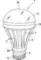
图1及图2揭示了作为照明装置其中之一例的灯泡型的LED灯1。LED灯1具备灯本体2、灯罩(globe)3、E型的灯头4、点灯装置5及COB(chipon board)型的发光装置6。1 and 2 disclose a bulb-
灯本体2例如由铝之类的导热性良好的金属材料构成,兼具作为散热构件的功能。灯本体2为具有一端及另一端的大致圆柱状。多个散热片(fin)7一体地形成在灯本体2的外周面上。散热片7从灯本体2的外周面呈放射状突出,并且,随着从灯本体2的一端向另一端的方向前进,朝向沿着灯本体2的径向的外侧而凸出。其结果,灯本体2的另一端形成为直径较灯本体2的一端还大。The
如图2所示,灯本体2具有第1凹部8及第2凹部9。第1凹部8位于灯本体2的一端,从灯本体2的一端朝向另一端而凹陷。第2凹部9位于灯本体2的另一端,从灯本体2的另一端朝向一端而凹陷。第2凹部9的底成为平坦(flat)的支撑面9a。进而,环(ring)状的段部10设于灯本体2的另一端。段部10包围第2凹部9,并且朝向灯本体2的周围开放。As shown in FIG. 2 , the
灯罩3例如由具有光扩散性的玻璃(glass)或合成树脂材料形成为大致半球形。灯罩3具有球面状的顶部3a及与顶部3a相对的开口部11。开口部11的直径形成为小于灯罩3的最大直径。用来规定开口部11的灯罩3的缘部11a向灯罩3的顶部3a的相反侧而突出,并嵌入至灯本体2的第2凹部9的内侧。其结果,灯罩3结合于灯本体2,并覆盖第2凹部9的支撑面9a。The globe 3 is formed in a substantially hemispherical shape from, for example, light-diffusing glass (glass) or a synthetic resin material. The globe 3 has a spherical top 3 a and an
位于灯本体2的另一端的段部10是与灯罩3之中直径最大的部分的外周部相邻。在段部10上安装着反射环12。反射环12连接灯本体2的另一端的外周缘与灯罩3的外周部之间。The
如图2所示,在灯本体2的第1凹部8内安装着盖体构件14。盖体构件14例如由聚对苯二甲酸乙二醇酯(polyethylene terephthalate,PET)树脂之类的具有电绝缘性的材料构成。盖体构件14具备圆筒状的周壁14a及端壁14b。As shown in FIG. 2 , a
周壁14a嵌入第1凹部8内,并覆盖第1凹部8的内周面。周壁14a具有从第1凹部8突出到灯本体2之外的圆筒状的突出部15。端壁14b堵塞周壁14a的开口端,并且覆盖第1凹部8的底。进而,盖体构件14的内侧的空间通过贯穿灯本体2的通孔(未图示)而连通至灯本体2的支撑面9a。The
灯头4由螺入灯座(lamp socket)内的金属制的外壳(shell)17和具有眼孔(eyelet)端子18的绝缘底座(base)19构成。外壳17以从外侧覆盖该盖体构件14的突出部15的方式而安装在突出部15上。绝缘底座19碰抵到突出部15的开口端部而堵塞盖体构件14的内侧的空间。The
盖体构件14具有从突出部15的外周面凸出的凸缘(flange)部20。凸缘部20是在突出部15的周方向上连续地设置。凸缘部20介在于外壳17的开口端与灯本体2的一端之间,使灯头4与灯本体2之间电性绝缘。The
点灯装置5被收纳于盖体构件14的内侧的空间并与灯头4电性连接。点灯装置5具备四方的电路基板22和安装在电路基板22上的晶体管(transistor)、电阻元件、恒压二极管(diode)、全波整流器及电容器(condenser)之类的多个电路零件23。电路基板22以沿着灯本体2的轴向纵置的姿势而配置在盖体构件14的内侧。The lighting device 5 is accommodated in a space inside the
盖体构件14的内侧并不限于简单地收纳点灯装置5的空间。例如,也可以在盖体构件14的内侧的空间内填充具有散热性及绝缘性的填充材料。作为填充材料,例如可以使用硅酮(silicone)系的树脂材料。填充材料以覆盖点灯装置5的方式而介在于点灯装置5与盖体构件14之间。The inside of the
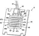
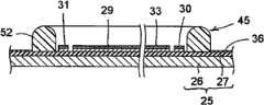
如图2所示,发光装置6被用作LED灯1的光源。发光装置6被安装在灯本体2的支撑面9a上并由灯罩3所覆盖。如图3及图4所示,发光装置6具备矩形状的基板25。基板25由底座26和绝缘层27构成。底座26例如由铝之类的导热性良好且散热性能优异的金属材料形成。当使用绝缘材料来作为构成底座26的材料时,可适用散热特性大致良好且耐久性优异的陶瓷材料或合成树脂材料。绝缘层27例如由环氧(epoxy)树脂之类的具有电绝缘性且为有机材料的合成树脂形成。As shown in FIG. 2 , a
基板25利用多个螺丝而固定在灯本体2的支撑面9a的中央部。藉由该固定,基板25的底座26紧贴于支撑面9a,在基板25与灯本体2之间形成热连接。The
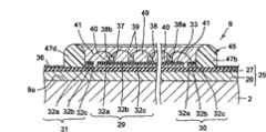
如图5及图6所示,在基板25的绝缘层27上层叠着反光层29、正极侧的第1供电导体30及负极侧的第2供电导体31。反光层29为具有四条边的矩形状,且位于绝缘层27的中央部。进而,反光层29采用了层叠有铜层32a、镀镍层32b及镀银层32c的三层构造。铜层32a是通过对层叠在绝缘层27之上的铜箔进行蚀刻(etching)而形成。镀镍层32b是通过对铜层32a实施无电解电镀而形成。镀银层32c是通过对镀镍层32b实施无电解电镀而形成。镀银层32c包覆镀镍层32b,并且构成反光层29的表层。因此,反光层29的表面成为银色的反光面33。反光面33的总光线反射率例如为90%。As shown in FIGS. 5 and 6 , a
第1供电导体30及第2供电导体31分别具有沿着反光层29的一边而延伸的细长的形状。第1供电导体30及第2供电导体31以夹着反光层29的方式,彼此存在间隔而平行地配置着。第1供电导体30及第2供电导体31分别远离反光层29。因此,第1供电导体30及第2供电导体31相对于反光层29而电性绝缘。The first
第1供电导体30具有朝向远离反光层29的方向而延伸的导体图案(pattern)30a。导体图案30a的前端成为端子部34。同样地,第2供电导体31具有朝向远离反光层29的方向而延伸的导体图案31a。导体图案31b的前端成为端子部35。端子部34、35彼此存在间隔而并列。The first
第1供电导体30及第2供电导体31是与反光层29同时形成于绝缘层27之上,并采用了与反光层29同样的三层构造。即,第1供电导体30及第2供电导体31具有铜层32a、镀镍层32b及镀银层32c,且各自的表层由银构成。The first
第1实施方式中,绝缘层27中的除了反光层29、第1供电导体30、第2供电导体31及端子部34、35以外的区域由抗蚀剂(resist)层36所覆盖。In the first embodiment, the insulating
如图3及图4所示,在反光层29的反光面33上安装着多个发光二极管列37。发光二极管列37朝向与第1供电导体30及第2供电导体31正交的方向而呈直线状延伸,并且彼此存在间隔而平行地排列着。As shown in FIGS. 3 and 4 , on the
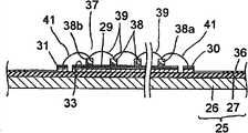
各发光二极管列37具备多个发光二极管芯片38和多条第1接合线39。本实施方式中,作为发光二极管芯片38,例如使用InGaN系的发光元件。发光二极管芯片38具备:具有透光性的蓝宝石(sapphire)基板;以及层叠于蓝宝石基板上并发出蓝色的光的发光层。发光层是通过将n型氮化物半导体层、InGaN发光层和p型氮化物半导体层彼此层叠而构成。Each light emitting
进而,发光二极管芯片38具备对发光层供给电流的正侧电极及负侧电极。正侧电极具有在p型氮化物半导体层上形成的p型电极焊垫(pad)。负侧电极具有在n型氮化物半导体层上形成的n型电极焊垫。Furthermore, the light emitting
发光二极管芯片38分别使用硅酮树脂系的粘合剂40而粘合在反光面33上。进而,发光二极管芯片38在每列发光二极管列37中,在与第1供电导体30及第2供电导体31正交的方向上存在间隔而并列成一列。其结果,多个发光二极管芯片38以遍及反光面33的广范围的方式而呈矩阵(matrix)状规则地排列着。The light emitting
第1接合线39使发光二极管列37延伸的方向上相邻的发光二极管芯片38之间形成电性串联连接。具体而言,第1接合线39跨及发光二极管芯片38之间,以将相邻的发光二极管芯片38的彼此不同极性的电极之间予以连接。The
第1实施方式中,使用金线来作为第1接合线39。与此同时,为了提高第1接合线39的安装强度及降低发光二极管芯片38的损伤,第1接合线39分别经由以Au为主成分的凸块(bump)而连接于正侧电极及负侧电极。In the first embodiment, gold wires are used as the
如图6所示,位于各发光二极管列37的一端及另一端的特定的发光二极管芯片38a、38b分别经由第2接合线41而电性连接于第1供电导体30及第2供电导体31。具体而言,位于各发光二极管列37的一端的发光二极管芯片38a与正极侧的第1供电导体30相邻,并且发光二极管芯片38a的负侧电极经由第2接合线41而电性连接于第1供电导体30。同样地,位于各发光二极管列37的另一端的发光二极管芯片38b与负极侧的第2供电导体31相邻,并且发光二极管芯片38b的正侧电极经由第2接合线41而电性连接于第2供电导体31。因此,多个发光二极管列37相对于第1供电导体30及第2供电导体31而电性并联连接。As shown in FIG. 6 ,
如图3所示,在第1供电导体30及第2供电导体31的端子部34、35上,焊接着连接器(connector)42。连接器42经由导线(lead)43而电性连接于点灯装置5。导线43穿过灯2的通孔而导入至灯头4的内侧的空间。As shown in FIG. 3 , a
当从点灯装置5经由第1供电导体30及第2供电导体31来对多个发光二极管列37供给电流时,发光二极管列37的发光二极管芯片38一齐发光。由于发光二极管列37并联连接于第1供电导体30及第2供电导体31,因此即使因任何理由而导致一个发光二极管列37的发光停止,其他的发光二极管列37仍能够继续发光。When current is supplied from the lighting device 5 to the plurality of light emitting
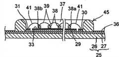
如图3、图4及图6所示,在基板25的绝缘层27上配置着框构件45。框构件45统一包围反光层29、第1供电导体30及第2供电导体31。As shown in FIGS. 3 , 4 and 6 , a
详细而言,框构件45为具有第1角部至第4角部46a、46b、46c、46d以及第1边部至第4边部47a、47b、47c、47d的四方形状。第1边部47a呈直线状而连接第1角部46a与第2角部46b之间。第2边部47b呈直线状而连接第2角部46b与第3角部46c之间。第3边部47c呈直线状而连接第3角部46c与第4角部46d之间。第4边部47d呈直线状而连接第4角部46d与第1角部46a之间。Specifically, the
根据本实施方式,第2边部47b以沿着第1供电导体30的方式而配置,第2边部47b的内表面与第1供电导体30的外侧缘接触。第4边部47d以沿着第2供电导体31的方式而配置,且第4边部47d的内表面与第2供电导体31的外侧缘接触。进而,第1边部47a及第3边部47c与反光层29的外周缘部接触。According to the present embodiment, the
因此,发光二极管芯片38、第1接合线39及第2接合线41位于由框构件45围成的四方区域内。Therefore, the light emitting
框构件45例如通过使用分配器50来将硅酮树脂涂布于基板10上而构成。根据本实施方式,如图8A及图8B所示,在框构件45的第1边部47a的中间部分,配置有重叠涂布硅酮树脂而成的厚壁部48。The
硅酮树脂制的框构件45难以产生因光或热造成的劣化。因此,能够防止表层由银构成的反光层29、第1供电导体30及第2供电导体31的变色。因而,能够良好地维持反光层29、第1供电导体30及第2供电导体31的反射效率。进而,为了进一步抑制反光层29、第1供电导体30及第2供电导体31的表层的变色或劣化,较为理想的是例如使硅酮树脂中含有氧化钛。The
另一方面,若使用环氧树脂来作为构成框构件45的材料,则在反光层29、第1供电导体30及第2供电导体31的表层会附着有机物。其结果,无法避免表层的劣化或变色,从而成为反射效率下降的主要原因。On the other hand, if epoxy resin is used as the material constituting the
密封构件49被填充在由框构件45所围成的区域内。密封构件49例如由具有透光性的透明的硅酮树脂构成。硅酮树脂以液状的状态被注入框构件45的内侧。所注入的硅酮树脂通过加热、干燥而硬化。因此,密封构件49的面积由框构件45来规定。硬化后的密封构件49将反光层29、第1供电导体30、第2供电导体31、发光二极管芯片38、第1接合线39及第2接合线41密封于基板25的绝缘层27之上。The sealing
根据本实施方式,密封构件49含有荧光体。荧光体均等地分散于密封构件49中。作为荧光体,使用受到发光二极管芯片38发出的蓝色的光激发而放射出黄色的光的黄色荧光体。混入至密封构件49中的荧光体并不限于黄色荧光体。例如,为了改善发光二极管芯片38发出的光的显色性,也可以在密封构件49中添加受到蓝色的光激发而发出红色的光的红色荧光体或发出绿色的光的绿色荧光体。According to the present embodiment, the sealing
根据这样的LED灯1,发光二极管芯片38所发出的蓝色的光入射至密封构件49。入射至密封构件49的蓝色的光的一部分被黄色荧光体吸收。剩余的蓝色的光透过密封构件49,而不会被黄色荧光体吸收。According to such an
吸收了蓝色的光的黄色荧光体受到激发而发出黄色的光。黄色的光会透过密封构件49,因此黄色的光与蓝色的光在密封构件49的内部彼此混合而成为白色光。其结果,发光装置6成为放射出白色的光的面状光源。发光装置6所发出的白色光从密封构件49朝向灯罩3而放射,并且透过灯罩3而供照明用途。The yellow phosphor that has absorbed blue light is excited to emit yellow light. Since the yellow light passes through the sealing
透过灯罩3中直径最大的部分而朝向灯本体2的方向的光由反射环(ring)12所反射后,被导向应导出光的方向。进而,从发光二极管芯片38朝向基板25的光被反光层29、第1供电导体30及第2供电导体31的表层所反射后,被导向应导出光的方向。The light passing through the part with the largest diameter in the lampshade 3 and heading toward the
在发光装置6的发光时,发光二极管芯片38所发出的热传递至基板25上的反光层29。反光层29作为使从发光二极管芯片38传递的热得到扩散的散热片(heat spreader)来发挥功能。从反光层29传递至基板25的热进一步经由基板25而传递至灯本体2的支撑面9a。传递至灯本体2的热从散热片7散发到LED灯1之外。When the
其结果,发光二极管芯片38的散热性得到提高,从而能够抑制发光二极管芯片38的过热而良好地维持发光装置6的发光效率。As a result, the heat dissipation of the light-emitting
其次,对于制造发光装置6的工序,参照图7A、图7B、图7C及图7D来进行说明。Next, the process of manufacturing the light-emitting
首先,如图7A所示,在基板25的绝缘层27上形成反光层29、第1供电导体30及第2供电导体31。接着,如图7B所示,在反光层29的反光面33上,将多个发光二极管芯片38呈矩阵状排列并粘合。继而,将相邻的发光二极管芯片38的极性不同的电极之间利用第1接合线39来电性连接。First, as shown in FIG. 7A , the
进而,使位于各发光二极管列37的一端的发光二极管芯片38a的负侧电极与第1供电导体30之间经由第2接合线41而形成电性连接。同样地,使位于各发光二极管列37的另一端的发光二极管芯片38b的正侧电极与第2供电导体31之间经由第2接合线41而形成电性连接。由此,多个发光二极管列37在第1供电导体30与第2供电导体31之间电性并联连接着。Furthermore, the negative electrode of the light emitting
然后,使用分配器50,将具有规定粘度的未硬化的硅酮树脂呈四边形状涂布于基板25的绝缘层27上。硅酮树脂包围电性连接已完成的发光二极管列37、第1供电导体30及第2供电导体31。随后,通过对所涂布的硅酮树脂进行加热来使硅酮树脂硬化,形成如图7C所示的框构件45。Then, using the
继而,如图7D所示,向由框构件45围成的区域内注入液状的硅酮树脂,并且对硅酮树脂进行加热而使其硬化。由此,由框构件45围成的区域被密封构件49填满。将构成框构件45的硅酮树脂涂布于基板25上之后直至使构成密封构件49的硅酮树脂硬化为止的工序是无中断地连续进行。因此,使构成框构件45的硅酮树脂及构成密封构件49的硅酮树脂热硬化的作业能够同时进行。Next, as shown in FIG. 7D , liquid silicone resin is injected into the region surrounded by the
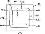
图9A、图9B、图9C、图9D、图9E及图9F表示形成框构件45的顺序。构成框构件45的硅酮树脂52是使用以描绘四边形的轨迹L的方式而移动的分配器50来涂布于基板25之上。为了抑制涂布在基板25上的硅酮树脂52的流动而维持涂布有硅酮树脂52的状态,可使用初始粘度为150Pa·s以上的硅酮树脂52。本实施方式中,使用初始粘度为230Pa·s的硅酮树脂52。9A , 9B, 9C, 9D, 9E, and 9F show the sequence of forming the
根据本实施方式,分配器50沿着轨迹L来开始移动时的起点S例如成为相当于框构件45的第1角部46a的位置。分配器50结束移动的终点E位于分配器50通过起点S后最近的第1边部47a上。因此,在起点S与终点E之间,向基板25上重复供给硅酮树脂52。According to the present embodiment, the starting point S when the
其次,对分配器50所移动的路径进行说明。首先,如图9A所示,分配器50从轨迹L上规定的起点S沿顺时针方向开始移动,对基板25上供给硅酮树脂52。分配器50在轨迹L上移动到相当于框构件45的第2角部46b的位置之后,如图9B所示将移动方向变更90度,对基板25上连续地供给硅酮树脂52。进而,分配器50在轨迹L上移动到相当于框构件45的第3角部46c的位置之后,再次将移动方向变更90度,对基板25上连续地供给硅酮树脂52。继而,分配器50在轨迹L上移动到相当于框构件45的第4角部46d的位置之后,如图9C所示再次将移动方向变更90度,对基板25上连续地供给硅酮树脂52。分配器50在到达轨迹L的起点S之后,如图9D所示再次将移动方向变更90度,且通过起点S之上。分配器50通过起点S之上时,如图9E所示,分配器50被提起,以逐渐远离基板25。分配器50在到达轨迹L上规定的终点E的时刻,停止对基板25供给硅酮树脂。Next, the path along which the
其结果,在轨迹L上的起点S与终点E之间,对基板25上重复涂布硅酮树脂52。因此,如图9F所示,重复涂布有硅酮树脂52的部分成为硅酮树脂52的厚度比其他部分稍许增加的厚壁部48。As a result, the
如上所述,通过从描绘四边形的轨迹L而移动的分配器50来对基板25上供给硅酮树脂52,能够实现在基板25上形成框构件45的工序的自动化。As described above, the process of forming the
进而,本实施方式中,将分配器50开始移动的起点S设为与框构件45的第1角部46a对应的位置,将分配器50停止移动的终点E设为与分配器50通过第1角部45后最近的第1边部47a对应的位置。因此,在从框构件45的第1角部46a到第1边部47a为止的区域,形成重叠涂布硅酮树脂52而成的厚壁部48。该厚壁部48中,硅酮树脂52的厚度比框构件45的其他部分有所增加。因此,构成框构件45的硅酮树脂52在起点S与终点终端E之间不会中断,而能够在周方向上连续地使框构件45紧贴于基板25。Furthermore, in this embodiment, the starting point S at which the
另一方面,在厚壁部48的部位,硅酮树脂52的量有所增加。因此,在直至硅酮树脂52硬化为止的期间内,所涂布的硅酮树脂52有可能会崩塌而以朝向侧方蔓延的方式而流动。但是,由于厚壁部48位于框构件45的第1角部46a的附近,因此即使未硬化的硅酮树脂52发生流动,未硬化的硅酮树脂52亦会表现出朝向框构件45的内侧而蔓延的倾向。因此,未硬化的硅酮树脂52流动的方向得以固定。On the other hand, the amount of the
其结果,能够抑制被填充在框构件45的内侧的密封构件49的厚度尺寸的偏差。因而,从发光二极管芯片38放射出的光的亮度(luminance)及发光色得以稳定。As a result, variation in the thickness dimension of the sealing
与此相对,图10表示将分配器开始移动时的起点S及分配器停止移动时的终点E,设定为与框构件45的第1边部47a的中间对应的位置的比较例。当起点S及终点E位于分配器所描绘的轨迹L的一边的中间时,将无法指定形成厚壁部48的未硬化的硅酮树脂52流动的方向。In contrast, FIG. 10 shows a comparative example in which the start point S when the dispenser starts moving and the end point E when the dispenser stops moving are set at positions corresponding to the middle of the
换言之,未硬化的硅酮树脂52是朝向轨迹L的内侧或外侧蔓延,还是朝向内侧及外侧双方蔓延,易受到涂布硅酮树脂52时的条件所影响。因而,当使起点S及终点E位于轨迹L的一边的中间时,不可否认的是,被填充在框构件45的内侧的密封构件49的厚度尺寸将会产生偏差。In other words, whether the
进而,本发明人在实现形成框构件45的工序的自动化时,改变了发光装置6的制造工序的顺序而尝试了发光装置6的制造。图11A、图11B、图11C及图11D表示变更后的制造工序的一例。与图7A、图7B、图7C及图7D所示的制造工序的不同之处在于,变更后的制造工序在将发光二极管芯片38粘合至反光层29的反光面33而完成电性连接之前,在基板25上形成有框构件45。Furthermore, the present inventors attempted to manufacture the
具体而言,如图11A所示,起先在基板25的绝缘层27上形成反光层29、第1供电导体30及第2供电导体31。继而,如图11B所示,以包围反光层29、第1供电导体30及第2供电导体31的方式,将具有规定粘度的硅酮树脂52涂布于绝缘层27上。随后,使硅酮树脂52硬化,于绝缘层27上形成框构件45。Specifically, as shown in FIG. 11A , first, the
接着,如图11C所示,将多个发光二极管芯片38呈矩阵状排列并粘合于反光层29的反光面33上。继而,使相邻的发光二极管芯片38的极性不同的电极之间利用第1接合线39来电性连接。进而,使位于各发光二极管列37的一端的发光二极管芯片38a的负侧电极与第1供电导体30之间经由第2接合线41而电性连接。同样地,使位于各发光二极管列37的另一端的发光二极管芯片38b的正侧电极与第2供电导体31之间经由第2接合线41而电性连接。Next, as shown in FIG. 11C , a plurality of
随后,如图11D所示,向由框构件45围成的区域内注入液状的硅酮树脂,并且对硅酮树脂进行加热而使其硬化。由此,由框构件45所围成的区域被密封构件49填满。Subsequently, as shown in FIG. 11D , liquid silicone resin is injected into the region surrounded by the
试行此种制造方法的结果明确了以下所述的问题。The results of trials of this manufacturing method identified the problems described below.
(I)难以将第2接合线41连接于第1供电导体30及第2供电导体31。即使完成接合,第2接合线41对第1供电导体30及第2供电导体31的接合强度也不够充分,接合的可靠性及稳定性下降。考虑其原因是因为,在为了使构成框构件45的硅酮树脂52硬化而进行加热时,硅酮树脂52中的硅氧烷(siloxane)发生扩散,扩散的硅氧烷附着于第1供电导体30及第2供电导体31的表层而妨碍到第2接合线42的接合。(I) It is difficult to connect the
(II)若不对涂布在绝缘层27上的硅酮树脂52进行加热而放置30分钟以上,则由于兼顾了硅酮树脂52的粘度,因此未硬化的硅酮树脂52会以蔓延的方式而流动。流动的未硬化的硅酮树脂52到达第1供电导体30或第2供电导体31的表层,而附着于成为表层的银上。其结果,第1供电导体30及第2供电导体31受到污染,附着在第1供电导体30及第2供电导体31上的硅酮树脂52成为妨碍第2接合线42的接合的主要原因。(II) If the
(III)如图11C所示,必须在框构件45与第1供电导体30以及框构件45与第2供电导体31之间分别确保间隙g,以使得框构件45不会妨碍将第2接合线42连接于第1供电导体30及第2供电导体31的作业。因此,无助于光的反射的绝缘层27会通过间隙g而露出到由框构件45所围成的区域上,从而对光的反射效率造成不良影响。(III) As shown in FIG. 11C , it is necessary to ensure a gap g between the
由以上所述获得下述见解:在实现形成框构件45的工序的自动化时,图7A、图7B、图7C及图7D所示的制造工序最佳,由此,能够确保第2接合线42对第1供电导体30及第2供电导体31的接合强度、接合的可靠性及稳定性。From the above, the following insight is obtained: when realizing the automation of the process of forming the
进而,根据图7A、图7B、图7C及图7D所示的制造工序,能够使框构件45接触第1供电导体30及第2供电导体31。因此,能够防止无助于光的反射的绝缘层27从框构件45与第1供电导体30以及框构件45与第2供电导体45之间露出。因而,能够有效地利用第1供电导体30及第2供电导体31的银的表层来提高光的反射效率。Furthermore, according to the manufacturing steps shown in FIGS. 7A , 7B, 7C, and 7D, the
所述实施方式的发光二极管列中,将相邻的发光二极管芯片之间经由第1接合线而直接连接。但是,也可以将相邻的发光二极管芯片之间经由基板上形成的配线图案而连接。In the light emitting diode array of the above embodiment, adjacent light emitting diode chips are directly connected via the first bonding wire. However, adjacent light emitting diode chips may be connected via a wiring pattern formed on the substrate.
框构件并不限于四边形,例如只要是三角形、五边形或六边形之类的多边形即可。除此以外,所谓多边形,也包括使多个角部为弧形(round),连接角部之间的边部稍许弯曲的情况。The frame member is not limited to a quadrangle, and may be any polygon such as a triangle, pentagon, or hexagon, for example. In addition, the term "polygon" also includes a case where a plurality of corners are rounded and a side connecting the corners is slightly curved.
进而,对于照明装置,并不限于LED灯,例如在室内或室外使用的聚光灯(spotlight)或路灯也可同样适用。Furthermore, the lighting device is not limited to LED lamps, and for example, spotlights or street lamps used indoors or outdoors are also applicable.
以上所述,仅是本发明的较佳实施例而已,并非对本发明作任何形式上的限制,虽然本发明已以较佳实施例揭露如上,然而并非用以限定本发明,任何熟悉本专业的技术人员,在不脱离本发明技术方案范围内,当可利用上述揭示的技术内容作出些许更动或修饰为等同变化的等效实施例,但凡是未脱离本发明技术方案的内容,依据本发明的技术实质对以上实施例所作的任何简单修改、等同变化与修饰,均仍属于本发明技术方案的范围内。The above description is only a preferred embodiment of the present invention, and does not limit the present invention in any form. Although the present invention has been disclosed as above with preferred embodiments, it is not intended to limit the present invention. Anyone familiar with this field Those skilled in the art, without departing from the scope of the technical solution of the present invention, can use the technical content disclosed above to make some changes or modify equivalent embodiments with equivalent changes, but all the content that does not depart from the technical solution of the present invention, according to the present invention Any simple modifications, equivalent changes and modifications made to the above embodiments by the technical essence still belong to the scope of the technical solution of the present invention.
Claims (4)
Applications Claiming Priority (2)
| Application Number | Priority Date | Filing Date | Title |
|---|---|---|---|
| JP2009-219771 | 2009-09-24 | ||
| JP2009219771AJP2011071242A (en) | 2009-09-24 | 2009-09-24 | Light emitting device and illuminating device |
Publications (2)
| Publication Number | Publication Date |
|---|---|
| CN102034924A CN102034924A (en) | 2011-04-27 |
| CN102034924Btrue CN102034924B (en) | 2013-05-22 |
Family
ID=43480483
Family Applications (1)
| Application Number | Title | Priority Date | Filing Date |
|---|---|---|---|
| CN2010102864240AExpired - Fee RelatedCN102034924B (en) | 2009-09-24 | 2010-09-17 | Lighting devices and lighting devices |
Country Status (4)
| Country | Link |
|---|---|
| US (1) | US8354783B2 (en) |
| EP (1) | EP2302283A3 (en) |
| JP (1) | JP2011071242A (en) |
| CN (1) | CN102034924B (en) |
Families Citing this family (55)
| Publication number | Priority date | Publication date | Assignee | Title |
|---|---|---|---|---|
| US7758223B2 (en) | 2005-04-08 | 2010-07-20 | Toshiba Lighting & Technology Corporation | Lamp having outer shell to radiate heat of light source |
| CN103470983A (en) | 2008-06-27 | 2013-12-25 | 东芝照明技术株式会社 | Light-emitting element lamp and lighting equipment |
| JP5333758B2 (en) | 2009-02-27 | 2013-11-06 | 東芝ライテック株式会社 | Lighting device and lighting fixture |
| JP2011049527A (en)* | 2009-07-29 | 2011-03-10 | Toshiba Lighting & Technology Corp | Led lighting equipment |
| JP5601512B2 (en) | 2009-09-14 | 2014-10-08 | 東芝ライテック株式会社 | Light emitting device and lighting device |
| US8678618B2 (en) | 2009-09-25 | 2014-03-25 | Toshiba Lighting & Technology Corporation | Self-ballasted lamp having a light-transmissive member in contact with light emitting elements and lighting equipment incorporating the same |
| US8324789B2 (en) | 2009-09-25 | 2012-12-04 | Toshiba Lighting & Technology Corporation | Self-ballasted lamp and lighting equipment |
| CN102032481B (en) | 2009-09-25 | 2014-01-08 | 东芝照明技术株式会社 | Lighting lamps and lighting fixtures with sockets |
| JP2011091033A (en) | 2009-09-25 | 2011-05-06 | Toshiba Lighting & Technology Corp | Light-emitting module, bulb-shaped lamp and lighting equipment |
| JP2011204897A (en)* | 2010-03-25 | 2011-10-13 | Toshiba Lighting & Technology Corp | Light emitting module |
| JP5612991B2 (en)* | 2010-09-30 | 2014-10-22 | シャープ株式会社 | LIGHT EMITTING DEVICE AND LIGHTING DEVICE HAVING THE SAME |
| USD721339S1 (en) | 2010-12-03 | 2015-01-20 | Cree, Inc. | Light emitter device |
| US8564000B2 (en) | 2010-11-22 | 2013-10-22 | Cree, Inc. | Light emitting devices for light emitting diodes (LEDs) |
| USD712850S1 (en) | 2010-11-18 | 2014-09-09 | Cree, Inc. | Light emitter device |
| USD707192S1 (en) | 2010-11-18 | 2014-06-17 | Cree, Inc. | Light emitting device |
| US9490235B2 (en)* | 2010-11-22 | 2016-11-08 | Cree, Inc. | Light emitting devices, systems, and methods |
| US9300062B2 (en) | 2010-11-22 | 2016-03-29 | Cree, Inc. | Attachment devices and methods for light emitting devices |
| US8575639B2 (en) | 2011-02-16 | 2013-11-05 | Cree, Inc. | Light emitting devices for light emitting diodes (LEDs) |
| US8624271B2 (en) | 2010-11-22 | 2014-01-07 | Cree, Inc. | Light emitting devices |
| US9000470B2 (en)* | 2010-11-22 | 2015-04-07 | Cree, Inc. | Light emitter devices |
| USD706231S1 (en) | 2010-12-03 | 2014-06-03 | Cree, Inc. | Light emitting device |
| USD702653S1 (en) | 2011-10-26 | 2014-04-15 | Cree, Inc. | Light emitting device component |
| US8809880B2 (en) | 2011-02-16 | 2014-08-19 | Cree, Inc. | Light emitting diode (LED) chips and devices for providing failure mitigation in LED arrays |
| US8455908B2 (en) | 2011-02-16 | 2013-06-04 | Cree, Inc. | Light emitting devices |
| KR102028594B1 (en) | 2011-04-26 | 2019-10-04 | 산유 레크 가부시키가이샤 | Method and apparatus for manufacturing optical device |
| CN107768502B (en)* | 2011-05-16 | 2019-07-05 | 日亚化学工业株式会社 | Light-emitting device and method of manufacturing the same |
| JP5833850B2 (en)* | 2011-07-08 | 2015-12-16 | シチズン電子株式会社 | Semiconductor light emitting device and manufacturing method thereof |
| JP2013026416A (en)* | 2011-07-20 | 2013-02-04 | Toyoda Gosei Co Ltd | Element mounting substrate and light emitting device including the same |
| USD705181S1 (en) | 2011-10-26 | 2014-05-20 | Cree, Inc. | Light emitting device component |
| JP5378481B2 (en)* | 2011-11-04 | 2013-12-25 | 胡文松 | High illumination LED bulb with 360 degree shot angle |
| KR20140097284A (en) | 2011-11-07 | 2014-08-06 | 크리,인코포레이티드 | High voltage array light emitting diode(led) devices, fixtures and methods |
| CN104115291A (en)* | 2012-02-13 | 2014-10-22 | 克利公司 | Improved light emitting device and method |
| JP5847619B2 (en)* | 2012-03-14 | 2016-01-27 | シャープ株式会社 | Light emitting device and lighting device |
| US10134961B2 (en) | 2012-03-30 | 2018-11-20 | Cree, Inc. | Submount based surface mount device (SMD) light emitter components and methods |
| US9735198B2 (en) | 2012-03-30 | 2017-08-15 | Cree, Inc. | Substrate based light emitter devices, components, and related methods |
| USD708155S1 (en)* | 2012-04-20 | 2014-07-01 | Cree, Inc. | Solid state lighting apparatus |
| JP6065408B2 (en)* | 2012-04-27 | 2017-01-25 | 日亜化学工業株式会社 | Light emitting device and manufacturing method thereof |
| DE102012106982A1 (en) | 2012-07-31 | 2014-02-06 | Osram Opto Semiconductors Gmbh | Process for the production of a light source |
| JP6019906B2 (en)* | 2012-08-07 | 2016-11-02 | 日亜化学工業株式会社 | Light emitting device and manufacturing method thereof |
| JP6024957B2 (en)* | 2012-09-24 | 2016-11-16 | 東芝ライテック株式会社 | Light emitting device and lighting device |
| US9029880B2 (en)* | 2012-12-10 | 2015-05-12 | LuxVue Technology Corporation | Active matrix display panel with ground tie lines |
| US9178123B2 (en) | 2012-12-10 | 2015-11-03 | LuxVue Technology Corporation | Light emitting device reflective bank structure |
| US9159700B2 (en) | 2012-12-10 | 2015-10-13 | LuxVue Technology Corporation | Active matrix emissive micro LED display |
| JP2014130916A (en)* | 2012-12-28 | 2014-07-10 | Toshiba Lighting & Technology Corp | Substrate for light-emitting module and method of manufacturing substrate for light-emitting module |
| US9033544B2 (en)* | 2013-04-19 | 2015-05-19 | Technical Consumer Products, Inc. | Smooth LED PAR lamp |
| TWI651871B (en)* | 2013-06-27 | 2019-02-21 | 晶元光電股份有限公司 | Light-emitting component and manufacturing method |
| USD739565S1 (en) | 2013-06-27 | 2015-09-22 | Cree, Inc. | Light emitter unit |
| USD740453S1 (en) | 2013-06-27 | 2015-10-06 | Cree, Inc. | Light emitter unit |
| WO2015050164A1 (en)* | 2013-10-03 | 2015-04-09 | シャープ株式会社 | Substrate for light-emitting device, light-emitting device, and method for producing substrate for light-emitting device |
| DE102016201917A1 (en)* | 2016-02-09 | 2017-08-10 | Tridonic Jennersdorf Gmbh | LED light source with higher protection class |
| USD823492S1 (en) | 2016-10-04 | 2018-07-17 | Cree, Inc. | Light emitting device |
| CN206918825U (en)* | 2017-04-25 | 2018-01-23 | 漳州立达信光电子科技有限公司 | A split downlight |
| JP6512316B2 (en)* | 2018-01-19 | 2019-05-15 | 日亜化学工業株式会社 | Light emitting device |
| JP6879270B2 (en)* | 2018-07-20 | 2021-06-02 | 日亜化学工業株式会社 | Light emitting device |
| JP7240907B2 (en)* | 2019-03-12 | 2023-03-16 | シチズン電子株式会社 | Light-emitting device and method for manufacturing light-emitting device |
Citations (1)
| Publication number | Priority date | Publication date | Assignee | Title |
|---|---|---|---|---|
| CN101266968A (en)* | 2007-03-15 | 2008-09-17 | 夏普株式会社 | Light emitting device and method of manufacturing the same |
Family Cites Families (171)
| Publication number | Priority date | Publication date | Assignee | Title |
|---|---|---|---|---|
| US534665A (en)* | 1895-02-26 | Method of casting projectiles | ||
| US356107A (en)* | 1887-01-18 | Ella b | ||
| US534038A (en)* | 1895-02-12 | Dynamo-electric machine | ||
| US1972790A (en) | 1932-07-15 | 1934-09-04 | Crouse Hinds Co | Electric hand lamp |
| GB1601461A (en)* | 1977-05-21 | 1981-10-28 | Amp Inc | Electrical junction box |
| US4503360A (en) | 1982-07-26 | 1985-03-05 | North American Philips Lighting Corporation | Compact fluorescent lamp unit having segregated air-cooling means |
| JPH071374B2 (en)* | 1984-03-06 | 1995-01-11 | 株式会社ニコン | Light source |
| US4939420A (en)* | 1987-04-06 | 1990-07-03 | Lim Kenneth S | Fluorescent reflector lamp assembly |
| USD356107S (en) | 1992-05-15 | 1995-03-07 | Fujitsu Limited | Developing cartridge for copier |
| JP3121916B2 (en) | 1992-06-25 | 2001-01-09 | 矢橋工業株式会社 | Method for producing lime sintered body |
| DE4235289C2 (en) | 1992-10-20 | 1996-08-01 | Teves Gmbh Alfred | Signal light for a vehicle |
| US5323271A (en) | 1992-11-24 | 1994-06-21 | Equestrian Co., Ltd. | Water- and air-cooled reflection mirror |
| JP2662488B2 (en)* | 1992-12-04 | 1997-10-15 | 株式会社小糸製作所 | Seal structure between front lens leg and seal groove in automotive lighting |
| US5327332A (en)* | 1993-04-29 | 1994-07-05 | Hafemeister Beverly J | Decorative light socket extension |
| JP2828584B2 (en) | 1993-12-27 | 1998-11-25 | 株式会社小糸製作所 | Automotive headlamp |
| US5632551A (en)* | 1994-07-18 | 1997-05-27 | Grote Industries, Inc. | LED vehicle lamp assembly |
| US5537301A (en)* | 1994-09-01 | 1996-07-16 | Pacific Scientific Company | Fluorescent lamp heat-dissipating apparatus |
| US5585697A (en)* | 1994-11-17 | 1996-12-17 | General Electric Company | PAR lamp having an integral photoelectric circuit arrangement |
| US6465743B1 (en)* | 1994-12-05 | 2002-10-15 | Motorola, Inc. | Multi-strand substrate for ball-grid array assemblies and method |
| CA2225734C (en) | 1995-06-29 | 2006-11-14 | Lynn Wiese | Localized illumination using tir technology |
| US6111359A (en) | 1996-05-09 | 2000-08-29 | Philips Electronics North America Corporation | Integrated HID reflector lamp with HID arc tube in a pressed glass reflector retained in a shell housing a ballast |
| US6095668A (en)* | 1996-06-19 | 2000-08-01 | Radiant Imaging, Inc. | Incandescent visual display system having a shaped reflector |
| US5785418A (en)* | 1996-06-27 | 1998-07-28 | Hochstein; Peter A. | Thermally protected LED array |
| US5857767A (en)* | 1996-09-23 | 1999-01-12 | Relume Corporation | Thermal management system for L.E.D. arrays |
| JPH1125919A (en)* | 1997-07-04 | 1999-01-29 | Moriyama Sangyo Kk | Electric bulb device and lighting system |
| US5947588A (en) | 1997-10-06 | 1999-09-07 | Grand General Accessories Manufacturing Inc. | Light fixture with an LED light bulb having a conventional connection post |
| JP2000083343A (en) | 1998-09-03 | 2000-03-21 | Mitsubishi Electric Corp | Motor frame and method of manufacturing motor frame |
| WO2000017569A1 (en) | 1998-09-17 | 2000-03-30 | Koninklijke Philips Electronics N.V. | Led lamp |
| JP3753291B2 (en) | 1998-09-30 | 2006-03-08 | 東芝ライテック株式会社 | Light bulb shaped fluorescent lamp |
| US6502968B1 (en)* | 1998-12-22 | 2003-01-07 | Mannesmann Vdo Ag | Printed circuit board having a light source |
| US6186646B1 (en)* | 1999-03-24 | 2001-02-13 | Hinkley Lighting Incorporated | Lighting fixture having three sockets electrically connected and mounted to bowl and cover plate |
| JP2000294434A (en)* | 1999-04-02 | 2000-10-20 | Hanshin Electric Co Ltd | Internal combustion engine ignition coil |
| US6227679B1 (en) | 1999-09-16 | 2001-05-08 | Mule Lighting Inc | Led light bulb |
| US6525455B1 (en) | 1999-09-22 | 2003-02-25 | Matsushita Electric Industrial Co., Ltd. | Bulb-form lamp and its manufacturing method |
| US6161910A (en)* | 1999-12-14 | 2000-12-19 | Aerospace Lighting Corporation | LED reading light |
| JP2001243809A (en) | 2000-02-28 | 2001-09-07 | Mitsubishi Electric Lighting Corp | Led electric bulb |
| US6814470B2 (en)* | 2000-05-08 | 2004-11-09 | Farlight Llc | Highly efficient LED lamp |
| US6626554B2 (en)* | 2000-05-18 | 2003-09-30 | Aaron Nathan Rincover | Light apparatus |
| US7122900B2 (en)* | 2000-06-26 | 2006-10-17 | Renesas Technology Corp. | Semiconductor device and method manufacturing the same |
| JP2002075011A (en)* | 2000-08-30 | 2002-03-15 | Matsushita Electric Ind Co Ltd | Tube ball |
| US6517217B1 (en)* | 2000-09-18 | 2003-02-11 | Hwa Hsia Glass Co., Ltd. | Ornamental solar lamp assembly |
| US6357902B1 (en) | 2000-09-25 | 2002-03-19 | Brian Horowitz | After market LED taillight bulb |
| KR20020091173A (en) | 2001-02-02 | 2002-12-05 | 코닌클리즈케 필립스 일렉트로닉스 엔.브이. | Integrated light source |
| JP2002280617A (en) | 2001-03-19 | 2002-09-27 | Matsushita Electric Ind Co Ltd | Lighting equipment |
| US6598996B1 (en) | 2001-04-27 | 2003-07-29 | Pervaiz Lodhie | LED light bulb |
| CN2489462Y (en) | 2001-06-17 | 2002-05-01 | 广东伟雄集团有限公司 | Energy-saving lamp with insert strip |
| JP4674418B2 (en) | 2001-06-29 | 2011-04-20 | パナソニック株式会社 | Lighting equipment |
| JP4076329B2 (en) | 2001-08-13 | 2008-04-16 | エイテックス株式会社 | LED bulb |
| JP4193446B2 (en)* | 2001-08-22 | 2008-12-10 | 日亜化学工業株式会社 | Light emitting device |
| US6866401B2 (en) | 2001-12-21 | 2005-03-15 | General Electric Company | Zoomable spot module |
| US6682211B2 (en) | 2001-09-28 | 2004-01-27 | Osram Sylvania Inc. | Replaceable LED lamp capsule |
| JP2003115203A (en) | 2001-10-03 | 2003-04-18 | Matsushita Electric Ind Co Ltd | Low pressure mercury vapor discharge lamp and method of manufacturing the same |
| US6525668B1 (en)* | 2001-10-10 | 2003-02-25 | Twr Lighting, Inc. | LED array warning light system |
| US6942365B2 (en)* | 2002-12-10 | 2005-09-13 | Robert Galli | LED lighting assembly |
| EP1467414A4 (en)* | 2001-12-29 | 2007-07-11 | Hangzhou Fuyang Xinying Dianzi | A led and led lamp |
| US6936855B1 (en)* | 2002-01-16 | 2005-08-30 | Shane Harrah | Bendable high flux LED array |
| US6685339B2 (en) | 2002-02-14 | 2004-02-03 | Polaris Pool Systems, Inc. | Sparkle light bulb with controllable memory function |
| US6641283B1 (en) | 2002-04-12 | 2003-11-04 | Gelcore, Llc | LED puck light with detachable base |
| CN1264152C (en) | 2002-05-08 | 2006-07-12 | 国硕科技工业股份有限公司 | High Density Recordable Optical Recording Media |
| US6824296B2 (en) | 2002-07-02 | 2004-11-30 | Leviton Manufacturing Co., Inc. | Night light assembly |
| US20040012955A1 (en)* | 2002-07-17 | 2004-01-22 | Wen-Chang Hsieh | Flashlight |
| JP4123886B2 (en) | 2002-09-24 | 2008-07-23 | 東芝ライテック株式会社 | LED lighting device |
| US6787999B2 (en) | 2002-10-03 | 2004-09-07 | Gelcore, Llc | LED-based modular lamp |
| JP2004140185A (en)* | 2002-10-17 | 2004-05-13 | Matsushita Electric Ind Co Ltd | Light emitting device |
| US7111961B2 (en) | 2002-11-19 | 2006-09-26 | Automatic Power, Inc. | High flux LED lighting device |
| US7188980B2 (en)* | 2002-12-02 | 2007-03-13 | Honda Motor Co., Ltd. | Head light system |
| US7153004B2 (en)* | 2002-12-10 | 2006-12-26 | Galli Robert D | Flashlight housing |
| JP2004193053A (en) | 2002-12-13 | 2004-07-08 | Toshiba Lighting & Technology Corp | Compact fluorescent lamps and lighting equipment |
| US6964501B2 (en)* | 2002-12-24 | 2005-11-15 | Altman Stage Lighting Co., Ltd. | Peltier-cooled LED lighting assembly |
| JP4038136B2 (en) | 2003-01-13 | 2008-01-23 | シーシーエス株式会社 | Spot lighting device using power LED |
| EP1447619A1 (en)* | 2003-02-12 | 2004-08-18 | Exterieur Vert S.A. | Lighting device, in particular projector-like sealed luminaire recessed in the ground, cooled by air circulation |
| CN2637885Y (en) | 2003-02-20 | 2004-09-01 | 高勇 | LED lamp bulb with luminous curved surface |
| JP3885032B2 (en)* | 2003-02-28 | 2007-02-21 | 松下電器産業株式会社 | Fluorescent lamp |
| AU2003902031A0 (en) | 2003-04-29 | 2003-05-15 | Eveready Battery Company, Inc | Lighting device |
| US6921181B2 (en)* | 2003-07-07 | 2005-07-26 | Mei-Feng Yen | Flashlight with heat-dissipation device |
| US7679096B1 (en)* | 2003-08-21 | 2010-03-16 | Opto Technology, Inc. | Integrated LED heat sink |
| US7300173B2 (en) | 2004-04-08 | 2007-11-27 | Technology Assessment Group, Inc. | Replacement illumination device for a miniature flashlight bulb |
| US7329024B2 (en)* | 2003-09-22 | 2008-02-12 | Permlight Products, Inc. | Lighting apparatus |
| US6942360B2 (en)* | 2003-10-01 | 2005-09-13 | Enertron, Inc. | Methods and apparatus for an LED light engine |
| US6982518B2 (en)* | 2003-10-01 | 2006-01-03 | Enertron, Inc. | Methods and apparatus for an LED light |
| US7144135B2 (en)* | 2003-11-26 | 2006-12-05 | Philips Lumileds Lighting Company, Llc | LED lamp heat sink |
| JP2005166578A (en) | 2003-12-05 | 2005-06-23 | Hamai Denkyu Kogyo Kk | Light bulb shaped LED lamp |
| US7281818B2 (en)* | 2003-12-11 | 2007-10-16 | Dialight Corporation | Light reflector device for light emitting diode (LED) array |
| US7198387B1 (en)* | 2003-12-18 | 2007-04-03 | B/E Aerospace, Inc. | Light fixture for an LED-based aircraft lighting system |
| USD497439S1 (en) | 2003-12-24 | 2004-10-19 | Elumina Technolgy Incorporation | Lamp with high power LED |
| JP4343720B2 (en) | 2004-01-23 | 2009-10-14 | 株式会社小糸製作所 | Lamp |
| US6948829B2 (en)* | 2004-01-28 | 2005-09-27 | Dialight Corporation | Light emitting diode (LED) light bulbs |
| JP2005217354A (en) | 2004-02-02 | 2005-08-11 | Sumitomo Wiring Syst Ltd | Light emitting device unit |
| JP2005286267A (en) | 2004-03-31 | 2005-10-13 | Hitachi Lighting Ltd | Light emitting diode lamp |
| US7059748B2 (en) | 2004-05-03 | 2006-06-13 | Osram Sylvania Inc. | LED bulb |
| US7367692B2 (en) | 2004-04-30 | 2008-05-06 | Lighting Science Group Corporation | Light bulb having surfaces for reflecting light produced by electronic light generating sources |
| TWI257991B (en)* | 2004-05-12 | 2006-07-11 | Kun-Lieh Huang | Lighting device with auxiliary heat dissipation functions |
| US7125146B2 (en)* | 2004-06-30 | 2006-10-24 | H-Tech, Inc. | Underwater LED light |
| WO2006013493A2 (en)* | 2004-07-27 | 2006-02-09 | Koninklijke Philips Electronics N.V. | Integrated reflector lamp |
| JP2006040727A (en) | 2004-07-27 | 2006-02-09 | Matsushita Electric Works Ltd | Light-emitting diode lighting device and illumination device |
| US20060034077A1 (en) | 2004-08-10 | 2006-02-16 | Tsu-Kang Chang | White light bulb assembly using LED as a light source |
| DE102004042186B4 (en)* | 2004-08-31 | 2010-07-01 | Osram Opto Semiconductors Gmbh | Optoelectronic component |
| US7165866B2 (en)* | 2004-11-01 | 2007-01-23 | Chia Mao Li | Light enhanced and heat dissipating bulb |
| JP2005123200A (en) | 2004-11-04 | 2005-05-12 | Toshiba Lighting & Technology Corp | Light bulb shaped fluorescent lamp |
| JP2006156187A (en) | 2004-11-30 | 2006-06-15 | Mitsubishi Electric Corp | LED light source device and LED bulb |
| JP3787148B1 (en) | 2005-09-06 | 2006-06-21 | 株式会社未来 | Lighting unit and lighting device |
| US7144140B2 (en)* | 2005-02-25 | 2006-12-05 | Tsung-Ting Sun | Heat dissipating apparatus for lighting utility |
| JP2006244725A (en) | 2005-02-28 | 2006-09-14 | Atex Co Ltd | Led lighting system |
| US7255460B2 (en) | 2005-03-23 | 2007-08-14 | Nuriplan Co., Ltd. | LED illumination lamp |
| JP2006278774A (en) | 2005-03-29 | 2006-10-12 | Hitachi Cable Ltd | Method for manufacturing double-sided wiring board, double-sided wiring board, and base board thereof |
| NL1028678C2 (en) | 2005-04-01 | 2006-10-03 | Lemnis Lighting Ip Gmbh | Heat sink, lamp and method for manufacturing a heat sink. |
| JP4725231B2 (en) | 2005-04-08 | 2011-07-13 | 東芝ライテック株式会社 | Light bulb lamp |
| CN101660740B (en) | 2005-04-08 | 2013-03-13 | 东芝照明技术株式会社 | Lamp |
| JP4482706B2 (en) | 2005-04-08 | 2010-06-16 | 東芝ライテック株式会社 | Light bulb lamp |
| US7758223B2 (en) | 2005-04-08 | 2010-07-20 | Toshiba Lighting & Technology Corporation | Lamp having outer shell to radiate heat of light source |
| USD534665S1 (en) | 2005-04-15 | 2007-01-02 | Toshiba Lighting & Technology Corporation | Light emitting diode lamp |
| US7226189B2 (en)* | 2005-04-15 | 2007-06-05 | Taiwan Oasis Technology Co., Ltd. | Light emitting diode illumination apparatus |
| USD535038S1 (en) | 2005-04-15 | 2007-01-09 | Toshiba Lighting & Technology Corporation | Light emitting diode lamp |
| JP2006310057A (en) | 2005-04-27 | 2006-11-09 | Arumo Technos Kk | Led illumination lamp and led lighting control circuit |
| US7744256B2 (en) | 2006-05-22 | 2010-06-29 | Edison Price Lighting, Inc. | LED array wafer lighting fixture |
| EP2287526B1 (en)* | 2005-07-20 | 2013-09-11 | TBT Asset Management International Limited | Illumination unit with serpentine-shaped cold cathode fluorescent lamp |
| WO2007030542A2 (en) | 2005-09-06 | 2007-03-15 | Lsi Industries, Inc. | Linear lighting system |
| JP4715422B2 (en)* | 2005-09-27 | 2011-07-06 | 日亜化学工業株式会社 | Light emitting device |
| US20070103904A1 (en)* | 2005-11-09 | 2007-05-10 | Ching-Chao Chen | Light emitting diode lamp |
| JP2007188832A (en) | 2006-01-16 | 2007-07-26 | Toshiba Lighting & Technology Corp | lamp |
| JP2007207576A (en) | 2006-02-01 | 2007-08-16 | Jefcom Kk | Led lamp |
| WO2007142946A2 (en) | 2006-05-31 | 2007-12-13 | Cree Led Lighting Solutions, Inc. | Lighting device and method of lighting |
| US7824075B2 (en)* | 2006-06-08 | 2010-11-02 | Lighting Science Group Corporation | Method and apparatus for cooling a lightbulb |
| TWM309051U (en) | 2006-06-12 | 2007-04-01 | Grand Halo Technology Co Ltd | Light-emitting device |
| JP4300223B2 (en)* | 2006-06-30 | 2009-07-22 | 株式会社 日立ディスプレイズ | LIGHTING DEVICE AND DISPLAY DEVICE USING LIGHTING DEVICE |
| JP4367457B2 (en) | 2006-07-06 | 2009-11-18 | パナソニック電工株式会社 | Silver film, silver film manufacturing method, LED mounting substrate, and LED mounting substrate manufacturing method |
| US7922359B2 (en) | 2006-07-17 | 2011-04-12 | Liquidleds Lighting Corp. | Liquid-filled LED lamp with heat dissipation means |
| US7396146B2 (en)* | 2006-08-09 | 2008-07-08 | Augux Co., Ltd. | Heat dissipating LED signal lamp source structure |
| CN101128041B (en) | 2006-08-15 | 2010-05-12 | 华为技术有限公司 | Method and system for processing failure of downlink data tunnel between access network and core network |
| TW200837308A (en) | 2006-09-21 | 2008-09-16 | Led Lighting Fixtures Inc | Lighting assemblies, methods of installing same, and methods of replacing lights |
| US20080080187A1 (en) | 2006-09-28 | 2008-04-03 | Purinton Richard S | Sealed LED light bulb |
| KR101513738B1 (en) | 2006-11-14 | 2015-04-21 | 크리, 인코포레이티드 | Lighting assemblies and components for lighting assemblies |
| KR101408613B1 (en) | 2006-11-30 | 2014-06-20 | 크리, 인코포레이티드 | Self-ballasted solid state lighting devices |
| US20110128742A9 (en)* | 2007-01-07 | 2011-06-02 | Pui Hang Yuen | High efficiency low cost safety light emitting diode illumination device |
| US7968900B2 (en)* | 2007-01-19 | 2011-06-28 | Cree, Inc. | High performance LED package |
| JP2008277561A (en) | 2007-04-27 | 2008-11-13 | Toshiba Lighting & Technology Corp | Lighting device |
| CN101307887A (en) | 2007-05-14 | 2008-11-19 | 穆学利 | LED lighting bulb |
| EP2163808B1 (en) | 2007-05-23 | 2014-04-23 | Sharp Kabushiki Kaisha | Lighting device |
| US8403531B2 (en)* | 2007-05-30 | 2013-03-26 | Cree, Inc. | Lighting device and method of lighting |
| JP5029893B2 (en) | 2007-07-06 | 2012-09-19 | 東芝ライテック株式会社 | Light bulb shaped LED lamp and lighting device |
| CN101883946A (en) | 2007-08-22 | 2010-11-10 | 量子跃进研究公司 | Lighting assemblies comprising multiple light sources with play and associated height control mechanisms |
| JP2009081349A (en)* | 2007-09-27 | 2009-04-16 | Toshiba Lighting & Technology Corp | Lighting device |
| WO2009048951A2 (en)* | 2007-10-09 | 2009-04-16 | Philips Solid-State Lighting Solutions | Methods and apparatus for controlling respective load currents of multiple series-connected loads |
| JP2011501417A (en)* | 2007-10-10 | 2011-01-06 | クリー エル イー ディー ライティング ソリューションズ インコーポレイテッド | Lighting device and manufacturing method |
| JP4569683B2 (en) | 2007-10-16 | 2010-10-27 | 東芝ライテック株式会社 | Light emitting element lamp and lighting apparatus |
| JP2009135485A (en)* | 2007-11-07 | 2009-06-18 | Mitsubishi Chemicals Corp | Semiconductor light emitting device and manufacturing method thereof |
| DE102007055133A1 (en) | 2007-11-19 | 2009-05-20 | Osram Gesellschaft mit beschränkter Haftung | Lighting device with a heat sink |
| JP2009135026A (en) | 2007-11-30 | 2009-06-18 | Toshiba Lighting & Technology Corp | LED lighting fixtures |
| US7625104B2 (en) | 2007-12-13 | 2009-12-01 | Philips Lumileds Lighting Company, Llc | Light emitting diode for mounting to a heat sink |
| US20090184646A1 (en) | 2007-12-21 | 2009-07-23 | John Devaney | Light emitting diode cap lamp |
| US8049237B2 (en)* | 2007-12-28 | 2011-11-01 | Nichia Corporation | Light emitting device |
| JP5119917B2 (en)* | 2007-12-28 | 2013-01-16 | 日亜化学工業株式会社 | Light emitting device |
| JP5353216B2 (en) | 2008-01-07 | 2013-11-27 | 東芝ライテック株式会社 | LED bulb and lighting fixture |
| TWM336390U (en) | 2008-01-28 | 2008-07-11 | Neng Tyi Prec Ind Co Ltd | LED lamp |
| US8461613B2 (en)* | 2008-05-27 | 2013-06-11 | Interlight Optotech Corporation | Light emitting device |
| JP5345363B2 (en)* | 2008-06-24 | 2013-11-20 | シャープ株式会社 | Light emitting device |
| CN102175000B (en)* | 2008-07-30 | 2013-11-06 | 东芝照明技术株式会社 | Lamp and lighting equipment |
| US7919339B2 (en)* | 2008-09-08 | 2011-04-05 | Iledm Photoelectronics, Inc. | Packaging method for light emitting diode module that includes fabricating frame around substrate |
| US8143769B2 (en)* | 2008-09-08 | 2012-03-27 | Intematix Corporation | Light emitting diode (LED) lighting device |
| US8188486B2 (en)* | 2008-09-16 | 2012-05-29 | Osram Sylvania Inc. | Optical disk for lighting module |
| US7918587B2 (en) | 2008-11-05 | 2011-04-05 | Chaun-Choung Technology Corp. | LED fixture and mask structure thereof |
| DE202008016231U1 (en) | 2008-12-08 | 2009-03-05 | Huang, Tsung-Hsien, Yuan Shan | Heat sink module |
| WO2010127138A2 (en) | 2009-05-01 | 2010-11-04 | Express Imaging Systems, Llc | Gas-discharge lamp replacement with passive cooling |
| US7963686B2 (en)* | 2009-07-15 | 2011-06-21 | Wen-Sung Hu | Thermal dispersing structure for LED or SMD LED lights |
| TWI354365B (en)* | 2009-08-26 | 2011-12-11 | Quasioptical led package structure for increasing | |
| US8066417B2 (en)* | 2009-08-28 | 2011-11-29 | General Electric Company | Light emitting diode-light guide coupling apparatus |
| US20110079814A1 (en) | 2009-10-01 | 2011-04-07 | Yi-Chang Chen | Light emitted diode substrate and method for producing the same |
| US8602593B2 (en) | 2009-10-15 | 2013-12-10 | Cree, Inc. | Lamp assemblies and methods of making the same |
| TWI396844B (en) | 2009-12-15 | 2013-05-21 | Biosensors Electrode Technology Co Ltd | Electrode for biosensor, manufacturing method thereof and biosensor thereof |
| CN102102816A (en) | 2009-12-22 | 2011-06-22 | 富准精密工业(深圳)有限公司 | Light emitting diode lamp |
| US8058782B2 (en) | 2010-03-10 | 2011-11-15 | Chicony Power Technology Co., Ltd. | Bulb-type LED lamp |
- 2009
- 2009-09-24JPJP2009219771Apatent/JP2011071242A/enactivePending
- 2010
- 2010-09-17CNCN2010102864240Apatent/CN102034924B/ennot_activeExpired - Fee Related
- 2010-09-17EPEP10177321.6Apatent/EP2302283A3/ennot_activeWithdrawn
- 2010-09-17USUS12/885,005patent/US8354783B2/ennot_activeExpired - Fee Related
Patent Citations (1)
| Publication number | Priority date | Publication date | Assignee | Title |
|---|---|---|---|---|
| CN101266968A (en)* | 2007-03-15 | 2008-09-17 | 夏普株式会社 | Light emitting device and method of manufacturing the same |
Also Published As
| Publication number | Publication date |
|---|---|
| US20110068674A1 (en) | 2011-03-24 |
| EP2302283A2 (en) | 2011-03-30 |
| EP2302283A3 (en) | 2013-04-24 |
| JP2011071242A (en) | 2011-04-07 |
| CN102034924A (en) | 2011-04-27 |
| US8354783B2 (en) | 2013-01-15 |
Similar Documents
| Publication | Publication Date | Title |
|---|---|---|
| CN102034924B (en) | Lighting devices and lighting devices | |
| CN102414851B (en) | The manufacture method of light emitting module, light supply apparatus, liquid crystal indicator and light emitting module | |
| CN101714597B (en) | Fabrication method for a light emitting diode package | |
| US8240882B2 (en) | Light emitting diode module and method for making the same | |
| CN102544341B (en) | Light emitting device and illumination apparatus using same | |
| CN101901800A (en) | Light-emitting module and lighting device | |
| CN102022640A (en) | Light-emitting device and illumination device | |
| US9196584B2 (en) | Light-emitting device and lighting apparatus using the same | |
| TWI606616B (en) | Illuminating device package | |
| US10337704B2 (en) | Illumination light source having fastener fastening a pedestal and cover together with a mounting substrate interposed therebetween and light emitting elements surround the cover, the entirety of which is spaced in a horizontal direction from the light emitting elements | |
| JP2008270733A (en) | Packaging method and structure of high thermal conductivity LED | |
| US9349930B2 (en) | LED module and lighting assembly | |
| CN104253200A (en) | Light emitting assembly and manufacturing method thereof | |
| KR20140118466A (en) | Light emitting device and lighting device including the same | |
| US20110084612A1 (en) | Hybrid chip-on-heatsink device and methods | |
| JP6107415B2 (en) | Light emitting device | |
| TWI496323B (en) | Light module | |
| US20160233401A1 (en) | Substrate for light emitting device, light emitting device, and method for manufacturing substrate for light emitting device | |
| CN102881812B (en) | Manufacturing method for Light emitting diode packaging structure | |
| JP5204585B2 (en) | Light emitting device and lighting apparatus | |
| JP5870258B2 (en) | Light bulb shaped lamp and lighting device | |
| JP2014082481A (en) | Light emitting device | |
| WO2012057276A1 (en) | Light-emitting module, and lighting equipment | |
| CN103994344A (en) | Light emitting device and light source for illumination | |
| CN102252176A (en) | Light-emitting device and illumination device |
Legal Events
| Date | Code | Title | Description |
|---|---|---|---|
| C06 | Publication | ||
| PB01 | Publication | ||
| C10 | Entry into substantive examination | ||
| SE01 | Entry into force of request for substantive examination | ||
| C14 | Grant of patent or utility model | ||
| GR01 | Patent grant | ||
| CF01 | Termination of patent right due to non-payment of annual fee | ||
| CF01 | Termination of patent right due to non-payment of annual fee | Granted publication date:20130522 Termination date:20180917 |