CN102033379B - Liquid crystal display and manufacturing method thereof - Google Patents
Liquid crystal display and manufacturing method thereofDownload PDFInfo
- Publication number
- CN102033379B CN102033379BCN2009103080100ACN200910308010ACN102033379BCN 102033379 BCN102033379 BCN 102033379BCN 2009103080100 ACN2009103080100 ACN 2009103080100ACN 200910308010 ACN200910308010 ACN 200910308010ACN 102033379 BCN102033379 BCN 102033379B
- Authority
- CN
- China
- Prior art keywords
- photoresist film
- substrate
- lcd
- region
- layer
- Prior art date
- Legal status (The legal status is an assumption and is not a legal conclusion. Google has not performed a legal analysis and makes no representation as to the accuracy of the status listed.)
- Active
Links
- 238000004519manufacturing processMethods0.000titleabstractdescription36
- 239000004973liquid crystal related substanceSubstances0.000titleabstractdescription20
- 229910052751metalInorganic materials0.000claimsabstractdescription44
- 239000002184metalSubstances0.000claimsabstractdescription44
- 239000010409thin filmSubstances0.000claimsabstractdescription44
- 239000000758substrateSubstances0.000claimsabstractdescription42
- 238000000034methodMethods0.000claimsabstractdescription35
- 239000004065semiconductorSubstances0.000claimsabstractdescription34
- 239000010408filmSubstances0.000claimsdescription55
- 229920002120photoresistant polymerPolymers0.000claimsdescription52
- 238000001259photo etchingMethods0.000claimsdescription11
- XKRFYHLGVUSROY-UHFFFAOYSA-NArgonChemical compound[Ar]XKRFYHLGVUSROY-UHFFFAOYSA-N0.000claimsdescription4
- XLOMVQKBTHCTTD-UHFFFAOYSA-NZinc monoxideChemical compound[Zn]=OXLOMVQKBTHCTTD-UHFFFAOYSA-N0.000claimsdescription4
- RQIPKMUHKBASFK-UHFFFAOYSA-N[O-2].[Zn+2].[Ge+2].[In+3]Chemical compound[O-2].[Zn+2].[Ge+2].[In+3]RQIPKMUHKBASFK-UHFFFAOYSA-N0.000claimsdescription4
- QVGXLLKOCUKJST-UHFFFAOYSA-Natomic oxygenChemical compound[O]QVGXLLKOCUKJST-UHFFFAOYSA-N0.000claimsdescription4
- 239000001301oxygenSubstances0.000claimsdescription4
- 229910052760oxygenInorganic materials0.000claimsdescription4
- 230000015572biosynthetic processEffects0.000claimsdescription3
- 229910052786argonInorganic materials0.000claimsdescription2
- 239000011787zinc oxideSubstances0.000claimsdescription2
- 238000009413insulationMethods0.000claims11
- 238000001459lithographyMethods0.000claims5
- 238000000059patterningMethods0.000claims3
- 230000001681protective effectEffects0.000claims2
- GYHNNYVSQQEPJS-UHFFFAOYSA-NGalliumChemical compound[Ga]GYHNNYVSQQEPJS-UHFFFAOYSA-N0.000claims1
- 229910052733galliumInorganic materials0.000claims1
- 239000007789gasSubstances0.000claims1
- 229910052738indiumInorganic materials0.000claims1
- APFVFJFRJDLVQX-UHFFFAOYSA-Nindium atomChemical compound[In]APFVFJFRJDLVQX-UHFFFAOYSA-N0.000claims1
- 238000005530etchingMethods0.000abstractdescription9
- 238000000206photolithographyMethods0.000abstractdescription9
- 239000010410layerSubstances0.000description69
- 239000003990capacitorSubstances0.000description16
- 239000000463materialSubstances0.000description5
- 239000011241protective layerSubstances0.000description5
- 238000010586diagramMethods0.000description4
- VYPSYNLAJGMNEJ-UHFFFAOYSA-NSilicium dioxideChemical compoundO=[Si]=OVYPSYNLAJGMNEJ-UHFFFAOYSA-N0.000description3
- 238000004380ashingMethods0.000description3
- 230000008021depositionEffects0.000description3
- 229910052814silicon oxideInorganic materials0.000description3
- 238000002834transmittanceMethods0.000description3
- 229910052581Si3N4Inorganic materials0.000description2
- XUIMIQQOPSSXEZ-UHFFFAOYSA-NSiliconChemical compound[Si]XUIMIQQOPSSXEZ-UHFFFAOYSA-N0.000description2
- 239000002245particleSubstances0.000description2
- 229910052710siliconInorganic materials0.000description2
- 239000010703siliconSubstances0.000description2
- HQVNEWCFYHHQES-UHFFFAOYSA-Nsilicon nitrideChemical compoundN12[Si]34N5[Si]62N3[Si]51N64HQVNEWCFYHHQES-UHFFFAOYSA-N0.000description2
- VYZAMTAEIAYCRO-UHFFFAOYSA-NChromiumChemical compound[Cr]VYZAMTAEIAYCRO-UHFFFAOYSA-N0.000description1
- RYGMFSIKBFXOCR-UHFFFAOYSA-NCopperChemical compound[Cu]RYGMFSIKBFXOCR-UHFFFAOYSA-N0.000description1
- ZOKXTWBITQBERF-UHFFFAOYSA-NMolybdenumChemical compound[Mo]ZOKXTWBITQBERF-UHFFFAOYSA-N0.000description1
- 229910004304SiNyInorganic materials0.000description1
- 239000000956alloySubstances0.000description1
- 229910052782aluminiumInorganic materials0.000description1
- XAGFODPZIPBFFR-UHFFFAOYSA-NaluminiumChemical compound[Al]XAGFODPZIPBFFR-UHFFFAOYSA-N0.000description1
- 229910052804chromiumInorganic materials0.000description1
- 239000011651chromiumSubstances0.000description1
- 238000004140cleaningMethods0.000description1
- 239000002131composite materialSubstances0.000description1
- 239000004020conductorSubstances0.000description1
- 238000011109contaminationMethods0.000description1
- 229910052802copperInorganic materials0.000description1
- 239000010949copperSubstances0.000description1
- 239000011521glassSubstances0.000description1
- AMGQUBHHOARCQH-UHFFFAOYSA-Nindium;oxotinChemical compound[In].[Sn]=OAMGQUBHHOARCQH-UHFFFAOYSA-N0.000description1
- 150000002739metalsChemical class0.000description1
- 238000012986modificationMethods0.000description1
- 230000004048modificationEffects0.000description1
- 229910052750molybdenumInorganic materials0.000description1
- 239000011733molybdenumSubstances0.000description1
- 230000005855radiationEffects0.000description1
- 238000003860storageMethods0.000description1
- WFKWXMTUELFFGS-UHFFFAOYSA-NtungstenChemical compound[W]WFKWXMTUELFFGS-UHFFFAOYSA-N0.000description1
- 229910052721tungstenInorganic materials0.000description1
- 239000010937tungstenSubstances0.000description1
- YVTHLONGBIQYBO-UHFFFAOYSA-Nzinc indium(3+) oxygen(2-)Chemical compound[O--].[Zn++].[In+3]YVTHLONGBIQYBO-UHFFFAOYSA-N0.000description1
Images


Classifications
- H—ELECTRICITY
- H10—SEMICONDUCTOR DEVICES; ELECTRIC SOLID-STATE DEVICES NOT OTHERWISE PROVIDED FOR
- H10D—INORGANIC ELECTRIC SEMICONDUCTOR DEVICES
- H10D86/00—Integrated devices formed in or on insulating or conducting substrates, e.g. formed in silicon-on-insulator [SOI] substrates or on stainless steel or glass substrates
- H10D86/01—Manufacture or treatment
- H10D86/021—Manufacture or treatment of multiple TFTs
- H10D86/0231—Manufacture or treatment of multiple TFTs using masks, e.g. half-tone masks
- G—PHYSICS
- G02—OPTICS
- G02F—OPTICAL DEVICES OR ARRANGEMENTS FOR THE CONTROL OF LIGHT BY MODIFICATION OF THE OPTICAL PROPERTIES OF THE MEDIA OF THE ELEMENTS INVOLVED THEREIN; NON-LINEAR OPTICS; FREQUENCY-CHANGING OF LIGHT; OPTICAL LOGIC ELEMENTS; OPTICAL ANALOGUE/DIGITAL CONVERTERS
- G02F1/00—Devices or arrangements for the control of the intensity, colour, phase, polarisation or direction of light arriving from an independent light source, e.g. switching, gating or modulating; Non-linear optics
- G02F1/01—Devices or arrangements for the control of the intensity, colour, phase, polarisation or direction of light arriving from an independent light source, e.g. switching, gating or modulating; Non-linear optics for the control of the intensity, phase, polarisation or colour
- G02F1/13—Devices or arrangements for the control of the intensity, colour, phase, polarisation or direction of light arriving from an independent light source, e.g. switching, gating or modulating; Non-linear optics for the control of the intensity, phase, polarisation or colour based on liquid crystals, e.g. single liquid crystal display cells
- G02F1/133—Constructional arrangements; Operation of liquid crystal cells; Circuit arrangements
- G02F1/136—Liquid crystal cells structurally associated with a semi-conducting layer or substrate, e.g. cells forming part of an integrated circuit
- G02F1/1362—Active matrix addressed cells
- G02F1/1368—Active matrix addressed cells in which the switching element is a three-electrode device
- H—ELECTRICITY
- H10—SEMICONDUCTOR DEVICES; ELECTRIC SOLID-STATE DEVICES NOT OTHERWISE PROVIDED FOR
- H10D—INORGANIC ELECTRIC SEMICONDUCTOR DEVICES
- H10D86/00—Integrated devices formed in or on insulating or conducting substrates, e.g. formed in silicon-on-insulator [SOI] substrates or on stainless steel or glass substrates
- H10D86/40—Integrated devices formed in or on insulating or conducting substrates, e.g. formed in silicon-on-insulator [SOI] substrates or on stainless steel or glass substrates characterised by multiple TFTs
- H10D86/421—Integrated devices formed in or on insulating or conducting substrates, e.g. formed in silicon-on-insulator [SOI] substrates or on stainless steel or glass substrates characterised by multiple TFTs having a particular composition, shape or crystalline structure of the active layer
- H10D86/423—Integrated devices formed in or on insulating or conducting substrates, e.g. formed in silicon-on-insulator [SOI] substrates or on stainless steel or glass substrates characterised by multiple TFTs having a particular composition, shape or crystalline structure of the active layer comprising semiconductor materials not belonging to the Group IV, e.g. InGaZnO
- H—ELECTRICITY
- H10—SEMICONDUCTOR DEVICES; ELECTRIC SOLID-STATE DEVICES NOT OTHERWISE PROVIDED FOR
- H10D—INORGANIC ELECTRIC SEMICONDUCTOR DEVICES
- H10D86/00—Integrated devices formed in or on insulating or conducting substrates, e.g. formed in silicon-on-insulator [SOI] substrates or on stainless steel or glass substrates
- H10D86/40—Integrated devices formed in or on insulating or conducting substrates, e.g. formed in silicon-on-insulator [SOI] substrates or on stainless steel or glass substrates characterised by multiple TFTs
- H10D86/481—Integrated devices formed in or on insulating or conducting substrates, e.g. formed in silicon-on-insulator [SOI] substrates or on stainless steel or glass substrates characterised by multiple TFTs integrated with passive devices, e.g. auxiliary capacitors
- H—ELECTRICITY
- H10—SEMICONDUCTOR DEVICES; ELECTRIC SOLID-STATE DEVICES NOT OTHERWISE PROVIDED FOR
- H10D—INORGANIC ELECTRIC SEMICONDUCTOR DEVICES
- H10D86/00—Integrated devices formed in or on insulating or conducting substrates, e.g. formed in silicon-on-insulator [SOI] substrates or on stainless steel or glass substrates
- H10D86/40—Integrated devices formed in or on insulating or conducting substrates, e.g. formed in silicon-on-insulator [SOI] substrates or on stainless steel or glass substrates characterised by multiple TFTs
- H10D86/60—Integrated devices formed in or on insulating or conducting substrates, e.g. formed in silicon-on-insulator [SOI] substrates or on stainless steel or glass substrates characterised by multiple TFTs wherein the TFTs are in active matrices
- G—PHYSICS
- G02—OPTICS
- G02F—OPTICAL DEVICES OR ARRANGEMENTS FOR THE CONTROL OF LIGHT BY MODIFICATION OF THE OPTICAL PROPERTIES OF THE MEDIA OF THE ELEMENTS INVOLVED THEREIN; NON-LINEAR OPTICS; FREQUENCY-CHANGING OF LIGHT; OPTICAL LOGIC ELEMENTS; OPTICAL ANALOGUE/DIGITAL CONVERTERS
- G02F1/00—Devices or arrangements for the control of the intensity, colour, phase, polarisation or direction of light arriving from an independent light source, e.g. switching, gating or modulating; Non-linear optics
- G02F1/01—Devices or arrangements for the control of the intensity, colour, phase, polarisation or direction of light arriving from an independent light source, e.g. switching, gating or modulating; Non-linear optics for the control of the intensity, phase, polarisation or colour
- G02F1/13—Devices or arrangements for the control of the intensity, colour, phase, polarisation or direction of light arriving from an independent light source, e.g. switching, gating or modulating; Non-linear optics for the control of the intensity, phase, polarisation or colour based on liquid crystals, e.g. single liquid crystal display cells
- G02F1/133—Constructional arrangements; Operation of liquid crystal cells; Circuit arrangements
- G02F1/136—Liquid crystal cells structurally associated with a semi-conducting layer or substrate, e.g. cells forming part of an integrated circuit
- G02F1/1362—Active matrix addressed cells
- G02F1/136231—Active matrix addressed cells for reducing the number of lithographic steps
- G—PHYSICS
- G02—OPTICS
- G02F—OPTICAL DEVICES OR ARRANGEMENTS FOR THE CONTROL OF LIGHT BY MODIFICATION OF THE OPTICAL PROPERTIES OF THE MEDIA OF THE ELEMENTS INVOLVED THEREIN; NON-LINEAR OPTICS; FREQUENCY-CHANGING OF LIGHT; OPTICAL LOGIC ELEMENTS; OPTICAL ANALOGUE/DIGITAL CONVERTERS
- G02F1/00—Devices or arrangements for the control of the intensity, colour, phase, polarisation or direction of light arriving from an independent light source, e.g. switching, gating or modulating; Non-linear optics
- G02F1/01—Devices or arrangements for the control of the intensity, colour, phase, polarisation or direction of light arriving from an independent light source, e.g. switching, gating or modulating; Non-linear optics for the control of the intensity, phase, polarisation or colour
- G02F1/13—Devices or arrangements for the control of the intensity, colour, phase, polarisation or direction of light arriving from an independent light source, e.g. switching, gating or modulating; Non-linear optics for the control of the intensity, phase, polarisation or colour based on liquid crystals, e.g. single liquid crystal display cells
- G02F1/133—Constructional arrangements; Operation of liquid crystal cells; Circuit arrangements
- G02F1/136—Liquid crystal cells structurally associated with a semi-conducting layer or substrate, e.g. cells forming part of an integrated circuit
- G02F1/1362—Active matrix addressed cells
- G02F1/136286—Wiring, e.g. gate line, drain line
- G02F1/136295—Materials; Compositions; Manufacture processes
Landscapes
- Physics & Mathematics (AREA)
- Nonlinear Science (AREA)
- Engineering & Computer Science (AREA)
- Microelectronics & Electronic Packaging (AREA)
- Mathematical Physics (AREA)
- Chemical & Material Sciences (AREA)
- Crystallography & Structural Chemistry (AREA)
- General Physics & Mathematics (AREA)
- Optics & Photonics (AREA)
- Liquid Crystal (AREA)
- Thin Film Transistor (AREA)
Abstract
Translated fromChinese
Description
Translated fromChinese技术领域technical field
本发明是关于一种液晶显示器的结构与其制造方法,尤其是一种只需两道光掩膜就可形成薄膜晶体管数组的制造方法。The invention relates to a structure of a liquid crystal display and a manufacturing method thereof, in particular to a manufacturing method capable of forming a thin film transistor array with only two photomasks.
背景技术Background technique
液晶显示器(liquid crystal display,LCD)由于具有外型轻薄、耗电量少和无辐射污染等优点,因此被广泛应用在各种信息产品上,从小型的可携式信息产品,如个人数字助理(PDA)、笔记型计算机(notebook),到各种大尺寸的显示屏幕,都可以见到液晶显示器的踪影。Liquid crystal display (liquid crystal display, LCD) is widely used in various information products due to its light and thin appearance, low power consumption and no radiation pollution, from small portable information products, such as personal digital assistants (PDA), notebook computer (notebook), to various large-size display screens, you can see traces of liquid crystal displays.
一般的薄膜晶体管液晶显示器(TFT LCD)包含有一透明基板,其上具有许多排列成数组的薄膜晶体管、像素电极(pixel electrode)、互相垂直交错(orthogonal)的扫描线(scanor gate line)与数据线(data or signal line)、一彩色滤光片(color filter)、和填充在透明基板与彩色滤光片之间的液晶材料,并配合以适当的电容、接触垫等电子组件,来驱动液晶像素,进而产生丰富亮丽的图像。A general thin film transistor liquid crystal display (TFT LCD) includes a transparent substrate on which there are many thin film transistors arranged in an array, pixel electrodes (pixel electrodes), orthogonal scan lines (scanor gate lines) and data lines (data or signal line), a color filter (color filter), and liquid crystal material filled between the transparent substrate and the color filter, and with appropriate capacitors, contact pads and other electronic components to drive the liquid crystal pixels , resulting in rich and bright images.
而一般形成薄膜晶体管数组的制造过程中,通常需要五道光掩膜的步骤。通常第一道光掩膜制造过程是用以定义一第一金属层,以形成扫描线与薄膜晶体管的栅极等构件;第二道光掩膜制造过程是定义出薄膜晶体管的沟道层;第三道光掩膜制造过程用来定义一第二金属层,以形成数据线与薄膜晶体管的源极与漏极等构件;第四道光掩膜制造过程用来将一绝缘的保护层图案化,以形成接触孔(via);第五道光掩膜制造过程则是用来将一透明导电层图案化,以形成像素电极。However, in the general manufacturing process of forming a thin film transistor array, five photomask steps are usually required. Usually the first photomask manufacturing process is used to define a first metal layer to form components such as scan lines and the gate of the thin film transistor; the second photomask manufacturing process is to define the channel layer of the thin film transistor; Three photomask manufacturing processes are used to define a second metal layer to form components such as data lines and source electrodes and drain electrodes of thin film transistors; the fourth photomask manufacturing process is used to pattern an insulating protective layer to form A contact hole (via) is formed; the fifth photomask manufacturing process is used to pattern a transparent conductive layer to form a pixel electrode.
然而,在薄膜晶体管制造过程中,所使用光掩膜数愈多,将无法降低制造成本,且使得制造过程无法简化。另外,在每一次光掩膜制造过程的光刻生产过程中,微粒的污染和曝光的好坏会直接影响整个产品的良率,因此,光掩膜制造过程较多,其产品良率也容易降低。因而在薄膜晶体管的制造过程中,如何减少光掩膜的制造过程,乃是目前业界戮力研究的目标。However, in the thin film transistor manufacturing process, the more photomasks are used, the manufacturing cost cannot be reduced, and the manufacturing process cannot be simplified. In addition, in the photolithography production process of each photomask manufacturing process, the pollution of particles and the quality of exposure will directly affect the yield of the entire product. Therefore, there are many photomask manufacturing processes, and the product yield is also easy. reduce. Therefore, in the manufacturing process of thin film transistors, how to reduce the manufacturing process of photomasks is the goal of the current industry's vigorous research.
发明内容Contents of the invention
为解决现有薄膜晶管体制造过程的多次光掩膜制造过程,本发明提供一种液晶显示器的结构与其制造方法。是一种仅需两道光掩膜即可形成薄膜晶体管数组的结构。还提供一种两道光掩膜即可形成薄膜晶体管数组的制作方法。In order to solve the multiple photomask manufacturing process in the existing thin film transistor body manufacturing process, the invention provides a structure of a liquid crystal display and a manufacturing method thereof. It is a structure that only needs two photomasks to form a thin film transistor array. It also provides a manufacturing method for forming a thin film transistor array with two photomasks.
本发明提出了一种形成液晶显示器的方法。在一较佳实施例,首先提供一基板,并定义有一薄膜晶体管区和一像素区,接着在基板上形成一透明导电层和一第一金属层。进行一第一光刻及刻蚀步骤,以在该薄膜晶体管区上形成一栅极和在像素区上形成一像素电极。之后形成一绝缘层和一半导体层,并去除像素区的绝缘层和半导体层,接着去除像素区上的第一金属层。形成一第二金属层后,进行一第二光刻及刻蚀步骤,接着在薄膜晶体管区上形成一源极和一漏极,最后在该基板上形成一保护层。The present invention proposes a method of forming a liquid crystal display. In a preferred embodiment, first a substrate is provided, and a thin film transistor region and a pixel region are defined, and then a transparent conductive layer and a first metal layer are formed on the substrate. A first photolithography and etching step is performed to form a gate on the thin film transistor region and a pixel electrode on the pixel region. Then an insulating layer and a semiconductor layer are formed, and the insulating layer and the semiconductor layer in the pixel area are removed, and then the first metal layer on the pixel area is removed. After forming a second metal layer, carry out a second photolithography and etching step, then form a source electrode and a drain electrode on the thin film transistor region, and finally form a protective layer on the substrate.
根据申请专利范围,本发明另外提出了一种液晶显示面板的结构。此结构包含一基板、一栅极、一绝缘层、一半导体层、一源极与一漏极,皆依序设置在基板上,其中该半导体层包含氧化铟锗锌。According to the scope of the patent application, the present invention additionally proposes a structure of a liquid crystal display panel. The structure includes a substrate, a grid, an insulating layer, a semiconductor layer, a source and a drain, all of which are sequentially arranged on the substrate, wherein the semiconductor layer includes InGeZnO.
本发明所提出一种形成液晶显示器的方法,巧妙的运用了第一光掩膜、第二光掩膜和去膜制造过程,因此仅需要两道光掩膜即可完成现有技术中须以五道光掩膜的薄膜晶体管数组,可大大节省制造成本。A method for forming a liquid crystal display proposed by the present invention skillfully utilizes the first photomask, the second photomask and the film-removing manufacturing process, so only two photomasks are needed to complete the process that required five steps in the prior art. The thin film transistor array of the photomask can greatly save the manufacturing cost.
附图说明Description of drawings
图1是本发明的液晶显示器的剖面结构示意图。FIG. 1 is a schematic cross-sectional structure diagram of a liquid crystal display of the present invention.
图2至图13是本发明一种制作液晶显示器方法的步骤示意图。2 to 13 are schematic diagrams of the steps of a method for manufacturing a liquid crystal display according to the present invention.
具体实施方式Detailed ways
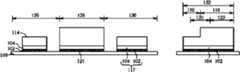
请参考图1,图1为本发明的液晶显示器的剖面结构示意图。如图1所示,基板100上至少概分成有四种区域,分别是薄膜晶体管区126、像素区128、电容区130和接触垫区132,其中薄膜晶体管区126、像素区128和电容区130会构成一像素单元。在本发明的丨较佳实施例中,设置在各像素单元内的薄膜晶体管区126上的薄膜晶体管结构均包含有一栅极115(其是由一透明导电层102和一第一金属层104所构成)、一绝缘层106、一半导体层108与由图案化的第二金属层110所形成的一源极与一漏极,和一保护层112。设置在各像素单元内的像素区128上的透明导电层102则与薄膜晶体管的漏极电性相连,用来当作像素电极121,并通过薄膜晶体管的栅极115开关来导入电压以驱动像素区128上方的液晶分子(未显示)。设置在各像素单元内的电容区130的金属电容(MIM capacitor),则具有一电容电极117(由透明导电层102和第一金属层104所构成),用以形成储存电容。而接触垫区132则是广设在基板100的周围,其内设置有堆栈的透明导电层102、第一金属层104与第二金属层110形成接触垫结构,用以对外交换讯号。Please refer to FIG. 1 , which is a schematic cross-sectional structure diagram of a liquid crystal display of the present invention. As shown in FIG. 1 , the
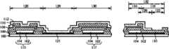
请参考图2至图13,图2至图13为本发明一种制作液晶显示器方法的步骤示意图。如图2所示,在本发明的丨较佳实施例中,首先提供一基板100。接着在基板100上依序全面沈积一透明导电层102和一第一金属层104。其中,基板100可为玻璃等的透明基板,透明导电层102可以为氧化铟锡(ITO)、氧化铟锌(IZO)或其它透明导电材质,第一金属层104可以为铝、钼、铬、钨、铜或上述金属的合金材料。此外,基板100上除了上述可概分成四种区域外(薄膜晶体管区126、像素区128、电容区130和接触垫区132),接触垫区132又可定义有一第一区域116、一第二区域118、一第三区域120和一第四区域122,第三区域120包含部分的第一区域116和部分的第二区域118,第四区域122则包含其余的第二区域118,第四区域122是作为后续接触垫结构的暴露区域。Please refer to FIG. 2 to FIG. 13 . FIG. 2 to FIG. 13 are schematic diagrams of steps of a method for manufacturing a liquid crystal display according to the present invention. As shown in FIG. 2, in a preferred embodiment of the present invention, a
接着,进行一第一光刻及刻蚀制造过程(photo-etching process,PEP)。首先,在基板100上全面形成一第一光致抗蚀剂膜114。接着利用一第一光掩膜(half tone mask)(未显示)进行一第一光刻制造过程,以在基板100上的各区域中形成不同厚度的图案化光致抗蚀剂。第一光掩膜可以是灰阶掩膜(gray tone mask)或是半色阶掩膜(half tone mask)等等。如图2所示,像素区128和接触垫区132的第二区域118所形成的第一光致抗蚀剂膜114最厚;而在薄膜晶体管区126中对应为栅极115的部位,和电容区130对应为电容电极117的部位,和接触垫区132的第一区域116,此三个区域为第一光掩膜的半穿透区,仅允许部分曝光光线通过,因此会形成次厚的第一光致抗蚀剂膜114;其余区域则在显影后,完全去除第一光致抗蚀剂膜114。Next, a first photolithography and etching process (photo-etching process, PEP) is performed. First, a first
接着如图3所示,利用不同厚度的图案化光致抗蚀剂膜114进行一第一刻蚀步骤,以移除未被第一光致抗蚀剂膜114覆盖的第一金属层104和透明导电层102。接着如图4所示,进行一第一灰化步骤,以非等向性缩减第一光致抗蚀剂膜114的厚度,也即将上述「次厚」的第一光致抗蚀剂膜114去除,也就是将薄膜晶体管区126的栅极115部位,和电容区130的电容电极117部位,和接触垫区132的第一区域116上方的第一光致抗蚀剂膜114去除,而分别在薄膜晶体管区126上留下图案化的透明导电层102与第一金属层104以形成栅极115结构,在像素区128上留下图案化的透明导电层102与第一金属层104,而在电容区130上留下图案化的透明导电层102与第一金属层104以形成电容电极117结构。由于像素区128和接触垫区132的第二区域118其上的第一光致抗蚀剂膜114较厚,因此在进行完第一灰化步骤后,此两区域上的第一光致抗蚀剂膜114还具有一定厚度的残留。Next, as shown in FIG. 3 , a first etching step is performed using patterned
接着请参考图5,在基板100上依序全面沈积一绝缘层106和一半导体层108。值得注意的是,由于在基板100上有第一光致抗蚀剂膜114,因此此一沈积步骤须以低温或室温的成膜制造过程进行。在本发明的较佳实施例中,半导体层108的材料是使用氧化铟锗锌(indiumgallium zinc oxide,IGZO),成膜的温度可在室温下进行,其包括一通入氧气和氩气的步骤,且氧气的体积百分比约为5%至10%。绝缘层108可为一单一(single)绝缘层或一复合(composite)绝缘层,其材质可包含有氧化硅(SiOx)、氮化硅(SiNy)或氮氧化硅(SiON)等。由于像素区128和第二区域118上还具有第一光致抗蚀剂膜114,因此形成在此两区的绝缘层106和半导体层108会覆盖在第一光致抗蚀剂膜114上。Next, referring to FIG. 5 , an
接着请参考图6,接着进行一第一去膜(lift-off)步骤以去除第一光致抗蚀剂膜114。例如以适当的清洗液去除位在像素区128和第二区域118所残留的第一光致抗蚀剂膜114,同时也一并去除覆盖在其上的绝缘层106和半导体层108。然后如图7所示,进行一刻蚀步骤以去除像素区128的第一金属层104以形成像素电极,和去除第二区域118的第一金属层104。Referring to FIG. 6 , a first lift-off step is performed to remove the first
如图8所示,在基板100上全面沈积一第二金属层110。接着进行一第二光刻及刻蚀制造过程,如图9所示。首先,沈积一第二光致抗蚀剂膜124,并利用一第二光掩膜(未显示)进行一第二光刻制造过程,以在基板100上的各区域中形成不同厚度的图案化光致抗蚀剂。第二光掩膜可以是灰阶掩膜(gray tone mask)或是半色阶掩膜(half tone mask)等等。如图9所示,第四区域122所形成的第二光致抗蚀剂膜124最厚;而在薄膜晶体管区126中对应为源极与漏极的区域,和电容区130和第三区域120仅允许部分的黄光穿透,因此会形成次厚的第二光致抗蚀剂膜124;而其余地区在显影后则无第二光致抗蚀剂膜124。As shown in FIG. 8 , a
随后如图10所示,进行一第二刻蚀步骤,移除未被第二光致抗蚀剂膜124覆盖的第二金属层110,使得在薄膜晶体管区126上留下图案化的第二金属层110而形成源极与漏极的结构。接着如图11所示,进行一第二灰化步骤,将上述「次厚」的第二光致抗蚀剂膜124去除,而仅留下位在第四区域122的第二光致抗蚀剂膜124。Subsequently, as shown in FIG. 10, a second etching step is performed to remove the
然后进行一沈积步骤,以在基板100上全面形成一保护层112,如图12所示,且位在第四区域122的保护层112会沈积在残留的第二光致抗蚀剂膜124上。保护层112可以为氧化硅、氮化硅或氮氧化硅等。A deposition step is then carried out to form a
之后进行一第二去膜步骤,如图13所示,以去除位在第四区域122的第二光致抗蚀剂膜124和其上的保护层112,并暴露出下方的第二金属层110。这些在各接触垫区132中所暴露出的第二金属层110则在基板100的边缘形成接触垫结构,用来与驱动集成电路(driving IC)或软性印刷电路版(Flexible Printed Circuit,FPC)等相电连接以对外提供讯号的输入和输出。最后再进行制备配向膜等的制造过程。A second film removal step is then performed, as shown in FIG. 13 , to remove the
由上述步骤,可以得到图1中本发明的薄膜晶体管的结构。特别的是,本发明所提供的薄膜晶体管,其作为栅极通道的半导体层108是由氧化铟锗锌所组成。主要的特点有二,第一是由于在本发明的制作方法中,是使用了去膜(lift-off)技术来减少光掩膜的使用次数,因此必须要在第一光致抗蚀剂膜114上形成半导体层108和绝缘层106,进而通过去膜光致抗蚀剂以同时图案化半导体层108与绝缘层106,因此半导体层108的沈积温度不能太高以破坏其下的第一光致抗蚀剂膜114,而氧化铟锗锌可在室温下形成,因此相当符合本制造过程和结构的需求。另外,在本发明的制造过程中,除了像素区128和第四区域122外,其余地区皆有覆盖半导体层108,因此考量到整体液晶显示器的透光率问题,半导体层108宜选用透光度高且无光漏电情况的材料,这也是本发明以氧化铟锗锌作为半导体层108材料的第二个原因。Through the above steps, the structure of the thin film transistor of the present invention in FIG. 1 can be obtained. In particular, in the thin film transistor provided by the present invention, the
综上而言,本发明所提出一种制作液晶显示器的方法,巧妙的运用了第一光掩膜、第二光掩膜和去膜制造过程,因此仅需要两道光掩膜即可完成现有技术中须以五道光掩膜的薄膜晶体管数组(TFT array),可大幅节省制造成本和污染微粒的影响,进而能有效提高良率与产能。另外,利用本发明的制作过程须考量到去膜制造过程的进行,和整体透光度的问题,本发明也提出了使用氧化铟锗锌作为半导体层的材料,适用在本发明制造过程中所制作的薄膜晶体管,可有效提升其使用品质。To sum up, the present invention proposes a method for manufacturing a liquid crystal display, which cleverly uses the first photomask, the second photomask and the film-removing manufacturing process, so only two photomasks are needed to complete the existing The technology requires a thin-film transistor array (TFT array) with five photomasks, which can greatly save manufacturing costs and the impact of contamination particles, thereby effectively improving yield and production capacity. In addition, the production process of the present invention must take into account the process of removing the film and the overall light transmittance. The present invention also proposes the use of indium germanium zinc oxide as the material of the semiconductor layer, which is suitable for the production process of the present invention. The manufactured thin film transistor can effectively improve its use quality.
以上所述仅为本发明的较佳实施例,凡依本发明申请专利范围所做的均等变化与修饰,皆应属本发明的涵盖范围。The above descriptions are only preferred embodiments of the present invention, and all equivalent changes and modifications made according to the scope of the patent application of the present invention shall fall within the scope of the present invention.
Claims (20)
Priority Applications (2)
| Application Number | Priority Date | Filing Date | Title |
|---|---|---|---|
| CN2009103080100ACN102033379B (en) | 2009-09-30 | 2009-09-30 | Liquid crystal display and manufacturing method thereof |
| US12/889,427US8431424B2 (en) | 2009-09-30 | 2010-09-24 | Liquid crystal display panel and fabrication method thereof |
Applications Claiming Priority (1)
| Application Number | Priority Date | Filing Date | Title |
|---|---|---|---|
| CN2009103080100ACN102033379B (en) | 2009-09-30 | 2009-09-30 | Liquid crystal display and manufacturing method thereof |
Publications (2)
| Publication Number | Publication Date |
|---|---|
| CN102033379A CN102033379A (en) | 2011-04-27 |
| CN102033379Btrue CN102033379B (en) | 2012-08-15 |
Family
ID=43779292
Family Applications (1)
| Application Number | Title | Priority Date | Filing Date |
|---|---|---|---|
| CN2009103080100AActiveCN102033379B (en) | 2009-09-30 | 2009-09-30 | Liquid crystal display and manufacturing method thereof |
Country Status (2)
| Country | Link |
|---|---|
| US (1) | US8431424B2 (en) |
| CN (1) | CN102033379B (en) |
Families Citing this family (9)
| Publication number | Priority date | Publication date | Assignee | Title |
|---|---|---|---|---|
| CN102033379B (en)* | 2009-09-30 | 2012-08-15 | 群康科技(深圳)有限公司 | Liquid crystal display and manufacturing method thereof |
| EP2492780B1 (en)* | 2009-11-26 | 2014-07-02 | Sharp Kabushiki Kaisha | A touch panel manufacturing method, and a method for manufacturing a display device provided with a touch panel |
| KR101780250B1 (en)* | 2010-09-24 | 2017-09-22 | 삼성디스플레이 주식회사 | Organinc light emitting display device and manufacturing method for the same |
| TWI459255B (en)* | 2011-08-04 | 2014-11-01 | Innolux Corp | Touch panel, touch display apparatus using the same and manufacturing method thereof |
| CN103280429B (en)* | 2012-12-21 | 2015-02-11 | 上海中航光电子有限公司 | Manufacturing method of thin film transistor (TFT) array substrate and TFT array substrate |
| US20140197519A1 (en)* | 2013-01-17 | 2014-07-17 | Qualcomm Incorporated | Mim capacitor and mim capacitor fabrication for semiconductor devices |
| CN103227148B (en)* | 2013-04-02 | 2015-12-23 | 京东方科技集团股份有限公司 | A kind of array base palte preparation method and array base palte and display unit |
| CN113013096B (en) | 2021-03-01 | 2023-06-02 | 重庆先进光电显示技术研究院 | Preparation method of array substrate and array substrate |
| CN113178493A (en)* | 2021-04-25 | 2021-07-27 | 京东方科技集团股份有限公司 | Thin film transistor, preparation method and display panel |
Citations (2)
| Publication number | Priority date | Publication date | Assignee | Title |
|---|---|---|---|---|
| CN101025536A (en)* | 2006-02-24 | 2007-08-29 | 株式会社日立显示器 | Liquid crystal display device |
| CN101335304A (en)* | 2005-09-29 | 2008-12-31 | 株式会社半导体能源研究所 | Semiconductor device and manufacturing method thereof |
Family Cites Families (21)
| Publication number | Priority date | Publication date | Assignee | Title |
|---|---|---|---|---|
| KR100399291B1 (en)* | 1997-01-27 | 2004-01-24 | 가부시키가이샤 아드반스트 디스프레이 | Liquid crystal display device using semiconductor thin film transistor, manufacturing method thereof, semiconductor thin film transistor array substrate and corresponding semiconductor thin film transistor array substrate |
| KR100309209B1 (en)* | 1999-07-31 | 2001-09-29 | 구본준, 론 위라하디락사 | Liquid crystal display and method for fabricating the same |
| KR100582599B1 (en)* | 1999-10-25 | 2006-05-23 | 엘지.필립스 엘시디 주식회사 | Liquid crystal display device manufacturing method and liquid crystal display device according to the manufacturing method |
| KR100654158B1 (en)* | 1999-10-25 | 2006-12-05 | 엘지.필립스 엘시디 주식회사 | Liquid crystal display device manufacturing method and liquid crystal display device according to the manufacturing method |
| JP4035094B2 (en)* | 2002-07-31 | 2008-01-16 | エルジー.フィリップス エルシーデー カンパニー,リミテッド | Reflective transmission type liquid crystal display device and manufacturing method thereof |
| US7279370B2 (en)* | 2003-10-11 | 2007-10-09 | Lg.Philips Lcd Co., Ltd. | Thin film transistor array substrate and method of fabricating the same |
| US6869833B1 (en)* | 2004-03-16 | 2005-03-22 | Quanta Display Inc. | Method of manufacturing a thin film transistor of a liquid crystal display |
| KR101197223B1 (en)* | 2005-09-09 | 2012-11-02 | 엘지디스플레이 주식회사 | An array substrate for trans-flective liquid crystal display device and fabrication method of the same |
| KR101202983B1 (en)* | 2005-09-13 | 2012-11-20 | 엘지디스플레이 주식회사 | An array substrate for trans-flective liquid crystal display device and fabrication method of the same |
| KR100729043B1 (en)* | 2005-09-14 | 2007-06-14 | 삼성에스디아이 주식회사 | Transparent thin film transistor and method for manufacturing same |
| KR101151799B1 (en)* | 2005-11-09 | 2012-06-01 | 엘지디스플레이 주식회사 | An array substrate of LCD and Method of fabricating of the same |
| KR101221261B1 (en)* | 2006-02-15 | 2013-01-11 | 엘지디스플레이 주식회사 | Array substrate for LCD and the fabrication method thereof |
| US7988871B2 (en)* | 2007-07-20 | 2011-08-02 | Lg Display Co., Ltd. | Method of lifting off and fabricating array substrate for liquid crystal display device using the same |
| CN101840922B (en)* | 2009-03-16 | 2012-05-30 | 北京京东方光电科技有限公司 | Array substrate and manufacturing method |
| KR101213708B1 (en)* | 2009-06-03 | 2012-12-18 | 엘지디스플레이 주식회사 | Array substrate and method of fabricating the same |
| CN101957529B (en)* | 2009-07-16 | 2013-02-13 | 北京京东方光电科技有限公司 | FFS (Fringe Field Switching) type TFT-LCD (Thin Film Transistor Liquid Crystal Display) array substrate and manufacturing method thereof |
| CN101995708B (en)* | 2009-08-19 | 2013-04-03 | 北京京东方光电科技有限公司 | TFT-LCD array substrate and manufacturing method thereof |
| CN102033379B (en)* | 2009-09-30 | 2012-08-15 | 群康科技(深圳)有限公司 | Liquid crystal display and manufacturing method thereof |
| TW201128473A (en)* | 2010-02-09 | 2011-08-16 | Novatek Microelectronics Corp | Touch detection method and touch detection device and touch display device |
| CN102148195B (en)* | 2010-04-26 | 2013-05-01 | 北京京东方光电科技有限公司 | TFT-LCD (thin film transistor-liquid crystal display) array substrate and manufacturing method thereof |
| KR101790176B1 (en)* | 2010-11-02 | 2017-10-25 | 엘지디스플레이 주식회사 | Method of fabricating array substrate |
- 2009
- 2009-09-30CNCN2009103080100Apatent/CN102033379B/enactiveActive
- 2010
- 2010-09-24USUS12/889,427patent/US8431424B2/enactiveActive
Patent Citations (2)
| Publication number | Priority date | Publication date | Assignee | Title |
|---|---|---|---|---|
| CN101335304A (en)* | 2005-09-29 | 2008-12-31 | 株式会社半导体能源研究所 | Semiconductor device and manufacturing method thereof |
| CN101025536A (en)* | 2006-02-24 | 2007-08-29 | 株式会社日立显示器 | Liquid crystal display device |
Also Published As
| Publication number | Publication date |
|---|---|
| CN102033379A (en) | 2011-04-27 |
| US20110073855A1 (en) | 2011-03-31 |
| US8431424B2 (en) | 2013-04-30 |
Similar Documents
| Publication | Publication Date | Title |
|---|---|---|
| CN102033379B (en) | Liquid crystal display and manufacturing method thereof | |
| CN102270604B (en) | Structure of array substrate and manufacturing method thereof | |
| CN101957530A (en) | TFT-LCD (Thin Film Transistor-Liquid Crystal Display) array baseplate and manufacturing method thereof | |
| CN103178119B (en) | Array base palte, array base palte preparation method and display unit | |
| CN104201152A (en) | Method for manufacturing display panel | |
| CN105957867B (en) | Array substrate motherboard and preparation method thereof, display device | |
| CN102629585A (en) | Display device, thin film transistor, array substrate and manufacturing method thereof | |
| TWI298545B (en) | Method for fabricating a thin film transistor | |
| CN106847836B (en) | TFT substrate and manufacturing method thereof | |
| CN103309105B (en) | Array base palte and preparation method thereof, display device | |
| US9502437B2 (en) | Method of manufacturing array substrate, array substrate and display device | |
| CN105655359A (en) | Method for manufacturing TFT (thin-film transistor) substrates | |
| CN104392990B (en) | A kind of array substrate and display device | |
| CN104835782A (en) | Array substrate, manufacturing method of array substrate and display device | |
| US9219088B2 (en) | Array substrate, manufacturing method thereof, and display device | |
| WO2013026375A1 (en) | Thin film transistor array substrate and its manufacturing method and an electronic device | |
| CN104076567A (en) | Array substrate, manufacturing method of array substrate and display device | |
| CN105679714A (en) | Array substrate and manufacturing method therefor | |
| CN102654703A (en) | Array substrate and manufacturing method thereof as well as display equipment | |
| CN103048840B (en) | Array substrate, manufacture method of array substrate, liquid crystal display panel and display device | |
| CN103117248A (en) | Array substrate and manufacture method thereof and display device | |
| CN105552028A (en) | Array substrate, fabrication method thereof, display panel and display device | |
| CN105070765A (en) | Thin film transistor, array substrate, display device and manufacturing method | |
| WO2020093442A1 (en) | Method for manufacturing array substrate, and array substrate | |
| CN101150093B (en) | Method for manufacturing pixel structure |
Legal Events
| Date | Code | Title | Description |
|---|---|---|---|
| C06 | Publication | ||
| PB01 | Publication | ||
| C10 | Entry into substantive examination | ||
| SE01 | Entry into force of request for substantive examination | ||
| C53 | Correction of patent of invention or patent application | ||
| CB02 | Change of applicant information | Address after:518109 Longhua, Shenzhen, town, Foxconn science and Technology Industrial Park E District, building 1, floor 4, Applicant after:Qunkang Technology (Shenzhen) Co., Ltd. Co-applicant after:Chimei Optoelectronics Co., Ltd. Address before:518109 Longhua, Shenzhen, town, Foxconn science and Technology Industrial Park E District, building 1, floor 4, Applicant before:Qunkang Technology (Shenzhen) Co., Ltd. Co-applicant before:Innolux Display Group | |
| C14 | Grant of patent or utility model | ||
| GR01 | Patent grant |