CN102023440A - Structure of touch screen and manufacturing method thereof - Google Patents
Structure of touch screen and manufacturing method thereofDownload PDFInfo
- Publication number
- CN102023440A CN102023440ACN2009103070378ACN200910307037ACN102023440ACN 102023440 ACN102023440 ACN 102023440ACN 2009103070378 ACN2009103070378 ACN 2009103070378ACN 200910307037 ACN200910307037 ACN 200910307037ACN 102023440 ACN102023440 ACN 102023440A
- Authority
- CN
- China
- Prior art keywords
- electrode
- substrate
- touch screen
- electrically connected
- auxiliary
- Prior art date
- Legal status (The legal status is an assumption and is not a legal conclusion. Google has not performed a legal analysis and makes no representation as to the accuracy of the status listed.)
- Granted
Links
Images


Classifications
- G—PHYSICS
- G06—COMPUTING OR CALCULATING; COUNTING
- G06F—ELECTRIC DIGITAL DATA PROCESSING
- G06F3/00—Input arrangements for transferring data to be processed into a form capable of being handled by the computer; Output arrangements for transferring data from processing unit to output unit, e.g. interface arrangements
- G06F3/01—Input arrangements or combined input and output arrangements for interaction between user and computer
- G06F3/03—Arrangements for converting the position or the displacement of a member into a coded form
- G06F3/041—Digitisers, e.g. for touch screens or touch pads, characterised by the transducing means
- G06F3/0412—Digitisers structurally integrated in a display
- G—PHYSICS
- G06—COMPUTING OR CALCULATING; COUNTING
- G06F—ELECTRIC DIGITAL DATA PROCESSING
- G06F3/00—Input arrangements for transferring data to be processed into a form capable of being handled by the computer; Output arrangements for transferring data from processing unit to output unit, e.g. interface arrangements
- G06F3/01—Input arrangements or combined input and output arrangements for interaction between user and computer
- G06F3/03—Arrangements for converting the position or the displacement of a member into a coded form
- G06F3/041—Digitisers, e.g. for touch screens or touch pads, characterised by the transducing means
- G06F3/044—Digitisers, e.g. for touch screens or touch pads, characterised by the transducing means by capacitive means
- G06F3/0445—Digitisers, e.g. for touch screens or touch pads, characterised by the transducing means by capacitive means using two or more layers of sensing electrodes, e.g. using two layers of electrodes separated by a dielectric layer
- G—PHYSICS
- G06—COMPUTING OR CALCULATING; COUNTING
- G06F—ELECTRIC DIGITAL DATA PROCESSING
- G06F3/00—Input arrangements for transferring data to be processed into a form capable of being handled by the computer; Output arrangements for transferring data from processing unit to output unit, e.g. interface arrangements
- G06F3/01—Input arrangements or combined input and output arrangements for interaction between user and computer
- G06F3/03—Arrangements for converting the position or the displacement of a member into a coded form
- G06F3/041—Digitisers, e.g. for touch screens or touch pads, characterised by the transducing means
- G06F3/044—Digitisers, e.g. for touch screens or touch pads, characterised by the transducing means by capacitive means
- G06F3/0448—Details of the electrode shape, e.g. for enhancing the detection of touches, for generating specific electric field shapes, for enhancing display quality
- H—ELECTRICITY
- H10—SEMICONDUCTOR DEVICES; ELECTRIC SOLID-STATE DEVICES NOT OTHERWISE PROVIDED FOR
- H10D—INORGANIC ELECTRIC SEMICONDUCTOR DEVICES
- H10D86/00—Integrated devices formed in or on insulating or conducting substrates, e.g. formed in silicon-on-insulator [SOI] substrates or on stainless steel or glass substrates
- H10D86/40—Integrated devices formed in or on insulating or conducting substrates, e.g. formed in silicon-on-insulator [SOI] substrates or on stainless steel or glass substrates characterised by multiple TFTs
- H10D86/481—Integrated devices formed in or on insulating or conducting substrates, e.g. formed in silicon-on-insulator [SOI] substrates or on stainless steel or glass substrates characterised by multiple TFTs integrated with passive devices, e.g. auxiliary capacitors
- H—ELECTRICITY
- H10—SEMICONDUCTOR DEVICES; ELECTRIC SOLID-STATE DEVICES NOT OTHERWISE PROVIDED FOR
- H10D—INORGANIC ELECTRIC SEMICONDUCTOR DEVICES
- H10D86/00—Integrated devices formed in or on insulating or conducting substrates, e.g. formed in silicon-on-insulator [SOI] substrates or on stainless steel or glass substrates
- H10D86/40—Integrated devices formed in or on insulating or conducting substrates, e.g. formed in silicon-on-insulator [SOI] substrates or on stainless steel or glass substrates characterised by multiple TFTs
- H10D86/60—Integrated devices formed in or on insulating or conducting substrates, e.g. formed in silicon-on-insulator [SOI] substrates or on stainless steel or glass substrates characterised by multiple TFTs wherein the TFTs are in active matrices
- H—ELECTRICITY
- H10—SEMICONDUCTOR DEVICES; ELECTRIC SOLID-STATE DEVICES NOT OTHERWISE PROVIDED FOR
- H10D—INORGANIC ELECTRIC SEMICONDUCTOR DEVICES
- H10D86/00—Integrated devices formed in or on insulating or conducting substrates, e.g. formed in silicon-on-insulator [SOI] substrates or on stainless steel or glass substrates
- H10D86/80—Integrated devices formed in or on insulating or conducting substrates, e.g. formed in silicon-on-insulator [SOI] substrates or on stainless steel or glass substrates characterised by multiple passive components, e.g. resistors, capacitors or inductors
Landscapes
- Engineering & Computer Science (AREA)
- General Engineering & Computer Science (AREA)
- Theoretical Computer Science (AREA)
- Human Computer Interaction (AREA)
- Physics & Mathematics (AREA)
- General Physics & Mathematics (AREA)
- Quality & Reliability (AREA)
- Position Input By Displaying (AREA)
- Liquid Crystal (AREA)
- Thin Film Transistor (AREA)
- Devices For Indicating Variable Information By Combining Individual Elements (AREA)
Abstract
Translated fromChinese
Description
Translated fromChinese技术领域technical field
本发明涉及一种触控装置,尤其是指一种触控屏幕的结构及其制造方法。The present invention relates to a touch device, in particular to a structure of a touch screen and a manufacturing method thereof.
背景技术Background technique
在现今各式消费性电子产品市场中,个人数字助理(personal digital assistant,PDA)、行动电话(mobile Phone)及笔记型计算机(notebook)等可携式电子产品乃至于个人计算机、数字家电系统皆已逐渐使用触控屏幕(touch display panel)作为使用者与电子装置间的数据沟通接口工具。使用触控屏幕时,使用者可以直接透过屏幕上显示的对象进行操作与下达指令,提供使用者更人性化的操作接口。此外电子产品的设计皆以轻、薄、短、小是方向,因此在产品设计上希望能节省如按键、键盘、鼠标等传统输入装置的设置空间,因此搭配触控式屏幕的显示装置已逐渐成为各式电子产品的关键零组件之一。In today's market of various consumer electronics products, portable electronic products such as personal digital assistant (PDA), mobile phone (mobile Phone) and notebook computer (notebook), as well as personal computers and digital home appliance systems are all A touch display panel has been gradually used as a data communication interface tool between the user and the electronic device. When using the touch screen, the user can directly operate and issue instructions through the objects displayed on the screen, providing the user with a more humanized operation interface. In addition, the design of electronic products is light, thin, short, and small. Therefore, in product design, it is hoped to save the installation space of traditional input devices such as buttons, keyboards, and mice. Therefore, display devices with touch screens have gradually Become one of the key components of various electronic products.
触控屏幕依据其结构,可以分为外加式触控屏幕以及内嵌式触控屏幕。外加式触控屏幕除了一显示面板外,还需外加一独立的触控面板在显示面板上,因此使用者在观看显示面板所呈现的影像时,可以通过触控面板来感测其触控位置。而内嵌式触控屏幕,则整合了触控功能于现有的显示面板内,因此同一面板即同时具有输入与传输的功能,其操作接口较外加式触控屏幕更为直觉。另一方面,由于无需额外的触控层,故与外加式触控屏幕相比,内嵌式触控屏幕具有更好的显示品质以及较低的耗电量,且更为轻薄短小,是目前触控屏幕的发展趋势。According to its structure, touch screens can be divided into external touch screens and built-in touch screens. In addition to a display panel, the external touch screen also needs to add an independent touch panel on the display panel, so when the user watches the image presented by the display panel, he can sense the touch position through the touch panel . The built-in touch screen integrates the touch function into the existing display panel, so the same panel has the functions of input and transmission at the same time, and its operation interface is more intuitive than that of the external touch screen. On the other hand, since no additional touch layer is required, compared with the external touch screen, the built-in touch screen has better display quality and lower power consumption, and is thinner, lighter and shorter. The development trend of touch screen.
现有的内嵌式触控屏幕技术是将一感测组件,如光感测组件,整合至薄膜晶体管(TFT)阵列中,也就是将一光感测组件与现有的薄膜晶体管整合于同一个像素内,并通过不同的驱动讯号以及侦测讯号,以在同一个像素之中同时达到显示以及侦测触控的效果。一般光感测组件的原理是利用半导体材料例如非晶硅(amorphous silicon)在照光之后会产生光电荷的特性,通过侦测其光电流的产生来侦测其触控位置。现有的光感测组件包括非晶硅薄膜晶体管(amorphous silicon TFT)或者是PIN光二极管(p-intrinsic-n photodiode),两者都可以成功整合于现有的液晶显示面板中,但也存在着若干缺点。例如,以非晶硅薄膜晶体管作为光感测组件的结构时,由于长时间暴露于光线下,其非晶硅材料的光电效应会逐渐衰退而使得感光能力逐渐丧失。而若以PIN光二极管作为光感测组件时,由于多晶硅的吸光效率不佳,且在现有架构下,无法增加多晶硅的厚度来改善其光敏感度,因此在光线不充足的环境下,其侦测敏感度并不理想。The existing in-cell touch screen technology is to integrate a sensing element, such as a light sensing element, into a thin film transistor (TFT) array, that is, to integrate a light sensing element and an existing thin film transistor into the same In one pixel, different driving signals and detection signals are used to simultaneously achieve display and touch detection effects in the same pixel. The principle of the general photo-sensing element is to use the characteristics of semiconductor materials such as amorphous silicon (amorphous silicon) to generate photo-charges after being irradiated with light, and detect the touch position by detecting the generation of photo-current. Existing light sensing components include amorphous silicon thin film transistor (amorphous silicon TFT) or PIN photodiode (p-intrinsic-n photodiode), both of which can be successfully integrated into existing liquid crystal display panels, but there are also There are several disadvantages. For example, when an amorphous silicon thin film transistor is used as the structure of the photo-sensing component, due to long-time exposure to light, the photoelectric effect of the amorphous silicon material will gradually decline and the light-sensing ability will be gradually lost. However, if a PIN photodiode is used as a light-sensing component, due to the poor light absorption efficiency of polysilicon, and under the existing structure, it is impossible to increase the thickness of polysilicon to improve its light sensitivity. Sensitivity is not ideal.
发明内容Contents of the invention
为解决现有触控屏幕组件衰退与组件灵敏度的问题,本发明提供一种可有效避免组件衰退和灵敏度好的触控屏幕的结构,以及一种触控屏幕结构的制造方法。In order to solve the problem of component degradation and component sensitivity of the existing touch screen, the present invention provides a touch screen structure that can effectively avoid component degradation and has good sensitivity, and a manufacturing method of the touch screen structure.
一种触控屏幕的结构,包括一基板、多条扫描线、多条数据线、多条数据传输线、多个薄膜晶体管以及多个侦测电容皆设置于基板上。各数据线与各扫描线于基板上划分出多个呈阵列排列的像素区域。每条数据传输线设置于每条数据线旁。各薄膜晶体管电性连接至其所对应的扫描线与数据线;而各侦测电容电性连接至所对应的扫描线与数据传输线。A touch screen structure includes a substrate, multiple scanning lines, multiple data lines, multiple data transmission lines, multiple thin film transistors and multiple detection capacitors all arranged on the substrate. Each data line and each scan line divides a plurality of pixel areas arranged in an array on the substrate. Each data transmission line is arranged beside each data line. Each thin film transistor is electrically connected to its corresponding scan line and data line; and each detection capacitor is electrically connected to its corresponding scan line and data transmission line.
一种触控屏幕结构的制造方法,包括提供一基板,并在基板上形成一栅极、一辅助栅极以及一第一电极,接着在基板上形成一介电层,覆盖在栅极、辅助栅极以及第一电极上;然后在栅极上的介电层上行成一通道层,在辅助栅极上的介电层上形成一辅助通道层,同时在第一电极上的介电层上形成一第二电极。在通道层上形成一源极与一漏极,在辅助通道层上形成一辅助源极与一辅助漏极,其中辅助源极与第二电极电性连接,并部份覆盖该第二电极。最后在基板上形成一保护层,以覆盖源极、漏极、辅助源极、辅助漏极以及第二电极。A method for manufacturing a touch screen structure, comprising providing a substrate, and forming a grid, an auxiliary grid, and a first electrode on the substrate, and then forming a dielectric layer on the substrate, covering the grid, the auxiliary On the gate and the first electrode; then form a channel layer on the dielectric layer on the gate, form an auxiliary channel layer on the dielectric layer on the auxiliary gate, and form an auxiliary channel layer on the dielectric layer on the first electrode at the same time a second electrode. A source and a drain are formed on the channel layer, and an auxiliary source and an auxiliary drain are formed on the auxiliary channel layer, wherein the auxiliary source is electrically connected to the second electrode and partially covers the second electrode. Finally, a protection layer is formed on the substrate to cover the source, the drain, the auxiliary source, the auxiliary drain and the second electrode.
本发明提供了一种内嵌式触控屏幕的结构与结构的制造方法,其是在现有的薄膜晶体管阵列中,嵌入了一非晶硅电容结构,利用环境光照射使得非晶硅层所产生的电荷变化而造成电容值的改变,完成触控面板的操作。非晶硅电容结构可以改善现有技术中组件衰退以及灵敏度不足的问题。The present invention provides a structure and a manufacturing method of an embedded touch screen, which is to embed an amorphous silicon capacitor structure in the existing thin film transistor array, and utilize ambient light to make the amorphous silicon layer The generated charge changes to cause a change in the capacitance value to complete the operation of the touch panel. The amorphous silicon capacitor structure can improve the problems of component degradation and insufficient sensitivity in the prior art.
附图说明Description of drawings
图1是本发明的较佳实施例的触控式屏幕结构的等效电路示意图。FIG. 1 is a schematic diagram of an equivalent circuit of a touch screen structure according to a preferred embodiment of the present invention.
图2至图6是本发明的较佳实施例的触控式屏幕结构的制造方法示意图。2 to 6 are schematic diagrams of the manufacturing method of the touch screen structure according to the preferred embodiment of the present invention.
图7是本发明的较佳实施例中的侦测电容的仰视图。FIG. 7 is a bottom view of the detection capacitor in a preferred embodiment of the present invention.
图8是本发明的较佳实施例中的侦测电容达到多点触控的示意图。FIG. 8 is a schematic diagram of detecting capacitance to achieve multi-touch in a preferred embodiment of the present invention.
图9是本发明的较佳实施例中的侦测电容的结构示意图。FIG. 9 is a schematic structural diagram of a detection capacitor in a preferred embodiment of the present invention.
图10至图13是本发明的较佳实施例中的侦测电容的制造方法示意图。10 to 13 are schematic diagrams of the manufacturing method of the detection capacitor in a preferred embodiment of the present invention.
具体实施方式Detailed ways
请参阅图1和图6,图1是本发明的一实施例中一种触控式屏幕结构的等效电路示意图,图6则是其结构剖面示意图。如图1所示,触控屏幕结构的基板上配置有多条水平以及垂直交错的扫描线(gate line,GL)100、数据线(data line,DL)102以及数据传输线(outputline,OL)119。每两条相邻的扫描线100以及两条相邻的数据线102所包围的区域则是单一像素,每条数据传输线119则设置于每条数据线102旁,并实质上与各数据线102平行。每个像素内则具有一薄膜晶体管104以及一储存电容106。由图1和图6可以得知,薄膜晶体管104具有一与扫描线100电连接的栅极112,一与数据线102电连接的源极124和一与一像素电极136电性连接的漏极126。存储电容106则具有一与共享配线(未显示)电性连接的存储下电极144,还具有一与像素电极136电性连接的存储上电极128。因此,通过施以适当电压于扫描线100上便可以开启栅极112,数据线102的讯号即可以通过薄膜晶体管104而导通于像素电极136,进而驱动位于像素区域的液晶分子(未显示),以改变光线的偏振状态,而达成显示的效果,并可以通过存储电容106进行电位的储存,以维持像素电极136的驱动效果。值得注意的是,为了能够达成内嵌式触控屏幕结构侦测的效果,本发明的实施例在基板上还具有一侦测电容108。本发明的实施例可以在每固定数量个的像素中设置一侦测电容108,例如每2乘2的像素区域内即固定设置有一侦测电容108;当然,也可以每个像素中皆设置有一侦测电容108,视不同产品的侦测密度考量而做调整。请参考图1和图6,侦测电容108的结构由下而上是一第一电极116、一介电层118、一第二电极122以及一传输电极130。第一电极116会电连接至扫描线100,而第二电极122则会电性连接至数据传输线119。第一电极116是一金属导电层,其材料可以是铜、铝或其它导电材料。介电层118可以是一单一(single)绝缘层或一复合(composite)绝缘层,其材料可以包括有氧化硅(SiOx)、氮化硅(SiNy)或氮氧化硅(SiON)等。第二电极122具有一半导体层以及一重掺杂半导体层,其材料例如是一含氢的非晶硅层(amorphous silicon)。而传输电极130和第一电极116同样可以是金属的导电层。通过两电极以及位于其中的介电层118,即可以形成一电容结构,请参考图7,其是本发明的一实施例的侦测电容仰视图。如图7所示,第一电极116与第二电极122是电容结构中的两导电电极,中间以介电层118隔开(图7中未显示介电层118)。两电极重叠的形状以及大小可以视产品需求而做调整。例如重叠的形状是圆形、矩形或是不规则形状等。重叠的面积大小会影响侦测电容108在照光时与不照光时,其电容差异的变化值。因此,通过适当设计两电极重叠面积或是形状,可以使侦测电容108照光时的电容值与不照光时的电容值,有着明显的差异,从而增加其感光灵敏度。另外,其第二电极122所感应的电容变化值透过传输电极130而连接至数据传输线119。为了避免数据传输线119通过传输电极130而和第一电极116产生寄生电容而影响侦测电容108的准确性,因此在设计上,传输电极130与第一电极116应避免上下过多部分的重叠,例如图7中,传输电极130仅接触第二电极122的一侧部,使得传输电极130仅有小部分重叠于第一电极116上。本发明的侦测电容108的原理同样也是利用第二电极122中的半导体材质(非晶硅)会吸收光子而产生光电效应来感测。例如,在一外部亮光的环境下触碰此像素区域时,其手指按压处会遮住外光,因此侦测电容108的第二电极122的非晶硅并没有被光激发而产生光电效应,侦测电容108上的电容值维持不变;而设在触控式屏幕结构上未被手指触碰处的侦测电容108,其侦测电容108的非晶硅材料便会因光照而产生光电荷,并累积在非晶硅材料的表面,导致这些未被手指触碰与遮蔽的侦测电容108的电容值改变,然后再利用相对应的数据传输线119即可以用来侦测其电容改变值。因此,通过一讯号处理器(未显示)来接受各数据传输线119所传递的电容差异值,即可以运算而得知手指触碰的位置所在。反之,若在外部环境是暗处时,其是利用显示面板的背光模组(backlightmodule)提供光源,而在手指触碰处,光线会经由手指反射而进入触碰区的像素内,使得相对应的该等侦测电容108的非晶硅因光电效应而产生电容值的变化,而在其它没有被手指触碰的地方,其侦测电容108则不会有电容值的改变。同样的,通过各数据传输线119所传输的电容值,即可以得知暗处时手指的触碰位置。由上述操作方式可以得知,侦测电容108可以透过明暗处两种不同模式的侦测方式,利用一讯号处理器处理各数据传输线119所传递电容变化值的讯息,即可以得知其触碰位置。Please refer to FIG. 1 and FIG. 6 . FIG. 1 is a schematic diagram of an equivalent circuit of a touch screen structure according to an embodiment of the present invention, and FIG. 6 is a schematic cross-sectional diagram of the structure. As shown in FIG. 1 , a plurality of horizontal and vertical staggered scanning lines (gate line, GL) 100, data lines (data line, DL) 102 and data transmission lines (output line, OL) 119 are arranged on the substrate of the touch screen structure. . The area surrounded by every two
值得注意的是,第一电极116除了作为电容电极外,还可以挡住下方来自背光模组(未显示)的光线,可以避免在正常的情况下,其第二电极122的半导体材料直接受到背光模组光源的照射而干扰其光侦测能力。在现有技术中,还需要形成额外的遮光物才能达成这样的效果,而侦测电容108的设计则整合了此遮光效果,可以省却额外形成遮光物的步骤。It should be noted that, in addition to being a capacitive electrode, the
本发明的侦测电容108也可以感知多点触碰,请参考图8。当手指触碰在触控屏幕结构上同一行的像素时,例如同时触碰A、B两处,扫描线GL1进行扫描时同时驱动此行的侦测电容108,而触碰点A、B两处的电容值因手指的触碰而发生改变,其电容变化值则分别通过数据传输线OL2以及OL5传输,并通过一讯号处理器(未显示)即可以感知其触碰位置。而当手指触碰在触控屏幕结构上同一列的像素时,例如同时触碰A、C两处,在扫描线GL1开启时,数据传输线OL2会感知一电容变化值,而随着扫描线依序往下扫描,当扫描至GL4时,数据传输线OL2也会感知一电容变化值,因此通过不同的扫描时间点,虽然同一列的像素共享同一数据传输线,但在讯号处理器在不同时间点接受讯息的情况下,仍可以感知多点触碰的位置。The
本发明的实施例的侦测电容除了上述优点外,还可以完全整合于现有制造薄膜晶体管阵列的制程。请参考图2至图6,是本实施例中一种制造触控式屏幕结构的方法示意图,其是通过常用的五道光掩模制程,其中每一张图即代表着一道光掩模步骤。请先参考图2,首先在一基板110上沉积一第一金属层(未显示),接着利用第一道光掩模来图案化第一金属层,以分别形成扫描线(未显示)、薄膜晶体管104的一栅极112、存储电容106的一存储下电极144以及侦测电容108的一第一电极116。In addition to the above-mentioned advantages, the detection capacitor of the embodiment of the present invention can also be fully integrated into the existing manufacturing process of the thin film transistor array. Please refer to FIG. 2 to FIG. 6 , which are schematic diagrams of a method for manufacturing a touch screen structure in this embodiment, which uses a commonly used five-step photomask process, wherein each figure represents a photomask step. Please refer to FIG. 2 first. First, a first metal layer (not shown) is deposited on a
接着如图3所示,在基板110上全面沉积一介电层118,用来当作栅极绝缘层,其覆盖在栅极112、存储下电极144以及第一电极116上。接着沉积一半导体层以及一重掺杂半导体层(未显示),然后以第二道光掩模来图案化半导体层以及重掺杂半导体层,以形成薄膜晶体管104的信道层120以及侦测电容108的一第二电极122。因此可以理解的是,侦测电容108的第二电极122会包括一半导体层以及一重掺杂半导体层。Next, as shown in FIG. 3 , a
接着如图4所示,在基板110上全面沉积一第二金属层(未显示),并利用第三道光掩模来图案化此第二金属层,以形成数据线(未显示)、薄膜晶体管104的一源极124以及一漏极126、存储电容106的存储上电极128、数据传输线(未显示)以及侦测电容108的传输电极130,其中传输电极130会覆盖在第二电极122上方,与第二电极122有部分重叠,形成耦接,而另一端则会电连接于数据传输线119。Next, as shown in FIG. 4 , a second metal layer (not shown) is deposited on the entire surface of the
接着如图5所示,在基板110上全面沉积一保护层132,并利用第四道光掩模来图案化保护层,以在漏极126上方的保护层132中形成一接触洞134,同样的也在存储电容106的存储上电极128的上方形成另一接触洞134,以作为后续透明薄膜层电连接的通孔。Next, as shown in FIG. 5, a
接着请参考图6,在基板110上全面形成一透明导电层(未显示),然后以第五道光掩模图案化透明导电层,以形成一像素电极136。像素电极136会填入接触洞134,以电性连接漏极126以及存储上电极128。Next, please refer to FIG. 6 , a transparent conductive layer (not shown) is formed on the entire surface of the
通过上面步骤,即可以在现有五道光掩模的步骤下,在基板110上形成薄膜晶体管104、存储电容106以及侦测电容108,因此可以完全兼容于业界现有的薄膜晶体管制程,而不需作额外的设计与改良。Through the above steps, the
接着请参考图9,是本发明的一实施例的侦测电容结构的示意图。如图9所示,侦测电容108也可以透过另一辅助晶体管109来驱动,并以相对应的数据线102作为讯号传输端。侦测电容108的第一电极116是连接像素内的共通线(未显示),而第二电极122则连接至辅助晶体管109,透过侦测扫描线(SL)103作为此辅助晶体管109的开关,得以把电容变化值的讯号传递至相对应的数据线102作为讯号传输。在此实施方式中,由于是和同一个像素中的薄膜晶体管104共享数据线102,因此为了避免讯号的干扰,其扫描线100与侦测扫描线103的扫描必须交错实施,例如扫描线100先依序由上至下扫描时,此时的数据线102用作薄膜晶体管104的讯号输入端,使得薄膜晶体管104能根据不同数据线102的讯号而达到显示的效果。而当扫描线100由上而下扫描结束后,接着换侦测扫描线103依序由上而下扫描,并依序开通其对应的辅助晶体管109,此时的数据线102则作为侦测电容108的数据传输端,使侦测电容108上的电容值透过数据线102而进行传输,如此一来,通过不同的扫描时间,数据线102可以作为薄膜晶体管104的讯号输入端及侦测电容108的侦测传输端。Next, please refer to FIG. 9 , which is a schematic diagram of a detection capacitor structure according to an embodiment of the present invention. As shown in FIG. 9 , the
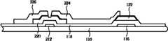
关于上述辅助晶体管109与侦测电容108的制造方式,请参考图10至图13,是本发明的一实施例中的侦测电容结构的制造方法示意图。请参考图10,首先在一基板110上沉积一第一金属层(未显示),接着利用第一道光掩模来图案化第一金属层,以分别形成扫描线(未显示)、侦测扫描线(未显示)、辅助晶体管109的一栅极212、存储电容106的存储下电极(未显示)以及侦测电容108的一第一电极116。Regarding the manufacturing method of the
接着如图11所示,在基板110上全面沉积一介电层118,用来当作栅极绝缘层,并覆盖在辅助晶体管的栅极212以及第一电极116上。接着沉积一半导体层以及一重掺杂半导体层(未显示),然后以第二道光掩模来图案化半导体层以及重掺杂半导体层,以形成辅助晶体管109的信道层220及侦测电容108的第二电极122。接着如图12所示,在基板110上全面沉积一第二金属层(未显示),并利用第三道光掩模来图案化此第二金属层,以形成数据线(未显示)、薄膜晶体管104的源极与漏极(未显示)、存储电容106的存储上电极(未显示)及辅助晶体管109的一源极224与一漏极226,其中源极224会覆盖在第二电极122上方,并与第二电极122的一侧部重叠,形成电性连接。Next, as shown in FIG. 11 , a
最后如图13所示,在基板110上全面沉积一保护层232,覆盖在基板110上,如此一来即可以完成本实施例的侦测电容的结构。值得注意的是,上述图10至图13的制造步骤,主要是以形成辅助晶体管109以及侦测电容108的结构来做说明,但孰悉该项技艺与通常知识者均可以理解,本实施例于形成辅助晶体管109以及侦测电容108的结构时,也能同时形成所需要的薄膜晶体管104与存储电容106,请参阅前述说明与相对应的图2至图5的步骤,因此同样也兼容于现有的五道光掩模步骤。Finally, as shown in FIG. 13 , a
由上述可以得知,本发明的实施例所提出的侦测电容结构,其半导体材料经光电效应后会产生的一电容变化值,在透过不同的数据传输线(或数据线)后,即可以感知手指的触碰位置。在本发明的实施例的架构中,不仅可以达到多点触碰的效果,相较于现有以非基硅薄膜晶体管是感光组件时,可以避免容易因长时间的照光而产生组件衰退的现象,故具有较长的使用寿命。另外,本发明的实施例的侦测电容也毋需透过讯号放大器来放大讯号,因此并不需要在基板上形成额外的讯号放大器,可以增加产品的开口率而具有较佳的显示品质。此外,本发明的实施例的侦测电容的制造方法,也完全兼容于现有薄膜晶体管阵列的制程,毋需额外的设计与改良。From the above, it can be known that in the detection capacitor structure proposed by the embodiments of the present invention, a capacitance change value generated by the semiconductor material after the photoelectric effect passes through different data transmission lines (or data lines), which can be Sensing the touch position of the finger. In the framework of the embodiments of the present invention, not only can the effect of multi-touch be achieved, but compared with the existing non-silicon-based thin film transistors that are photosensitive components, it is possible to avoid the phenomenon of component degradation due to long-term lighting , so it has a longer service life. In addition, the detection capacitor of the embodiment of the present invention does not need to amplify the signal through the signal amplifier, so there is no need to form an additional signal amplifier on the substrate, which can increase the aperture ratio of the product and have better display quality. In addition, the method for manufacturing the detection capacitor according to the embodiment of the present invention is also completely compatible with the manufacturing process of the existing thin film transistor array, without additional design and improvement.
以上所述仅是本发明的较佳实施例,凡依本发明申请专利范围所做的均等变化与修饰,皆应属本发明之涵盖范围。The above descriptions are only preferred embodiments of the present invention, and all equivalent changes and modifications made according to the scope of the patent application of the present invention shall fall within the scope of the present invention.
Claims (20)
Translated fromChinesePriority Applications (2)
| Application Number | Priority Date | Filing Date | Title |
|---|---|---|---|
| CN2009103070378ACN102023440B (en) | 2009-09-15 | 2009-09-15 | Structure of touch screen and manufacturing method thereof |
| US12/878,951US9081446B2 (en) | 2009-09-15 | 2010-09-09 | Touch display panels and manufacture methods thereof |
Applications Claiming Priority (1)
| Application Number | Priority Date | Filing Date | Title |
|---|---|---|---|
| CN2009103070378ACN102023440B (en) | 2009-09-15 | 2009-09-15 | Structure of touch screen and manufacturing method thereof |
Publications (2)
| Publication Number | Publication Date |
|---|---|
| CN102023440Atrue CN102023440A (en) | 2011-04-20 |
| CN102023440B CN102023440B (en) | 2012-07-04 |
Family
ID=43730033
Family Applications (1)
| Application Number | Title | Priority Date | Filing Date |
|---|---|---|---|
| CN2009103070378AActiveCN102023440B (en) | 2009-09-15 | 2009-09-15 | Structure of touch screen and manufacturing method thereof |
Country Status (2)
| Country | Link |
|---|---|
| US (1) | US9081446B2 (en) |
| CN (1) | CN102023440B (en) |
Cited By (8)
| Publication number | Priority date | Publication date | Assignee | Title |
|---|---|---|---|---|
| CN102736753A (en)* | 2012-06-15 | 2012-10-17 | 苏州瀚瑞微电子有限公司 | Photoelectric touch pen system |
| CN102967976A (en)* | 2012-11-30 | 2013-03-13 | 南京中电熊猫液晶显示科技有限公司 | Mirror surface display substrate and manufacturing method thereof as well as liquid crystal mirror surface display substrate |
| CN103365509A (en)* | 2012-04-09 | 2013-10-23 | 三星显示有限公司 | Display device including touch sensor |
| CN103440072A (en)* | 2013-08-01 | 2013-12-11 | 合肥京东方光电科技有限公司 | Touch point positioning detection circuit, optical touch screen and display device |
| CN103793091A (en)* | 2012-11-02 | 2014-05-14 | 群康科技(深圳)有限公司 | Touch display panel and touch display device |
| CN104714706A (en)* | 2013-12-13 | 2015-06-17 | 胜华科技股份有限公司 | Touch panel |
| CN105097557A (en)* | 2015-09-25 | 2015-11-25 | 深圳市华星光电技术有限公司 | Thin film transistor (TFT) substrate, TFT switch tube and manufacturing method of TFT switch tube |
| US9429784B2 (en) | 2012-11-02 | 2016-08-30 | Innolux Corporation | Touch display panel and touch display device using the same |
Families Citing this family (7)
| Publication number | Priority date | Publication date | Assignee | Title |
|---|---|---|---|---|
| EP2492780B1 (en)* | 2009-11-26 | 2014-07-02 | Sharp Kabushiki Kaisha | A touch panel manufacturing method, and a method for manufacturing a display device provided with a touch panel |
| US9146635B2 (en)* | 2011-04-15 | 2015-09-29 | Sharp Kabushiki Kaisha | Touch panel equipped display device and control method for same |
| KR101830791B1 (en)* | 2011-09-08 | 2018-02-22 | 삼성디스플레이 주식회사 | Organic light emitting display |
| KR101840220B1 (en)* | 2011-10-10 | 2018-03-21 | 삼성디스플레이 주식회사 | Method of driving a touch display panel and touch display apparatus for performing the same |
| US8901557B2 (en)* | 2012-06-15 | 2014-12-02 | Semiconductor Energy Laboratory Co., Ltd. | Semiconductor device |
| CN104503622B (en) | 2015-01-04 | 2017-03-29 | 京东方科技集团股份有限公司 | Touch-control display panel and preparation method thereof, driving method and touch control display apparatus |
| US12299098B2 (en) | 2019-06-05 | 2025-05-13 | Touch Biometrix Limited | Pointing device with biometric skin-contact sensor, and corresponding method |
Family Cites Families (6)
| Publication number | Priority date | Publication date | Assignee | Title |
|---|---|---|---|---|
| KR100630147B1 (en) | 1998-09-10 | 2006-10-02 | 군제 가부시키가이샤 | Touch panel |
| GB0319910D0 (en)* | 2003-08-23 | 2003-09-24 | Koninkl Philips Electronics Nv | Touch-input active matrix display device |
| KR101328387B1 (en)* | 2006-08-25 | 2013-11-13 | 삼성디스플레이 주식회사 | Method of touch position detecting |
| CN101446721B (en)* | 2008-06-30 | 2011-01-26 | 昆山龙腾光电有限公司 | Touch-control liquid crystal display array substrate and liquid crystal display device |
| CN101666931B (en)* | 2008-09-05 | 2011-12-28 | 北京京东方光电科技有限公司 | Liquid crystal display (LCD), TFT-LCD array substrate and manufacturing method thereof |
| KR101513440B1 (en)* | 2008-12-01 | 2015-04-22 | 삼성디스플레이 주식회사 | Touch screen display device and manufacturing method thereof |
- 2009
- 2009-09-15CNCN2009103070378Apatent/CN102023440B/enactiveActive
- 2010
- 2010-09-09USUS12/878,951patent/US9081446B2/enactiveActive
Cited By (12)
| Publication number | Priority date | Publication date | Assignee | Title |
|---|---|---|---|---|
| CN103365509A (en)* | 2012-04-09 | 2013-10-23 | 三星显示有限公司 | Display device including touch sensor |
| CN103365509B (en)* | 2012-04-09 | 2017-12-01 | 三星显示有限公司 | Display device including touch sensor |
| CN102736753A (en)* | 2012-06-15 | 2012-10-17 | 苏州瀚瑞微电子有限公司 | Photoelectric touch pen system |
| CN102736753B (en)* | 2012-06-15 | 2016-12-21 | 苏州瀚瑞微电子有限公司 | Photoelectric touch pen system |
| CN103793091A (en)* | 2012-11-02 | 2014-05-14 | 群康科技(深圳)有限公司 | Touch display panel and touch display device |
| US9429784B2 (en) | 2012-11-02 | 2016-08-30 | Innolux Corporation | Touch display panel and touch display device using the same |
| CN103793091B (en)* | 2012-11-02 | 2017-01-25 | 群康科技(深圳)有限公司 | Touch display panel and touch display device |
| CN102967976A (en)* | 2012-11-30 | 2013-03-13 | 南京中电熊猫液晶显示科技有限公司 | Mirror surface display substrate and manufacturing method thereof as well as liquid crystal mirror surface display substrate |
| CN102967976B (en)* | 2012-11-30 | 2015-07-15 | 南京中电熊猫液晶显示科技有限公司 | Mirror surface display substrate and manufacturing method thereof as well as liquid crystal mirror surface display substrate |
| CN103440072A (en)* | 2013-08-01 | 2013-12-11 | 合肥京东方光电科技有限公司 | Touch point positioning detection circuit, optical touch screen and display device |
| CN104714706A (en)* | 2013-12-13 | 2015-06-17 | 胜华科技股份有限公司 | Touch panel |
| CN105097557A (en)* | 2015-09-25 | 2015-11-25 | 深圳市华星光电技术有限公司 | Thin film transistor (TFT) substrate, TFT switch tube and manufacturing method of TFT switch tube |
Also Published As
| Publication number | Publication date |
|---|---|
| US9081446B2 (en) | 2015-07-14 |
| US20110063238A1 (en) | 2011-03-17 |
| CN102023440B (en) | 2012-07-04 |
Similar Documents
| Publication | Publication Date | Title |
|---|---|---|
| CN102023440A (en) | Structure of touch screen and manufacturing method thereof | |
| TWI463229B (en) | Pixel array and display panel having the same | |
| KR101631984B1 (en) | Light sensing circuit, method of fabricating the light sensing circuit, and optical touch panel including the light sensing circuit | |
| CN102707843B (en) | Touch panel and manufacturing method thereof | |
| JP4183990B2 (en) | Thin film phototransistor, active matrix substrate using the same, and image reading apparatus using the same | |
| US9013434B2 (en) | Touch display panel and driving method thereof | |
| US20100013789A1 (en) | Touch control liquid crystal display array substrate and a liquid crystal display | |
| CN104699344B (en) | Contact panel and its manufacture method, touch control display apparatus | |
| US7999259B2 (en) | Display device having a photodiode whose p region has an edge width different than that of the n region | |
| KR101611418B1 (en) | Optical touch panel and method of fabricating the same | |
| US9423641B2 (en) | Display having touch sensing function | |
| CN103019476B (en) | Touch display unit and preparation method thereof, display device | |
| CN106125974A (en) | Display integrated with touch sensing and pressure sensing | |
| JP2008096523A (en) | Display device | |
| CN101216626B (en) | Liquid crystal display panel | |
| CN101840290A (en) | Reflecting type touch-control display panel and manufacturing method thereof | |
| CN101276252A (en) | Touch panel and portable electronic device with same | |
| US9257590B2 (en) | Photoelectric element, display unit and method for fabricating the same | |
| TWI409533B (en) | Touch display panel | |
| CN101598867B (en) | Touch panel and sensing method thereof | |
| CN101819494A (en) | Image display system | |
| TWI406162B (en) | Photosensitive element and liquid crystal display with the same, readout pixel of liquid crystal display | |
| US20090109359A1 (en) | Display device and related positioning method | |
| TWI614885B (en) | Photo sensing unit and photo sensitive array structure having the same | |
| US20110304563A1 (en) | Touch display panel and touch sensor structure thereof |
Legal Events
| Date | Code | Title | Description |
|---|---|---|---|
| C06 | Publication | ||
| PB01 | Publication | ||
| C10 | Entry into substantive examination | ||
| SE01 | Entry into force of request for substantive examination | ||
| ASS | Succession or assignment of patent right | Owner name:QIMEI ELECTRONIC CO LTD Free format text:FORMER OWNER: INNOLUX DISPLAY CO., LTD. Effective date:20120227 | |
| C41 | Transfer of patent application or patent right or utility model | ||
| TA01 | Transfer of patent application right | Effective date of registration:20120227 Address after:518109 Longhua, Shenzhen, town, Foxconn science and Technology Industrial Park E District, building 1, floor 4, Applicant after:Qunkang Technology (Shenzhen) Co., Ltd. Co-applicant after:Chimei Optoelectronics Co., Ltd. Address before:518109 Longhua, Shenzhen, town, Foxconn science and Technology Industrial Park E District, building 1, floor 4, Applicant before:Qunkang Technology (Shenzhen) Co., Ltd. Co-applicant before:Innolux Display Group | |
| C14 | Grant of patent or utility model | ||
| GR01 | Patent grant |