CN102017077B - Processing Kits for RF Physical Vapor Deposition - Google Patents
Processing Kits for RF Physical Vapor DepositionDownload PDFInfo
- Publication number
- CN102017077B CN102017077BCN2009801158170ACN200980115817ACN102017077BCN 102017077 BCN102017077 BCN 102017077BCN 2009801158170 ACN2009801158170 ACN 2009801158170ACN 200980115817 ACN200980115817 ACN 200980115817ACN 102017077 BCN102017077 BCN 102017077B
- Authority
- CN
- China
- Prior art keywords
- shield
- ring
- band
- cylindrical
- target
- Prior art date
- Legal status (The legal status is an assumption and is not a legal conclusion. Google has not performed a legal analysis and makes no representation as to the accuracy of the status listed.)
- Active
Links
Images


Classifications
- C—CHEMISTRY; METALLURGY
- C23—COATING METALLIC MATERIAL; COATING MATERIAL WITH METALLIC MATERIAL; CHEMICAL SURFACE TREATMENT; DIFFUSION TREATMENT OF METALLIC MATERIAL; COATING BY VACUUM EVAPORATION, BY SPUTTERING, BY ION IMPLANTATION OR BY CHEMICAL VAPOUR DEPOSITION, IN GENERAL; INHIBITING CORROSION OF METALLIC MATERIAL OR INCRUSTATION IN GENERAL
- C23C—COATING METALLIC MATERIAL; COATING MATERIAL WITH METALLIC MATERIAL; SURFACE TREATMENT OF METALLIC MATERIAL BY DIFFUSION INTO THE SURFACE, BY CHEMICAL CONVERSION OR SUBSTITUTION; COATING BY VACUUM EVAPORATION, BY SPUTTERING, BY ION IMPLANTATION OR BY CHEMICAL VAPOUR DEPOSITION, IN GENERAL
- C23C14/00—Coating by vacuum evaporation, by sputtering or by ion implantation of the coating forming material
- C23C14/22—Coating by vacuum evaporation, by sputtering or by ion implantation of the coating forming material characterised by the process of coating
- C23C14/34—Sputtering
- C23C14/35—Sputtering by application of a magnetic field, e.g. magnetron sputtering
- H—ELECTRICITY
- H01—ELECTRIC ELEMENTS
- H01J—ELECTRIC DISCHARGE TUBES OR DISCHARGE LAMPS
- H01J37/00—Discharge tubes with provision for introducing objects or material to be exposed to the discharge, e.g. for the purpose of examination or processing thereof
- H01J37/32—Gas-filled discharge tubes
- H01J37/32431—Constructional details of the reactor
- H01J37/32623—Mechanical discharge control means
- H01J37/32651—Shields, e.g. dark space shields, Faraday shields
- C—CHEMISTRY; METALLURGY
- C23—COATING METALLIC MATERIAL; COATING MATERIAL WITH METALLIC MATERIAL; CHEMICAL SURFACE TREATMENT; DIFFUSION TREATMENT OF METALLIC MATERIAL; COATING BY VACUUM EVAPORATION, BY SPUTTERING, BY ION IMPLANTATION OR BY CHEMICAL VAPOUR DEPOSITION, IN GENERAL; INHIBITING CORROSION OF METALLIC MATERIAL OR INCRUSTATION IN GENERAL
- C23C—COATING METALLIC MATERIAL; COATING MATERIAL WITH METALLIC MATERIAL; SURFACE TREATMENT OF METALLIC MATERIAL BY DIFFUSION INTO THE SURFACE, BY CHEMICAL CONVERSION OR SUBSTITUTION; COATING BY VACUUM EVAPORATION, BY SPUTTERING, BY ION IMPLANTATION OR BY CHEMICAL VAPOUR DEPOSITION, IN GENERAL
- C23C14/00—Coating by vacuum evaporation, by sputtering or by ion implantation of the coating forming material
- C23C14/22—Coating by vacuum evaporation, by sputtering or by ion implantation of the coating forming material characterised by the process of coating
- C23C14/56—Apparatus specially adapted for continuous coating; Arrangements for maintaining the vacuum, e.g. vacuum locks
- C23C14/564—Means for minimising impurities in the coating chamber such as dust, moisture, residual gases
- H—ELECTRICITY
- H01—ELECTRIC ELEMENTS
- H01J—ELECTRIC DISCHARGE TUBES OR DISCHARGE LAMPS
- H01J37/00—Discharge tubes with provision for introducing objects or material to be exposed to the discharge, e.g. for the purpose of examination or processing thereof
- H01J37/32—Gas-filled discharge tubes
- H01J37/32009—Arrangements for generation of plasma specially adapted for examination or treatment of objects, e.g. plasma sources
- H01J37/32082—Radio frequency generated discharge
- H—ELECTRICITY
- H01—ELECTRIC ELEMENTS
- H01J—ELECTRIC DISCHARGE TUBES OR DISCHARGE LAMPS
- H01J37/00—Discharge tubes with provision for introducing objects or material to be exposed to the discharge, e.g. for the purpose of examination or processing thereof
- H01J37/32—Gas-filled discharge tubes
- H01J37/32431—Constructional details of the reactor
- H01J37/32623—Mechanical discharge control means
- H01J37/32642—Focus rings
- H—ELECTRICITY
- H01—ELECTRIC ELEMENTS
- H01J—ELECTRIC DISCHARGE TUBES OR DISCHARGE LAMPS
- H01J37/00—Discharge tubes with provision for introducing objects or material to be exposed to the discharge, e.g. for the purpose of examination or processing thereof
- H01J37/32—Gas-filled discharge tubes
- H01J37/34—Gas-filled discharge tubes operating with cathodic sputtering
- H01J37/3411—Constructional aspects of the reactor
- H01J37/3441—Dark space shields
Landscapes
- Chemical & Material Sciences (AREA)
- Engineering & Computer Science (AREA)
- Analytical Chemistry (AREA)
- Physics & Mathematics (AREA)
- Plasma & Fusion (AREA)
- Chemical Kinetics & Catalysis (AREA)
- Materials Engineering (AREA)
- Mechanical Engineering (AREA)
- Metallurgy (AREA)
- Organic Chemistry (AREA)
- Power Engineering (AREA)
- Physical Vapour Deposition (AREA)
- Physical Deposition Of Substances That Are Components Of Semiconductor Devices (AREA)
Abstract
Description
Translated fromChinese技术领域technical field
本发明的实施例大体上涉及半导体处理室的处理套组,以及具有套组的半导体处理室。尤其是,本发明的实施例涉及到处理套组,其包括用于物理沉积室的盖环、屏蔽、隔离器。Embodiments of the invention generally relate to processing kits for semiconductor processing chambers, and semiconductor processing chambers having the kits. In particular, embodiments of the invention relate to processing kits including cover rings, shields, isolators for physical deposition chambers.
背景技术Background technique
物理气相沉积(PVD)、或溅射是用来制造电子装置最常用的处理。物理气相沉积是在真空室中执行的等离子体处理,其中负偏压靶材曝露至具有相对较重原子的惰性气体(例如,氩(Ar))的等离子体,或包括这种惰性气体的混合气体。由惰性气体的离子轰炸靶材,使得靶材材料原子射出。射出的原子累积成基板上的沉积薄膜,其中该基板放置在室中的基板支撑基座上。Physical vapor deposition (PVD), or sputtering, is the most common process used to fabricate electronic devices. Physical vapor deposition is a plasma process performed in a vacuum chamber in which a negatively biased target is exposed to a plasma of a noble gas with relatively heavy atoms, such as argon (Ar), or a mixture including such a noble gas gas. The target is bombarded by ions of the inert gas, causing atoms of the target material to be ejected. The ejected atoms accumulate as a deposited film on a substrate placed on a substrate support pedestal in the chamber.
可将处理套组置于室中以帮助在该室中的理想区域相对于该基板界定处理区域。处理套组通常包括盖环、沉积环、和接地屏蔽。将等离子体和射出原子限定到处理区域有助于保持室中的其它组件不会被沉积上材料,并促进靶材材料的更有效利用,因为较高比例的射出原子被沉积在基板上。A processing kit can be placed in the chamber to help define a processing area relative to the substrate at a desired area in the chamber. Handling kits typically include a cover ring, deposition ring, and ground shield. Confining the plasma and ejected atoms to the processing area helps keep other components in the chamber free of deposited material and promotes more efficient use of target material because a higher proportion of the ejected atoms is deposited on the substrate.
虽然传统的环和屏蔽设计具有健全的处理经验,但关键尺寸的减少使得人们更注意在室中的污染源。当基板支撑基座在移转和处理位置间升起和降下,环和屏蔽周期地与互相接触,传统的设计存在有潜在的微粒污染。此外,现有的屏蔽装置设计往往缺乏多个接地点,且往往无法提供必要的电气绝缘,以防止来自射频源等离子体的电弧。While traditional ring and shield designs have a robust handling experience, the reduction in critical dimensions draws more attention to sources of contamination in the chamber. As the substrate support pedestal is raised and lowered between transfer and processing positions, the ring and shield periodically contact each other, creating the potential for particulate contamination with conventional designs. Additionally, existing shield designs often lack multiple grounding points and often fail to provide the necessary electrical isolation to prevent arcing from RF source plasma.
此外,沉积环防止在基板支撑基座周围的沉积。盖环通常用于在沉积环和接地屏蔽之间产生迷宫,从而防止低于基板的沉积。盖环也可以用来协助控制基板的边缘处或低于基板的边缘的沉积。因此,发明人已经知到,具有减少杂散等离子体同时也尽量减少室污染的处理套组是有益的。In addition, the deposition ring prevents deposition around the substrate support base. Cover rings are often used to create a labyrinth between the deposition ring and the ground shield, preventing deposition below the substrate. A cover ring can also be used to assist in controlling deposition at or below the edge of the substrate. Accordingly, the inventors have recognized that it would be beneficial to have a process stack that reduces stray plasma while also minimizing chamber contamination.
因此,有必要在这个领域中改进处理套组。Therefore, there is a need for improved treatment kits in this field.
发明内容Contents of the invention
本发明的实施例大体上提供处理套组,以用于物理气相沉积(PVD)室和具有交错处理套组的物理气相沉积室。在一个实施例中,该处理套组包括交错接地屏蔽、盖环、隔离环。Embodiments of the invention generally provide process kits for use in physical vapor deposition (PVD) chambers and PVD chambers with interleaved process stacks. In one embodiment, the process kit includes an interleaved ground shield, a cover ring, and an isolation ring.
在一个实施例中,屏蔽包围溅射靶材的溅射表面,其面向基板处理室中的基板支撑。该屏蔽包括圆柱形外环带,其具有第一直径,其尺寸为包围该溅射靶材的该溅射表面。该圆柱形外环带具有顶端,其尺寸为包围该溅射表面;及底端,其尺寸为包围该基板支撑。倾斜阶,其具有第二直径,该第二直径大于该第一直径,其从该圆柱形外环带的该顶端径向向外延伸。固定凸缘,其自该倾斜阶径向向外延伸。基盘,其从该圆柱形外环带的该底端径向向内延伸。圆柱形内环带,其连接该基板,且大小为包围该基板支撑的周边。In one embodiment, the shield surrounds the sputtering surface of the sputtering target, which faces the substrate support in the substrate processing chamber. The shield includes a cylindrical outer band having a first diameter sized to surround the sputtering surface of the sputtering target. The cylindrical outer ring has a top end sized to surround the sputtering surface; and a bottom end sized to surround the substrate support. A sloped step having a second diameter greater than the first diameter extends radially outward from the top end of the cylindrical outer band. A fixing flange extends radially outward from the inclined step. A base plate extends radially inwardly from the bottom end of the cylindrical outer ring. A cylindrical inner annulus connected to the substrate and sized to surround the perimeter of the substrate support.
在另一实施例中,提供盖环,其在基板处理室中环绕沉积环而配置。该沉积环介于在该室的基板支撑和圆柱形屏蔽之间。该盖环包括环形楔。该环形楔包含倾斜顶面,其包围该基板支撑,该倾斜顶面具有内周和外周。脚架,其从该倾斜顶面向下延伸而置于该沉积环上。突出边缘,其延伸环绕该顶面的该内周。内圆柱形环带和外圆柱形环带,其自该环形楔向下延伸,该内圆柱形环带具有小于该外圆柱形环带的高度。In another embodiment, a cover ring is provided that is disposed around a deposition ring in a substrate processing chamber. The deposition ring is interposed between the substrate support and the cylindrical shield of the chamber. The cover ring includes an annular wedge. The annular wedge includes a sloped top surface surrounding the substrate support, the sloped top surface having an inner perimeter and an outer perimeter. A stand extending downward from the sloped top surface is placed on the deposition ring. A protruding edge extends around the inner periphery of the top surface. An inner cylindrical annulus and an outer cylindrical annulus extending downwardly from the annular wedge, the inner cylindrical annulus having a height less than the outer cylindrical annulus.
在另一实施例中,提供隔离环,其配置于靶材和接地屏蔽间。该隔离环包含环形带,其尺寸为延伸环绕该靶材的溅射表面。该环形带包括:顶壁,其具有第一宽度;底壁,其具有第二宽度;及支撑缘缘,其具有第三宽度且从该顶壁径向向外延伸。垂直沟槽形成在该底壁的外周和支撑缘的底部接触表面之间。In another embodiment, an isolation ring is provided that is disposed between the target and the ground shield. The spacer ring comprises an annular band sized to extend around the sputtering surface of the target. The annular band includes: a top wall having a first width; a bottom wall having a second width; and a support rim having a third width and extending radially outward from the top wall. A vertical groove is formed between the periphery of the bottom wall and the bottom contact surface of the support rim.
在另一实施例中,提供处理套组,其在基板处理室中关于溅射靶材和基板支撑配置。该处理套组包含屏蔽,其包围该溅射靶材和基板支撑。该屏蔽包括圆柱形外环带,其具有第一直径,其尺寸为包围该溅射靶材的该溅射表面。该圆柱形外环带具有顶端,其包围该溅射表面;及底端,其包围该基板支撑。倾斜阶,其具有第二直径,该第二直径大于该第一直径,其从该圆柱形外环带的该顶端径向向外延伸。固定凸缘,其自该倾斜阶径向向外延伸。基盘,其从该圆柱形环带的该底端径向向内延伸。圆柱形内环带,其连接该基板,其部分包围该基板支撑的周边。该处理套组还包括隔离环。该隔离环包含环形带,其延伸环绕该靶材的溅射表面。该环形带包括:顶壁,其具有第一宽度;底壁,其具有第二宽度;及支撑缘缘,其具有第三宽度且从该顶壁径向向外延伸。垂直沟槽形成在该底壁的外周和支撑缘缘的底部接触表面之间。In another embodiment, a processing kit is provided that is configured with respect to a sputtering target and a substrate support in a substrate processing chamber. The processing kit includes a shield that surrounds the sputter target and substrate support. The shield includes a cylindrical outer band having a first diameter sized to surround the sputtering surface of the sputtering target. The cylindrical outer ring has a top end surrounding the sputtering surface; and a bottom end surrounding the substrate support. A sloped step having a second diameter greater than the first diameter extends radially outward from the top end of the cylindrical outer band. A fixing flange extends radially outward from the inclined step. a base plate extending radially inward from the bottom end of the cylindrical annulus. A cylindrical inner annulus, which connects the base plate, partially surrounds the perimeter of the base plate support. The treatment kit also includes an isolation ring. The spacer ring comprises an annular band extending around the sputtering surface of the target. The annular band includes: a top wall having a first width; a bottom wall having a second width; and a support rim having a third width and extending radially outward from the top wall. A vertical groove is formed between the periphery of the bottom wall and the bottom contact surface of the support rim.
附图说明Description of drawings
所以,上述简介的本发明的特征可参考对本发明更具体描述的实施例进一步理解和叙述,部分实施例示出于附图中。然而要指出的是,附图仅说明本发明的典型实施例,因此不应被视为其范围的限制,本发明亦适用于其它具有同等功效的实施例。Therefore, the features of the invention briefly described above may be further understood and described by reference to the more particularly described embodiments of the invention, some of which are shown in the accompanying drawings. It is to be noted, however, that the appended drawings illustrate only typical embodiments of this invention and are therefore not to be considered limiting of its scope, for the invention may admit to other equally effective embodiments.
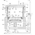
图1是简化的剖面图,其示出具有本发明实施例的处理套组的半导体处理系统;1 is a simplified cross-sectional view illustrating a semiconductor processing system having a processing kit according to an embodiment of the present invention;
图2是连接图1的靶材和配接器的处理套组的一个实施例的部分剖面图;Figure 2 is a partial cross-sectional view of one embodiment of a processing kit coupled to the target and adapter of Figure 1;
图3是连接图1的靶材和配接器的处理套组的一个实施例的部分剖面图;Figure 3 is a partial cross-sectional view of one embodiment of a processing kit coupled to the target and adapter of Figure 1;
图4是连接图1的处理系统的处理套组的一个实施例的部分剖面图;Figure 4 is a partial cross-sectional view of one embodiment of a treatment kit coupled to the treatment system of Figure 1;
图5A是俯视图,其示出根据本发明实施例的一件屏蔽;Figure 5A is a top view showing a piece of shielding in accordance with an embodiment of the present invention;
图5B是侧视图,其示出图5A的一件屏蔽的一个实施例;Figure 5B is a side view showing one embodiment of the one piece shield of Figure 5A;
图5C是剖面图,其示出图5A的一件屏蔽的一个实施例;Figure 5C is a cross-sectional view showing one embodiment of the one-piece shield of Figure 5A;
图5D是仰视图,其示出图5A的一件屏蔽的一个实施例;Figure 5D is a bottom view showing one embodiment of the one piece shield of Figure 5A;
图6A是俯视图,其示出根据本发明实施例的隔离环;Figure 6A is a top view showing a spacer ring according to an embodiment of the present invention;
图6B是侧视图,其示出图6A的隔离环的一个实施例;Figure 6B is a side view showing one embodiment of the spacer ring of Figure 6A;
图6C是剖面图,其示出图6A的隔离环的一个实施例;Figure 6C is a cross-sectional view illustrating one embodiment of the spacer ring of Figure 6A;
图6D是仰视图,其示出图6A的隔离环的一个实施例。Figure 6D is a bottom view showing one embodiment of the spacer ring of Figure 6A.
为了便于理解,已经在可能的情况下,使用相同的组件符号指示各图式中相同的组件。意即,在一个实施例中所揭示的组件亦可用于其它实施例而无需特别指明。For ease of understanding, the same reference numerals have been used, where possible, to designate the same components in the various drawings. That is to say, components disclosed in one embodiment can also be used in other embodiments without special specification.
具体实施方式Detailed ways
本发明的实施例大体上提供处理套组,以用于物理沉积(PVD)室。在一个实施例中,该处理套组提供减少的射频返回路径,从而减少在处理腔外引起的射频谐波和杂散等离子体,因而促成较大的均匀度、可重复性、和较长的室组件可用寿命。在一个实施例中,该处理套组提供隔离环,其设计为减少在腔壁和靶材间的电短路。Embodiments of the invention generally provide processing kits for use in physical deposition (PVD) chambers. In one embodiment, the processing kit provides a reduced RF return path, thereby reducing RF harmonics and stray plasma induced outside the processing chamber, thereby facilitating greater uniformity, repeatability, and longer useful life of chamber components. In one embodiment, the processing kit provides spacer rings designed to reduce electrical shorting between the chamber walls and the target.
图1示出示例性半导体处理室100,其具有能够处理基板105的处理套组150的一个实施例。该处理套组150包括一件接地屏蔽160、交错盖环170、和隔离环180。如图所示,处理室100包含溅射室,也称为物理气相沉积或PVD室,其能够在基板上沉积钛或铝氧化物。处理室100也可用于其它目的,例如,沉积铝、铜、钽、氮化钽、碳化钽、钨、钨氮化物、镧、镧氧化物和钛。可适于受益于本发明的处理室的一个例子是

处理室100包括室主体101,其具有封闭壁壁102和侧壁104、底壁106和盖组件108,其包覆内部容积110或等离子体区。室主体101通常是由焊接的不锈钢板或单铝块制成。在一个实施例中,侧壁包含铝,及底壁包括不锈钢。侧壁104一般包含狭缝阀(未图示),以供基板105进出处理室100。处理室100的盖组件108与和盖环170交错的接地屏蔽160共同作用,将形成在内部容积110中的等离子体限定到基板上的区域。The
室100的底壁106支撑基座组件120。在处理中,基座组件120支撑沉积环302及基板105。升降机构122经配置以在上部和下部位置间移动基座组件120,藉由该升降机构122,基座组件120连接至室100的底壁106。此外,在较低的位置,经由基座组件120移动举升销以使基板与基座组件120隔开,以便于基板与设置在处理室100的外的晶圆传输机构(例如,单刀机器手臂(未图示))的交换。通常将折箱124放置基座组件120和室底壁106之间,以将室主体101的内部容积110与基座组件120的内部和室的外部隔离。The
基座组件120一般包括基板支撑126,密封耦合至平台外壳128。该平台外壳128通常由金属材料(如不锈钢或铝)所制造。冷却板(未图示)一般放置于平台外壳128内,以热调节基板支撑126。在美国专利第5,507,499号(1996年4月16日授予专利予Davenport等)中描述了可适于从本文的实施例受益的基座组件120,通过全文引用包含在本文中。The
基板支撑126可包括铝或陶瓷。基板支撑126具有基板接收表面127,其在处理中接收并支撑基板105,表面127具有平面,其实质上平行于靶材132的溅射表面133。支撑126也有外缘129,其终止于基板105的悬垂边缘。基板支撑126可以是静电夹头、陶瓷主体、加热器、或其结合。在一个实施例中,基板支撑126是静电夹头,其包括介电主体,其具有导电层嵌入其中。介电主体通常是由高导热介电材料所制成,例如,热解氮化硼、氮化铝、氮化硅、氧化铝或同等材料。
盖组件108一般包括盖130、靶材132、和磁控管134。当在如图1所示的封闭位置时,盖130被侧壁104支撑。陶瓷环密封136被置于隔离环180、盖130及侧壁104之间,以防止其中的真空泄漏。
靶材132连接盖130并曝露至处理室100的内部容积110。在PVD处理中,靶材132提供用来沉积在基材上的材料。隔离环180被配置在靶材132、盖130、和室主体101之间,以将靶材132与盖130和室主体101电气隔离。The
通过电源140,靶材132相对于接地(例如,室主体101和配接器220)偏压。气体(例如,氩)从气源142通过导管144提供给内部容积110。气源142可包括非活性气体(例如,氩气或氙气),其能够大力撞击并从靶材132溅射材料。气源142亦可包括反应气体,例如,含氧气体、含氮气体、含甲烷气体的一种或多种,其能够与溅射材料反应,以在基板上形成层材料。使用过的处理气体和副产品,从室100通过排气口146排出,排气口146接收使用过的处理气体并将使用过的处理气体导引至具有节流阀的排气导管148,以控制室100中气体压力。排气导管148连接到一个或多个排气泵149。一般而言,室100中溅射气体的压力被设置为低于大气水平,例如,真空环境,例如,0.6mTorr至400mTorr的气体压力。等离子体由气体形成于基板105和靶材132之间。等离子体中离子朝向靶材132被加速并使材料从靶材132移出。被移出的靶材材料被沉积在基板上。Via
磁控管134连接处理室100外部上的盖130。在美国专利第5,953,827号(1999年9月21日授予专利予Or等)中描述了可用的磁控管,通过全文引用结合于此。The
室100被控制器190所控制,该控制器190包含具有指令集的程序代码,以操作室100的组件,以处理室100中的基板。例如,控制器190可包含程序代码,其包括:基板定位指令集,以操作基座组件120;气体流量控制指令集,以操作气体流量控制阀,以设定流至室100的溅射气体的流量;气体压力控制指令集,其操作节流阀,以保持室100中的压力;温度控制指令集,以控制基座组件120或侧壁104中的温度控制系统(未图示),以分别设定基板或侧壁104的温度;和处理监测指令集,其监测室100中处理。The
室100还包含处理套组150,其包括各种可以很容易地从室100移除的组件,例如,用来清洁组件表面的溅射沉积、更换或修理被侵蚀的组件,或调整室100以适应其它处理。在一个实施例中,处理套组150包括隔离器180、接地屏蔽160和环组件168,以配置基板支撑126的周边129,其终止于基板105的悬垂边缘。
屏蔽160围绕溅射靶材132的溅射表面133,其面向基板支撑126和基板支撑126的周边129。屏蔽160涵盖和遮蔽室100的侧壁104,以减少来自溅射靶材132的溅射表面133的溅射沉积被沉积至屏蔽160的后的组件和表面上。例如,屏蔽160可以保护室100的支撑126、基板105的悬垂边缘、侧壁104和底壁106的表面。
如图1、5A、5B、5C、和5D所示,屏蔽160是统一结构并包括圆柱形外环带210,其直径的尺寸为包围溅射靶材132的溅射表面133和基板支撑126。在一个实施例中,圆柱形外环带210具有以箭头“A”表示的内径。在一个实施例中,圆柱形外环带210的内径“A”介于约16英寸(40.6cm)和约18英寸(45.7cm)之间。在另一实施例中,圆柱形外环带210的内径“A”介于约16.8英寸(42.7cm)和约17英寸(43.2cm)之间。在一个实施例中,圆柱形外环带210具有以箭头“B”表示的外径。在一个实施例中,圆柱形外环带210的外径“B”介于约17英寸(43.2cm)和约19英寸(48.3cm)之间。在另一实施例中,圆柱形外环带210的外径“B”介于约17.1英寸(43.4cm)和约17.3英寸(43.9cm)之间。As shown in FIGS. 1 , 5A, 5B, 5C, and 5D,
圆柱形外环带210具有:顶端212,其包围溅射靶材132的溅射表面133;和底端213,其围绕基板支撑126。倾斜阶214从圆柱形外环带210的顶端212径向向外延伸。在一个实施例中,倾斜阶214相对于竖直方向形成角度“α”。在一个实施例中,角度“α”相对于竖直介于约15度至约25度之间。在另一实施例中,倾斜角度“α”是大约20度。Cylindrical
在一个实施例中,屏蔽160具有高度“C”,其介于约10英寸和12英寸之间。在另一实施例中,屏蔽160具有高度“C”,其介于约11英寸(27.9cm)和11.5英寸(29.2cm)之间。在另一实施例中,屏蔽160具有高度“C”,其介于约7英寸(17.8cm)和8英寸(20.3cm)之间。在另一实施例中,屏蔽具有高度“C”,其介于约7.2英寸(18.3cm)和7.4英寸(18.8cm)之间。In one embodiment,
固定凸缘216从圆柱形外环带210的倾斜阶214径向向外延伸。参照图2和图5C,该固定凸缘包含较低接触面218,以置于包围室100的侧壁104的环形配接器220上,还包含较高接触面219。在一个实施例中,固定凸缘216的较低接触面218包含多个柱坑(未图示),其形状和大小适于接收螺钉,以将屏蔽160附接至配接器220。如图2所示,较高接触面219的内周边217形成阶221。该阶221提供迷宫间隙,其防止导电材料在隔离环180和屏蔽160之间产生表面桥,从而保持电性不导通。A securing
在一个实施例中,该配接器220支撑屏蔽160并可作为基板处理室100的侧壁104的热交换器。配接器220和屏蔽160形成组件,其改善来自屏蔽160的热传导,且减少沉积在屏蔽上的材料的热膨胀应力。通过曝露至在基板处理室100中形成的等离子体,使屏蔽160的部分高度加热,使得屏蔽热膨胀,并使形成在屏蔽上的溅射沉积从屏蔽脱离,落至并污染基板105。配接器220有放置面222,其接触屏蔽160的较低接触面218,以允许屏蔽160和配接器220间良好的电和热传导率。在一个实施例中,配接器220还包括导管,其使传热流体从中流过,以控制配接器220的温度。In one embodiment, the
参照图1、4、5A、5B、5C、和5D,圆柱形外环带210还包括低端213,其围绕基板支撑126。基盘224从圆柱形外环带210的底端213径向向内延伸。圆柱形内环带226连接至基盘224,并至少部分围绕基板支撑126的周边129。在实施例中,圆柱形内环带具有以箭头“D”表示的直径。在一个实施例中,圆柱形内环带226具有直径“D”,其介于约14英寸(35.6cm)和约16英寸(40.6cm)之间。在另一实施例中,圆柱形内环带226具有直径“D”,其介于约14.5英寸(36.8cm)和约15英寸(38.1cm)之间。圆柱形内环带226从基板224向上延伸并垂直于基板224。圆柱形内环带226、基盘224、和圆柱形外环带210形成U形信道。圆柱形内环带226包括高度,其小于圆柱外环带210的高度。在一个实施例中,内环带226的高度是圆柱形外环带210的大约五分之一。在一个实施例中,圆柱形内环带226具有以箭头“E”表示的高度。在一个实施例中,圆柱形内环带226的高度“E”介于约0.8英寸(2cm)和约1.3英寸(3.3cm)之间。在另一实施例中,圆柱形内环带226的高度“E”介于约1.1英寸(2.8cm)和约1.3英寸(3.3cm)之间。在另一实施例中,圆柱形内环带226的高度介于约0.8英寸(2cm)和约0.9英寸(2.3cm)之间。Referring to FIGS. 1 , 4 , 5A, 5B, 5C, and 5D, the cylindrical
圆柱形外环带210、倾斜阶214、固定凸缘216、基盘224和圆柱内环带226包含统一结构。例如,在一个实施例中,整个屏蔽160可以由铝制成,或在另一实施例中,由300系列的不锈钢制成。统一屏蔽160优于使用包括多个组件(往往二或三个单独组件)制成整个屏蔽的传统屏蔽。现有的多部分屏蔽提供延伸的射频返回路径,其造成引起处理腔外杂散等离子体的射频谐波;相比的下,本发明的统一屏蔽减少射频返回路径,因此在内部处理区域提供改进的等离子体包容。具有多个组件的屏蔽160较难且较费力移除屏蔽进行清洁。一件式屏蔽160具有曝露至溅射沉积的连续表面,而没有难以清理的接面或角落。一件式屏蔽160也能更有效地遮蔽室壁壁104,防止处理中的溅射沉积。在一个实施例中,消除了传导特征,例如,导洞。消除传导特征减少了内部容积110外的杂散等离子体的形成。Cylindrical
在一个实施例中,屏蔽160的曝露表面以CLEANCOATTM来处理,该机器可获取自应用材料(美国加州圣大克劳拉市)。CLEANCOATTM是种双股铝电弧喷涂,其应用于基板处理室组件,例如,屏蔽160,以减少粉粒脱落沉积在屏蔽160上,从而防止污染室100中的基板105。在一个实施例中,喷涂在该屏蔽160上的该双股铝电弧喷涂涂层具有表面粗糙度,其介于约600至约2300微英寸。In one embodiment, the exposed surface of
屏蔽160具有朝向室100中的内部容积110的曝露表面。在一个实施例中,曝露表面经“珠击”以具有表面粗糙度175±75微英寸。形成纹理的珠击表面可减少粉粒脱落并防止室100内的污染。表面粗糙度平均是沿曝露表面的粗糙度特征的峰值和谷值的平均线的位移的绝对值。粗糙度平均、偏斜、或其它特性可由轮廓仪决定,其使针在该曝露表面上通过,并产生表面上粗糙的高度的波动轨迹,或通过扫描电子显微镜,利用从表面反射的电子束来产生该表面的影像。
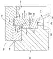
参照图3,在一个实施例中,隔离环180是L形。隔离环180包括环形带,其延伸并包围靶材132的溅射表面133。隔离环180电性隔离和分隔靶材132与屏蔽160,且通常由介电或绝缘材料所制成,例如,氧化铝。隔离环180包括较低水平部分232和从该较低水平部分232向上延伸的垂直部分234。较低水平部分232包含内周235、外周236、底部接触面237、和顶面238,其中该较低水平部分232的该底部接触面237接触固定凸缘216的较高接触面219。在一个实施例中,该屏蔽160的较高接触面219形成阶233。该阶233提供迷宫间隙,其防止导电材料在隔离环180和屏蔽160之间产生表面桥,从而保持电性不导通。隔离环180的较高垂直部分234包括内周239、外周240和顶面241。较高垂直部分234的该内周239和较低水平部分232的内周235形成统一表面。较低水平部分232的顶面238和较高垂直部分234的外周240垂直相交于过渡点242,以形成阶243。在一个实施例中,阶243与环密封136和靶材132形成迷宫间隙。Referring to FIG. 3 , in one embodiment, the
在一个实施例中,隔离环180具有内径,其由内周235和内周239所界定,其介于约17.5英寸(44.5cm)和约18英寸(45.7cm)之间。在另一实施例中,隔离环180具有内径,其介于约17.5英寸(44.5cm)和17.7英寸(45cm)之间。在一个实施例中,隔离环180具有外径,其由较低水平部分232的外周236所界定,其介于约18英寸(45.7cm)和约19英寸(48.3cm)之间。在另一实施例中,隔离环180具有外径,其介于约18.7英寸(47.5cm)和19英寸(48.3cm)之间。在另一实施例中,隔离环180具有第二外径,其由较低水平部分234的外周240所界定,其介于约18英寸(45.7cm)和约18.5英寸(47cm)之间。在另一实施例中,第二外径介于约18.2英寸(46.2cm)和约18.4英寸(46.7cm)之间。在一个实施例中,隔离环180具有高度,其介于约1英寸(2.5cm)和1.5英寸(3.8cm)之间。在另一实施例中,隔离环180具有高度,其介于约1.4英寸(3.6cm)和1.45英寸(3.7cm)之间。In one embodiment,
在一个实施例中,曝露表面(包括顶面241和垂直部分234的内周、内周235和隔离器180的较低水平部分232的底部接触面237)经过例如喷砂的纹理化处理,使表面粗糙度达180±20Ra,以提供较低沉积和较低应力薄膜的合适的纹理。In one embodiment, the exposed surfaces (including the
其参考图2、6A、6B、6C和6D的另一实施例,隔离环280是T形。隔离环280包括环形带250,其延伸围绕靶材132的溅射表面133。该隔离环280的该环形带250包括:顶壁252,其具有第一宽度;底壁254,其具有第二宽度;及支撑缘256,其具有第三宽度且从该环形带250的该顶壁252径向向外延伸。在一个实施例中,第一宽度少于第三宽度,但大于第二宽度。在一个实施例中,隔离环280具有外径“F”,其介于约18.5英寸(47cm)和约19英寸(48.3cm)之间。在一个实施例中,隔离环280具有外径“F”,其介于约18.8英寸(47.8cm)和约18.9英寸(48cm)之间。Referring to another embodiment of Figures 2, 6A, 6B, 6C and 6D, the
顶壁252包括内周258、邻近靶材132的顶面260、和邻近环密封136的外周262。支撑缘256包括底部接触面264和上表面266。支撑缘256的底部接触面264在铝环267的上。在某些实施例中没有铝环267,且配接器220被配置为支撑该支撑缘256。底壁254包括内周268、外周270和底部表面272。底壁254的内周268和顶壁252的内周258形成统一表面。在一个实施例中,隔离器280具有内径“G”,其由底壁254的内周268和顶壁252的内周258所界定,介于约17英寸(43.2cm)和约18英寸(45.7cm)之间。在另一实施例中,隔离器280的内径“G”介于约17.5英寸(44.5cm)和约17.8英寸(45.2cm)之间。Top wall 252 includes an
垂直沟槽276形成于过渡点278,其介于底壁254的的外周270和支撑缘256的底部接触面264。屏蔽160的阶221结合垂直沟槽276提供迷宫间隙,其防止导电材料在隔离环280和屏蔽160之间产生表面桥,从而保持电气不连续性而对室壁壁104提供遮蔽。在一个实施例中,隔离环280在个靶材132和处理套组150的接地组件之间提供间隙,同时对室壁壁提供遮蔽。在一个实施例中,靶材132和屏蔽160之间的间隙介于约1英寸(2.5cm)和约2英寸(5.1cm)之间,例如,大约1英寸(2.5cm)。在另一实施例中,靶材132和屏蔽160之间的间隙介于约1.1英寸(2.8cm)和约1.2英寸(3cm)之间。在又一实施例中,靶材132和屏蔽160之间的间隙大于约1英寸(2.5cm)。隔离环280的阶梯设计使得屏蔽160能相对于配接器220对中,其中配接器220也是靶材132的配合屏蔽和对齐特征的固定点。阶梯设计也消除从靶材132到屏蔽160的站台直线要求(line-of-site),并消除在此区域的杂散等离子体的顾虑。A vertical groove 276 is formed at a transition point 278 between the outer perimeter 270 of the bottom wall 254 and the bottom contact surface 264 of the
在一个实施例中,隔离环280具有喷砂表面纹理,用以加强薄膜粘性,其具有表面粗糙度180±20Ra,以对较低沉积和较低应力薄膜提供合适的纹理。在一个实施例中,隔离环280具有表面纹理,其通过激光脉冲提供,用以加强薄膜粘性,使具有大于500Ra的表面粗糙度,用于更高沉积厚度和较高薄膜应力。在一个实施例中,当处理室100被用来沉积金属、金属氮化物、金属氧化物、金属碳化物时,经纹理化的表面延长隔离环280的寿命。隔离环280也可自室100移除,其能够回收这部分,而不会影响材料的孔隙度,那可能妨害真空密封应用中的重复使用。支撑缘256使得隔离环280可以相对于配接器220对中,同时消除从靶材132到接地屏蔽160的站台直线要求(line-of-site),因此消除杂散等离子体的顾虑。在一个实施例中,环267包括系列调整销(未图示),其对齐屏蔽160中的系列插槽(未图示)定位。In one embodiment,
参照图4,环组件168包含沉积环302和盖环170。沉积环302包含环带304,其包围支撑126。盖环170至少部分涵盖沉积环302。沉积环302和盖环170相互合作,以减少形成于支撑126的外围边缘129和基板105的悬垂边缘的溅射沉积。Referring to FIG. 4 , the
盖环170包围且至少部分涵盖要接收的沉积环302,及因此在大区块的溅射沉积中遮蔽沉积环302。盖环170由能抵抗溅射等离子体侵蚀的材料制成,例如,金属材料,例如,不锈钢,钛或铝或陶瓷材料,如氧化铝。在一个实施例中,盖环170是由具有纯度至少约百分的九十九点九的钛构成。在一个实施例中,盖环170的表面以双股铝电弧喷涂层处理,例如,CLEANCOATTM,以减少从盖环170表面脱落的粉粒。The
盖环170包括环形楔310,其包括倾斜顶面312,该倾斜顶面312径向向内倾斜,并包围基板支撑126。环形楔310的倾斜顶面312具有内周314和外周316。内周314包括突出边缘318,其覆盖径向向内的凹处,其包含沉积环302的开放的内信道。突出边缘318减少沉积在沉积环302的开放内信道的溅射沉积。在一个实施例中,突出边缘318突出对应于与沉积环302形成的弧形缺口402的至少一半左右宽度的距离。突出边缘318的大小、形状和位置皆配合和符合弧形缺口402,以在盖环170和沉积环302之间形成回旋且限制的流体路径,以抑制处理流体沉积至基板支撑126和平台外壳128上。间隙402的受限的流体路径限制沉积环302和盖环170的相接表面的低能溅射沉积的堆积,否则就会导致它们彼此相粘或粘至基板105的周围悬垂边缘。
倾斜顶面312可倾斜成介于约10度和约20度的角度,例如,相对于水平约16度。盖环170的倾斜顶面312的角度被设计为尽量减少最接近基板105悬垂边缘的溅射沉积的堆积,否则就会对整个基板105所获得的粒子表面产生负面影响。The sloped
盖环170包括脚架320,其从环形楔310的倾斜顶面312向下延伸,以置于沉积环302的支架306上。脚架320从楔310向下延伸至实质上压迫沉积环302,而不会裂开或压裂环302。在一个实施例中,双阶表面形成在脚架320和突出边缘318的较低表面之间。
盖环170还包括内圆柱形环带324a和外圆柱形环带324b,其从环形楔310向下延伸,其间具有间隙。在一个实施例中,内圆柱形环带324a和外圆柱形环带324b实质上垂直。内和外圆柱形环带324a和324b位于环形楔310的脚架320的径向向外。内圆柱形环带324a具有高度,其小于外圆柱形环带324b。一般来说,外圆柱形环带324b的高度是内圆柱形环带324a高度的至少约1.2倍。例如,对于具有约154毫米的内半径的盖环170,外圆柱形环带324b的高度介于约15至约35,或例如,25毫米;并且内圆柱形环带324a的高度介于约12至24毫米,例如,约19毫米。盖环可包括适于化学处理的任何材料,例如,钛或不锈钢。
在一个实施例中,内圆柱形环带324a的表面相对于竖直方向倾斜约12度至约18度。在另一实施例中,内圆柱形环带324a的表面倾斜约15度至约17度。In one embodiment, the surface of the inner
在一个实施例中,盖环170具有外径,其由外圆柱形环带324b所界定,介于约15.5英寸(39.4cm)至约16英寸(40.6cm)之间。在另实施例中,盖环170具有外径,其介于约15.6英寸(39.6cm)至约15.8英寸(40.1cm)之间。在一个实施例中,盖环170具有高度,其介于约1英寸(2.5cm)至1.5英寸(3.8cm)之间。在另一实施例中,盖环170界于约1.2英寸(3cm)至约1.3英寸(3.3cm)之间。In one embodiment,
介于屏蔽160和盖环170之间的空间或间隙404形成回旋S形信道或迷宫,以供等离子体移动。信道的形状是有利的,例如,因为它妨碍和阻碍等离子体类进入到该地区,减少不良溅射材料的沉积。The space or
该处理套组150的组件可独立地及结合地运作,以大幅减少粒子的产生和杂散等离子体。现有的多部分屏蔽提供延伸的射频返回路径,其造成引起处理腔外杂散等离子体的射频谐波;相比之下,上述的一体成形屏蔽减少射频返回路径,因此在内部处理区域提供改进的等离子体包容。一体成形屏蔽的平面基盘通过基座提供RF额外缩短的返回路径,以进一步降低谐波和杂散等离子体以及提供现有接地硬件的平台。一体成形屏蔽还消除了提供射频返回中所有不连续性以及导致处理腔外杂散等离子体的电导特征。修改一体成形屏蔽,以允许隔离环被插入至处理室。隔离环阻挡在地面路径的射频源和处理套组间的视线。修改屏蔽上的固定凸缘,以提供阶和大半径,提供的迷宫防止导电材料在隔离环和屏蔽间产生表面桥,从而保持电气不连续性。通过减少材料的厚度,以便通过流形成来制造,一体成形屏蔽也被设计为降低制造成本。The components of the
虽然上文是针对本发明的实施例,亦可能衍生其它或更进步的实施例,而不偏离本发明基本范畴,本发明的范畴由以下权利要求所界定。Although the above is directed to embodiments of the present invention, other or more advanced embodiments are possible without departing from the basic scope of the present invention, which is defined by the following claims.
Claims (20)
Translated fromChineseApplications Claiming Priority (3)
| Application Number | Priority Date | Filing Date | Title |
|---|---|---|---|
| US5011208P | 2008-05-02 | 2008-05-02 | |
| US61/050,112 | 2008-05-02 | ||
| PCT/US2009/042387WO2009135050A2 (en) | 2008-05-02 | 2009-04-30 | Process kit for rf physical vapor deposition |
Publications (2)
| Publication Number | Publication Date |
|---|---|
| CN102017077A CN102017077A (en) | 2011-04-13 |
| CN102017077Btrue CN102017077B (en) | 2012-09-19 |
Family
ID=41255822
Family Applications (1)
| Application Number | Title | Priority Date | Filing Date |
|---|---|---|---|
| CN2009801158170AActiveCN102017077B (en) | 2008-05-02 | 2009-04-30 | Processing Kits for RF Physical Vapor Deposition |
Country Status (6)
| Country | Link |
|---|---|
| US (2) | US9123511B2 (en) |
| JP (1) | JP5762281B2 (en) |
| KR (1) | KR101511027B1 (en) |
| CN (1) | CN102017077B (en) |
| TW (1) | TWI494454B (en) |
| WO (1) | WO2009135050A2 (en) |
Families Citing this family (29)
| Publication number | Priority date | Publication date | Assignee | Title |
|---|---|---|---|---|
| US8900471B2 (en)* | 2009-02-27 | 2014-12-02 | Applied Materials, Inc. | In situ plasma clean for removal of residue from pedestal surface without breaking vacuum |
| WO2011019566A2 (en)* | 2009-08-11 | 2011-02-17 | Applied Materials, Inc. | Process kit for rf physical vapor deposition |
| CN203103267U (en) | 2010-01-29 | 2013-07-31 | 应用材料公司 | Shields and Handling Kits |
| CN108359957A (en)* | 2010-10-29 | 2018-08-03 | 应用材料公司 | Deposition ring and electrostatic chuck for physical vapor deposition chamber |
| US9905443B2 (en)* | 2011-03-11 | 2018-02-27 | Applied Materials, Inc. | Reflective deposition rings and substrate processing chambers incorporating same |
| JP5772499B2 (en)* | 2011-10-24 | 2015-09-02 | 旭硝子株式会社 | Method for producing a reflective mask blank for EUV lithography (EUVL) and method for producing a substrate with a reflective layer for EUVL |
| CN103882390B (en)* | 2012-12-20 | 2016-04-27 | 北京北方微电子基地设备工艺研究中心有限责任公司 | Reaction chamber and magnetron sputtering equipment |
| WO2014159222A1 (en)* | 2013-03-14 | 2014-10-02 | Applied Materials, Inc. | Methods and apparatus for processing a substrate using a selectively grounded and movable process kit ring |
| US8865012B2 (en) | 2013-03-14 | 2014-10-21 | Applied Materials, Inc. | Methods for processing a substrate using a selectively grounded and movable process kit ring |
| US10096455B2 (en) | 2013-09-17 | 2018-10-09 | Applied Materials, Inc. | Extended dark space shield |
| CN104862660B (en)* | 2014-02-24 | 2017-10-13 | 北京北方华创微电子装备有限公司 | Bogey and plasma processing device |
| US9448261B2 (en)* | 2014-04-11 | 2016-09-20 | General Electric Company | Systems and methods for reducing attenuation in current transducers |
| KR102438139B1 (en) | 2014-12-22 | 2022-08-29 | 어플라이드 머티어리얼스, 인코포레이티드 | Process kit for a high throughput processing chamber |
| JP2018513567A (en) | 2015-04-24 | 2018-05-24 | アプライド マテリアルズ インコーポレイテッドApplied Materials,Incorporated | Process kit including flow isolator ring |
| KR102709229B1 (en)* | 2015-12-07 | 2024-09-23 | 어플라이드 머티어리얼스, 인코포레이티드 | Merge Cover Ring |
| US10577689B2 (en) | 2016-09-23 | 2020-03-03 | Applied Materials, Inc. | Sputtering showerhead |
| US10886113B2 (en) | 2016-11-25 | 2021-01-05 | Applied Materials, Inc. | Process kit and method for processing a substrate |
| WO2019147493A1 (en)* | 2018-01-29 | 2019-08-01 | Applied Materials, Inc. | Process kit geometry for particle reduction in pvd processes |
| CN110838429B (en)* | 2018-08-15 | 2022-07-22 | 北京北方华创微电子装备有限公司 | Cavity lining, plasma reaction chamber and plasma equipment |
| US11361982B2 (en)* | 2019-12-10 | 2022-06-14 | Applied Materials, Inc. | Methods and apparatus for in-situ cleaning of electrostatic chucks |
| CN113035679B (en)* | 2019-12-24 | 2023-09-29 | 中微半导体设备(上海)股份有限公司 | Plasma processing device |
| US11443921B2 (en)* | 2020-06-11 | 2022-09-13 | Applied Materials, Inc. | Radio frequency ground system and method |
| CN113808900B (en)* | 2020-06-17 | 2023-09-29 | 中微半导体设备(上海)股份有限公司 | Plasma processing device and confinement ring assembly and method thereof |
| US11670492B2 (en)* | 2020-10-15 | 2023-06-06 | Applied Materials, Inc. | Chamber configurations and processes for particle control |
| CN115074679B (en)* | 2021-03-11 | 2025-02-11 | 台湾积体电路制造股份有限公司 | Method for forming semiconductor structure and physical vapor deposition device and method |
| CN114446495B (en)* | 2022-01-18 | 2024-08-23 | 大连理工大学 | Inverted sample stage for collecting falling objects for plasma zone |
| CN117012605A (en)* | 2022-04-29 | 2023-11-07 | 中微半导体设备(上海)股份有限公司 | Plasma processing apparatus, spacer, and method of manufacturing the same |
| JP2023183725A (en)* | 2022-06-16 | 2023-12-28 | 東京エレクトロン株式会社 | Film forming equipment |
| US12371790B2 (en)* | 2022-08-17 | 2025-07-29 | Sky Tech Inc. | Wafer carrier with adjustable alignment devices and deposition equipment using the same |
Citations (1)
| Publication number | Priority date | Publication date | Assignee | Title |
|---|---|---|---|---|
| TW512180B (en)* | 2000-09-21 | 2002-12-01 | Promos Technologies Inc | Method for maintaining the cleanness of a vacuum chamber of physical vapor deposition system |
Family Cites Families (42)
| Publication number | Priority date | Publication date | Assignee | Title |
|---|---|---|---|---|
| US5202008A (en)* | 1990-03-02 | 1993-04-13 | Applied Materials, Inc. | Method for preparing a shield to reduce particles in a physical vapor deposition chamber |
| JPH06204323A (en)* | 1992-10-27 | 1994-07-22 | Applied Materials Inc | Clamp ring for domed heated pedestal in wafer process chamber |
| JPH0734236A (en)* | 1993-07-19 | 1995-02-03 | Canon Inc | DC sputtering apparatus and sputtering method |
| US5632873A (en)* | 1995-05-22 | 1997-05-27 | Stevens; Joseph J. | Two piece anti-stick clamp ring |
| US5690795A (en) | 1995-06-05 | 1997-11-25 | Applied Materials, Inc. | Screwless shield assembly for vacuum processing chambers |
| US5697427A (en)* | 1995-12-22 | 1997-12-16 | Applied Materials, Inc. | Apparatus and method for cooling a substrate |
| US5736021A (en) | 1996-07-10 | 1998-04-07 | Applied Materials, Inc. | Electrically floating shield in a plasma reactor |
| US5914018A (en)* | 1996-08-23 | 1999-06-22 | Applied Materials, Inc. | Sputter target for eliminating redeposition on the target sidewall |
| EP0841683A3 (en)* | 1996-10-08 | 1999-12-01 | Applied Materials, Inc. | Active shield for generating a plasma for sputtering |
| EP0954620A4 (en)* | 1997-01-16 | 2002-01-02 | Bottomfield Layne F | Vapor deposition components and corresponding methods |
| US5942042A (en) | 1997-05-23 | 1999-08-24 | Applied Materials, Inc. | Apparatus for improved power coupling through a workpiece in a semiconductor wafer processing system |
| US6051122A (en)* | 1997-08-21 | 2000-04-18 | Applied Materials, Inc. | Deposition shield assembly for a semiconductor wafer processing system |
| KR20010089376A (en) | 1998-10-29 | 2001-10-06 | 조셉 제이. 스위니 | Apparatus for coupling power through a workpiece in a semiconductor wafer processing system |
| KR20000030996A (en) | 1998-11-02 | 2000-06-05 | 윤종용 | Dry type etching plant of semiconductor |
| US6398929B1 (en)* | 1999-10-08 | 2002-06-04 | Applied Materials, Inc. | Plasma reactor and shields generating self-ionized plasma for sputtering |
| JP2001140054A (en) | 1999-11-15 | 2001-05-22 | Nec Kagoshima Ltd | Cleaning method for vacuum film depositing system, and vacuum film depositing system |
| US6589352B1 (en) | 1999-12-10 | 2003-07-08 | Applied Materials, Inc. | Self aligning non contact shadow ring process kit |
| US6394023B1 (en) | 2000-03-27 | 2002-05-28 | Applied Materials, Inc. | Process kit parts and method for using same |
| US6296747B1 (en) | 2000-06-22 | 2001-10-02 | Applied Materials, Inc. | Baffled perforated shield in a plasma sputtering reactor |
| US6699375B1 (en) | 2000-06-29 | 2004-03-02 | Applied Materials, Inc. | Method of extending process kit consumable recycling life |
| US20020090464A1 (en)* | 2000-11-28 | 2002-07-11 | Mingwei Jiang | Sputter chamber shield |
| US7041201B2 (en)* | 2001-11-14 | 2006-05-09 | Applied Materials, Inc. | Sidewall magnet improving uniformity of inductively coupled plasma and shields used therewith |
| US6899798B2 (en) | 2001-12-21 | 2005-05-31 | Applied Materials, Inc. | Reusable ceramic-comprising component which includes a scrificial surface layer |
| US6743340B2 (en) | 2002-02-05 | 2004-06-01 | Applied Materials, Inc. | Sputtering of aligned magnetic materials and magnetic dipole ring used therefor |
| US6730174B2 (en)* | 2002-03-06 | 2004-05-04 | Applied Materials, Inc. | Unitary removable shield assembly |
| US7041200B2 (en) | 2002-04-19 | 2006-05-09 | Applied Materials, Inc. | Reducing particle generation during sputter deposition |
| US6797131B2 (en) | 2002-11-12 | 2004-09-28 | Applied Materials, Inc. | Design of hardware features to facilitate arc-spray coating applications and functions |
| US20050016684A1 (en) | 2003-07-25 | 2005-01-27 | Applied Materials, Inc. | Process kit for erosion resistance enhancement |
| JP2005264177A (en)* | 2004-03-16 | 2005-09-29 | Renesas Technology Corp | Sputtering apparatus, and upper shield position adjusting method of the same |
| US7579067B2 (en) | 2004-11-24 | 2009-08-25 | Applied Materials, Inc. | Process chamber component with layered coating and method |
| US9127362B2 (en) | 2005-10-31 | 2015-09-08 | Applied Materials, Inc. | Process kit and target for substrate processing chamber |
| US20070116872A1 (en)* | 2005-11-18 | 2007-05-24 | Tokyo Electron Limited | Apparatus for thermal and plasma enhanced vapor deposition and method of operating |
| US8647484B2 (en) | 2005-11-25 | 2014-02-11 | Applied Materials, Inc. | Target for sputtering chamber |
| US7520969B2 (en) | 2006-03-07 | 2009-04-21 | Applied Materials, Inc. | Notched deposition ring |
| US20070283884A1 (en)* | 2006-05-30 | 2007-12-13 | Applied Materials, Inc. | Ring assembly for substrate processing chamber |
| US8221602B2 (en) | 2006-12-19 | 2012-07-17 | Applied Materials, Inc. | Non-contact process kit |
| US7981262B2 (en) | 2007-01-29 | 2011-07-19 | Applied Materials, Inc. | Process kit for substrate processing chamber |
| US8062487B2 (en)* | 2007-06-25 | 2011-11-22 | United Microelectronics Corp. | Wafer supporting device of a sputtering apparatus |
| KR102025330B1 (en)* | 2008-04-16 | 2019-09-25 | 어플라이드 머티어리얼스, 인코포레이티드 | Wafer processing deposition shielding components |
| WO2011019566A2 (en)* | 2009-08-11 | 2011-02-17 | Applied Materials, Inc. | Process kit for rf physical vapor deposition |
| CN203103267U (en)* | 2010-01-29 | 2013-07-31 | 应用材料公司 | Shields and Handling Kits |
| CN108359957A (en)* | 2010-10-29 | 2018-08-03 | 应用材料公司 | Deposition ring and electrostatic chuck for physical vapor deposition chamber |
- 2009
- 2009-04-30CNCN2009801158170Apatent/CN102017077B/enactiveActive
- 2009-04-30KRKR1020107027130Apatent/KR101511027B1/enactiveActive
- 2009-04-30JPJP2011507660Apatent/JP5762281B2/enactiveActive
- 2009-04-30USUS12/433,315patent/US9123511B2/enactiveActive
- 2009-04-30WOPCT/US2009/042387patent/WO2009135050A2/enactiveApplication Filing
- 2009-05-01TWTW098114656Apatent/TWI494454B/enactive
- 2012
- 2012-04-26USUS13/457,438patent/US8668815B2/enactiveActive
Patent Citations (1)
| Publication number | Priority date | Publication date | Assignee | Title |
|---|---|---|---|---|
| TW512180B (en)* | 2000-09-21 | 2002-12-01 | Promos Technologies Inc | Method for maintaining the cleanness of a vacuum chamber of physical vapor deposition system |
Also Published As
| Publication number | Publication date |
|---|---|
| US8668815B2 (en) | 2014-03-11 |
| TW201000664A (en) | 2010-01-01 |
| CN102017077A (en) | 2011-04-13 |
| WO2009135050A2 (en) | 2009-11-05 |
| JP5762281B2 (en) | 2015-08-12 |
| US9123511B2 (en) | 2015-09-01 |
| JP2011520034A (en) | 2011-07-14 |
| KR101511027B1 (en) | 2015-04-10 |
| KR20110021840A (en) | 2011-03-04 |
| WO2009135050A3 (en) | 2010-02-18 |
| US20090272647A1 (en) | 2009-11-05 |
| US20120205241A1 (en) | 2012-08-16 |
| TWI494454B (en) | 2015-08-01 |
Similar Documents
| Publication | Publication Date | Title |
|---|---|---|
| CN102017077B (en) | Processing Kits for RF Physical Vapor Deposition | |
| JP5916384B2 (en) | Wafer processing deposit shielding component | |
| JP5611350B2 (en) | Process kit for RF physical vapor deposition | |
| US9978569B2 (en) | Adjustable process spacing, centering, and improved gas conductance | |
| US9689070B2 (en) | Deposition ring and electrostatic chuck for physical vapor deposition chamber | |
| US9062379B2 (en) | Wafer processing deposition shielding components |
Legal Events
| Date | Code | Title | Description |
|---|---|---|---|
| C06 | Publication | ||
| PB01 | Publication | ||
| C10 | Entry into substantive examination | ||
| SE01 | Entry into force of request for substantive examination | ||
| C14 | Grant of patent or utility model | ||
| GR01 | Patent grant |