CN102013240A - Liquid crystal display device, driving method and electronic device - Google Patents
Liquid crystal display device, driving method and electronic deviceDownload PDFInfo
- Publication number
- CN102013240A CN102013240ACN2010102775092ACN201010277509ACN102013240ACN 102013240 ACN102013240 ACN 102013240ACN 2010102775092 ACN2010102775092 ACN 2010102775092ACN 201010277509 ACN201010277509 ACN 201010277509ACN 102013240 ACN102013240 ACN 102013240A
- Authority
- CN
- China
- Prior art keywords
- liquid crystal
- aforementioned
- period
- voltage
- signal
- Prior art date
- Legal status (The legal status is an assumption and is not a legal conclusion. Google has not performed a legal analysis and makes no representation as to the accuracy of the status listed.)
- Pending
Links
- 239000004973liquid crystal related substanceSubstances0.000titleclaimsabstractdescription137
- 238000000034methodMethods0.000titleclaimsabstractdescription15
- 230000004044responseEffects0.000claimsabstractdescription20
- 230000003287optical effectEffects0.000claimsabstractdescription17
- 238000002834transmittanceMethods0.000claimsdescription26
- 230000008859changeEffects0.000claimsdescription12
- 230000005684electric fieldEffects0.000abstractdescription20
- 230000007423decreaseEffects0.000abstractdescription5
- 239000000758substrateSubstances0.000description16
- 238000006243chemical reactionMethods0.000description15
- 238000010586diagramMethods0.000description11
- 239000003990capacitorSubstances0.000description5
- 230000007547defectEffects0.000description4
- 230000002087whitening effectEffects0.000description4
- 239000003086colorantSubstances0.000description3
- 239000010408filmSubstances0.000description2
- 230000004048modificationEffects0.000description2
- 238000012986modificationMethods0.000description2
- 230000009467reductionEffects0.000description2
- 239000010409thin filmSubstances0.000description2
- 238000005282brighteningMethods0.000description1
- 230000000694effectsEffects0.000description1
- 229910052736halogenInorganic materials0.000description1
- 150000002367halogensChemical class0.000description1
- 239000011159matrix materialSubstances0.000description1
- 230000008569processEffects0.000description1
- 238000005070samplingMethods0.000description1
- 230000001629suppressionEffects0.000description1
- 230000001360synchronised effectEffects0.000description1
Images


Classifications
- G—PHYSICS
- G09—EDUCATION; CRYPTOGRAPHY; DISPLAY; ADVERTISING; SEALS
- G09G—ARRANGEMENTS OR CIRCUITS FOR CONTROL OF INDICATING DEVICES USING STATIC MEANS TO PRESENT VARIABLE INFORMATION
- G09G3/00—Control arrangements or circuits, of interest only in connection with visual indicators other than cathode-ray tubes
- G09G3/20—Control arrangements or circuits, of interest only in connection with visual indicators other than cathode-ray tubes for presentation of an assembly of a number of characters, e.g. a page, by composing the assembly by combination of individual elements arranged in a matrix no fixed position being assigned to or needed to be assigned to the individual characters or partial characters
- G09G3/34—Control arrangements or circuits, of interest only in connection with visual indicators other than cathode-ray tubes for presentation of an assembly of a number of characters, e.g. a page, by composing the assembly by combination of individual elements arranged in a matrix no fixed position being assigned to or needed to be assigned to the individual characters or partial characters by control of light from an independent source
- G09G3/36—Control arrangements or circuits, of interest only in connection with visual indicators other than cathode-ray tubes for presentation of an assembly of a number of characters, e.g. a page, by composing the assembly by combination of individual elements arranged in a matrix no fixed position being assigned to or needed to be assigned to the individual characters or partial characters by control of light from an independent source using liquid crystals
- G09G3/3611—Control of matrices with row and column drivers
- G09G3/3648—Control of matrices with row and column drivers using an active matrix
- H—ELECTRICITY
- H04—ELECTRIC COMMUNICATION TECHNIQUE
- H04N—PICTORIAL COMMUNICATION, e.g. TELEVISION
- H04N9/00—Details of colour television systems
- H04N9/12—Picture reproducers
- H04N9/31—Projection devices for colour picture display, e.g. using electronic spatial light modulators [ESLM]
- H04N9/3102—Projection devices for colour picture display, e.g. using electronic spatial light modulators [ESLM] using two-dimensional electronic spatial light modulators
- H04N9/3105—Projection devices for colour picture display, e.g. using electronic spatial light modulators [ESLM] using two-dimensional electronic spatial light modulators for displaying all colours simultaneously, e.g. by using two or more electronic spatial light modulators
- H—ELECTRICITY
- H04—ELECTRIC COMMUNICATION TECHNIQUE
- H04N—PICTORIAL COMMUNICATION, e.g. TELEVISION
- H04N9/00—Details of colour television systems
- H04N9/12—Picture reproducers
- H04N9/31—Projection devices for colour picture display, e.g. using electronic spatial light modulators [ESLM]
- H04N9/3102—Projection devices for colour picture display, e.g. using electronic spatial light modulators [ESLM] using two-dimensional electronic spatial light modulators
- H04N9/312—Driving therefor
- G—PHYSICS
- G09—EDUCATION; CRYPTOGRAPHY; DISPLAY; ADVERTISING; SEALS
- G09G—ARRANGEMENTS OR CIRCUITS FOR CONTROL OF INDICATING DEVICES USING STATIC MEANS TO PRESENT VARIABLE INFORMATION
- G09G2310/00—Command of the display device
- G09G2310/08—Details of timing specific for flat panels, other than clock recovery
Landscapes
- Engineering & Computer Science (AREA)
- Multimedia (AREA)
- Signal Processing (AREA)
- Chemical & Material Sciences (AREA)
- Crystallography & Structural Chemistry (AREA)
- Physics & Mathematics (AREA)
- Computer Hardware Design (AREA)
- General Physics & Mathematics (AREA)
- Theoretical Computer Science (AREA)
- Control Of Indicators Other Than Cathode Ray Tubes (AREA)
- Liquid Crystal (AREA)
- Liquid Crystal Display Device Control (AREA)
Abstract
Translated fromChineseDescription
Translated fromChinese技术领域technical field
本发明涉及减轻液晶显示装置的显示上的不良状况的技术。The present invention relates to a technique for alleviating display defects of a liquid crystal display device.
背景技术Background technique
液晶面板成为下述结构:以在一个基板上每像素地像素电极排列为矩阵状、在另一个基板上共用电极遍及各像素而成为共用的方式设置,由像素电极与共用电极夹持液晶。如果使与灰度等级相应的电压施加、保持在像素电极与共用电极之间,则液晶的取向状态按每一像素被规定,由此,透射率或反射率被控制。因此,上述结构,能够使作用于液晶分子的电场之中、仅从像素电极朝向共用电极的方向(或其相反方向)、即相对于基板面的垂直方向(纵方向)的分量,对显示控制起作用。A liquid crystal panel has a structure in which pixel electrodes per pixel are arranged in a matrix on one substrate, and a common electrode is provided in common across each pixel on the other substrate, and liquid crystal is sandwiched between the pixel electrodes and the common electrode. By applying and holding a voltage corresponding to the gray scale between the pixel electrode and the common electrode, the alignment state of the liquid crystal is specified for each pixel, thereby controlling the transmittance or reflectance. Therefore, the above-mentioned structure can make the electric field acting on the liquid crystal molecules, only the direction from the pixel electrode toward the common electrode (or its opposite direction), that is, the component in the vertical direction (longitudinal direction) with respect to the substrate surface, contribute to the display control. kick in.
如果如近年来那样为了小型化、高精细化而使像素间距变窄,则会产生在相互相邻的像素电极之间产生的电场、即相对于基板面的平行方向(横方向)的电场,其影响不能忽视。如果对例如像VA(Vertical Alignment,垂直取向)方式和/或TN(Twisted Nematic,扭曲向列)方式等那样应该由纵方向的电场所驱动的液晶施加横电场,则会产生下述问题:液晶变得取向不良(反向倾斜域(リバ一スチルトドメイン))、产生显示上的不良状况。If the pixel pitch is narrowed for miniaturization and high definition as in recent years, an electric field generated between adjacent pixel electrodes, that is, an electric field in a direction parallel to the substrate surface (horizontal direction) is generated, Its impact cannot be ignored. If, for example, a horizontal electric field is applied to a liquid crystal that should be driven by an electric field in the vertical direction, such as VA (Vertical Alignment, vertical alignment) method and/or TN (Twisted Nematic, twisted nematic) method, the following problems will occur: The alignment becomes poor (reverse tilt domain (reverse tilt domain)), and a defect in display occurs.
为了减轻该反向倾斜域的影响,提出了以下技术:与像素电极一致地规定遮光层(开口部)的形状等而改进液晶面板的结构的技术(例如参照专利文献1),在根据图像信号计算出的平均亮度值小于等于阈值的情况下判断为产生反向倾斜域而削除大于等于设定值的图像信号的技术(例如参照专利文献2)等。In order to reduce the influence of this reverse tilt domain, the following technology has been proposed: the technology of improving the structure of the liquid crystal panel by defining the shape of the light shielding layer (opening) in accordance with the pixel electrode (for example, refer to Patent Document 1), and the following technology is proposed in accordance with the image signal When the calculated average luminance value is equal to or less than a threshold value, it is determined that a reverse slope region is generated and the image signal equal to or greater than a set value is eliminated (for example, refer to Patent Document 2).
[专利文献1]特开平6-34965号公报(图1)[Patent Document 1] JP-A-6-34965 (FIG. 1)
[专利文献2]特开2009-69608号公报(图2)[Patent Document 2] JP-A-2009-69608 (FIG. 2)
但是,通过液晶面板的结构而减少反向倾斜域的技术,存在着容易使开口率降低、此外不能够应用于未改进结构而已经制作的液晶面板的缺点。另一方面,削除大于等于设定值的图像信号的技术,也存在着所显示的图像的明亮度被限制为设定值的缺点。However, the technique of reducing the reverse tilt domain by the structure of the liquid crystal panel has the disadvantage that the aperture ratio tends to decrease, and it cannot be applied to liquid crystal panels that have already been manufactured without improving the structure. On the other hand, the technique of cutting out image signals greater than or equal to the set value also has the disadvantage that the brightness of the displayed image is limited to the set value.
发明内容Contents of the invention
本发明是鉴于上述的情形而提出的,其目的之一在于提供消除这些缺点并且减少反向倾斜域的技术。The present invention is made in view of the above circumstances, and one of its objects is to provide a technology that eliminates these disadvantages and reduces the reverse tilt domain.
为了达到上述目的,本发明的液晶显示装置,具有:像素,其对应于多条扫描线与多条数据线的交叉处而设置,各个像素具有利用像素电极与共用电极挟持液晶的液晶元件以及在对前述扫描线施加选择电压时、使前述像素电极与前述数据线之间成为导通状态的开关元件;扫描线驱动电路,其以在时间上设有间隔的图像写入期间选择前述多条扫描线,对所选择的扫描线施加前述选择电压,对于前述多条扫描线之中的一扫描线,在置位期间进行选择,对所选择的扫描线施加前述选择电压,该置位期间比在前述图像写入期间对该扫描线施加前述选择电压的定时提前预定时间且包含于前述间隔中;数据线驱动电路,其在前述图像写入期间,经由前述数据线对前述像素提供与图像信号相应的电压的数据信号,在前述置位期间,经由前述数据线对前述像素提供预定电压的置位信号;前述预定时间,比前述液晶元件的透射率或反射率从0%变化为100%时所需要的响应时间或从100%变化为0%时所需要的响应时间短。根据本发明,可以实现反向倾斜域的减少。此时,由于不会发生开口率的下降,所以也可以应用于未改进结构而已经制作的液晶面板,此外,所显示的图像的明亮度也不会被限制于设定值。In order to achieve the above object, the liquid crystal display device of the present invention has: pixels, which are arranged corresponding to the intersections of a plurality of scanning lines and a plurality of data lines, and each pixel has a liquid crystal element that pinches the liquid crystal by a pixel electrode and a common electrode; a switching element for bringing the pixel electrode and the data line into a conduction state when a selection voltage is applied to the scanning line; line, apply the aforementioned selection voltage to the selected scanning line, select one of the aforementioned plurality of scanning lines during the setting period, apply the aforementioned selection voltage to the selected scanning line, and the setting period is more than that during the setting period. Timing of applying the selection voltage to the scanning line during the image writing period is advanced by a predetermined time and included in the interval; a data line driver circuit that supplies the pixel with an image signal corresponding to the data line through the data line during the image writing period. During the aforementioned set period, the set signal of a predetermined voltage is provided to the aforementioned pixel via the aforementioned data line; The required response time or the response time required to change from 100% to 0% is short. According to the present invention, a reduction in the reverse tilt domain can be achieved. In this case, since the aperture ratio does not decrease, it can also be applied to liquid crystal panels that have already been produced without improving the structure, and the brightness of the displayed image is not limited to the set value.
在本发明中,优选地,前述预定时间小于等于1毫秒。如果设定为该时间,则几乎不会发生因置位信号引起的透射率(或反射率)的变化。此外,在本发明中,优选地,前述置位信号是使前述液晶元件的施加电压成为大于等于光学的饱和电压的电压。由此,液晶分子可更可靠地摆脱横电场的影响。在本发明中,优选地,前述图像写入期间是前述图像信号的水平有效扫描期间;前述置位期间包含于前述图像信号的水平回扫期间。In the present invention, preferably, the aforementioned predetermined time is less than or equal to 1 millisecond. If this time is set, almost no change in transmittance (or reflectance) due to the set signal occurs. Furthermore, in the present invention, it is preferable that the set signal is a voltage that causes the voltage applied to the liquid crystal element to be equal to or greater than an optical saturation voltage. Thus, the liquid crystal molecules can more reliably escape the influence of the transverse electric field. In the present invention, preferably, the aforementioned image writing period is a horizontal effective scanning period of the aforementioned image signal; the aforementioned set period is included in the horizontal retrace period of the aforementioned image signal.
此外,优选地,前述数据线驱动电路,对前述置位信号及前述数据信号,进行以预定电位为基准的正极性或负极性的供给;对于前述一条扫描线,当在前述置位期间施加了前述选择电压之后、在前述水平有效扫描期间进行施加时,使在该置位期间提供的置位信号与在该水平有效扫描期间提供的前述数据信号成为相同极性。In addition, preferably, the aforementioned data line drive circuit supplies the aforementioned set signal and the aforementioned data signal with positive or negative polarity based on a predetermined potential; After the selection voltage is applied during the horizontal effective scanning period, the set signal supplied during the set period is made to have the same polarity as the data signal supplied during the horizontal effective scanning period.
在本发明中,也可以是,前述数据线驱动电路,在前述置位期间对前述多条数据线,交替地提供前述置位信号和前述置位信号以外的信号;重复进行:在前述置位期间对前述多条数据线提供前述置位信号,以及在下一置位期间对前述多条数据线提供前述置位信号以外的信号。由此,可以抑制预定时间接近于响应时间从而显示图像的明亮度因置位信号而发生变化的现象的产生。In the present invention, it is also possible that the aforementioned data line drive circuit alternately provides the aforementioned set signal and signals other than the aforementioned set signal to the aforementioned plurality of data lines during the aforementioned set period; The aforementioned set signal is provided to the aforementioned plurality of data lines during the set period, and a signal other than the aforementioned set signal is provided to the aforementioned plurality of data lines during the next set period. Accordingly, it is possible to suppress occurrence of a phenomenon in which the brightness of the displayed image changes due to the set signal because the predetermined time is close to the response time.
而且,本发明,除了液晶显示装置之外,还可以概念化为液晶显示装置驱动方法以及具有该液晶显示装置的电子设备。Furthermore, the present invention can also be conceptualized as a liquid crystal display device driving method and an electronic device including the liquid crystal display device, in addition to the liquid crystal display device.
附图说明Description of drawings
图1是表示实施方式的液晶显示装置的图。FIG. 1 is a diagram showing a liquid crystal display device according to an embodiment.
图2是表示该液晶显示装置中的液晶元件的等价电路的图。FIG. 2 is a diagram showing an equivalent circuit of a liquid crystal element in the liquid crystal display device.
图3是表示该液晶显示装置中的转换电路的结构的图。FIG. 3 is a diagram showing the configuration of a switching circuit in the liquid crystal display device.
图4是表示该液晶显示装置中的电压-透射率特性的图。FIG. 4 is a graph showing voltage-transmittance characteristics in the liquid crystal display device.
图5是表示该液晶显示装置中的光学响应特性的图。FIG. 5 is a graph showing optical response characteristics in the liquid crystal display device.
图6是表示该液晶显示装置中的光学响应特性的图。FIG. 6 is a graph showing optical response characteristics in the liquid crystal display device.
图7是表示该液晶显示装置中的转换电路等的工作的图。FIG. 7 is a diagram showing operations of switching circuits and the like in the liquid crystal display device.
图8是表示该液晶显示装置中的数据线驱动电路的工作的图。FIG. 8 is a diagram showing the operation of a data line driving circuit in the liquid crystal display device.
图9是表示该液晶显示装置中的写入的推进的图。FIG. 9 is a diagram showing progress of writing in the liquid crystal display device.
图10是表示应用、变形例的写入的推进的图。FIG. 10 is a diagram showing progress of writing in an application and a modified example.
图11是表示另外的应用、变形例的写入的推进的图。FIG. 11 is a diagram showing progress of writing in another application and modification.
图12是表示应用了液晶显示装置的投影机的图。FIG. 12 is a diagram showing a projector to which a liquid crystal display device is applied.
符号说明Symbol Description
1…液晶显示装置,30…转换电路,32…选择器,34…D/A转换电路,100…液晶面板,100a…元件基板,100b…对置基板,105…液晶,108…共用电极,118…像素电极,120…液晶元件,130…扫描线驱动电路,140…数据线驱动电路,2100…投影机。1...Liquid crystal display device, 30...Conversion circuit, 32...Selector, 34...D/A conversion circuit, 100...Liquid crystal panel, 100a...Element substrate, 100b...Counter substrate, 105...Liquid crystal, 108...Common electrode, 118 ...pixel electrode, 120...liquid crystal element, 130...scanning line driving circuit, 140...data line driving circuit, 2100...projector.
具体实施方式Detailed ways
以下,关于本发明的实施方式参照附图进行说明。图1是表示本实施方式的液晶显示装置的整体结构的框图。Hereinafter, embodiments of the present invention will be described with reference to the drawings. FIG. 1 is a block diagram showing the overall configuration of a liquid crystal display device according to this embodiment.
如该图所示,液晶显示装置1具有控制电路10、液晶面板100、扫描线驱动电路130和数据线驱动电路140。其中,图像信号Vid-in从上位装置与同步信号Sync同步地被提供给控制电路10。图像信号Vid-in是分别指定液晶面板100的各像素的灰度等级的数字数据,其以按照同步信号Sync中所包含的垂直扫描信号、水平扫描信号以及点时钟信号(均省略图示)的扫描的顺序被提供。As shown in the figure, the liquid
控制电路10包括扫描控制电路20和转换电路30,其中,扫描控制电路20生成各种控制信号,与同步信号Sync同步地控制各部分。转换电路30,虽然关于其细节后面进行描述,但是其对数字的图像信号Vid-in进行处理,输出模拟的数据信号Vx。The
液晶面板100成为以下的结构:元件基板(第1基板)100a与对置基板(第2基板)100b保持一定的间隙而粘合,并且在该间隙中夹持有由纵方向的电场进行驱动的液晶105。The
在元件基板100a之中与对置基板100b的相对面上,m行的这多行扫描线112沿图中的X(横)方向设置,另一方面,n列的这多列数据线114沿Y(纵)方向并且以保持与各扫描线112相互电绝缘的方式设置。On the surface of the element substrate 100a opposite to the counter substrate 100b, m rows of
而且,在本实施方式中,为了区分扫描线112,有从图中的上方开始依次称为第1、2、3、...、(m-1)、m行的情况。同样,为了区分数据线114,有从图中的左侧开始依次称为第1、2、3、...、(n-1)、n列的情况。In addition, in this embodiment, in order to distinguish the
在元件基板100a上,进一步对应于扫描线112与数据线114的各个交叉处,设置有作为开关元件起作用的n沟道型的薄膜型晶体管(thin filmtransistor,以下简称为“TFT”)116和具有矩形形状及透明性的像素电极118所构成的组。TFT116的栅电极连接于扫描线112,源电极连接于数据线114,漏电极连接于像素电极118。On the element substrate 100a, further corresponding to each intersection of the
另一方面,在对置基板100b之中与元件基板100a的相对面上,遍及整面地设置有具有透明性的共用电极108。并且,对于共用电极108,由图示省略了的电路施加电压LCcom。On the other hand, a transparent common electrode 108 is provided over the entire surface of the counter substrate 100b that faces the element substrate 100a. Further, a voltage LCcom is applied to the common electrode 108 by a circuit not shown in the figure.
而且,在图1中,由于元件基板100a的相对面是纸面里侧,所以关于在该相对面上设置的扫描线112、数据线114、TFT116以及像素电极118,应该用虚线表示,但是由于难以观看,所以分别用实线进行了表示。Moreover, in FIG. 1, since the opposing surface of the element substrate 100a is the back side of the paper, the
图2是表示液晶面板100的一部分的等价电路,成为液晶元件120对应于扫描线112与数据线114的交叉处排列而成的结构,所述液晶元件120由像素电极118与共用电极108夹持液晶105而成。2 shows an equivalent circuit of a part of the
此外,虽然在图1中进行了省略,但是在液晶面板100的等价电路中,实际如图2所示,相对于液晶元件120并列地设置有辅助电容(存储电容)125。该辅助电容125,其一端与像素电极118连接,另一端共同连接至电容线115。电容线115保持为随时间恒定的电压。Although not shown in FIG. 1 , in the equivalent circuit of the
在此,如果扫描线112成为H电平,则栅电极连接于该扫描线的TFT116其源与漏电极之间成为导通状态,从而像素电极118连接于数据线114。因此,在扫描线112是H电平时,如果对数据线114供给与灰度等级相应的电压的数据信号,则该数据信号经由导通了的TFT116施加到像素电极118。如果扫描线112成为L电平,则TFT116截止,但是对像素电极施加的电压因液晶元件120的电容性以及辅助电容125而被保持。Here, when the
在液晶元件120中,与由像素电极118以及共用电极108产生的电场相应地,液晶105的分子取向状态发生变化。因此,如果液晶元件120是透射型,则成为与施加、保持电压相应的透射率。In the liquid crystal element 120 , the molecular orientation state of the liquid crystal 105 changes according to the electric field generated by the pixel electrode 118 and the common electrode 108 . Therefore, if the liquid crystal element 120 is a transmissive type, the transmittance will be in accordance with the applied and maintained voltage.
在液晶面板100中,由于透射率按每一液晶元件120而变化,所以液晶元件120相当于像素。并且,该像素的排列区域成为显示区域101。而且,在本实施方式中,将液晶105设定为作为VA方式、液晶元件120在无电压施加时成为黑状态的常黑模式。In the
还有,在本实施方式中,液晶元件120的施加电压与透射率的关系,如果是常黑模式,则由图4的(a)所示那样的V-T特性表示。因此,为了使液晶元件120成为与由图像信号Vid-in指定的灰度等级相应的透射率,只要对该液晶元件施加与该灰度等级相应的电压即可。In this embodiment, the relationship between the voltage applied to the liquid crystal element 120 and the transmittance is represented by the V-T characteristic as shown in FIG. 4( a ) in the normally black mode. Therefore, in order for the liquid crystal element 120 to have a transmittance corresponding to the gray level specified by the video signal Vid-in, it is only necessary to apply a voltage corresponding to the gray level to the liquid crystal element.
但是,仅与由图像信号Vid-in指定的灰度等级相应地规定液晶元件120的施加电压,有时会产生因反向倾斜域引起的显示上的不良状况。However, if the voltage applied to the liquid crystal element 120 is specified only in accordance with the gradation level specified by the video signal Vid-in, there may be a problem in display due to the reverse tilt domain.
下述情况被认为是该不良状况的原因之一:在液晶元件120中所夹持的液晶分子处于不稳定的状态时,会受到横电场的影响而紊乱,其结果,以后难以成为与施加电压相应的取向状态。The following is considered to be one of the causes of this problem: when the liquid crystal molecules sandwiched by the liquid crystal element 120 are in an unstable state, they are disturbed by the influence of the transverse electric field, and as a result, it is difficult to become the same as the applied voltage in the future. corresponding orientation state.
如果对于液晶元件120的施加电压处于大于等于常黑模式的黑等级的电压Vbk而小于光学的阈值电压Vth的电压范围,则由于纵电场的限制力是稍微大于取向膜的限制力的程度,所以液晶分子的取向状态容易紊乱。这时液晶分子处于不稳定的状态。If the voltage applied to the liquid crystal element 120 is in the voltage range of greater than or equal to the black level voltage Vbk of the normally black mode and less than the optical threshold voltage Vth, the confinement force of the vertical electric field is slightly greater than the confinement force of the alignment film, so The alignment state of liquid crystal molecules is easily disturbed. At this time, the liquid crystal molecules are in an unstable state.
另一方面,所谓受到横电场的影响的情况,是相互相邻的像素电极之间的电位差变大的情况,这是在将要显示的图像中黑等级或者接近于黑等级的暗像素与白等级或者接近于白等级的亮像素相邻的情况。On the other hand, the so-called situation affected by the transverse electric field is the situation in which the potential difference between the pixel electrodes adjacent to each other becomes large. A situation where bright pixels at or near a white level are adjacent.
在这样的暗像素以及亮像素之中,所谓暗像素,是处于液晶分子的取向容易紊乱的状态的像素,对于该暗像素提供横电场的是亮像素。为了确定该亮像素,将亮像素设定为施加电压处于下述电压范围的液晶元件120,即该电压范围是大于等于光学的饱和电压Vsat而小于等于常黑模式的白等级电压Vwt的电压范围。Among such dark pixels and bright pixels, a dark pixel is a pixel in a state where the alignment of liquid crystal molecules is likely to be disturbed, and a bright pixel is applied to the dark pixel with a transverse electric field. In order to determine the bright pixel, the bright pixel is set as the liquid crystal element 120 whose applied voltage is in the following voltage range, that is, the voltage range is greater than or equal to the optical saturation voltage Vsat and less than or equal to the white level voltage Vwt of the normally black mode. .
施加电压小于光学的阈值电压Vth的液晶元件,在与施加电压成为大于等于光学的饱和电压Vsat的液晶元件相邻时,可能处于容易接受横电场而产生反向倾斜域的状况。A liquid crystal element with an applied voltage lower than the optical threshold voltage Vth may easily receive a transverse electric field and generate a reverse tilt domain when adjacent to a liquid crystal element with an applied voltage equal to or greater than the optical saturation voltage Vsat.
另外,相反,施加电压大于等于光学的饱和电压Vsat的液晶元件,由于纵电场的影响是支配性的所以处于稳定状态,因此,即使与施加电压小于光学的阈值电压Vth的液晶元件邻接,也不会产生反向倾斜域。In addition, conversely, a liquid crystal element having an applied voltage equal to or higher than the optical saturation voltage Vsat is in a stable state because the influence of the vertical electric field is dominant, so even if it is adjacent to a liquid crystal element whose applied voltage is lower than the optical threshold voltage Vth, A reverse sloping domain will be generated.
因此,为了抑制反向倾斜域的产生,考虑下述构成:分析图像信号Vid-in而检测出施加电压小于光学的阈值电压Vth的暗像素与施加电压成为大于等于光学的饱和电压Vsat的亮像素相邻的情况,并且以使该暗像素的液晶元件的施加电压变高的方式进行修正。Therefore, in order to suppress the occurrence of the reverse tilt domain, a configuration is considered in which dark pixels whose applied voltage is lower than the optical threshold voltage Vth and bright pixels whose applied voltage is equal to or higher than the optical saturation voltage Vsat are detected by analyzing the image signal Vid-in. In the adjacent case, correction is performed so that the voltage applied to the liquid crystal element of the dark pixel becomes higher.
但是,该构成,由于需要对图像信号Vid-in进行分析,所以电路结构将会复杂化。However, in this configuration, since it is necessary to analyze the video signal Vid-in, the circuit configuration becomes complicated.
因此,在本实施方式中,采用下述构成:在比对液晶元件施加基于图像信号的电压的定时提前时间ΔT的定时,强制地施加大于等于光学的饱和电压Vsat的置位电压,从而如果是受到横电场的影响的液晶,则在提供使之摆脱该影响的机会的基础上,对液晶元件施加基于图像信号的电压。Therefore, in this embodiment, a configuration is adopted in which a set voltage equal to or greater than the optical saturation voltage Vsat is forcibly applied at a timing earlier than the timing of applying a voltage based on an image signal to the liquid crystal element by a time ΔT. The liquid crystal under the influence of the transverse electric field applies a voltage based on the image signal to the liquid crystal element after giving an opportunity to escape the influence.
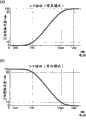
如图5(a)所示,在对于处于透射率为“0”的初始状态(施加电压为0)的液晶元件施加与白等级相当的例如5伏特的电压时,液晶元件的透射率(即液晶分子的取向状态),如图5的(b)所示,不立即变化,而是在时间上延迟而变化。在此,在将透射率从0%变化到100%所需要的响应时间设为Tr时,如果关于从置位电压的施加到基于图像信号的电压的施加为止的时间ΔT,以成为大于等于响应时间Tr的方式进行设定,则通过置位电压的施加而透射率变化为100%的状态会在超过了响应时间Tr的期间内持续存在,从而因置位电压的施加引起的透射率的变化容易被用户感知到。As shown in FIG. 5( a), when a voltage of, for example, 5 volts corresponding to a white level is applied to a liquid crystal element in an initial state (applied voltage is 0) with a transmittance of "0", the transmittance of the liquid crystal element (i.e. The alignment state of the liquid crystal molecules), as shown in (b) of FIG. 5 , does not change immediately, but changes with a time delay. Here, when Tr is the response time required for the transmittance to change from 0% to 100%, if the time ΔT from the application of the set voltage to the application of the voltage based on the image signal is equal to or greater than the response If the time Tr is set, the state in which the transmittance changes to 100% by the application of the set voltage continues for a period exceeding the response time Tr, so that the change in the transmittance caused by the application of the set voltage easily perceived by users.
因此,为了使因置位电压的施加引起的透射率的变化难以被用户感知到,可以关于时间ΔT,设定得比响应时间Tr短。Therefore, the time ΔT may be set to be shorter than the response time Tr in order to make it difficult for the user to perceive a change in transmittance due to the application of the set voltage.
如果关于响应时间进一步进行研究,则判断出:如图6所示,从初始状态、即由于施加电压为0所以仅由取向膜规定液晶分子的取向的状态,直到液晶分子开始活动(透射率开始变化)为止,需要1毫秒左右的时间。如果反过来说,则如果从施加5伏特的电压开始处于1毫秒的时间内,则透射率几乎不变化。If the response time is further studied, it is judged that as shown in Figure 6, from the initial state, that is, the state in which the orientation of the liquid crystal molecules is only defined by the alignment film because the applied voltage is 0, until the liquid crystal molecules start to move (transmittance starts Change), it takes about 1 millisecond. On the other hand, the transmittance hardly changes within 1 millisecond from the application of a voltage of 5 volts.
因此,如果关于时间ΔT设定为小于等于1毫秒,则由于在通过置位电压的施加而透射率几乎不变化的状态下施加基于图像信号的电压,所以也可以不产生因置位电压的施加引起的透射率变化。Therefore, if the time ΔT is set to be equal to or less than 1 millisecond, since the voltage based on the image signal is applied in a state where the transmittance is hardly changed by the application of the set voltage, it is also possible not to generate an error due to the application of the set voltage. caused by changes in transmittance.
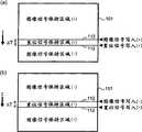
接着,关于在本实施方式中,用于对于液晶元件施加置位电压并且从该施加开始经过了时间ΔT之后施加基于图像信号的电压的结构,特别地关于转换电路30、扫描线驱动电路130以及数据线驱动电路140进行说明。Next, regarding the configuration for applying a set voltage to the liquid crystal element in this embodiment and applying a voltage based on an image signal after a time ΔT has elapsed from the application, particularly the
首先,关于转换电路30进行说明。图3是表示转换电路30的结构的图。First, the
如该图所示,转换电路30具有选择器32以及D/A转换电路34。As shown in the figure, the
其中,选择器32,按照扫描控制电路20的控制选择输入端a、b、c之中的某一个,从输出端Out输出为图像信号Vid-out。详细地,在选择器32中,在输入端a上被提供指定置位信号的信号Vst,在输入端b上被提供指定预充电信号的信号Vpr,在输入端c上被提供图像信号Vid-in。Wherein, the
由同步信号Sync规定的水平扫描期间(H)分为水平回扫期间(Hb)和水平有效扫描期间(Ha)。其中,关于水平回扫期间(Hb),在本实施方式中,如图7所示,在时间上划分为前侧的置位期间(Hs)和后侧的预充电期间(Hp)而使用。The horizontal scanning period (H) specified by the synchronization signal Sync is divided into a horizontal blanking period (Hb) and a horizontal active scanning period (Ha). However, in this embodiment, the horizontal retrace period (Hb) is temporally divided into a front set period (Hs) and a rear precharge period (Hp) as shown in FIG. 7 and used.
对于选择器32,由扫描控制电路20以分别在置位期间(Hs)选择输入端a、在预充电期间(Hp)选择输入端b、在水平有效扫描期间(Ha)选择输入端c的方式进行控制。For the
D/A转换电路34将图像信号Vid-out转换为由扫描控制电路20指定的极性的模拟的数据信号Vx。The D/
为了防止对液晶105施加直流分量,数据信号Vx的电压,例如按每一垂直扫描期间交替地切换为相对于作为视频振幅中心的电压Vcnt高位侧的正极性电压和低位侧的负极性电压。In order to prevent a DC component from being applied to the liquid crystal 105, the voltage of the data signal Vx is alternately switched between a positive polarity voltage on the high side and a negative polarity voltage on the low side with respect to the voltage Vcnt which is the center of the video amplitude, for example, every vertical scanning period.
而且,对共用电极108施加的电压LCcom也可以认为是与电压Vcnt大致相同的电压。但是,考虑到n沟道型的TFT116的截止泄漏等,对其进行调整,使其与电压Vcnt相比成为低位。Furthermore, the voltage LCcom applied to the common electrode 108 can also be considered to be substantially the same voltage as the voltage Vcnt. However, in consideration of the off-leakage of the n-channel type TFT 116 and the like, it is adjusted to be lower than the voltage Vcnt.
扫描线驱动电路130,按照扫描控制电路20的控制信号Yctr,对第1、2、3、...、m行的扫描线112供给扫描信号Y1、Y2、Y3、...、Ym。The scanning line drive circuit 130 supplies scanning signals Y1 , Y2 , Y3 , . . . , Ym to the
详细地,扫描线驱动电路130,如图7所示,以第1、2、3、...、m行这样的顺序,为了图像信号的写入而在水平有效扫描期间(Ha)选择扫描线112,并将针对所选择的扫描线的扫描信号设定为选择电压VH(H电平)。如果换言之,则扫描线驱动电路130,能够将设有水平回扫期间(Hb)这样的间隔的水平有效扫描期间(Ha),作为用于图像信号的写入的图像写入期间而施加选择电压。In detail, the scanning line driving circuit 130, as shown in FIG. 7, selects and scans in the horizontal effective scanning period (Ha) for writing an image signal in the order of the 1st, 2nd, 3rd, ..., m rows.
进而,扫描线驱动电路130,关于扫描信号Y1、Y2、Y3、...、Ym的各个,在比为了图像信号的写入而将其设定为H电平的定时提前时间ΔT的置位期间(Hs),为了置位信号的写入而将其设定为H电平。Furthermore, the scanning line driving circuit 130 sets the scanning signals Y1, Y2, Y3, . During the period (Hs), the H level is set for writing the set signal.
在此例如,如果着眼于某一行扫描线,则扫描线驱动电路130,能够在水平回扫期间(Hb)中所包含的置位期间(Hs)施加选择电压,所述水平回扫期间(Hb)中所包含的置位期间(Hs)比在水平有效扫描期间(Ha)施加选择电压的定时提前时间ΔT。此外,例如当在提供第1行的图像信号Vid-in的水平有效扫描期间(Ha)扫描信号Y1成为H电平时,在该水平扫描期间(H)的置位期间(Hs),与第1行相比处于下方p行的扫描信号Y(1+p)成为H电平。关于p,由上述时间ΔT决定。Here, for example, focusing on a certain row of scanning lines, the scanning line driving circuit 130 can apply a selection voltage during the set period (Hs) included in the horizontal retrace period (Hb). ) The set period (Hs) included in ) is advanced by time ΔT from the timing of applying the selection voltage during the horizontal active scanning period (Ha). In addition, for example, when the scanning signal Y1 becomes H level during the horizontal effective scanning period (Ha) in which the image signal Vid-in of the first line is supplied, during the set period (Hs) of the horizontal scanning period (H), the first The scan signal Y(1+p) of the p rows below the row becomes H level. Regarding p, it is determined by the above-mentioned time ΔT.
而且,扫描线驱动电路130,在为了置位信号以及图像信号的写入而设定为H电平以外的期间,将扫描信号设定为非选择电压VL(L电平)。此外,在图7中,(V)是垂直扫描期间,分为垂直有效扫描期间(Va)和垂直回扫期间(Vb)。Furthermore, the scanning line driving circuit 130 sets the scanning signal to the non-selection voltage VL (L level) during the period other than the H level for writing the set signal and the image signal. In addition, in FIG. 7 , (V) is a vertical scanning period, which is divided into a vertical effective scanning period (Va) and a vertical retrace period (Vb).
此外,在本说明书中,关于扫描信号和/或数据信号的电压,以图示省略了的接地电位作为电压0的基准。但是,关于液晶元件120的施加电压,成为共用电极108的电压LCcom与像素电极118的电位差。In addition, in this specification, regarding the voltage of the scan signal and/or the data signal, the ground potential which is not shown in the illustration is used as the reference of the
数据线驱动电路140按照扫描控制电路20的控制信号Xctr对第1~n列的数据线114提供从转换电路30提供的数据信号Vx,作为数据信号X1~Xn。详细地,数据线驱动电路140,在水平回扫期间(Hb),将基于置位信号或预充电信号的数据信号Vx一起提供给第1~n列的数据线114,在水平有效扫描期间(Ha),依次将第1列到第n列的数据信号Vx采样到第1~n列的数据线114。The data line driving circuit 140 supplies the data signal Vx supplied from the
接着,关于液晶显示装置1的工作进行说明。Next, the operation of the liquid
首先,关于提供某行(为了方便而设为i行)的图像信号Vid-in的水平扫描期间(H)的工作,参照图8进行说明。First, the operation of the horizontal scanning period (H) in which the video signal Vid-in of a certain line (for convenience, i line) is supplied will be described with reference to FIG. 8 .
在水平扫描期间(H)的水平回扫期间(Hb)之中的、在时间上处于前侧的置位期间(Hs),选择器32选择输入端a。因此,从选择器32输出的图像信号Vid-out成为指定置位信号的信号Vst,其由D/A转换电路34转换为例如正极性的电压Vw(+),作为数据信号Vx而输出。而且,电压Vw(+)是相当于正极性的白等级的数据信号,其是在被施加到液晶元件120的像素电极118时、使该液晶元件120的施加电压成为大于等于光学的饱和阈值Vsat的电压的一例。The
在置位期间(Hs),数据线驱动电路140将电压Vwt(+)的数据信号Vx一起提供给1~n列的数据线114。During the set period (Hs), the data line driving circuit 140 supplies the data signal Vx of the voltage Vwt(+) to the data lines 114 of 1˜n columns together.
另一方面,在提供第i行的图像信号Vid-in的水平扫描期间(H)之中的水平有效扫描期间(Ha),扫描信号Yi成为H电平,但是在其之前的置位期间(Hs),与第i行相比处于下方p行的扫描信号Y(i+p)成为H电平。On the other hand, during the horizontal effective scanning period (Ha) of the horizontal scanning period (H) in which the image signal Vid-in of the i-th row is supplied, the scanning signal Yi is at the H level, but in the previous set period ( Hs), the scanning signal Y(i+p) of the p rows below the i-th row becomes H level.
如果扫描信号Y(i+p)是H电平,则由于第(i+p)行的TFT116成为导通状态,所以被采样到数据线114的电压Vwt(+)的数据信号,经由处于导通状态的TFT116施加到像素电极118。由此,在(i+p)行1列~(i+p)行n列的液晶元件中,对像素电极118,作为高位侧施加相当于电压Vwt(+)与电压LCcom之差的置位电压。If the scan signal Y(i+p) is at the H level, since the TFT 116 in the (i+p)th row is turned on, the data signal sampled to the voltage Vwt(+) of the data line 114 is passed through the conduction state. The on-state TFT 116 is applied to the pixel electrode 118 . Thus, in the liquid crystal elements of (i+p)
在水平回扫期间(Hb),在置位期间(Hs)之后,成为在时间上处于后侧的预充电期间(Hp)。在预充电期间(Hp),选择器32选择输入端b。因此,从选择器32输出的图像信号Vid-out,成为指定预充电电压的信号Vpr,其由D/A转换电路34转换为例如正极性的预充电电压,作为数据信号Vx而输出。而且,在本实施方式中,作为正极性的预充电电压,使用相当于白等级的电压Vwt(+)与相当于正极性的黑等级的电压bk(+)之间的电压。In the horizontal blank period (Hb), after the set period (Hs), there is a precharge period (Hp) which is temporally behind. During the precharge period (Hp), the
在预充电期间(Hp),数据线驱动电路140将数据信号Vx一起提供给1~n列的数据线114。由此,对1~n列的数据线114,预充电为数据信号Vx的电压。而且,在预充电期间(Hp),由于扫描信号Y1~Yn均是L电平,所以全部的TFT116成为截止状态。因此,在预充电期间(Hp),液晶元件120的施加电压不发生变化。During the precharge period (Hp), the data line driving circuit 140 supplies the data signal Vx to the data lines 114 of
在预充电期间(Hp)之后,成为水平有效扫描期间(Ha)。由于在水平有效扫描期间(Ha),选择器32选择输入端c,所以图像信号Vid-out等于图像信号Vid-in。在第i行的水平有效扫描期间(Ha),图像信号Vid-in(Vid-out)依次规定i行1列、i行2列、i行3列、...、i行n列的像素的灰度等级。如图8所示,图像信号Vid-out,由D/A转换电路34在此转换为正极性的数据信号Vx,并且由数据线驱动电路140作为数据信号X1~Xn依次采样到第1~n列的数据线114。例如,与i行3列对应的数据信号Vx作为数据信号X3被采样到第3列的数据线114。After the precharge period (Hp), it becomes a horizontal active scanning period (Ha). Since the
在第i行的水平有效扫描期间(Ha),由于扫描线信号Yi成为H电平,所以第i行的TFT116成为导通状态。因此,被采样到数据线114的数据信号,经由处于导通状态的TFT116施加到像素电极118。由此,在i行1列~i行n列的液晶元件中,对像素电极118,作为高位侧施加相当于数据信号与电压LCcom之差的电压、即与灰度等级相应的电压。In the horizontal effective scanning period (Ha) of the i-th row, since the scanning line signal Yi is at H level, the TFTs 116 in the i-th row are turned on. Therefore, the data signal sampled on the data line 114 is applied to the pixel electrode 118 via the TFT 116 in the on state. Thus, in the liquid crystal elements of i row 1 column to i row n column, a voltage corresponding to the difference between the data signal and the voltage LCcom, that is, a voltage corresponding to the gray scale is applied to the pixel electrode 118 as the upper side.
而且,在本实施方式中,由于采用常黑模式,所以图8中的数据信号Vx的电压波形,如果是正极性,则其相对于基准电压Vcnt,随着所指定的灰度等级变明亮而成为高位侧的电压;如果是负极性,则其相对于基准电压Vcnt,随着灰度等级变明亮而成为低位侧的电压。Moreover, in this embodiment, since the normally black mode is adopted, if the voltage waveform of the data signal Vx in FIG. It becomes a voltage on the high side; if it is negative, it becomes a voltage on the low side as the gray scale becomes brighter with respect to the reference voltage Vcnt.
详细地,如果数据信号Vx的电压是正极性,则其在从相当于白色的电压Vw(+)到相当于黑色的电压Vb(+)的范围内,成为从基准电压Vcnt偏离了与灰度等级相应的量的电压;另一方面,如果数据信号Vx的电压是负极性,则其在从相当于白色的电压Vw(-)到相当于黑色的电压Vb(-)的范围内,成为从基准电压Vcnt偏离了与灰度等级相应的量的电压。In detail, if the voltage of the data signal Vx is positive, it becomes a gray scale deviated from the reference voltage Vcnt in the range from the voltage Vw(+) corresponding to white to the voltage Vb(+) corresponding to black. On the other hand, if the voltage of the data signal Vx is negative, it becomes from the voltage Vw(-) corresponding to white to the voltage Vb(-) corresponding to black. The reference voltage Vcnt deviates from the voltage by the amount corresponding to the gray scale.
而且,电压Vw(+)与电压Vw(-)处于以电压Vcnt为中心相互对称的关系。关于电压Vb(+)与Vb(-),也处于以电压Vcnt为中心相互对称的关系。Furthermore, the voltage Vw(+) and the voltage Vw(-) are in a mutually symmetrical relationship around the voltage Vcnt. The voltages Vb(+) and Vb(-) are also in a mutually symmetrical relationship around the voltage Vcnt.
在此,如果基准电压Vcnt与电压LCcom相一致,则对液晶元件施加数据信号的电压与电压LCcom之差。Here, when the reference voltage Vcnt matches the voltage LCcom, the difference between the voltage of the data signal and the voltage LCcom is applied to the liquid crystal element.
以上,是关于提供第i行的图像信号Vid-in的水平扫描期间(H)的工作。The above is about the operation of the horizontal scanning period (H) in which the image signal Vid-in of the i-th row is supplied.
图像信号Vid-in实际上以第1、2、3、4、...、(m-1)、m行的顺序提供,另一方面,如图7所示,在提供该图像信号Vid-in的整个垂直有效扫描期间(Va),扫描信号Y1、Y2、Y3、Y4、...、Y(m-1)、Ym依次在水平有效扫描期间(Ha)成为H电平。由此,对第1、2、3、4、...、(m-1)、m行的各个液晶元件,分别施加与图像信号Vid-in相应的电压。The image signal Vid-in is actually provided in the order of the 1st, 2nd, 3rd, 4th, ..., (m-1), m rows. On the other hand, as shown in FIG. 7, when the image signal Vid-in is provided During the entire vertical effective scanning period (Va) of in, the scanning signals Y1, Y2, Y3, Y4, . Thus, voltages corresponding to the image signal Vid-in are applied to the respective liquid crystal elements in the first, second, third, fourth, . . . , (m−1), and m rows.
进而,在比水平有效扫描期间(Ha)中扫描信号Y1、Y2、...、Y(m-1)、Ym分别依次成为H电平的期间提前时间ΔT的置位期间(Hs),扫描信号Y1、Y2、...、Y(m-1)、Ym也分别依次成为H电平。由此,在第1、2、...、(m-1)、m行的各个液晶元件中,由于分别施加与置位信号相应的置位电压,所以液晶分子活动,从而摆脱受横电场的影响的状态。Furthermore, in the set period (Hs) which is earlier than the period in which the scanning signals Y1, Y2, . Signals Y1 , Y2 , . . . , Y(m−1), Ym also attain H level sequentially. Therefore, in each liquid crystal element in the 1st, 2nd, ..., (m-1), m rows, since the set voltage corresponding to the set signal is respectively applied, the liquid crystal molecules move, thereby getting rid of the transverse electric field status of the impact.
而且,在本实施方式中,置位期间中的置位信号的极性与时间ΔT后的与图像信号相应的数据信号的极性相同。虽然第1、2、3、...、(p-1)行的置位期间(Hs)分别属于前1个垂直扫描期间(V),但是扫描控制电路20对D/A转换电路34指定为,关于置位信号的极性,与经过了时间ΔT时的水平有效扫描期间(Ha)中的数据信号的极性一致。Furthermore, in the present embodiment, the polarity of the set signal in the set period is the same as the polarity of the data signal corresponding to the image signal after time ΔT. Although the set periods (Hs) of the 1st, 2nd, 3rd, ..., (p-1) rows respectively belong to the previous vertical scanning period (V), the scanning control circuit 20 specifies to the D/
关于各行的液晶元件,如果以时间经过的顺序,则在置位信号的写入之后,在经过了时间ΔT的时刻写入与图像信号相应的电压。With respect to the liquid crystal elements in each row, in the order of time, a voltage corresponding to an image signal is written at the time ΔT has elapsed after the writing of the set signal.
图9(a)以及(b)表示了该写入的推进与显示区域101的关系。其中,图9(a)表示以正极性写入基于图像信号的数据信号的情况。9( a ) and ( b ) show the relationship between the progress of writing and the
在此情况下,如果为了写入正极性的置位信号而在置位期间(Hs)选择扫描线112,则在继该置位期间之后的水平有效扫描期间(Ha)选择相对于该扫描线处于上方p行的扫描线112,写入正极性的数据信号。所选择的扫描线均保持p行的间隔而从上朝向下方推进。In this case, if the
而且,选择扫描线的下侧区域,是改写之前、即通过之前的选择而写入的信号的保持区域,选择扫描线的上侧区域是通过选择而改写了的信号的保持区域。此外,在图中,为了写入置位信号而选择的扫描线112,在经过时间ΔT后,为了写入图像信号而再次被选择。Also, the area below the selected scanning line is a holding area for signals written before rewriting, that is, by previous selection, and the area above the selected scanning line is a holding area for signals rewritten by selection. In addition, in the drawing, the
图9(b)表示以负极性写入基于图像信号的数据信号的情况,表示了如果为了写入负极性的置位信号而选择扫描线112,则选择相对于该扫描线处于上方p行的扫描线112,写入负极性的数据信号。Figure 9(b) shows the case of writing a data signal based on an image signal with a negative polarity, and shows that if the
这样,在本实施方式中,各液晶元件,即使当在之前的垂直扫描期间中施加与图像信号相应的电压时受到横电场的影响,也由于液晶分子通过置位电压的施加而活动,所以可摆脱受横电场的影响的状态。并且,在该摆脱之后的状态下在接着的垂直扫描期间对液晶元件施加与图像信号相应的电压。因此,在本实施方式中,可以抑制因反向倾斜域引起的显示上的不良状况的产生。Thus, in this embodiment, each liquid crystal element is affected by a transverse electric field when a voltage corresponding to an image signal is applied in the previous vertical scanning period, since the liquid crystal molecules are moved by the application of the set voltage, it can be Get rid of the state affected by the transverse electric field. Then, a voltage corresponding to the image signal is applied to the liquid crystal element in the subsequent vertical scanning period in the state after the release. Therefore, in the present embodiment, it is possible to suppress the occurrence of display defects due to the reverse slope domain.
此外,在本实施方式中,由于不需要改变液晶面板100的结构,所以也不会引起开口率的下降,此外,也可以应用于未改进结构而已经制作的液晶面板。In addition, in this embodiment, since the structure of the
此外,在本实施方式中,由于不是对于特定的像素,而是与应当显示的图像无关地一律施加置位电压,并且将相当于置位电压的保持期间的时间ΔT设定得比响应时间Tr短,所以可以使因置位电压引起的透射率的变化和/或违反显示的状态(即显示不基于图像信号的图像的状态)几乎不被用户感知到。In addition, in this embodiment, since the set voltage is applied uniformly regardless of the image to be displayed, not to a specific pixel, the time ΔT corresponding to the holding period of the set voltage is set to be longer than the response time Tr Short, so that the change in transmittance due to the set voltage and/or the state of violating the display (ie, the state of displaying an image not based on the image signal) can be hardly perceived by the user.
此外,由于不需要对图像信号Vid-in进行分析,所以也能够防止电路结构复杂化的情况。In addition, since it is not necessary to analyze the video signal Vid-in, it is also possible to prevent the circuit configuration from becoming complicated.
进而,在本实施方式中,由于使置位期间中的置位信号的极性与时间ΔT后的与图像信号相应的数据信号的极性相同,所以即将写入与图像信号相应的数据信号之前的状态与施加了置位电压后的状态一致。因此,可以保持由交流驱动实现的极性的平衡,并且可以进行均匀的写入。进而,由于置位电压是大于等于光学的饱和电压Vsat的高电压,所以可以使与图像信号相应的数据信号的写入其成为响应快的放电方向的写入的概率提高,从而充分地写入与图像信号相应的数据信号。特别地,在本实施方式中,由于将置位信号设定为常黑模式中最高的白等级的电压,所以能够使与图像信号相应的数据信号的写入,除了成为白等级的情况之外,必定成为放电方向的写入。Furthermore, in this embodiment, since the polarity of the set signal in the set period is made the same as the polarity of the data signal corresponding to the image signal after time ΔT, immediately before writing the data signal corresponding to the image signal The state is the same as the state after the set voltage is applied. Therefore, the polarity balance achieved by AC driving can be maintained, and uniform writing can be performed. Furthermore, since the set voltage is a high voltage equal to or greater than the optical saturation voltage Vsat, it is possible to increase the probability that the writing of the data signal corresponding to the image signal will be writing in the discharge direction with a fast response, thereby sufficiently writing A data signal corresponding to an image signal. In particular, in this embodiment, since the set signal is set to the voltage of the highest white level in the normally black mode, it is possible to write data signals corresponding to image signals, except for the case of white level , must be writing in the discharge direction.
本发明并不限于上述的实施方式,而可以实现各种应用、变形。The present invention is not limited to the above-described embodiments, and various applications and modifications are possible.
例如,也可以应用于特开2004-177930号公报中所记载的区域扫描方式,详细地,如第1、(m/2+1)、2、(m/2+2)、3、(m/2+3)、4、(m/2+4)、...行那样,以跳过m行的一半数量的扫描线的顺序进行选择,并且,其中,例如通过第1、2、3、...行的选择而以正极性写入基于图像信号的数据信号,通过(m/2+1)、(m/2+2)、(m/2+3)、...行的选择而以负极性写入基于该图像信号的数据信号的技术。For example, it can also be applied to the area scanning method described in JP-A-2004-177930. Specifically, as in the first, (m/2+1), 2, (m/2+2), 3, (m /2+3), 4, (m/2+4), ... lines, the selection is performed in the order of skipping half the scan lines of m lines, and, for example, by the 1st, 2nd, 3rd lines , ... the selection of the row and write the data signal based on the image signal with positive polarity, through the (m/2+1), (m/2+2), (m/2+3), ... row A technique for writing a data signal based on the image signal with a negative polarity is selected.
例如也可以如图10所示,成为以下结构:在为了写入将图像信号转换为正极性所得到的数据信号而选择扫描线112时,在比该选择提前时间ΔT之时,选择该扫描线112而写入正极性的置位信号,另一方面,在为了写入将图像信号转换为负极性所得到的数据信号而选择扫描线112时,在比该选择提前时间ΔT之时,选择该扫描线112而写入负极性的置位信号。For example, as shown in FIG. 10, a configuration may be adopted in which, when the
利用该结构,能够抑制串扰,并且,可以在确保画面内的均匀性的基础上,抑制因反向倾斜域引起的显示上的不良状况的产生。With this configuration, crosstalk can be suppressed, and the occurrence of display defects due to the reverse tilt domain can be suppressed while ensuring uniformity within the screen.
如果如上所述关于时间ΔT设定为小于等于1毫秒,则几乎不会产生因置位电压的施加引起的透射率变化。但是,如果将时间ΔT设定为接近于响应时间Tr的值,则如果是常黑模式,被施加了置位电压的液晶元件的透射率最终将接近于100%(参照图5的(b))。因此,有可能产生画面的整体变明亮(白)的白化现象。If the time ΔT is set to be equal to or less than 1 millisecond as described above, almost no change in transmittance due to application of the set voltage occurs. However, if the time ΔT is set to a value close to the response time Tr, then in the normally black mode, the transmittance of the liquid crystal element to which the set voltage is applied will eventually approach 100% (see (b) of FIG. ). Therefore, there is a possibility of occurrence of a whitening phenomenon in which the entire screen becomes bright (white).
另一方面,如果构成为使施加置位电压的液晶元件的比例从100%下降、不施加置位电压而代之对液晶元件施加暗的灰度等级的电压,则虽然能够使白化现象的程度下降,但是如果不考虑排列而使比例下降,则将不能够期待抑制反向倾斜域的产生的原本的效果。On the other hand, if the ratio of the liquid crystal element to which the set voltage is applied is reduced from 100%, and instead of applying the set voltage, a dark grayscale voltage is applied to the liquid crystal element, although the degree of the whitening phenomenon can be reduced However, if the ratio is lowered regardless of the alignment, the original effect of suppressing the occurrence of the reverse tilt domain cannot be expected.
在此,即使是不被施加置位电压的液晶元件,如果与被施加了置位电压的(即液晶分子活动了的)状态的液晶元件相邻,则也难以受横电场的影响。因此,例如,也可以如图11的(a)所示成为使施加置位电压的液晶元件(像素)每隔1列的结构,详细地,成为以下结构:数据线驱动电路140在置位期间(Hs),例如仅对奇数列的数据线施加置位信号,关于偶数列的数据线,施加截止信号(即常黑模式中使像素变暗的数据信号)。Here, even a liquid crystal element to which a set voltage is not applied is less likely to be affected by a transverse electric field if it is adjacent to a liquid crystal element to which a set voltage is applied (that is, in which liquid crystal molecules are moving). Therefore, for example, as shown in (a) of FIG. 11 , a structure in which the liquid crystal elements (pixels) to which the set voltage is applied is every other column may be adopted. Specifically, the structure in which the data line driving circuit 140 (Hs), for example, a set signal is applied only to the data lines of the odd columns, and an off signal (ie, a data signal for darkening the pixels in the normally black mode) is applied to the data lines of the even columns.
此外,也可以如图11的(b)所示,成为使施加置位电压的像素每隔1行的结构,详细地,成为以下结构:数据线驱动电路140,当在置位期间(Hs)例如奇数行的扫描线被选择时对1~n列的数据线提供置位信号,当在置位期间(Hs)偶数行的扫描线被选择时对1~n列的数据线提供截止信号。In addition, as shown in (b) of FIG. 11 , a structure in which pixels to which set voltages are applied every other row may be adopted. Specifically, the following structure is adopted: when the data line driving circuit 140 is in the set period (Hs) For example, when the scan lines of odd rows are selected, set signals are provided to the data lines of 1-n columns, and when the scan lines of even-numbered rows are selected during the set period (Hs), an off signal is provided to the data lines of 1-n columns.
或者,也可以如图11的(c)所示,成为使图11的(a)与(b)组合、使施加置位电压的像素成为每隔1像素的方格花纹的结构,详细地,成为以下结构:数据线驱动电路140,当在置位期间(Hs)例如奇数行的扫描线被选择时对奇数列的数据线提供置位信号,对偶数列的数据线提供截止信号,并且当在置位期间(Hs)偶数行的扫描线被选择时对奇数列的数据线提供截止信号,对偶数列的数据线提供置位信号。Alternatively, as shown in (c) of FIG. 11, a combination of (a) and (b) of FIG. 11 may be used to make the pixels to which the set voltage is applied have a checkered pattern every other pixel. In detail, It becomes the following structure: the data line driving circuit 140 provides a set signal to the data lines of the odd columns when, for example, the scan lines of the odd rows are selected during the set period (Hs), and provides a cut-off signal to the data lines of the even columns, and when During the set period (Hs), when the scan lines of the even rows are selected, an off signal is provided to the data lines of the odd columns, and a set signal is provided to the data lines of the even columns.
根据这三个结构,都是即使在将时间ΔT设定为接近于响应时间Tr的值时,也可以兼顾常黑模式的白化现象的抑制与反向倾斜域的减少。According to these three configurations, even when the time ΔT is set to a value close to the response time Tr, both the suppression of the whitening phenomenon in the normally black mode and the reduction of the reverse tilt region can be achieved.
而且,当然也可以将图11的(a)、(b)或(c)应用于图10所示的区域扫描方式。Furthermore, it is of course possible to apply (a), (b) or (c) of FIG. 11 to the area scanning method shown in FIG. 10 .
在各实施方式中,液晶元件120并不限于透射型,而也可以是反射型的。进而,液晶元件120并不限于常黑模式,而也可以设定为作为例如TN方式、液晶元件120在无电压施加时成为白状态的常白模式。在设定为常白模式时,液晶元件120的施加电压与透射率(反射率)的关系,由图4的(b)所示的V-T特性表示,随着施加电压变高而透射率减小。此外,在设定为常白模式时,液晶元件120的响应特性成为图5的(c)所示的特性。In each embodiment, the liquid crystal element 120 is not limited to a transmissive type, but may be a reflective type. Furthermore, the liquid crystal element 120 is not limited to the normally black mode, but may be set to a normally white mode in which the liquid crystal element 120 is in a white state when no voltage is applied, for example, as a TN system. When the normally white mode is set, the relationship between the applied voltage and the transmittance (reflectance) of the liquid crystal element 120 is represented by the V-T characteristic shown in (b) of FIG. 4 , and the transmittance decreases as the applied voltage increases. . In addition, when the normally white mode is set, the response characteristics of the liquid crystal element 120 become the characteristics shown in (c) of FIG. 5 .
而且,常黑模式中的白化现象,在设定为常白模式时,成为黑化现象。由于截止信号为使像素变明亮的数据信号,所以如果采用图11的(a)~(c),则可以减轻黑化现象。Furthermore, the whitening phenomenon in the normally black mode becomes a blackening phenomenon when the normally white mode is set. Since the OFF signal is a data signal for brightening a pixel, the blackening phenomenon can be reduced by using (a) to (c) of FIG. 11 .
<电子设备><electronic device>
接着,作为使用了上述的实施方式的液晶显示装置的电子设备的一例,关于将液晶面板100用作为光阀的投影型显示装置(投影机)进行说明。图12是表示该投影机的结构的俯视图。Next, a projection type display device (projector) using the
如该图所示,在投影机2100的内部,设置有由卤素灯等白色光源构成的灯单元2102。从该灯单源2102射出的投影光由在内部配置的3块镜2106以及2块分色镜2108分离为R(红)色、G(绿)色、B(蓝)色这3原色,并分别被引导至与各原色对应的光阀100R、100G以及100B。而且,B色的光,如果与其他的R色和/或G色比较,则光路长,所以为了防止其损失,经过由入射透镜2122、中继透镜2123以及射出透镜2124构成的中继透镜系统2121对其进行引导。As shown in the figure, inside the projector 2100, a lamp unit 2102 composed of a white light source such as a halogen lamp is provided. Projection light emitted from the lamp single source 2102 is separated into three primary colors of R (red), G (green) and B (blue) by three mirrors 2106 and two dichroic mirrors 2108 arranged inside, and They are respectively guided to light valves 100R, 100G, and 100B corresponding to the respective primary colors. And, the light of B color, if compare with other R color and/or G color, then the optical path is long, so in order to prevent its loss, pass through the relay lens system that is made up of incident lens 2122, relay lens 2123 and exit lens 2124 2121 to guide it.
在该投影机2100中,包含液晶面板100的液晶显示装置与R色、G色、B色分别对应而设置3组。光阀100R、100G以及100B的结构与上述的液晶面板100相同。成为为了指定R色、G色、B色这各个原色分量的灰度等级,图像信号分别从外部上位电路被提供而分别驱动光阀100R、100G以及100B的结构。由光阀100R、100G、100B分别调制后的光,从3个方向入射到分色棱镜2112。并且,在该分色棱镜2112中,R色以及B色的光曲折90度,另一方面,G色的光直线前进。因而,各原色的图像被合成之后,在屏幕2120上,由投影透镜组2114投影彩色图像。In this projector 2100, three sets of liquid crystal display devices including the
而且,由于在光阀100R、100G以及100B上,通过分色镜2108入射分别与R色、G色、B色对应的光,所以不需要设置滤色器。此外,由于光阀100R、100B的透射像在由分色棱镜2112反射后被投影,相对于此,光阀100G的透射像原样被投影,所以成为光阀100R、100B的水平扫描方向与光阀100G的水平扫描方向成为相反方向而显示使左右反转了的像的结构。Furthermore, since the light corresponding to the R color, the G color, and the B color respectively enters the light valves 100R, 100G, and 100B through the dichroic mirror 2108 , no color filter is required. In addition, since the transmitted images of the light valves 100R and 100B are projected after being reflected by the dichroic prism 2112, the transmitted images of the light valve 100G are projected as they are, so the horizontal scanning direction of the light valves 100R and 100B is the same as that of the light valve. The horizontal scanning direction of 100G is reversed to display a left-right inverted image.
作为电子设备,除了参照图12说明的投影机外,还可以列举电视机、取景器型/监视器直视型的录像机、汽车导航装置、寻呼机、电子记事簿、电子计算器、文字处理机、工作站、电视电话、POS终端、数字照相机、移动电话机、具备触摸面板的设备等。并且,对于这各种电子设备,当然可以应用上述液晶显示装置。As electronic equipment, in addition to the projector described with reference to FIG. Workstations, TV phones, POS terminals, digital cameras, mobile phones, devices with touch panels, etc. And, of course, the above-mentioned liquid crystal display device can be applied to these various electronic devices.
Claims (9)
Translated fromChineseApplications Claiming Priority (2)
| Application Number | Priority Date | Filing Date | Title |
|---|---|---|---|
| JP2009205682AJP5370021B2 (en) | 2009-09-07 | 2009-09-07 | Liquid crystal display device, driving method, and electronic apparatus |
| JP205682/2009 | 2009-09-07 |
Publications (1)
| Publication Number | Publication Date |
|---|---|
| CN102013240Atrue CN102013240A (en) | 2011-04-13 |
Family
ID=43647496
Family Applications (1)
| Application Number | Title | Priority Date | Filing Date |
|---|---|---|---|
| CN2010102775092APendingCN102013240A (en) | 2009-09-07 | 2010-09-07 | Liquid crystal display device, driving method and electronic device |
Country Status (3)
| Country | Link |
|---|---|
| US (1) | US20110058111A1 (en) |
| JP (1) | JP5370021B2 (en) |
| CN (1) | CN102013240A (en) |
Families Citing this family (4)
| Publication number | Priority date | Publication date | Assignee | Title |
|---|---|---|---|---|
| JP5556234B2 (en) | 2010-02-25 | 2014-07-23 | セイコーエプソン株式会社 | VIDEO PROCESSING CIRCUIT, ITS PROCESSING METHOD, LIQUID CRYSTAL DISPLAY DEVICE, AND ELECTRONIC DEVICE |
| JP5720221B2 (en) | 2010-12-13 | 2015-05-20 | セイコーエプソン株式会社 | Video processing method, video processing circuit, liquid crystal display device, and electronic apparatus |
| JP5635480B2 (en) | 2011-11-22 | 2014-12-03 | 株式会社ジャパンディスプレイ | Display device with touch sensor, potential control method, and program |
| JP6078959B2 (en)* | 2012-03-16 | 2017-02-15 | セイコーエプソン株式会社 | VIDEO PROCESSING CIRCUIT, VIDEO PROCESSING METHOD, AND ELECTRONIC DEVICE |
Citations (4)
| Publication number | Priority date | Publication date | Assignee | Title |
|---|---|---|---|---|
| JP2003131265A (en)* | 2001-10-23 | 2003-05-08 | Matsushita Electric Ind Co Ltd | Driving method of liquid crystal display device |
| US20040196415A1 (en)* | 2001-05-31 | 2004-10-07 | Masanori Kimura | Liquid crystal dispaly element driving method and liquid crystal display using the same |
| CN1648983A (en)* | 2004-01-28 | 2005-08-03 | 精工爱普生株式会社 | Electro-optic device, its drive circuit, drive method, and electronic device |
| CN101467200A (en)* | 2006-09-28 | 2009-06-24 | 夏普株式会社 | Liquid crystal display device, and driving circuit and driving method thereof |
Family Cites Families (15)
| Publication number | Priority date | Publication date | Assignee | Title |
|---|---|---|---|---|
| TW521241B (en)* | 1999-03-16 | 2003-02-21 | Sony Corp | Liquid crystal display apparatus, its driving method, and liquid crystal display system |
| JP4519251B2 (en)* | 1999-10-13 | 2010-08-04 | シャープ株式会社 | Liquid crystal display device and control method thereof |
| JP4894081B2 (en)* | 2000-06-14 | 2012-03-07 | ソニー株式会社 | Display device and driving method thereof |
| JP3913040B2 (en)* | 2001-11-08 | 2007-05-09 | 東芝松下ディスプレイテクノロジー株式会社 | Method for driving liquid crystal display device and liquid crystal display device |
| JP3901048B2 (en)* | 2002-07-24 | 2007-04-04 | 日本ビクター株式会社 | Active matrix liquid crystal display device |
| JP4177065B2 (en)* | 2002-10-03 | 2008-11-05 | 三菱電機株式会社 | Liquid crystal display |
| JP4628650B2 (en)* | 2003-03-17 | 2011-02-09 | 株式会社日立製作所 | Display device and driving method thereof |
| JP4239892B2 (en)* | 2003-07-14 | 2009-03-18 | セイコーエプソン株式会社 | Electro-optical device, driving method thereof, projection display device, and electronic apparatus |
| JP2006072078A (en)* | 2004-09-03 | 2006-03-16 | Mitsubishi Electric Corp | Liquid crystal display device and driving method thereof |
| JP2006106689A (en)* | 2004-09-13 | 2006-04-20 | Seiko Epson Corp | Display method for liquid crystal panel, liquid crystal display device and electronic apparatus |
| TW200629210A (en)* | 2004-11-26 | 2006-08-16 | Hitachi Displays Ltd | Liquid-crystal display device and method of driving liquid-crystal display device |
| JP4887657B2 (en)* | 2005-04-27 | 2012-02-29 | 日本電気株式会社 | Active matrix display device and driving method thereof |
| JP2008015179A (en)* | 2006-07-05 | 2008-01-24 | Toshiba Matsushita Display Technology Co Ltd | Liquid crystal display |
| JP2008268887A (en)* | 2007-03-29 | 2008-11-06 | Nec Lcd Technologies Ltd | Image display device |
| JP2008275968A (en)* | 2007-05-01 | 2008-11-13 | Epson Imaging Devices Corp | Electro-optical device, method of driving electro-optical device and electric device |
- 2009
- 2009-09-07JPJP2009205682Apatent/JP5370021B2/ennot_activeExpired - Fee Related
- 2010
- 2010-08-19USUS12/859,392patent/US20110058111A1/ennot_activeAbandoned
- 2010-09-07CNCN2010102775092Apatent/CN102013240A/enactivePending
Patent Citations (4)
| Publication number | Priority date | Publication date | Assignee | Title |
|---|---|---|---|---|
| US20040196415A1 (en)* | 2001-05-31 | 2004-10-07 | Masanori Kimura | Liquid crystal dispaly element driving method and liquid crystal display using the same |
| JP2003131265A (en)* | 2001-10-23 | 2003-05-08 | Matsushita Electric Ind Co Ltd | Driving method of liquid crystal display device |
| CN1648983A (en)* | 2004-01-28 | 2005-08-03 | 精工爱普生株式会社 | Electro-optic device, its drive circuit, drive method, and electronic device |
| CN101467200A (en)* | 2006-09-28 | 2009-06-24 | 夏普株式会社 | Liquid crystal display device, and driving circuit and driving method thereof |
Also Published As
| Publication number | Publication date |
|---|---|
| JP2011059160A (en) | 2011-03-24 |
| JP5370021B2 (en) | 2013-12-18 |
| US20110058111A1 (en) | 2011-03-10 |
Similar Documents
| Publication | Publication Date | Title |
|---|---|---|
| TWI539426B (en) | Signal processing device, signal processing method, liquid crystal display device, and electronic device therewith | |
| CN102005192B (en) | Video processing circuit, processing method thereof, liquid crystal display apparatus and electronics device | |
| CN102129849B (en) | Video processing circuit, video processing method, liquid crystal display apparatus and electronic device | |
| TWI476478B (en) | Video processing method, video processing circuit, liquid crystal display, and electronic apparatus | |
| CN102169679B (en) | Video processing circuit, video processing method, liquid crystal display device, and electronic apparatus | |
| CN102157135B (en) | Image processing circuit and processing method, liquid crystal display device, and electronic apparatus | |
| US8497829B2 (en) | Video processing circuit, liquid crystal display device, electronic apparatus, and video processing method | |
| CN102063883B (en) | Video processing circuit and method, liquid crystal display apparatus, and electronic apparatus | |
| CN102163415B (en) | Video processing circuit, video processing method, liquid crystal display device, and electronic apparatus | |
| CN101241679B (en) | Electro-optical device, driving method, and electronic apparatus | |
| JP6488651B2 (en) | Electro-optical device, control method of electro-optical device, and electronic apparatus | |
| JP4349434B2 (en) | Electro-optical device, driving circuit thereof, driving method, and electronic apparatus | |
| JP5217734B2 (en) | Electro-optical device, driving method, and electronic apparatus | |
| CN103366698A (en) | Signal processing device, liquid crystal apparatus, electronic equipment and signal processing method | |
| CN100363962C (en) | Driving method of electro-optical device, driving circuit, electro-optical device and electronic equipment | |
| JP2005148304A (en) | Electro-optical device driving method, electro-optical device, and electronic apparatus | |
| JP5370021B2 (en) | Liquid crystal display device, driving method, and electronic apparatus | |
| JP2020064103A (en) | Method for driving electro-optical device, electro-optical device, and electronic apparatus | |
| JP2010026281A (en) | Electrooptical apparatus, driving method and electronic device | |
| JP2007199418A (en) | Electro-optical device, driving method, and electronic apparatus | |
| JP5574000B2 (en) | Signal processing device, liquid crystal display device, electronic device, and signal processing method | |
| JP2014219686A (en) | Video processing circuit, processing method of the same, liquid crystal display device, and electronic apparatus | |
| JP5510580B2 (en) | Signal processing device, signal processing method, liquid crystal display device, and electronic apparatus | |
| JP2013156645A (en) | Electro-optic device, controller of electro-optic device, and electronic equipment | |
| JP2009128405A (en) | Electro-optical device, driving method thereof, and electronic apparatus |
Legal Events
| Date | Code | Title | Description |
|---|---|---|---|
| C06 | Publication | ||
| PB01 | Publication | ||
| C10 | Entry into substantive examination | ||
| SE01 | Entry into force of request for substantive examination | ||
| C02 | Deemed withdrawal of patent application after publication (patent law 2001) | ||
| WD01 | Invention patent application deemed withdrawn after publication | Application publication date:20110413 |