CN102005541A - Thin film deposition apparatus and method of manufacturing organic light-emitting display apparatus using the same - Google Patents
Thin film deposition apparatus and method of manufacturing organic light-emitting display apparatus using the sameDownload PDFInfo
- Publication number
- CN102005541A CN102005541ACN2010102664066ACN201010266406ACN102005541ACN 102005541 ACN102005541 ACN 102005541ACN 2010102664066 ACN2010102664066 ACN 2010102664066ACN 201010266406 ACN201010266406 ACN 201010266406ACN 102005541 ACN102005541 ACN 102005541A
- Authority
- CN
- China
- Prior art keywords
- deposition
- thin film
- chamber
- film deposition
- substrate
- Prior art date
- Legal status (The legal status is an assumption and is not a legal conclusion. Google has not performed a legal analysis and makes no representation as to the accuracy of the status listed.)
- Granted
Links
Images


Classifications
- C—CHEMISTRY; METALLURGY
- C23—COATING METALLIC MATERIAL; COATING MATERIAL WITH METALLIC MATERIAL; CHEMICAL SURFACE TREATMENT; DIFFUSION TREATMENT OF METALLIC MATERIAL; COATING BY VACUUM EVAPORATION, BY SPUTTERING, BY ION IMPLANTATION OR BY CHEMICAL VAPOUR DEPOSITION, IN GENERAL; INHIBITING CORROSION OF METALLIC MATERIAL OR INCRUSTATION IN GENERAL
- C23C—COATING METALLIC MATERIAL; COATING MATERIAL WITH METALLIC MATERIAL; SURFACE TREATMENT OF METALLIC MATERIAL BY DIFFUSION INTO THE SURFACE, BY CHEMICAL CONVERSION OR SUBSTITUTION; COATING BY VACUUM EVAPORATION, BY SPUTTERING, BY ION IMPLANTATION OR BY CHEMICAL VAPOUR DEPOSITION, IN GENERAL
- C23C14/00—Coating by vacuum evaporation, by sputtering or by ion implantation of the coating forming material
- C23C14/04—Coating on selected surface areas, e.g. using masks
- C23C14/042—Coating on selected surface areas, e.g. using masks using masks
- C—CHEMISTRY; METALLURGY
- C23—COATING METALLIC MATERIAL; COATING MATERIAL WITH METALLIC MATERIAL; CHEMICAL SURFACE TREATMENT; DIFFUSION TREATMENT OF METALLIC MATERIAL; COATING BY VACUUM EVAPORATION, BY SPUTTERING, BY ION IMPLANTATION OR BY CHEMICAL VAPOUR DEPOSITION, IN GENERAL; INHIBITING CORROSION OF METALLIC MATERIAL OR INCRUSTATION IN GENERAL
- C23C—COATING METALLIC MATERIAL; COATING MATERIAL WITH METALLIC MATERIAL; SURFACE TREATMENT OF METALLIC MATERIAL BY DIFFUSION INTO THE SURFACE, BY CHEMICAL CONVERSION OR SUBSTITUTION; COATING BY VACUUM EVAPORATION, BY SPUTTERING, BY ION IMPLANTATION OR BY CHEMICAL VAPOUR DEPOSITION, IN GENERAL
- C23C14/00—Coating by vacuum evaporation, by sputtering or by ion implantation of the coating forming material
- C23C14/06—Coating by vacuum evaporation, by sputtering or by ion implantation of the coating forming material characterised by the coating material
- C23C14/12—Organic material
- C—CHEMISTRY; METALLURGY
- C23—COATING METALLIC MATERIAL; COATING MATERIAL WITH METALLIC MATERIAL; CHEMICAL SURFACE TREATMENT; DIFFUSION TREATMENT OF METALLIC MATERIAL; COATING BY VACUUM EVAPORATION, BY SPUTTERING, BY ION IMPLANTATION OR BY CHEMICAL VAPOUR DEPOSITION, IN GENERAL; INHIBITING CORROSION OF METALLIC MATERIAL OR INCRUSTATION IN GENERAL
- C23C—COATING METALLIC MATERIAL; COATING MATERIAL WITH METALLIC MATERIAL; SURFACE TREATMENT OF METALLIC MATERIAL BY DIFFUSION INTO THE SURFACE, BY CHEMICAL CONVERSION OR SUBSTITUTION; COATING BY VACUUM EVAPORATION, BY SPUTTERING, BY ION IMPLANTATION OR BY CHEMICAL VAPOUR DEPOSITION, IN GENERAL
- C23C14/00—Coating by vacuum evaporation, by sputtering or by ion implantation of the coating forming material
- C23C14/22—Coating by vacuum evaporation, by sputtering or by ion implantation of the coating forming material characterised by the process of coating
- C23C14/24—Vacuum evaporation
- C23C14/243—Crucibles for source material
- C—CHEMISTRY; METALLURGY
- C23—COATING METALLIC MATERIAL; COATING MATERIAL WITH METALLIC MATERIAL; CHEMICAL SURFACE TREATMENT; DIFFUSION TREATMENT OF METALLIC MATERIAL; COATING BY VACUUM EVAPORATION, BY SPUTTERING, BY ION IMPLANTATION OR BY CHEMICAL VAPOUR DEPOSITION, IN GENERAL; INHIBITING CORROSION OF METALLIC MATERIAL OR INCRUSTATION IN GENERAL
- C23C—COATING METALLIC MATERIAL; COATING MATERIAL WITH METALLIC MATERIAL; SURFACE TREATMENT OF METALLIC MATERIAL BY DIFFUSION INTO THE SURFACE, BY CHEMICAL CONVERSION OR SUBSTITUTION; COATING BY VACUUM EVAPORATION, BY SPUTTERING, BY ION IMPLANTATION OR BY CHEMICAL VAPOUR DEPOSITION, IN GENERAL
- C23C14/00—Coating by vacuum evaporation, by sputtering or by ion implantation of the coating forming material
- C23C14/22—Coating by vacuum evaporation, by sputtering or by ion implantation of the coating forming material characterised by the process of coating
- C23C14/24—Vacuum evaporation
- C23C14/246—Replenishment of source material
- C—CHEMISTRY; METALLURGY
- C23—COATING METALLIC MATERIAL; COATING MATERIAL WITH METALLIC MATERIAL; CHEMICAL SURFACE TREATMENT; DIFFUSION TREATMENT OF METALLIC MATERIAL; COATING BY VACUUM EVAPORATION, BY SPUTTERING, BY ION IMPLANTATION OR BY CHEMICAL VAPOUR DEPOSITION, IN GENERAL; INHIBITING CORROSION OF METALLIC MATERIAL OR INCRUSTATION IN GENERAL
- C23C—COATING METALLIC MATERIAL; COATING MATERIAL WITH METALLIC MATERIAL; SURFACE TREATMENT OF METALLIC MATERIAL BY DIFFUSION INTO THE SURFACE, BY CHEMICAL CONVERSION OR SUBSTITUTION; COATING BY VACUUM EVAPORATION, BY SPUTTERING, BY ION IMPLANTATION OR BY CHEMICAL VAPOUR DEPOSITION, IN GENERAL
- C23C14/00—Coating by vacuum evaporation, by sputtering or by ion implantation of the coating forming material
- C23C14/22—Coating by vacuum evaporation, by sputtering or by ion implantation of the coating forming material characterised by the process of coating
- C23C14/56—Apparatus specially adapted for continuous coating; Arrangements for maintaining the vacuum, e.g. vacuum locks
- C23C14/568—Transferring the substrates through a series of coating stations
- H—ELECTRICITY
- H01—ELECTRIC ELEMENTS
- H01L—SEMICONDUCTOR DEVICES NOT COVERED BY CLASS H10
- H01L21/00—Processes or apparatus adapted for the manufacture or treatment of semiconductor or solid state devices or of parts thereof
- H01L21/67—Apparatus specially adapted for handling semiconductor or electric solid state devices during manufacture or treatment thereof; Apparatus specially adapted for handling wafers during manufacture or treatment of semiconductor or electric solid state devices or components ; Apparatus not specifically provided for elsewhere
- H01L21/67005—Apparatus not specifically provided for elsewhere
- H01L21/67011—Apparatus for manufacture or treatment
- H01L21/67155—Apparatus for manufacturing or treating in a plurality of work-stations
- H01L21/67161—Apparatus for manufacturing or treating in a plurality of work-stations characterized by the layout of the process chambers
- H01L21/67173—Apparatus for manufacturing or treating in a plurality of work-stations characterized by the layout of the process chambers in-line arrangement
- H—ELECTRICITY
- H01—ELECTRIC ELEMENTS
- H01L—SEMICONDUCTOR DEVICES NOT COVERED BY CLASS H10
- H01L21/00—Processes or apparatus adapted for the manufacture or treatment of semiconductor or solid state devices or of parts thereof
- H01L21/67—Apparatus specially adapted for handling semiconductor or electric solid state devices during manufacture or treatment thereof; Apparatus specially adapted for handling wafers during manufacture or treatment of semiconductor or electric solid state devices or components ; Apparatus not specifically provided for elsewhere
- H01L21/67005—Apparatus not specifically provided for elsewhere
- H01L21/67011—Apparatus for manufacture or treatment
- H01L21/67155—Apparatus for manufacturing or treating in a plurality of work-stations
- H01L21/67207—Apparatus for manufacturing or treating in a plurality of work-stations comprising a chamber adapted to a particular process
- H01L21/67225—Apparatus for manufacturing or treating in a plurality of work-stations comprising a chamber adapted to a particular process comprising at least one lithography chamber
- H—ELECTRICITY
- H01—ELECTRIC ELEMENTS
- H01L—SEMICONDUCTOR DEVICES NOT COVERED BY CLASS H10
- H01L21/00—Processes or apparatus adapted for the manufacture or treatment of semiconductor or solid state devices or of parts thereof
- H01L21/67—Apparatus specially adapted for handling semiconductor or electric solid state devices during manufacture or treatment thereof; Apparatus specially adapted for handling wafers during manufacture or treatment of semiconductor or electric solid state devices or components ; Apparatus not specifically provided for elsewhere
- H01L21/67005—Apparatus not specifically provided for elsewhere
- H01L21/67011—Apparatus for manufacture or treatment
- H01L21/67155—Apparatus for manufacturing or treating in a plurality of work-stations
- H01L21/67236—Apparatus for manufacturing or treating in a plurality of work-stations the substrates being processed being not semiconductor wafers, e.g. leadframes or chips
- H—ELECTRICITY
- H01—ELECTRIC ELEMENTS
- H01L—SEMICONDUCTOR DEVICES NOT COVERED BY CLASS H10
- H01L21/00—Processes or apparatus adapted for the manufacture or treatment of semiconductor or solid state devices or of parts thereof
- H01L21/67—Apparatus specially adapted for handling semiconductor or electric solid state devices during manufacture or treatment thereof; Apparatus specially adapted for handling wafers during manufacture or treatment of semiconductor or electric solid state devices or components ; Apparatus not specifically provided for elsewhere
- H01L21/683—Apparatus specially adapted for handling semiconductor or electric solid state devices during manufacture or treatment thereof; Apparatus specially adapted for handling wafers during manufacture or treatment of semiconductor or electric solid state devices or components ; Apparatus not specifically provided for elsewhere for supporting or gripping
- H01L21/6831—Apparatus specially adapted for handling semiconductor or electric solid state devices during manufacture or treatment thereof; Apparatus specially adapted for handling wafers during manufacture or treatment of semiconductor or electric solid state devices or components ; Apparatus not specifically provided for elsewhere for supporting or gripping using electrostatic chucks
- H—ELECTRICITY
- H10—SEMICONDUCTOR DEVICES; ELECTRIC SOLID-STATE DEVICES NOT OTHERWISE PROVIDED FOR
- H10H—INORGANIC LIGHT-EMITTING SEMICONDUCTOR DEVICES HAVING POTENTIAL BARRIERS
- H10H20/00—Individual inorganic light-emitting semiconductor devices having potential barriers, e.g. light-emitting diodes [LED]
- H10H20/01—Manufacture or treatment
- H—ELECTRICITY
- H10—SEMICONDUCTOR DEVICES; ELECTRIC SOLID-STATE DEVICES NOT OTHERWISE PROVIDED FOR
- H10K—ORGANIC ELECTRIC SOLID-STATE DEVICES
- H10K71/00—Manufacture or treatment specially adapted for the organic devices covered by this subclass
- H—ELECTRICITY
- H10—SEMICONDUCTOR DEVICES; ELECTRIC SOLID-STATE DEVICES NOT OTHERWISE PROVIDED FOR
- H10K—ORGANIC ELECTRIC SOLID-STATE DEVICES
- H10K71/00—Manufacture or treatment specially adapted for the organic devices covered by this subclass
- H10K71/10—Deposition of organic active material
- H10K71/16—Deposition of organic active material using physical vapour deposition [PVD], e.g. vacuum deposition or sputtering
- H10K71/164—Deposition of organic active material using physical vapour deposition [PVD], e.g. vacuum deposition or sputtering using vacuum deposition
- H—ELECTRICITY
- H10—SEMICONDUCTOR DEVICES; ELECTRIC SOLID-STATE DEVICES NOT OTHERWISE PROVIDED FOR
- H10K—ORGANIC ELECTRIC SOLID-STATE DEVICES
- H10K71/00—Manufacture or treatment specially adapted for the organic devices covered by this subclass
- H10K71/10—Deposition of organic active material
- H10K71/16—Deposition of organic active material using physical vapour deposition [PVD], e.g. vacuum deposition or sputtering
- H10K71/166—Deposition of organic active material using physical vapour deposition [PVD], e.g. vacuum deposition or sputtering using selective deposition, e.g. using a mask
- H—ELECTRICITY
- H10—SEMICONDUCTOR DEVICES; ELECTRIC SOLID-STATE DEVICES NOT OTHERWISE PROVIDED FOR
- H10K—ORGANIC ELECTRIC SOLID-STATE DEVICES
- H10K71/00—Manufacture or treatment specially adapted for the organic devices covered by this subclass
- H10K71/20—Changing the shape of the active layer in the devices, e.g. patterning
- H10K71/231—Changing the shape of the active layer in the devices, e.g. patterning by etching of existing layers
- H—ELECTRICITY
- H10—SEMICONDUCTOR DEVICES; ELECTRIC SOLID-STATE DEVICES NOT OTHERWISE PROVIDED FOR
- H10K—ORGANIC ELECTRIC SOLID-STATE DEVICES
- H10K71/00—Manufacture or treatment specially adapted for the organic devices covered by this subclass
- H10K71/40—Thermal treatment, e.g. annealing in the presence of a solvent vapour
- H10K71/441—Thermal treatment, e.g. annealing in the presence of a solvent vapour in the presence of solvent vapors, e.g. solvent vapour annealing
- H—ELECTRICITY
- H10—SEMICONDUCTOR DEVICES; ELECTRIC SOLID-STATE DEVICES NOT OTHERWISE PROVIDED FOR
- H10K—ORGANIC ELECTRIC SOLID-STATE DEVICES
- H10K59/00—Integrated devices, or assemblies of multiple devices, comprising at least one organic light-emitting element covered by group H10K50/00
- H10K59/30—Devices specially adapted for multicolour light emission
- H10K59/35—Devices specially adapted for multicolour light emission comprising red-green-blue [RGB] subpixels
Landscapes
- Engineering & Computer Science (AREA)
- Chemical & Material Sciences (AREA)
- Manufacturing & Machinery (AREA)
- Chemical Kinetics & Catalysis (AREA)
- Materials Engineering (AREA)
- Mechanical Engineering (AREA)
- Metallurgy (AREA)
- Organic Chemistry (AREA)
- Condensed Matter Physics & Semiconductors (AREA)
- General Physics & Mathematics (AREA)
- Physics & Mathematics (AREA)
- Computer Hardware Design (AREA)
- Microelectronics & Electronic Packaging (AREA)
- Power Engineering (AREA)
- Electroluminescent Light Sources (AREA)
- Physical Vapour Deposition (AREA)
- Container, Conveyance, Adherence, Positioning, Of Wafer (AREA)
Abstract
Translated fromChinese
Description
Translated fromChinese本申请要求于2009年8月27日在韩国知识产权局提交的第10-2009-0079765号韩国专利申请和于2010年2月8日在韩国知识产权局提交的第10-2010-0011480号韩国专利申请的权益,其公开通过引用全部包含于此。This application claims Korean Patent Application No. 10-2009-0079765 filed with the Korean Intellectual Property Office on Aug. 27, 2009 and Korean Patent Application No. 10-2010-0011480 filed with the Korean Intellectual Property Office on Feb. 8, 2010 The benefit of the patent application, the disclosure of which is hereby incorporated by reference in its entirety.
技术领域technical field
本发明的一方面涉及一种薄膜沉积设备和利用该薄膜沉积设备制造有机发光显示设备的方法,更具体地讲,涉及一种可以容易地用于大规模地制造大基底并改善了生产率的薄膜沉积设备和利用该薄膜沉积设备制造有机发光显示设备的方法。An aspect of the present invention relates to a thin film deposition apparatus and a method of manufacturing an organic light emitting display apparatus using the thin film deposition apparatus, and more particularly, to a thin film that can be easily used to manufacture large substrates on a large scale with improved productivity A deposition device and a method for manufacturing an organic light-emitting display device using the thin film deposition device.
背景技术Background technique
与其他的显示设备相比,有机发光显示设备具有更大的视角、更优良的对比度特性、更快的响应速率,因此,有机发光显示设备作为下一代显示设备已备受瞩目。Compared with other display devices, organic light-emitting display devices have larger viewing angles, better contrast characteristics, and faster response rates. Therefore, organic light-emitting display devices have attracted attention as a next-generation display device.
有机发光显示设备包括中间层,中间层包括设置在第一电极和第二电极之间的发射层,第一电极和第二电极布置为彼此相对。可以利用各种方法来形成电极和中间层,其中之一为沉积方法。当通过使用沉积方法制造有机发光显示设备时,将图案与将要形成的薄膜的图案相同的精细金属掩模(FMM)设置为与基底紧密接触,并在FMM上方沉积薄膜材料,以形成具有期望图案的薄膜。An organic light emitting display device includes an intermediate layer including an emission layer disposed between a first electrode and a second electrode, the first electrode and the second electrode being arranged to face each other. Various methods can be utilized to form the electrodes and intermediate layers, one of which is a deposition method. When an organic light emitting display device is manufactured by using a deposition method, a fine metal mask (FMM) having the same pattern as that of a thin film to be formed is placed in close contact with a substrate, and a thin film material is deposited over the FMM to form a desired pattern. film.
然而,当使用FMM时,不容易在诸如具有大尺寸的母玻璃的大基底上形成有机薄膜图案。换句话说,当使用大尺寸的掩模时,该掩模会因自身重力而弯曲,且有机薄膜图案会因弯曲的掩模而扭曲。这对于最近被越来越多地使用的高清晰度图案化来说是不期望的。However, when FMM is used, it is not easy to form an organic thin film pattern on a large substrate such as a mother glass having a large size. In other words, when a large-sized mask is used, the mask is bent by its own gravity, and the organic thin film pattern is distorted by the bent mask. This is undesirable for high-definition patterning, which has been increasingly used recently.
发明内容Contents of the invention
本发明的一方面提供一种薄膜沉积设备和一种使用该薄膜沉积设备制造有机发光显示设备的方法,所述薄膜沉积设备可以被容易地制造,可以容易地用来大规模地制造大尺寸显示设备,并且能够具有高清晰度的图案化。An aspect of the present invention provides a thin film deposition device and a method of manufacturing an organic light emitting display device using the thin film deposition device, which can be easily manufactured and can be easily used to manufacture large-scale displays on a large scale device, and is capable of patterning with high definition.
根据本发明的一方面,提供了一种薄膜沉积设备,所述薄膜沉积设备包括:装载单元,将作为沉积目标的基底固定到静电吸盘上;沉积单元,包括保持在真空状态的室和设置在室中的薄膜沉积组件,用来将薄膜沉积在固定于静电吸盘上的基底上,薄膜沉积组件与基底分开预定的距离;卸载单元,将完成了沉积工艺的基底与静电吸盘分离;第一循环单元,将固定有基底的静电吸盘顺序地移动到装载单元、沉积单元和卸载单元;第二循环单元,将与基底分离的静电吸盘从卸载单元返回到装载单元,其中,第一循环单元设置成在穿过沉积单元时穿过室。According to an aspect of the present invention, there is provided a thin film deposition apparatus including: a loading unit for fixing a substrate as a deposition target on an electrostatic chuck; a deposition unit including a chamber kept in a vacuum state and a The film deposition component in the chamber is used to deposit the film on the substrate fixed on the electrostatic chuck, and the film deposition component is separated from the substrate by a predetermined distance; the unloading unit separates the substrate that has completed the deposition process from the electrostatic chuck; the first cycle unit, the electrostatic chuck fixed with the substrate is sequentially moved to the loading unit, the deposition unit and the unloading unit; the second circulation unit returns the electrostatic chuck separated from the substrate from the unloading unit to the loading unit, wherein the first circulation unit is set to Pass through the chamber while passing through the deposition unit.
根据本发明的另一方面,多个薄膜沉积组件可以设置在室中。According to another aspect of the invention, a plurality of thin film deposition assemblies may be disposed in the chamber.
根据本发明的另一方面,室可以包括均具有多个薄膜沉积组件的第一室和第二室,第一室和第二室可以彼此连接。According to another aspect of the present invention, the chamber may include a first chamber and a second chamber each having a plurality of thin film deposition components, and the first chamber and the second chamber may be connected to each other.
根据本发明的另一方面,第一循环单元可以包括使静电吸盘能够移动的载具。According to another aspect of the present invention, the first circulation unit may include a carrier enabling movement of the electrostatic chuck.
根据本发明的另一方面,载具可以包括:支撑件,安装成穿过室,并且包括均沿着第一循环单元延伸的第一支撑件和第二支撑件;移动杆,设置在第一支撑件上,用来支撑静电吸盘的边缘;第一驱动单元,置于第一支撑件和移动杆之间,用来使移动杆沿着第一支撑件移动。According to another aspect of the present invention, the carrier may include: a support installed to pass through the chamber, and including a first support and a second support both extending along the first circulation unit; The support is used to support the edge of the electrostatic chuck; the first drive unit is placed between the first support and the moving rod, and is used to move the moving rod along the first support.
根据本发明的另一方面,第二循环单元可以包括使静电吸盘能够移动的载具。According to another aspect of the present invention, the second circulation unit may include a carrier enabling movement of the electrostatic chuck.
根据本发明的另一方面,载具可以包括:支撑件,沿着第二循环单元延伸;移动杆,设置在支撑件上,用来支撑静电吸盘的边缘;第一驱动单元,置于支撑件和移动杆之间,用来使移动杆沿着支撑件移动。According to another aspect of the present invention, the carrier may include: a support extending along the second circulation unit; a moving rod disposed on the support for supporting the edge of the electrostatic chuck; a first driving unit placed on the support Between and the moving rod, which is used to make the moving rod move along the support.
根据本发明的另一方面,薄膜沉积组件可以包括:沉积源,排放沉积材料;沉积源喷嘴单元,设置在沉积源的一侧,并包括沿第一方向布置的多个沉积源喷嘴;图案化缝隙片,设置成与沉积源喷嘴单元相对,并包括沿垂直于第一方向的第二方向布置的多个图案化缝隙,其中,在基底沿第一方向相对于薄膜沉积组件移动的同时执行沉积工艺,沉积源、沉积源喷嘴单元和图案化缝隙片整体化地形成为一体。According to another aspect of the present invention, the thin film deposition assembly may include: a deposition source for discharging deposition materials; a deposition source nozzle unit disposed on one side of the deposition source and including a plurality of deposition source nozzles arranged along a first direction; patterning a slit sheet disposed opposite to the deposition source nozzle unit and including a plurality of patterned slits arranged in a second direction perpendicular to the first direction, wherein deposition is performed while the substrate moves relative to the thin film deposition assembly in the first direction In the process, the deposition source, the deposition source nozzle unit and the patterned slit sheet are integrally formed as one body.
根据本发明的另一方面,沉积源和沉积源喷嘴单元与图案化缝隙片可以通过引导沉积材料流动的连接构件整体化地连接为一体。According to another aspect of the present invention, the deposition source and the deposition source nozzle unit and the patterned slit sheet may be integrally connected as one body through a connection member that guides the flow of the deposition material.
根据本发明的另一方面,连接构件可以密封沉积源和沉积源喷嘴单元与图案化缝隙片之间的空间。According to another aspect of the present invention, the connection member may seal the deposition source and a space between the deposition source nozzle unit and the patterned slit sheet.
根据本发明的另一方面,多个沉积源喷嘴可以以预定的角度倾斜。According to another aspect of the present invention, the plurality of deposition source nozzles may be inclined at a predetermined angle.
根据本发明的另一方面,多个沉积源喷嘴可以包括按沿第一方向形成的两行布置的沉积源喷嘴,所述两行的沉积源喷嘴倾斜成彼此面对。According to another aspect of the present invention, the plurality of deposition source nozzles may include deposition source nozzles arranged in two rows formed along the first direction, the deposition source nozzles of the two rows being inclined to face each other.
根据本发明的另一方面,多个沉积源喷嘴可以包括按沿第一方向形成的两行布置的沉积源喷嘴,位于图案化缝隙片的第一侧的一行沉积源喷嘴布置成面向图案化缝隙片的第二侧,位于图案化缝隙片的第二侧的另一行沉积源喷嘴布置成面向图案化缝隙片的所述第一侧。According to another aspect of the present invention, the plurality of deposition source nozzles may include deposition source nozzles arranged in two rows formed along the first direction, a row of deposition source nozzles located on the first side of the patterned slit sheet is arranged to face the patterned slit On the second side of the sheet, another row of deposition source nozzles located on the second side of the patterned slit sheet is arranged to face said first side of the patterned slit sheet.
根据本发明的另一方面,薄膜沉积组件可以包括:沉积源,排放沉积材料;沉积源喷嘴单元,设置在沉积源的一侧,并包括沿第一方向布置的多个沉积源喷嘴;图案化缝隙片,设置成与沉积源喷嘴单元相对,并包括沿第一方向布置的多个图案化缝隙;障碍墙组件,沿第一方向设置并设置在沉积源喷嘴单元和图案化缝隙片之间,并包括将沉积源喷嘴单元和图案化缝隙片之间的空间分为多个子沉积空间的多个障碍墙,其中,薄膜沉积组件设置成与基底分离,薄膜沉积组件或基底相对于对方移动。According to another aspect of the present invention, the thin film deposition assembly may include: a deposition source for discharging deposition materials; a deposition source nozzle unit disposed on one side of the deposition source and including a plurality of deposition source nozzles arranged along a first direction; patterning a slit sheet disposed opposite to the deposition source nozzle unit and comprising a plurality of patterned slits arranged along a first direction; a barrier wall assembly disposed along the first direction and disposed between the deposition source nozzle unit and the patterned slit sheet, And includes a plurality of barrier walls dividing the space between the deposition source nozzle unit and the patterned slit sheet into a plurality of sub-deposition spaces, wherein the thin film deposition assembly is set apart from the substrate, and the thin film deposition assembly or the substrate moves relative to each other.
根据本发明的另一方面,所述多个障碍墙中的每个障碍墙沿基本垂直于第一方向的第二方向延伸。According to another aspect of the present invention, each barrier wall of the plurality of barrier walls extends in a second direction substantially perpendicular to the first direction.
根据本发明的另一方面,障碍墙组件可以包括具有多个第一障碍墙的第一障碍墙组件和具有多个第二障碍墙的第二障碍墙组件。According to another aspect of the present invention, the barrier wall assembly may include a first barrier wall assembly having a first plurality of barrier walls and a second barrier wall assembly having a second plurality of barrier walls.
根据本发明的另一方面,每个第一障碍墙和每个第二障碍墙可以沿着基本垂直于第一方向的第二方向延伸。According to another aspect of the present invention, each first barrier wall and each second barrier wall may extend along a second direction substantially perpendicular to the first direction.
根据本发明的另一方面,第一障碍墙可以布置成分别对应于第二障碍墙。According to another aspect of the present invention, the first barrier walls may be arranged to respectively correspond to the second barrier walls.
根据本发明的另一方面,沉积源和障碍墙组件可以彼此分开。According to another aspect of the invention, the deposition source and barrier wall assembly may be separated from each other.
根据本发明的另一方面,障碍墙组件和图案化缝隙片可以彼此分开。According to another aspect of the present invention, the barrier wall assembly and the patterned slot sheet may be separated from each other.
图案化缝隙片可以包括第一标记,基底可以包括第二标记,薄膜沉积组件还可以包括用来获取第一标记和第二标记的对准程度的相机组件,其中,相机组件包括:罩,具有形成在罩的一端的开口;相机,安装在罩中;光学系统,设置在相机和开口之间;保护窗,设置在光学系统和开口之间;加热器,设置在保护窗上。The patterned slit sheet may include a first mark, the substrate may include a second mark, and the thin film deposition assembly may further include a camera assembly for obtaining the alignment degree of the first mark and the second mark, wherein the camera assembly includes: a cover having An opening is formed at one end of the cover; a camera is installed in the cover; an optical system is provided between the camera and the opening; a protection window is provided between the optical system and the opening; and a heater is provided on the protection window.
图案化缝隙片可以包括第一标记,基底可以包括第二标记,薄膜沉积组件还可以包括:相机组件,用来获取第一标记和第二标记的对准程度;第二驱动单元,用来驱动薄膜沉积组件,从而利用相机组件获得的关于第一标记和第二标记的对准程度的信息将第一标记与第二标记对准。The patterned slit sheet may include a first mark, the substrate may include a second mark, and the thin film deposition assembly may further include: a camera assembly, used to acquire the alignment degree of the first mark and the second mark; a second drive unit, used to drive A thin film deposition assembly to align the first mark with the second mark using the information obtained by the camera assembly about the degree of alignment of the first mark and the second mark.
所述薄膜沉积设备还可以包括:源室,连接到室并且用于容纳薄膜沉积组件的沉积源;阀,打开或关闭室与源室之间的空间;开闭器,当沉积源位于室内时,开闭器关闭室与源室之间的空间。The thin film deposition apparatus may further include: a source chamber connected to the chamber and configured to accommodate a deposition source of the thin film deposition assembly; a valve that opens or closes a space between the chamber and the source chamber; a shutter that when the deposition source is located in the chamber , the shutter closes the space between the chamber and the source chamber.
图案化缝隙片还可以包括第一标记,基底可以包括第二标记,薄膜沉积组件还可以包括用来获取第一标记和第二标记的对准程度的相机组件,其中,相机组件包括:罩,具有形成在罩的一端的开口;相机,安装在罩中;光学系统,设置在相机和开口之间;保护窗,设置在光学系统和开口之间;加热器,设置在保护窗上。The patterned slit sheet may further include a first mark, the substrate may include a second mark, and the thin film deposition assembly may further include a camera assembly for obtaining the alignment degree of the first mark and the second mark, wherein the camera assembly includes: a cover, There is an opening formed at one end of the cover; a camera installed in the cover; an optical system provided between the camera and the opening; a protective window provided between the optical system and the opening; and a heater provided on the protective window.
图案化缝隙片可以包括第一标记,基底可以包括第二标记,薄膜沉积组件还可以包括:相机组件,用来获取第一标记和第二标记的对准程度;第二驱动单元,用来驱动薄膜沉积组件,从而利用相机组件获得的关于第一标记和第二标记的对准程度的信息将第一标记与第二标记对准。The patterned slit sheet may include a first mark, the substrate may include a second mark, and the thin film deposition assembly may further include: a camera assembly, used to acquire the alignment degree of the first mark and the second mark; a second drive unit, used to drive A thin film deposition assembly to align the first mark with the second mark using the information obtained by the camera assembly about the degree of alignment of the first mark and the second mark.
所述薄膜沉积设备还可以还包括:源室,连接到室并且用于容纳薄膜沉积组件的沉积源;阀,打开或关闭室与源室之间的空间;开闭器,当沉积源位于室内时,开闭器关闭室与源室之间的空间。The thin film deposition apparatus may further include: a source chamber, connected to the chamber and used to house a deposition source of the thin film deposition assembly; a valve, to open or close a space between the chamber and the source chamber; a shutter, when the deposition source is located in the chamber , the shutter closes the space between the chamber and the source chamber.
根据本发明的另一方面,提供了一种制造有机发光显示设备的方法,所述方法包括以下步骤:将作为沉积目标的基底固定在静电吸盘上;使用被安装成穿过室的第一循环单元将固定有基底的静电吸盘传送到保持在真空状态的室中;使用设置在室中的薄膜沉积组件,并通过使基底或薄膜沉积组件相对于对方移动将有机层沉积在基底上;利用第一循环单元将完成了沉积工艺的基底从室移出;将完成了沉积工艺的基底与静电吸盘分离;利用安装在室外部的第二循环单元将与基底分离的静电吸盘返回到装载单元。According to another aspect of the present invention, there is provided a method of manufacturing an organic light emitting display device, the method comprising the steps of: fixing a substrate as a deposition target on an electrostatic chuck; The unit transfers the electrostatic chuck on which the substrate is fixed to a chamber kept in a vacuum state; uses a thin film deposition assembly provided in the chamber, and deposits an organic layer on the substrate by moving the substrate or the thin film deposition assembly relative to each other; using the first A circulation unit removes the substrate that has completed the deposition process from the chamber; separates the substrate that has completed the deposition process from the electrostatic chuck; and returns the electrostatic chuck separated from the substrate to the loading unit by using a second circulation unit installed outside the chamber.
根据本发明的另一方面,可以在室中设置多个薄膜沉积组件,从而利用每个薄膜沉积组件对基底连续地执行沉积工艺。According to another aspect of the present invention, a plurality of thin film deposition assemblies may be provided in the chamber so that a deposition process is continuously performed on the substrate using each thin film deposition assembly.
根据本发明的另一方面,可以在室中设置多个薄膜沉积组件,室可以包括彼此连接的第一室和第二室,从而在基底在第一室和第二室中相对于薄膜沉积组件移动的同时,对基底连续地执行沉积工艺。According to another aspect of the present invention, a plurality of thin film deposition assemblies may be provided in the chamber, and the chamber may include a first chamber and a second chamber connected to each other, so that the substrate is in the first chamber and the second chamber relative to the thin film deposition assembly While moving, the deposition process is continuously performed on the substrate.
薄膜沉积组件可以包括:沉积源,排放沉积材料;沉积源喷嘴单元,设置在沉积源的一侧,并包括沿第一方向布置的多个沉积源喷嘴;图案化缝隙片,设置成与沉积源喷嘴单元相对,并包括沿垂直于第一方向的第二方向布置的多个图案化缝隙,其中,沉积源、沉积源喷嘴单元和图案化缝隙片整体化地形成为一体,薄膜沉积组件设置成与基底分开,从而在基底沿第一方向相对于薄膜沉积组件移动的同时,对基底执行沉积工艺。The thin film deposition assembly may include: a deposition source for discharging deposition materials; a deposition source nozzle unit arranged on one side of the deposition source and including a plurality of deposition source nozzles arranged along a first direction; a patterned slit sheet arranged to be connected to the deposition source The nozzle unit is opposite and includes a plurality of patterned slits arranged along a second direction perpendicular to the first direction, wherein the deposition source, the deposition source nozzle unit and the patterned slit sheet are integrally formed as one, and the thin film deposition assembly is arranged to be connected with The substrates are separated such that a deposition process is performed on the substrates while the substrates are moved in a first direction relative to the thin film deposition assembly.
薄膜沉积组件可以包括:沉积源,排放沉积材料;沉积源喷嘴单元,设置在沉积源的一侧,并包括沿第一方向布置的多个沉积源喷嘴;图案化缝隙片,设置成与沉积源喷嘴单元相对,并包括沿第一方向布置的多个图案化缝隙;障碍墙组件,沿第一方向设置并设置在沉积源喷嘴单元和图案化缝隙片之间,并包括将沉积源喷嘴单元和图案化缝隙片之间的空间分为多个子沉积空间的多个障碍墙,其中,薄膜沉积组件设置成与基底分开,从而在薄膜沉积组件或基底相对于对方移动的同时,对基底执行沉积工艺。The thin film deposition assembly may include: a deposition source for discharging deposition materials; a deposition source nozzle unit arranged on one side of the deposition source and including a plurality of deposition source nozzles arranged along a first direction; a patterned slit sheet arranged to be connected to the deposition source The nozzle unit is opposite and includes a plurality of patterned slits arranged along the first direction; the barrier wall assembly is arranged along the first direction and is arranged between the deposition source nozzle unit and the patterned slit sheet, and includes the deposition source nozzle unit and the patterned slit. The space between the patterned slit sheets is divided into a plurality of barrier walls of a plurality of sub-deposition spaces, wherein the thin film deposition assembly is disposed apart from the substrate such that the deposition process is performed on the substrate while the thin film deposition assembly or the substrate is moved relative to each other .
图案化缝隙片可以包括第一标记,基底可以包括第二标记,薄膜沉积组件还可以包括用来获取第一标记和第二标记的对准程度的相机组件,其中,相机组件包括:罩,具有形成在罩的一端的开口;相机,安装在罩中;光学系统,设置在相机和开口之间;保护窗,设置在光学系统和开口之间;加热器,设置在保护窗上,其中,在执行沉积工艺的同时检测第一标记和第二标记的对准程度。The patterned slit sheet may include a first mark, the substrate may include a second mark, and the thin film deposition assembly may further include a camera assembly for obtaining the alignment degree of the first mark and the second mark, wherein the camera assembly includes: a cover having an opening formed at one end of the cover; a camera installed in the cover; an optical system provided between the camera and the opening; a protective window provided between the optical system and the opening; a heater provided on the protective window, wherein, in The alignment degree of the first mark and the second mark is detected while performing the deposition process.
图案化缝隙片可以包括第一标记,基底可以包括第二标记,可以在执行沉积工艺的同时驱动薄膜沉积组件,使得第一标记和第二标记彼此对准。The patterned slit sheet may include a first mark, the substrate may include a second mark, and the thin film deposition assembly may be driven while performing the deposition process such that the first mark and the second mark are aligned with each other.
根据本发明的另一方面,可以利用薄膜沉积设备来执行制造有机发光显示设备的方法,所述薄膜沉积设备可以包括:源室,连接到室并且用于容纳薄膜沉积组件的沉积源;阀,打开或关闭室与源室之间的空间;开闭器,当沉积源位于室内时,开闭器关闭室与源室之间的空间。所述方法还包括:在完成对基底的沉积工艺之后,将沉积源传送到源室;利用阀关闭室与源室之间的空间;重置沉积源。According to another aspect of the present invention, a method of manufacturing an organic light emitting display device may be performed using a thin film deposition apparatus, and the thin film deposition apparatus may include: a source chamber connected to the chamber and used to accommodate a deposition source of a thin film deposition assembly; a valve, The space between the chamber and the source chamber is opened or closed; the shutter closes the space between the chamber and the source chamber when the deposition source is located in the chamber. The method further includes: transferring the deposition source to the source chamber after completing the deposition process on the substrate; closing a space between the chamber and the source chamber using a valve; and resetting the deposition source.
图案化缝隙片可以包括第一标记,基底可以包括第二标记,薄膜沉积组件还可以包括用来获取第一标记和第二标记的对准程度的相机组件,其中,相机组件包括:罩,具有形成在罩的一端的开口;相机,安装在罩中;光学系统,设置在相机和开口之间;保护窗,设置在光学系统和开口之间;加热器,设置在保护窗上,其中,在执行沉积工艺的同时检测第一标记和第二标记的对准程度。The patterned slit sheet may include a first mark, the substrate may include a second mark, and the thin film deposition assembly may further include a camera assembly for obtaining the alignment degree of the first mark and the second mark, wherein the camera assembly includes: a cover having an opening formed at one end of the cover; a camera installed in the cover; an optical system provided between the camera and the opening; a protective window provided between the optical system and the opening; a heater provided on the protective window, wherein, in The alignment degree of the first mark and the second mark is detected while performing the deposition process.
图案化缝隙片可以包括第一标记,基底可以包括第二标记,可以在执行沉积工艺的同时驱动薄膜沉积组件,使得第一标记和第二标记相互对准。The patterned slit sheet may include a first mark, the substrate may include a second mark, and the thin film deposition assembly may be driven while performing the deposition process so that the first mark and the second mark are aligned with each other.
根据本发明的另一方面,可以利用薄膜沉积设备来执行制造有机发光显示设备的方法,所述薄膜沉积设备可以包括:源室,连接到室并且用于容纳薄膜沉积组件的沉积源;阀,打开或关闭室与源室之间的空间;开闭器,当沉积源位于室内时,开闭器关闭室与源室之间的空间。所述方法还包括:在完成对基底的沉积工艺之后,将沉积源传送到源室;利用阀关闭室与源室之间的空间;重置沉积源。According to another aspect of the present invention, a method of manufacturing an organic light emitting display device may be performed using a thin film deposition apparatus, and the thin film deposition apparatus may include: a source chamber connected to the chamber and used to accommodate a deposition source of a thin film deposition assembly; a valve, The space between the chamber and the source chamber is opened or closed; the shutter closes the space between the chamber and the source chamber when the deposition source is located in the chamber. The method further includes: transferring the deposition source to the source chamber after completing the deposition process on the substrate; closing a space between the chamber and the source chamber using a valve; and resetting the deposition source.
本发明的另外的方面和/或优点将通过以下的描述部分地进行阐述,部分地通过描述将是清楚的,或者可以通过实施本发明而了解。Additional aspects and/or advantages of the invention will be set forth in part in the description which follows and, in part, will be apparent from the description, or may be learned by practice of the invention.
附图说明Description of drawings
通过下面结合附图对实施例的描述,本发明的这些和/或其他方面和优点将变得明显并更易于理解,在附图中:These and/or other aspects and advantages of the present invention will become apparent and easier to understand through the following description of embodiments in conjunction with the accompanying drawings, in which:
图1是根据本发明实施例的薄膜沉积设备的示意图;1 is a schematic diagram of a thin film deposition apparatus according to an embodiment of the present invention;
图2示出图1的薄膜沉积设备的修改示例;FIG. 2 shows a modified example of the thin film deposition apparatus of FIG. 1;
图3是根据本发明实施例的静电吸盘的示意图;3 is a schematic diagram of an electrostatic chuck according to an embodiment of the present invention;
图4是图1的薄膜沉积设备的第一循环单元的剖视图;4 is a cross-sectional view of a first circulation unit of the thin film deposition apparatus of FIG. 1;
图5是图1的薄膜沉积设备的第二循环单元的剖视图;5 is a cross-sectional view of a second circulation unit of the thin film deposition apparatus of FIG. 1;
图6是根据本发明实施例的薄膜沉积组件的透视图;6 is a perspective view of a thin film deposition assembly according to an embodiment of the present invention;
图7是根据本发明实施例的图6的薄膜沉积组件的示意性剖面侧视图;7 is a schematic cross-sectional side view of the thin film deposition assembly of FIG. 6 in accordance with an embodiment of the present invention;
图8是根据本发明实施例的图6的薄膜沉积组件的示意性平面图;8 is a schematic plan view of the thin film deposition assembly of FIG. 6 according to an embodiment of the present invention;
图9是根据本发明另一实施例的薄膜沉积组件的透视图;9 is a perspective view of a thin film deposition assembly according to another embodiment of the present invention;
图10是根据本发明另一实施例的薄膜沉积设备的透视图;10 is a perspective view of a thin film deposition apparatus according to another embodiment of the present invention;
图11是根据本发明另一实施例的薄膜沉积组件的透视图;11 is a perspective view of a thin film deposition assembly according to another embodiment of the present invention;
图12是根据本发明实施例的图11的薄膜沉积组件的示意性剖面侧视图;12 is a schematic cross-sectional side view of the thin film deposition assembly of FIG. 11 in accordance with an embodiment of the present invention;
图13是根据本发明实施例的图11的薄膜沉积组件的示意性平面图;13 is a schematic plan view of the thin film deposition assembly of FIG. 11 according to an embodiment of the present invention;
图14A和图14B是根据本发明实施例的源室的剖视图;14A and 14B are cross-sectional views of a source chamber according to an embodiment of the present invention;
图15是根据本发明实施例的相机组件的剖视图;15 is a cross-sectional view of a camera assembly according to an embodiment of the present invention;
图16是根据本发明另一实施例的薄膜沉积组件的透视图;16 is a perspective view of a thin film deposition assembly according to another embodiment of the present invention;
图17是根据本发明实施例的利用薄膜沉积设备制造的有机发光显示设备的剖视图。17 is a cross-sectional view of an organic light emitting display device manufactured using a thin film deposition device according to an embodiment of the present invention.
具体实施方式Detailed ways
现在将对本发明当前的实施例进行详细说明,在附图中示出了它们的示例,其中,相同的标号始终表示相同的元件。下面通过参照附图对实施例进行描述,以说明本发明。Reference will now be made in detail to the present embodiments of the invention, examples of which are illustrated in the accompanying drawings, wherein like reference numerals refer to like elements throughout. The embodiments are described below in order to explain the present invention by referring to the figures.
现在,将参照示出了本发明的示例性实施例的附图来更详细地描述本发明。Now, the present invention will be described in more detail with reference to the accompanying drawings showing exemplary embodiments of the invention.
这里,当第一元件被描述为结合到第二元件时,第一元件不仅可以是直接结合到第二元件的,并且也可以是经第三元件而间接结合到第二元件的。此外,应该理解的是,在这里陈述一个膜或层“形成在”或“设置在”第二个层或膜“上”的情况下,该第一个层或膜可以直接形成或设置在第二个层或膜上,或者在第一个层或膜与第二个层或膜之间可以存在中间层或膜。此外,如这里使用的,按与“定位在......上”或“设置在......上”的含义相同的含义来使用术语“形成在......上”,且其没有意图对任何特定的制造工艺进行限制。Here, when a first element is described as being coupled to a second element, the first element may not only be directly coupled to the second element but may also be indirectly coupled to the second element via a third element. Furthermore, it should be understood that where it is stated herein that one film or layer is "formed on" or "disposed on" a second layer or film, the first layer or film may be directly formed or disposed on the second layer or film. There may be an intervening layer or film on two layers or films, or between a first layer or film and a second layer or film. Furthermore, as used herein, the term "formed on" is used in the same sense as "positioned on" or "disposed on" ”, and it is not intended to be limited to any particular manufacturing process.
图1是根据本发明实施例的薄膜沉积设备的示意图,图2示出图1的薄膜沉积设备的修改示例。图3是根据本发明实施例的静电吸盘600的示意图。FIG. 1 is a schematic diagram of a thin film deposition apparatus according to an embodiment of the present invention, and FIG. 2 shows a modified example of the thin film deposition apparatus of FIG. 1 . FIG. 3 is a schematic diagram of an
参照图1,根据本发明实施例的薄膜沉积设备包括装载单元710、沉积单元730、卸载单元720、第一循环单元610、第二循环单元620。Referring to FIG. 1 , a thin film deposition apparatus according to an embodiment of the present invention includes a loading unit 710 , a deposition unit 730 , an unloading unit 720 , a first circulation unit 610 , and a
装载单元710可以包括第一架(rack)712、传输机器人714、传输室716、第一翻转室718。The loading unit 710 may include a first rack 712 , a transfer robot 714 , a transfer chamber 716 , and a first inversion chamber 718 .
没有执行沉积的多个基底500堆叠在第一架712上,传输机器人714从第一架712拾取基底500,将基底500放置在从第二循环单元620传送的静电吸盘600上,然后将放置有基底500的静电吸盘600传送到传输室716。A plurality of
第一翻转室718设置为与传输室716相邻,位于第一翻转室718处的第一翻转机器人719翻转静电吸盘600,以在沉积单元730的第一循环单元610上颠倒(bar)静电吸盘600。The first inversion chamber 718 is disposed adjacent to the transfer chamber 716, and the first inversion robot 719 located at the first inversion chamber 718 inverts the
如图3中所示,静电吸盘600包括嵌入在由介电材料形成的主体601中的电极602,其中,向电极602供电。这样的静电吸盘可以在将高电压施加到电极602时将基底500固定在主体601的表面上。As shown in FIG. 3 , an
参照图1,传输机器人714将基底500放置在静电吸盘600的顶表面上。在这样的状态下,静电吸盘600被传输到传输室716。因为第一翻转机器人719翻转静电吸盘600,所以基底500在沉积单元730中朝向下方。Referring to FIG. 1 , the transfer robot 714 places the
卸载单元720被构造为按与上述的装载单元710的方式相反的方式进行操作。换句话说,穿过沉积单元730的基底500和静电吸盘600在第二翻转室728中被第二翻转机器人729翻转,并被传送到排出室726,排出机器人724将基底500和静电吸盘600从排出室726取出,然后将基底500与静电吸盘600分开,以将基底500放置或堆叠在第二架722上。与基底500分开的静电吸盘600经第二循环单元620返回到装载单元710。The unloading unit 720 is configured to operate in an inverse manner to that of the loading unit 710 described above. In other words, the
然而,本发明的各方面不限于此。自从基底500初始地固定在静电吸盘600上时,基底500可以固定在静电吸盘600的底表面上,静电吸盘600可以被传送到沉积单元730。就此,不需要第一翻转室718、第一翻转机器人719、第二翻转室728、第二翻转机器人729。However, aspects of the present invention are not limited thereto. Since the
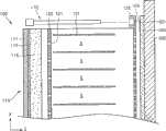
沉积单元730包括至少一个沉积室。根据图1的实施例,沉积单元730可以包括第一室731和设置在第一室731中的多个薄膜沉积组件100、200、300、400。根据图1的实施例,包括第一薄膜沉积组件100、第二薄膜沉积组件200、第三薄膜沉积组件300、第四薄膜沉积组件400的四个薄膜沉积组件安装在第一室731中。然而,将要安装在第一室731中的薄膜沉积组件的数量可以根据沉积材料和沉积条件而变化。当执行沉积时,第一室731具有在其中保持的适当程度的真空。The deposition unit 730 includes at least one deposition chamber. According to the embodiment of FIG. 1 , the deposition unit 730 may include a
此外,根据本发明的另一实施例,如图2中所示,沉积单元730包括彼此连接的第一室731和第二室732,第一薄膜沉积组件100和第二薄膜沉积组件200可以设置在第一室731中,第三薄膜沉积组件300和第四薄膜沉积组件400可以设置在第二室732中。当然,室的数量不限于此且可以增加。In addition, according to another embodiment of the present invention, as shown in FIG. 2 , the deposition unit 730 includes a
根据图1的实施例,第一循环单元610将设置有基底500的静电吸盘600至少移动到沉积单元730,设置有基底500的静电吸盘600可以顺序地移动到装载单元710、沉积单元730、卸载单元720。第二循环单元620使在卸载单元720中与基底500分开的静电吸盘600返回到装载单元710。According to the embodiment of FIG. 1 , the first circulation unit 610 moves the
第一循环单元610设置为在穿过沉积单元730时穿过第一室731,第二循环单元620允许静电吸盘600被传送到装载单元710。The first circulation unit 610 is provided to pass through the
图4是图1的薄膜沉积设备的第一循环单元610的剖视图。FIG. 4 is a cross-sectional view of the first circulation unit 610 of the thin film deposition apparatus of FIG. 1 .
第一循环单元610包括第一载具611,第一载具611允许设置有基底500的静电吸盘600移动。The first circulation unit 610 includes a first carrier 611 which allows the
第一载具611包括第一支撑件613、第二支撑件614、移动杆615、第一驱动单元616。The first carrier 611 includes a first support 613 , a second support 614 , a moving
第一支撑件613和第二支撑件614安装成穿过沉积单元730的室,例如,在图1的实施例中,第一支撑件613和第二支撑件614安装成穿过第一室731,在图2的实施例中,第一支撑件613和第二支撑件614安装成穿过第一室731和第二室732。The first support 613 and the second support 614 are installed to pass through the chamber of the deposition unit 730, for example, in the embodiment of FIG. 1, the first support 613 and the second support 614 are installed to pass through the
第一支撑件613竖直地设置在第一室731中,第二支撑件614水平地设置在第一室731中并在第一支撑件613下方。如图4中所示,第一支撑件613和第二支撑件614设置为彼此垂直以形成弯曲的结构。然而,本发明的各方面不限于此。第一支撑件613可以设置在第二支撑件614上方,第二支撑件614可以设置在第一支撑件613下方。The first supporter 613 is vertically disposed in the
移动杆615可沿第一支撑件613移动。移动杆615的至少一端由第一支撑件613支撑,移动杆615的另一端形成为被静电吸盘600的边缘支撑。静电吸盘600可以固定地支撑在移动杆615上,并可以因移动杆615而沿第一支撑件613移动。移动杆615的支撑静电吸盘600的一部分可以朝向薄膜沉积组件100弯曲,并可以允许基底500靠近薄膜沉积组件100。The moving
第一驱动单元616设置在移动杆615和第一支撑件613之间。第一驱动单元616可以包括辊617,辊617可沿第一支撑件613滚动。第一驱动单元616允许移动杆615沿第一支撑件613移动,并可以提供驱动力或可以将由另外的驱动源产生的驱动力传输到移动杆615。第一驱动单元616可以为允许移动杆615和辊617移动的任意的驱动装置。The
图5是图1的薄膜沉积设备的第二循环单元620的剖视图。FIG. 5 is a cross-sectional view of the
第二循环单元620包括第二载具621,第二载具621允许与基底500分开的静电吸盘600移动。The
第二载具621包括第三支撑件623、移动杆615、第一驱动单元616。The
第三支撑件623延伸的长度与第一载具611的第一支撑件613的延伸的长度相同。第三支撑件623支撑设置有第一驱动单元616的移动杆615,与基底500分开的静电吸盘600安装在移动杆615上。移动杆615和第一驱动单元616的结构如上所述。The extended length of the third supporting
下面,将描述设置在第一室731中的薄膜沉积组件100。图6是根据本发明实施例的薄膜沉积组件100的透视图,图7是根据本发明实施例的图6的薄膜沉积组件100的示意性剖面侧视图,图8是根据本发明实施例的薄膜沉积组件100的示意性平面图。Next, the thin
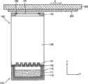
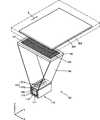
参照图6至图8,薄膜沉积组件100包括沉积源110、沉积源喷嘴单元120、图案化缝隙片150。Referring to FIGS. 6 to 8 , the thin
具体地讲,为了按期望的图案将从沉积源110发射并排放通过沉积源喷嘴单元120和图案化缝隙片150的沉积材料115沉积到基底500上,与使用精细金属掩模(FMM)的沉积方法中相同,第一室731应保持在高真空状态。另外,图案化缝隙片150的温度应足够地低于沉积源110的温度。就此,图案化缝隙片150的温度可以为大约100℃或更低。图案化缝隙片150的温度应足够低,从而减小图案化缝隙片150的热膨胀。Specifically, in order to deposit the
构成将沉积有沉积材料115的沉积目标(target)的基底500设置在第一室731中。基底500可以为用于平板显示器的基底。用于制造多个平板显示器的诸如母玻璃的大基底可以用作基底500。也可以采用其他的基底。The
可以在基底500或薄膜沉积组件100彼此相对地移动的同时执行沉积。Deposition may be performed while the
具体地讲,在传统的FMM沉积方法中,FMM的尺寸需要等于基底的尺寸。因此,FMM的尺寸需要随基底变得更大而增加。然而,既不易于制造大FMM,也不易于将FMM延展为与图案精确对准。Specifically, in conventional FMM deposition methods, the size of the FMM needs to be equal to the size of the substrate. Therefore, the size of the FMM needs to increase as the substrate becomes larger. However, it is neither easy to fabricate large FMMs nor to stretch the FMMs into precise alignment with the pattern.
为了克服这样的问题,在根据本发明实施例的薄膜沉积组件100中,可以在薄膜沉积组件100或基底500彼此相对地移动的同时执行沉积。换句话说,可以在设置为面对薄膜沉积组件100的基底500沿Y轴方向移动的同时连续地执行沉积。换句话说,在基底500沿图6中的箭头A的方向移动的同时以扫描的方式来执行沉积。In order to overcome such problems, in the thin
在薄膜沉积组件100中,图案化缝隙片150可以明显地小于在传统的沉积方法中使用的FMM。换句话说,在薄膜沉积组件100中,在基底500沿Y轴方向移动的同时连续地,即,以扫描的方式执行沉积。因此,图案化缝隙片150的沿X轴方向和Y轴方向的长度可以明显小于基底500的沿X轴方向和Y轴方向的长度。如上所述,因为图案化缝隙片150可以形成为显著地小于在传统的沉积方法中使用的FMM,所以制造在本发明的各方面中使用的图案化缝隙片150相对容易。换句话说,与使用更大的FMM的传统的沉积方法相比,在包括蚀刻和其他的后续工艺(诸如精确延展、焊接、移动、清洁工艺)的所有的工艺中,使用小于在传统的沉积方法中使用的FMM的图案化缝隙片150更加方便。这样更有利于相对大的显示设备。In the thin
含有并加热沉积材料115的沉积源110设置在第一室731的与设置有基底500的一侧相对的一侧。在包含在沉积源110中的沉积材料115蒸发的同时,沉积材料115沉积在基底500上。A
具体地讲,沉积源110包括:坩埚112,填充有沉积材料115;冷却阻挡件111,包括加热器(未示出),加热器加热坩埚112以使包含在坩埚112中的沉积材料115朝向坩埚112的侧部蒸发,具体地讲,朝向沉积源喷嘴单元120蒸发。冷却阻挡件111防止来自坩埚112的热辐射到外部,即,辐射到第一室731中。Specifically, the
沉积源喷嘴单元120设置在沉积源110的侧部处,具体地讲,设置在沉积源110的面对基底500的侧部处。沉积源喷嘴单元120包括沿Y轴方向(即,基底500的扫描方向)按相等的间距布置的多个沉积源喷嘴121。在沉积源110中蒸发的沉积材料115穿过沉积源喷嘴单元120朝向基底500。如上所述,当沉积源喷嘴单元120包括沿Y轴方向(即,基底500的扫描方向)布置的多个沉积源喷嘴121时,由排放通过图案化缝隙片150的图案化缝隙151的沉积材料115形成的图案的尺寸受每个沉积源喷嘴121的尺寸的影响(这是因为沿X轴方向仅有一行沉积源喷嘴),因此,在基底500上可以不形成阴影区域。此外,因为多个沉积源喷嘴121沿基底500的扫描方向布置,所以即使当沉积源喷嘴121之间存在流量差异时,也可以补偿该差异并可以恒定地保持沉积均匀性。The deposition
图案化缝隙片150和结合有图案化缝隙片150的框架155设置在沉积源110和基底500之间。框架155可以按与窗口框架(window frame)类似的格子形状(1attice shape)形成。图案化缝隙片150结合在框架155内。图案化缝隙片150包括沿X轴方向布置的多个图案化缝隙151。在沉积源110中蒸发的沉积材料115穿过沉积源喷嘴单元120和图案化缝隙片150朝向基底500。可以通过作为在制造FMM(具体地讲,条纹式FMM)的传统方法中使用的方法相同的方法的蚀刻来制造图案化缝隙片150。就此,图案化缝隙151的总数可以大于沉积源喷嘴121的总数。The
另外,沉积源110和结合到沉积源110的沉积源喷嘴单元120可以设置为与图案化缝隙片150分开预定的距离。可选择地,沉积源110和结合到沉积源110的沉积源喷嘴单元120可以由第一连接构件135连接到图案化缝隙片150。即,沉积源110、沉积源喷嘴单元120、图案化缝隙片150可以通过经第一连接构件135连接彼此而整体化地形成为一体。第一连接构件135引导排放通过沉积源喷嘴121的沉积材料151基本上为直线地运动通过薄膜沉积组件100,且不沿X轴方向流动。在图6中,第一连接构件135形成在沉积源110、沉积源喷嘴单元120、图案化缝隙片150的左侧和右侧上,以引导沉积材料115不沿X轴方向流动;然而,本发明的各方面不限于此。即,第一连接构件135可以形成为密封的盒子,以在X轴方向和Y轴方向上引导沉积材料115的流动。In addition, the
如上所述,薄膜沉积组件100在相对于基底500移动的同时执行沉积。为了相对于基底500移动薄膜沉积组件100,图案化缝隙片150与基底500分开预定的距离。As described above, the thin
具体地讲,在利用FMM的传统沉积方法中,为了防止在基底上形成阴影区域,在FMM与基底紧密接触的情况下用FMM执行沉积。然而,当使用与基底紧密接触的FMM时,这样的接触会引起缺陷。另外,在传统沉积方法中,由于掩模不能相对于基底移动,所以掩模的尺寸需要与基底的尺寸相同。因此,掩模的尺寸需要随着显示设备变得更大而增大。然而,不容易制造这样的大的掩模。In particular, in the conventional deposition method using the FMM, in order to prevent a shadow region from being formed on the substrate, the deposition is performed with the FMM while the FMM is in close contact with the substrate. However, when using FMMs that are in intimate contact with the substrate, such contact can cause defects. In addition, in the conventional deposition method, since the mask cannot be moved relative to the substrate, the size of the mask needs to be the same as that of the substrate. Therefore, the size of the mask needs to increase as the display device becomes larger. However, it is not easy to manufacture such a large mask.
为了克服这样的问题,在薄膜沉积组件100中,图案化缝隙片150被设置为与基底500分开预定的距离。In order to overcome such a problem, in the thin
如上所述,掩模被形成为小于基底,并且在掩模相对于基底移动的同时执行沉积。因此,可以容易地制造掩模。另外,可以防止在传统沉积方法中出现的因基底和FMM之间的接触而引起的缺陷。另外,由于在沉积工艺期间不需要将FMM设置为与基底紧密接触,所以可以缩短制造时间。As described above, the mask is formed smaller than the substrate, and deposition is performed while the mask is moved relative to the substrate. Therefore, a mask can be easily manufactured. In addition, defects caused by contact between the substrate and the FMM, which occur in conventional deposition methods, can be prevented. In addition, since the FMM does not need to be placed in close contact with the substrate during the deposition process, manufacturing time can be shortened.
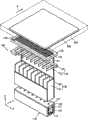
图9是根据本发明另一实施例的薄膜沉积组件100的透视图。参照图9,薄膜沉积组件100包括沉积源110、沉积源喷嘴单元120、图案化缝隙片150。具体地讲,沉积源110包括填充有沉积材料115的坩埚112和包括加热器(未示出)的冷却阻挡件111,加热器加热坩埚112以使沉积材料115蒸发,从而使蒸发的沉积材料115向沉积源喷嘴单元120运动。冷却阻挡件111围绕坩埚112。具有平面形状的沉积源喷嘴单元120设置在沉积源110的侧部处。沉积源喷嘴单元120包括沿Y轴方向布置的多个沉积源喷嘴121。此外,图案化缝隙片150和框架155设置在沉积源110和基底500之间。图案化缝隙片150包括沿X轴方向布置的多个图案化缝隙151。另外,沉积源110和沉积源喷嘴单元120可以通过(在图11中示出的)第二连接构件133连接到图案化缝隙片150。FIG. 9 is a perspective view of a thin
与参照图6描述的薄膜沉积组件100不同,形成在沉积源喷嘴单元120上的多个沉积源喷嘴121按预定的角度倾斜。具体地讲,沉积源喷嘴121可以包括布置在相应的行中的沉积源喷嘴121a和121b。沉积源喷嘴121a和121b可以布置在相应的行中以按Z字形图案交替。沉积源喷嘴121a和121b可以在XZ平面上倾斜预定的角度。Unlike the thin
沉积源喷嘴121a和121b被布置为彼此倾斜预定角度。第一行中的沉积源喷嘴121a和第二行中的沉积源喷嘴121b可以倾斜以彼此面对。即,沉积源喷嘴单元120的左部中的第一行的沉积源喷嘴121a可以倾斜以面对图案化缝隙片150的右侧部,沉积源喷嘴单元120的右部中的第二行的沉积源喷嘴121b可以倾斜以面对图案化缝隙片150的左侧部。The
由于根据当前实施例的薄膜沉积组件100的结构,所以可以调节沉积材料115的沉积以减小基底500的中心和端部之间的厚度变化,并且改善沉积膜的厚度均匀性。另外,还可以改善沉积材料115的利用效率。Due to the structure of the thin
图10是根据本发明另一实施例的薄膜沉积设备的透视图。参照图10,薄膜沉积设备包括多个薄膜沉积组件,每个薄膜沉积组件具有图6至图8中示出的薄膜沉积组件100的结构。换句话说,图10中示出的薄膜沉积设备可以包括同时排放用于形成红(R)发射层、绿(G)发射层、蓝(B)发射层的沉积材料的多沉积源。FIG. 10 is a perspective view of a thin film deposition apparatus according to another embodiment of the present invention. Referring to FIG. 10 , the thin film deposition apparatus includes a plurality of thin film deposition assemblies each having the structure of the thin
具体地讲,薄膜沉积设备包括第一薄膜沉积组件100、第二薄膜沉积组件200、第三薄膜沉积组件300。第一薄膜沉积组件100、第二薄膜沉积组件200、第三薄膜沉积组件300中的每个薄膜沉积组件的结构与参照图6至图8描述的薄膜沉积组件100的结构相同,因此,这里将不提供它们的详细描述。Specifically, the thin film deposition equipment includes a first thin
第一薄膜沉积组件100、第二薄膜沉积组件200、第三薄膜沉积组件300的沉积源110可以分别包含不同的沉积材料。第一薄膜沉积组件100可以包含用于形成R发射层的沉积材料,第二薄膜沉积组件200可以包含用于形成G发射层的沉积材料,第三薄膜沉积组件300可以包含用于形成B发射层的沉积材料。The deposition sources 110 of the first thin
换句话说,在制造有机发光显示设备的传统方法中,使用单独的室和掩模以形成每种色彩发射层。然而,当使用根据本发明实施例的薄膜沉积设备时,可以以单个的多沉积源来同时形成R发射层、G发射层、B发射层。因此,制造有机发光显示设备所用的时间显著地减少。另外,可以利用数量减少的室来制造有机发光显示设备,从而还显著地减少设备成本。In other words, in a conventional method of manufacturing an organic light emitting display device, separate chambers and masks are used to form each color emission layer. However, when using the thin film deposition apparatus according to the embodiment of the present invention, the R emission layer, the G emission layer, and the B emission layer can be simultaneously formed with a single multi-deposition source. Therefore, the time taken to manufacture an organic light emitting display device is significantly reduced. In addition, an organic light emitting display device can be manufactured with a reduced number of chambers, thereby also significantly reducing device cost.
虽然没有示出,但是第一薄膜沉积组件100的图案化缝隙片、第二薄膜沉积组件200的图案化缝隙片、第三薄膜沉积组件300的图案化缝隙片可以布置为相对于彼此偏移恒定的距离,从而使与图案化缝隙片对应的沉积区域在基底500上不叠置。换句话说,当第一薄膜沉积组件100、第二薄膜沉积组件200、第三薄膜沉积组件300分别用于沉积R发射层、G发射层、B发射层时,第一薄膜沉积组件100的图案化缝隙、第二薄膜沉积组件200的图案化缝隙、第三薄膜沉积组件300的图案化缝隙布置为彼此不对准,以在基底500的不同的区域中形成R发射层、G发射层、B发射层。Although not shown, the patterned slit sheet of the first thin
此外,用于形成R发射层、G发射层、B发射层的沉积材料可以具有不同的沉积温度。因此,可以将第一薄膜沉积组件100、第二薄膜沉积组件200、第三薄膜沉积组件300的沉积源的温度设置为不同。In addition, deposition materials used to form the R emission layer, the G emission layer, and the B emission layer may have different deposition temperatures. Therefore, the temperatures of the deposition sources of the first thin
虽然根据本发明实施例的图10中示出的薄膜沉积设备包括三个薄膜沉积组件,但是本发明不限于此。换句话说,根据本发明另一实施例的薄膜沉积设备可以包括多个薄膜沉积组件,每个薄膜沉积组件包含不同的沉积材料。例如,根据本发明另一实施例的薄膜沉积设备可以包括分别包含用于R发射层、G发射层、B发射层、R发射层的辅助层(R’)、G发射层的辅助层(G’)的材料的五个薄膜沉积组件。Although the thin film deposition apparatus shown in FIG. 10 according to an embodiment of the present invention includes three thin film deposition assemblies, the present invention is not limited thereto. In other words, a thin film deposition apparatus according to another embodiment of the present invention may include a plurality of thin film deposition components, each of which contains a different deposition material. For example, a thin film deposition apparatus according to another embodiment of the present invention may include an auxiliary layer (G') including an auxiliary layer (R') for an R emission layer, a G emission layer, a B emission layer, an R emission layer, and a G emission layer, respectively. ') of five thin-film deposition components of the material.
如上所述,可以利用多个薄膜沉积组件同时形成多个薄层。因此,改善了生产率和沉积效率。此外,简化了整个制造工艺,降低了制造成本。As described above, multiple thin layers can be formed simultaneously using multiple thin film deposition assemblies. Therefore, productivity and deposition efficiency are improved. In addition, the entire manufacturing process is simplified and the manufacturing cost is reduced.
图11是根据本发明另一实施例的薄膜沉积组件100的透视图,图12是根据本发明实施例的图11的薄膜沉积组件100的示意性剖面侧视图,图13是根据本发明实施例的图11的薄膜沉积组件100的示意性平面图。11 is a perspective view of a thin
参照图11至图13,薄膜沉积组件100包括沉积源110、沉积源喷嘴单元120、障碍墙组件130、图案化缝隙片150。Referring to FIGS. 11 to 13 , the thin
虽然为了方便说明而没有在图11至图13中示出室,但是薄膜沉积组件100的所有组件可以设置在室内,在室中保持适当程度的真空。室具有在其中保持的适当的真空,以允许沉积材料基本上为直线地运动通过薄膜沉积组件100。Although the chamber is not shown in FIGS. 11 to 13 for convenience of illustration, all components of the thin
通过使用静电吸盘600将构成将沉积有沉积材料115的目标的基底500传送到室中。基底500可以为用于平板显示器的基底。诸如用于制造多个平板显示器的母玻璃的大基底可以用作基底500。The
可以在基底500或薄膜沉积组件100彼此相对地移动的同时执行沉积。基底500可以沿方向A相对于薄膜沉积组件100移动。Deposition may be performed while the
与上述的图6的实施例相同,在根据本发明当前实施例的薄膜沉积组件100中,图案化缝隙片150可以显著地小于在传统的沉积方法中使用的FMM。换句话说,在薄膜沉积组件100中,在基底500沿Y轴方向移动的同时连续地,即,以扫描的方式执行沉积。因此,如果图案化缝隙片150的沿X轴方向的宽度与基底500的沿X轴方向的宽度基本相同,则图案化缝隙片150的沿Y轴方向的长度可以显著地小于基底500的沿Y轴方向的长度。当然,即使当图案化缝隙片150的沿X轴方向的宽度小于基底500的沿X轴方向的宽度时,因基底500和薄膜沉积组件100的相对运动而可以充分地在基底500的整个表面上以扫描的方式来执行沉积。Like the embodiment of FIG. 6 described above, in the thin
如上所述,因为图案化缝隙片150可以形成为明显小于在传统的沉积方法中使用的FMM,所以制造在本发明的一方面中使用的图案化缝隙片150是相对容易的。换句话说,与使用更大的FMM的传统的沉积方法相比,在包括蚀刻和后续的其他工艺(诸如精确延展、焊接、移动、清洁工艺)的所有的工艺中,使用小于在传统的沉积方法中使用的FMM的图案化缝隙片150更加方便。这样更有利于相对大的显示设备。As described above, since the
包含并加热沉积材料115的沉积源110设置在室的与设置有基底500的一侧相对的一侧中。A
沉积源110包括:坩埚112,填充有沉积材料115;冷却阻挡件111,围绕坩埚112。冷却阻挡件111防止来自坩埚112的热辐射到外部,即,防止来自坩埚112的热辐射到室中。冷却阻挡件111可以包括加热坩埚112的加热器(未示出)。The
沉积源喷嘴单元120设置在沉积源110的侧部处,具体地讲,在沉积源110的面对基底500的侧部处。沉积源喷嘴单元120包括沿X轴方向布置的多个沉积源喷嘴121。在沉积源110中蒸发的沉积材料115穿过沉积源喷嘴单元120的多个沉积源喷嘴121朝向基底500。The deposition
障碍墙组件130设置在沉积源喷嘴单元120的侧部处。障碍墙组件130包括多个障碍墙131和构成障碍墙131的外壁的障碍墙框架132。多个障碍墙131可以沿X轴方向按相等的间距布置为彼此平行。另外,每个障碍墙131可以形成为沿图11中的YZ平面延伸,即,可以形成为垂直于X轴方向延伸。如上所述地布置的多个障碍墙131将沉积源喷嘴单元120和图案化缝隙片150之间的空间划分为多个子沉积空间S(在图13中示出)。在薄膜沉积组件100中,障碍墙131将沉积空间分为分别对应于沉积材料115排放所通过的沉积源喷嘴121的子沉积空间S,如图13中所示。The
障碍墙131可以分别设置在相邻的沉积源喷嘴121之间。换句话说,每个沉积源喷嘴121可以设置在两个相邻的障碍墙131之间。沉积源喷嘴121可以分别位于两个相邻的障碍墙131之间的中点处。然而,本发明的各方面不限于此,且可以以其他方式设置沉积源喷嘴121。多个沉积源喷嘴121可以设置在两个相邻的障碍墙131之间。即使在这样的情况下,沉积源喷嘴121也可以分别位于两个相邻的障碍墙131之间的中点处。
如上所述,因为障碍墙131将沉积源喷嘴单元120和图案化缝隙片150之间的空间划分成多个子沉积空间S,所以排放通过每个沉积源喷嘴121的沉积材料115没有与排放通过其他沉积源喷嘴121的沉积材料115混合,并穿过图案化缝隙151,从而沉积在基底500上。换句话说,障碍墙131引导排放通过沉积源喷嘴121的沉积材料115沿基本上为直线地运动通过薄膜沉积组件100,且不沿X轴方向流动。As described above, since the
如上所述,通过安装障碍墙131,沉积材料115被迫使沿基本上为直线地运动通过薄膜沉积组件100,从而与没有安装障碍墙的情况相比,可在基底500上形成更小的阴影区域。因此,薄膜沉积组件100和基底500可以彼此分开预定的距离。这将在下面进行详细描述。As mentioned above, by installing the
形成障碍墙131的上侧和下侧的障碍墙框架132保持障碍墙131的位置,并引导排放通过沉积源喷嘴121的沉积材料115沿基本上为直线地运动通过薄膜沉积组件100,且不沿Y轴方向流动。The barrier wall frame 132 forming the upper and lower sides of the
沉积源喷嘴单元120和障碍墙组件130可以彼此分开预定的距离。因此,可以防止从沉积源110散发的热传导到障碍墙组件130。然而,本发明的各方面不限于此。换句话说,当将合适的绝缘单元设置在沉积源喷嘴单元120和障碍墙组件130之间时,可以将沉积源喷嘴单元120和障碍墙组件130彼此组合并可以彼此接触。The deposition
另外,障碍墙组件130可以被构造为可从薄膜沉积组件100拆下。为了克服这样的问题,在薄膜沉积组件100中,通过使用障碍墙组件130围绕沉积空间,使得剩余的未沉积的沉积材料115大部分沉积在障碍墙组件130内。因此,因为障碍墙组件130被构造为可从薄膜沉积组件100拆下,所以当在长时间的沉积工艺之后大量沉积材料115处于障碍墙组件130中时,可以将障碍墙组件130从薄膜沉积组件100拆下,然后置于单独的沉积材料回收设备中以回收沉积材料115。因根据本实施例的薄膜沉积组件100的结构,提高了沉积材料115的再利用率,从而改善了沉积效率,并因此降低了制造成本。In addition, the
图案化缝隙片150和结合有图案化缝隙片150的框架155设置在沉积源110和基底500之间。框架155可以以与窗口框架类似的格子形状形成。图案化缝隙片150结合在框架155内。图案化缝隙片150包括沿X轴方向布置的多个图案化缝隙151。图案化缝隙片150沿Y轴方向延伸。在沉积源110中蒸发并穿过沉积源喷嘴121的沉积材料115穿过图案化缝隙151朝向基底500。The
图案化缝隙片150由金属片形成,并以延展的状态结合在框架155上。在通过蚀刻制造的图案化缝隙片150中,图案化缝隙151形成为条纹式缝隙。The
在薄膜沉积组件100中,图案化缝隙151的总数可以大于沉积源喷嘴121的总数。另外,可以有数量比沉积源喷嘴121的数量更大的图案化缝隙151设置在两个相邻的障碍墙131之间。图案化缝隙151的数量可以对应于将要形成在基底500上的沉积图案的数量。In the thin
另外,障碍墙组件130和图案化缝隙片150可以形成为彼此分开预定的距离。可选择地,障碍墙组件130和图案化缝隙片150可以通过单独的第二连接构件133连接。障碍墙组件130的温度可以因高温的沉积源110而增加到100℃或更高。因此,为了防止障碍墙组件130的热传导到图案化缝隙片150,将障碍墙组件130和图案化缝隙片150彼此分开预定的距离。In addition, the
如上所述,薄膜沉积组件100在相对于基底500移动的同时执行沉积。为了相对于基底500移动薄膜沉积组件100,将图案化缝隙片150与基底500分开预定的距离。另外,为了防止当图案化缝隙片150和基底500彼此分开时在基底500上形成相对大的阴影区域,将障碍墙131布置在沉积源喷嘴单元120和图案化缝隙片150之间,以迫使沉积材料115沿直线方向运动。因此,显著地减小了形成在基底500上的阴影区域的尺寸。As described above, the thin
具体地讲,在利用FMM的传统的沉积方法中,利用与基底紧密接触的FMM来执行沉积,以防止在基底上形成阴影区域。然而,当使用与基底紧密接触的FMM时,出现诸如因基底和FMM之间的接触而划伤已经形成在基底上方的图案的缺陷。另外,在传统的沉积方法中,因为掩模不能相对于基底移动,所以掩模的尺寸需要与基底的尺寸相同。因此,掩模的尺寸需要随着显示设备变得更大而增大。然而,不容易制造这样的大的掩模。Specifically, in the conventional deposition method using the FMM, deposition is performed using the FMM in close contact with the substrate to prevent shadow regions from being formed on the substrate. However, when an FMM in close contact with a substrate is used, defects such as scratching of a pattern already formed over the substrate due to contact between the substrate and the FMM occur. In addition, in the conventional deposition method, since the mask cannot move relative to the substrate, the size of the mask needs to be the same as that of the substrate. Therefore, the size of the mask needs to increase as the display device becomes larger. However, it is not easy to manufacture such a large mask.
为了克服这样的问题,在根据本发明一方面的薄膜沉积组件100中,图案化缝隙片150被设置为与基底500分开预定的距离。可以通过安装障碍墙131以减小形成在基底500上的阴影区域的尺寸,而有助于将图案化缝隙片150与基底500分开预定的距离。In order to overcome such problems, in the thin
当根据本发明的一方面将图案化缝隙片形成为小于基底,然后相对于基底移动图案化缝隙片时,不需要制造与使用FMM的传统的沉积方法中相同的大掩模。另外,因为基底和图案化缝隙片彼此分开预定的距离,所以可以防止因基底和图案化缝隙片之间的接触导致的缺陷。另外,由于在沉积工艺期间不需要使用与基底紧密接触的图案化缝隙片,所以可以改善制造速度。When forming the patterned slit sheet smaller than the substrate and then moving the patterned slit sheet relative to the substrate according to an aspect of the present invention, there is no need to manufacture the same large mask as in the conventional deposition method using FMM. In addition, since the substrate and the patterned slit sheet are separated from each other by a predetermined distance, defects due to contact between the substrate and the patterned slit sheet can be prevented. In addition, since there is no need to use a patterned slit sheet in close contact with the substrate during the deposition process, manufacturing speed can be improved.
在薄膜沉积组件100中,如图14A和图14B中所示,沉积源110可以容纳在连接到第一室731的源室113中,在第一室731中执行沉积。In the thin
换言之,单独的源室113连接到将要执行沉积的第一室731,源室113和第一室731之间的空间由高真空阀118打开或关闭。In other words, the
为了在完成沉积工艺之后在沉积源110中再次填充沉积材料,应当将第一室731保持在大气压下。然而,当将第一室731保持在大气压下以再次填充沉积源110,然后将第一室731保持在真空状态以执行新的沉积工艺时,该过程耗时长且生产时间增加。In order to refill the deposition material in the
对此,在本发明的实施例中,支撑沉积源110的台114设置在源室113中,并将台114连接到伸缩管(bellows)116。随着驱动伸缩管116而驱动台114。因此,沉积源110可以在源室113和第一室731之间移动。For this, in an embodiment of the present invention, a
开闭器117设置在沉积源110的周围,当沉积源110上升到第一室731中时,开闭器117阻塞到源室113的连接开口,以防止源室113受到沉积材料的污染,如图14A所示。在完成沉积工艺之后,沉积源110在开闭器117打开时下降到源室113中,并且通过高真空阀118将源室113相对于第一室731以气密状态关闭,如图14B所示。在这种状态下,源室113的状态变成处于大气压下,设置在源室113中的单独的门(未示出)打开,从而可以从源室113取出沉积源110,以在沉积源110中再次填充沉积材料。根据该结构,可以容易地将沉积材料填充在沉积源110中,而无需对第一室731进行排气。The
此外,薄膜沉积组件100可以安装在第二支撑件614上,如图4所示。关于这点,第二驱动单元618设置在第二支撑件614上,并且第二驱动单元618连接到薄膜沉积组件100的框架155并精细地调整薄膜沉积组件100的位置,使得基底500和薄膜沉积组件100可以相互对准。可以在执行沉积工艺的同时实时执行对准的调整。In addition, the thin
薄膜沉积组件100还可以包括相机组件170,用来将基底500和薄膜沉积组件100相互对准,如图11和图13所示。相机组件170用来将形成在框架155上的第一标记159与形成在基底500上的第二标记501实时地彼此对准。The thin
相机组件170可以获得在执行沉积工艺的真空室内宽的观察区域,如图10所示。换言之,如图15所示,相机172设置在圆柱形罩171中,包括透镜的光学系统173设置在相机172和罩171的开口176之间。形成有加热图案175的保护窗174设置在光学系统173和开口176之间。在执行沉积工艺的同时,通过利用加热图案175,有机材料不沉积在保护窗174的表面上。因此,即使在执行沉积工艺时,相机172也可以通过保护窗174确定真空室内的对准。The
图16是根据本发明另一实施例的薄膜沉积组件100的示意性透视图。FIG. 16 is a schematic perspective view of a thin
参照图16,薄膜沉积组件100包括沉积源110、沉积源喷嘴单元120、第一障碍墙组件130、第二障碍墙组件140和图案化缝隙片150。Referring to FIG. 16 , the thin
虽然为了便于解释而没有在图16中示出室,但是薄膜沉积组件100的所有组件都可以设置在保持着适当真空度的室内。室内保持有适当的真空,以使沉积材料能够穿过薄膜沉积组件100基本上沿着直线移动。Although the chamber is not shown in FIG. 16 for convenience of explanation, all components of the thin
构成将要沉积有沉积材料115的目标的基底500设置在室中。包含并加热沉积材料115的沉积源110设置在室的与设置有基底500的一侧相对的一侧。A
沉积源110和图案化缝隙片150的详细结构与图11中的沉积源110和图案化缝隙片150的详细结构相同,因此,在此将不提供对它们的详细描述。第一障碍墙组件130与参照图11的实施例描述的障碍墙组件130相同,因此在此将不提供对它的详细描述。The detailed structures of the
第二障碍墙组件140设置在第一障碍墙组件130的一例。第二障碍墙组件140包括多个第二障碍墙141和构成第二障碍墙141的外壁的第二障碍墙框架142。The second barrier wall unit 140 is provided on an example of the first
多个第二障碍墙141可以沿着X轴方向以相等的间距彼此平行地布置。此外,每个第二障碍墙141可以形成为沿着图16中的YZ面延伸,即,垂直于X轴方向延伸。The plurality of second barrier walls 141 may be arranged parallel to each other at equal intervals along the X-axis direction. In addition, each second barrier wall 141 may be formed to extend along the YZ plane in FIG. 16 , that is, to extend perpendicular to the X-axis direction.
按上面的描述布置的多个第一障碍墙131和第二障碍墙141划分沉积源喷嘴单元120和图案化缝隙片150之间的空间。在图16中示出的薄膜沉积组件100中,第一障碍墙131和第二障碍墙141将沉积空间分成分别对应于沉积源喷嘴121的子沉积空间,其中,通过沉积源喷嘴121排出沉积材料115。The plurality of
可以将第二障碍墙141设置成分别对应于第一障碍墙131。换言之,第二障碍墙141可以分别设置成平行于第一障碍墙131并与第一障碍墙131位于同一平面上。每对对应的第一障碍墙131和第二障碍墙141可以位于同一平面上。虽然第一障碍墙131和第二障碍墙141被示出为沿X轴方向具有相同的厚度,但是本发明的多个方面不限于此。换言之,需要与图案化缝隙片150精确对准的第二障碍墙141可以形成得相对薄,而不需要与图案化缝隙片150精确对准的第一障碍墙131可以形成得相对厚。这样更容易制造薄膜沉积组件100。The second barrier walls 141 may be disposed corresponding to the
如上所述的多个薄膜沉积组件100可以连续地布置在第一室731中,如图1所示。关于这点,第一至第四薄膜沉积组件100、200、300和400(见图1)可以沉积不同的沉积材料。关于这点,第一至第四薄膜沉积组件100、200、300和400的图案化缝隙的图案互不相同,从而可以同时执行包括沉积红色像素、绿色像素和蓝色像素的工艺的层形成工艺。A plurality of thin
图17是根据本发明实施例的利用薄膜沉积设备制造的有源矩阵(AM)有机发光显示设备的剖视图。17 is a cross-sectional view of an active matrix (AM) organic light emitting display device manufactured using a thin film deposition device according to an embodiment of the present invention.
参照图17,AM有机发光显示设备设置在基底30上。基底30可以由透明材料(例如,玻璃)形成,也可以由塑料或金属形成。诸如缓冲层的绝缘层31形成在基底30上。Referring to FIG. 17 , an AM organic light emitting display device is disposed on a
薄膜晶体管(TFT)40、电容器50、有机发光装置60形成在绝缘层31上,如图17所示。A thin film transistor (TFT) 40, a
半导体有源层41以预定的图案形成在绝缘层31的上表面上。栅极绝缘层32形成为覆盖半导体有源层41。半导体有源层41可以包含p型半导体材料或n型半导体材料。The semiconductor
TFT 40的栅电极42对应于半导体有源层41形成在栅极绝缘层32的上表面上。层间绝缘层33形成为覆盖栅电极42。在形成层间绝缘层33之后,通过例如执行干蚀刻来蚀刻栅极绝缘层32和层间绝缘层33,以形成暴露半导体有源层41的部分的接触孔。The
接下来,源/漏电极43形成在层间绝缘层33上,以通过接触孔接触半导体有源层41。钝化层34形成为覆盖源/漏电极43,并被蚀刻为暴露源/漏电极43的一部分。单独的绝缘层(未示出)还可以形成在钝化层34上,以使钝化层34平坦化。Next, source/
此外,有机发光装置60随着电流流动发射红光、绿光或蓝光而显示预定的图像信息。有机发光装置60包括形成在钝化层34上的第一电极61。第一电极61电连接到TFT 40的漏电极43。In addition, the organic
像素限定层35形成为覆盖第一电极61。在开口64形成在像素限定层35中之后,有机发射层63形成在由开口64限定的区域中。第二电极62形成在有机发射层63上。The
限定单个像素的像素限定层35由有机材料形成。像素限定层35还使基底30的形成有第一电极61的区域的表面(具体地讲,钝化层34的表面)平坦化。The
第一电极61和第二电极62彼此绝缘,并且分别将极性相反的电压施加到有机发射层63,以在有机发射层63中引起发光。The
有机发射层63可以由低分子量有机材料或聚合物有机材料形成。当使用低分子量有机材料时,有机发射层63可以具有包括从由空穴注入层(HIL)、空穴传输层(HTL)、发射层(EML)、电子传输层(ETL)、电子注入层(EIL)等组成的组中选择的至少一层的单层结构或多层结构。可用的有机材料的示例可以包括铜酞菁(CuPc)、N,N′-二(萘-1-基)-N,N′-二苯基-联苯胺(NPB,N,N′-di(naphthalene-1-yl)-N,N′-diphenyl-benzidine)、三-8-羟基喹啉铝(Alq3)等。可以利用上面参照图1至图16描述的薄膜沉积设备之一通过真空沉积来沉积这种低分子量有机材料。The
首先,在像素限定层35中形成开口64之后,将基底30传送到室731中,如图1所示。通过第一至第四薄膜沉积组件100、200、300和400来沉积目标有机材料。First, after the
在形成有机发射层63之后,可以通过执行与用来形成第一电极61的沉积工艺相同的沉积工艺来形成第二电极62。After the
第一电极61用作阳极,第二电极62用作阴极。可选择地,第一电极61可以用作阴极,第二电极62可以用作阳极。第一电极61可以图案化为与单个的像素区域对应,第二电极62可以形成为覆盖所有的像素。The
第一电极61可以形成为透明电极或反射电极。这样的透明电极可以由至少一种选自于由氧化铟锡(ITO)、氧化铟锌(IZO)、氧化锌(ZnO)和氧化铟(In2O3)组成的组中的材料形成。这样的反射电极可以通过以下步骤形成:利用选自于由银(Ag)、镁(Mg)、铝(Al)、铂(Pt)、钯(Pd)、金(Au)、镍(Ni)、钕(Nd)、铱(Ir)、铬(Cr)和它们的混合物组成的组中的至少一种材料形成反射层;在反射层上利用由ITO、IZO、ZnO和In2O3组成的组中选择的至少一种材料形成一层。可以通过例如溅射形成一层,然后通过例如光刻将该层图案化来形成第一电极61。The
第二电极62也可以形成为透明电极或反射电极。当第二电极62形成为透明电极时,第二电极62用作阴极。为此,可以通过在有机发射层63的表面上沉积诸如锂(Li)、钙(Ca)、氟化锂/钙(LiF/Ca)、氟化锂/铝(LiF/Al)、铝(Al)、银(Ag)、镁(Mg)或它们的混合物的功函数低的金属或金属盐,并由ITO、IZO、ZnO、In2O3等在所述金属或金属盐上形成辅助电极层或汇流电极线,来形成这样的透明电极。当第二电极62形成为反射电极时,可以通过在有机发射层63的整个表面上沉积由Li、Ca、LiF/Ca、LiF/Al、Al、Ag、Mg和它们的混合物组成的组中选择的至少一种材料来形成反射层。可以使用与上述的用来形成有机发射层63的方法相同的沉积方法来形成第二电极62。The
上面描述的根据本发明实施例的薄膜沉积设备可以用来形成有机TFT的有机层或无机层,并且可以用来形成由各种材料形成的层。The thin film deposition apparatus according to the embodiments of the present invention described above may be used to form an organic layer or an inorganic layer of an organic TFT, and may be used to form layers formed of various materials.
如上所述,在根据本发明各方面的薄膜沉积设备和根据本发明各方面的利用该薄膜沉积设备来制造有机发光显示设备的方法中,可以容易地使用该薄膜沉积设备来大规模地制造大基底。此外,可以容易地制造薄膜沉积设备和有机发光显示设备,并且薄膜沉积设备和有机发光显示设备可以提高生产率和沉积效率,并可以使沉积材料能够再利用。As described above, in the thin film deposition apparatus according to aspects of the present invention and the method of manufacturing an organic light-emitting display device using the thin film deposition apparatus according to aspects of the present invention, it is possible to easily use the thin film deposition apparatus to manufacture large-scale base. In addition, the thin film deposition apparatus and the organic light emitting display apparatus can be easily manufactured, and the thin film deposition apparatus and the organic light emitting display apparatus can improve productivity and deposition efficiency, and can enable reuse of deposited materials.
虽然已经参照本发明各方面的示例性实施例具体地示出和描述了本发明的各方面,但是本领域的普通技术人员应该理解,在不脱离由权利要求限定的本发明的精神和范围的情况下,可以在此做出各种形式和细节上的改变。Although various aspects of the present invention have been specifically shown and described with reference to exemplary embodiments of various aspects of the present invention, those skilled in the art should understand that, without departing from the spirit and scope of the present invention defined by the claims, Various changes in form and detail may be made herein.
Claims (39)
Translated fromChineseApplications Claiming Priority (4)
| Application Number | Priority Date | Filing Date | Title |
|---|---|---|---|
| KR20090079765 | 2009-08-27 | ||
| KR10-2009-0079765 | 2009-08-27 | ||
| KR10-2010-0011480 | 2010-02-08 | ||
| KR1020100011480AKR101174877B1 (en) | 2009-08-27 | 2010-02-08 | Apparatus for thin layer deposition and method for manufacturing of organic light emitting display apparatus using the same |
Publications (2)
| Publication Number | Publication Date |
|---|---|
| CN102005541Atrue CN102005541A (en) | 2011-04-06 |
| CN102005541B CN102005541B (en) | 2013-08-14 |
Family
ID=43221846
Family Applications (1)
| Application Number | Title | Priority Date | Filing Date |
|---|---|---|---|
| CN2010102664066AActiveCN102005541B (en) | 2009-08-27 | 2010-08-27 | Thin film deposition apparatus and method of manufacturing organic light-emitting display apparatus using the same |
Country Status (4)
| Country | Link |
|---|---|
| US (2) | US9450140B2 (en) |
| EP (1) | EP2290118B1 (en) |
| JP (1) | JP5677785B2 (en) |
| CN (1) | CN102005541B (en) |
Cited By (20)
| Publication number | Priority date | Publication date | Assignee | Title |
|---|---|---|---|---|
| CN102433540A (en)* | 2011-08-30 | 2012-05-02 | 费绍栋 | Window type device for detecting surface parameters of material in direct contact way in vacuum environment |
| CN102867919A (en)* | 2011-07-04 | 2013-01-09 | 三星显示有限公司 | Organic layer deposition apparatus |
| CN102867924A (en)* | 2011-07-04 | 2013-01-09 | 三星显示有限公司 | Organic layer deposition apparatus, organic light-emitting display device, and method of manufacturing the same |
| CN103160789A (en)* | 2011-12-16 | 2013-06-19 | 三星显示有限公司 | Organic layer deposition apparatus, organic light emitting display device and manufacturing method thereof |
| CN103515543A (en)* | 2012-06-22 | 2014-01-15 | 三星显示有限公司 | Organic layer deposition apparatus, organic light-emitting display apparatus and method of manufacturing organic light-emitting display apparatus |
| CN103545462A (en)* | 2012-07-10 | 2014-01-29 | 三星显示有限公司 | Organic layer deposition equipment, organic light-emitting display device and manufacturing method thereof |
| CN103540896A (en)* | 2012-07-16 | 2014-01-29 | 三星显示有限公司 | Organic layer deposition apparatus, method of manufacturing organic light-emitting display apparatus by using the same, and organic light-emitting display apparatus manufactured by the method |
| CN103572204A (en)* | 2012-08-03 | 2014-02-12 | 三星显示有限公司 | Organic layer deposition assembly, organic layer deposition apparatus, organic light-emitting display apparatus and method of manufacturing the same |
| CN103805945A (en)* | 2012-11-09 | 2014-05-21 | 三星显示有限公司 | Organic layer deposition apparatus, method of manufacturing organic light-emitting display apparatus by using the same, and organic light-emitting display apparatus manufactured by the method |
| CN103904005A (en)* | 2012-12-27 | 2014-07-02 | 三星显示有限公司 | Multi-functional apparatus for testing and etching substrate and substrate processing apparatus including the same |
| CN104134760A (en)* | 2013-05-03 | 2014-11-05 | 三星显示有限公司 | Deposition apparatus, organic light-emitting display apparatus and manufacturing method thereof |
| CN104167511A (en)* | 2013-05-16 | 2014-11-26 | 三星显示有限公司 | Organic layer deposition apparatus and method of manufacturing organic light-emitting display apparatus using the same |
| CN104167510A (en)* | 2013-05-16 | 2014-11-26 | 三星显示有限公司 | Deposition apparatus, organic light emitting display apparatus, and method for manufacturing organic light emitting display apparatus |
| CN104183796A (en)* | 2013-05-27 | 2014-12-03 | 三星显示有限公司 | Substrate moving unit, deposition apparatus, method of manufacturing organic light-emitting display apparatus |
| CN104425772A (en)* | 2013-08-27 | 2015-03-18 | 三星显示有限公司 | Method of manufacturing display device |
| US9018647B2 (en) | 2010-09-16 | 2015-04-28 | Samsung Display Co., Ltd. | Thin film deposition apparatus, method of manufacturing organic light-emitting display device by using the apparatus, and organic light-emitting display device manufactured by using the method |
| US9534288B2 (en) | 2013-04-18 | 2017-01-03 | Samsung Display Co., Ltd. | Deposition apparatus, method of manufacturing organic light-emitting display apparatus by using same, and organic light-emitting display apparatus manufactured by using deposition apparatus |
| CN106956928A (en)* | 2017-04-20 | 2017-07-18 | 东旭科技集团有限公司 | conveying device and glass substrate production system |
| CN104241318B (en)* | 2013-06-17 | 2018-10-19 | 三星显示有限公司 | The method for manufacturing organic light-emitting display device by using organic layer depositing device |
| CN111575651A (en)* | 2019-02-19 | 2020-08-25 | 三星显示有限公司 | Equipment for the manufacture of display devices |
Families Citing this family (54)
| Publication number | Priority date | Publication date | Assignee | Title |
|---|---|---|---|---|
| TWI475124B (en) | 2009-05-22 | 2015-03-01 | Samsung Display Co Ltd | Thin film deposition apparatus |
| JP5620146B2 (en) | 2009-05-22 | 2014-11-05 | 三星ディスプレイ株式會社Samsung Display Co.,Ltd. | Thin film deposition equipment |
| US8882920B2 (en)* | 2009-06-05 | 2014-11-11 | Samsung Display Co., Ltd. | Thin film deposition apparatus |
| US8882921B2 (en)* | 2009-06-08 | 2014-11-11 | Samsung Display Co., Ltd. | Thin film deposition apparatus |
| KR101117719B1 (en)* | 2009-06-24 | 2012-03-08 | 삼성모바일디스플레이주식회사 | Apparatus for thin layer deposition |
| JP5328726B2 (en) | 2009-08-25 | 2013-10-30 | 三星ディスプレイ株式會社 | Thin film deposition apparatus and organic light emitting display device manufacturing method using the same |
| JP5677785B2 (en) | 2009-08-27 | 2015-02-25 | 三星ディスプレイ株式會社Samsung Display Co.,Ltd. | Thin film deposition apparatus and organic light emitting display device manufacturing method using the same |
| US8696815B2 (en) | 2009-09-01 | 2014-04-15 | Samsung Display Co., Ltd. | Thin film deposition apparatus |
| US8876975B2 (en) | 2009-10-19 | 2014-11-04 | Samsung Display Co., Ltd. | Thin film deposition apparatus |
| KR101146982B1 (en) | 2009-11-20 | 2012-05-22 | 삼성모바일디스플레이주식회사 | Aapparatus for thin layer deposition and method of manufacturing organic light emitting display apparatus |
| KR101174874B1 (en)* | 2010-01-06 | 2012-08-17 | 삼성디스플레이 주식회사 | Deposition source, apparatus for thin layer deposition and method of manufacturing organic light emitting display apparatus |
| KR101084184B1 (en) | 2010-01-11 | 2011-11-17 | 삼성모바일디스플레이주식회사 | Thin film deposition apparatus |
| KR101174875B1 (en) | 2010-01-14 | 2012-08-17 | 삼성디스플레이 주식회사 | Apparatus for thin layer deposition, method for manufacturing of organic light emitting display apparatus using the same, and organic light emitting display apparatus manufactured by the method |
| KR101193186B1 (en)* | 2010-02-01 | 2012-10-19 | 삼성디스플레이 주식회사 | Apparatus for thin layer deposition, method for manufacturing of organic light emitting display apparatus using the same, and organic light emitting display apparatus manufactured by the method |
| KR101156441B1 (en) | 2010-03-11 | 2012-06-18 | 삼성모바일디스플레이주식회사 | Apparatus for thin layer deposition |
| KR101202348B1 (en) | 2010-04-06 | 2012-11-16 | 삼성디스플레이 주식회사 | Apparatus for thin layer deposition and method for manufacturing of organic light emitting display apparatus using the same |
| US8894458B2 (en) | 2010-04-28 | 2014-11-25 | Samsung Display Co., Ltd. | Thin film deposition apparatus, method of manufacturing organic light-emitting display device by using the apparatus, and organic light-emitting display device manufactured by using the method |
| KR101223723B1 (en) | 2010-07-07 | 2013-01-18 | 삼성디스플레이 주식회사 | Apparatus for thin layer deposition, method for manufacturing of organic light emitting display apparatus using the same, and organic light emitting display apparatus manufactured by the method |
| KR101673017B1 (en) | 2010-07-30 | 2016-11-07 | 삼성디스플레이 주식회사 | Apparatus for thin layer deposition and method for manufacturing of organic light emitting display apparatus using the same |
| KR101738531B1 (en) | 2010-10-22 | 2017-05-23 | 삼성디스플레이 주식회사 | Method for manufacturing of organic light emitting display apparatus, and organic light emitting display apparatus manufactured by the method |
| KR101723506B1 (en) | 2010-10-22 | 2017-04-19 | 삼성디스플레이 주식회사 | Apparatus for organic layer deposition and method for manufacturing of organic light emitting display apparatus using the same |
| KR20120045865A (en) | 2010-11-01 | 2012-05-09 | 삼성모바일디스플레이주식회사 | Apparatus for organic layer deposition |
| KR20120065789A (en) | 2010-12-13 | 2012-06-21 | 삼성모바일디스플레이주식회사 | Apparatus for organic layer deposition |
| KR101760897B1 (en) | 2011-01-12 | 2017-07-25 | 삼성디스플레이 주식회사 | Deposition source and apparatus for organic layer deposition having the same |
| KR101923174B1 (en)* | 2011-05-11 | 2018-11-29 | 삼성디스플레이 주식회사 | ESC, apparatus for thin layer deposition therewith, and method for manufacturing of organic light emitting display apparatus using the same |
| KR101852517B1 (en) | 2011-05-25 | 2018-04-27 | 삼성디스플레이 주식회사 | Apparatus for organic layer deposition and method for manufacturing of organic light emitting display apparatus using the same |
| KR20120131548A (en)* | 2011-05-25 | 2012-12-05 | 삼성디스플레이 주식회사 | Apparatus for thin layer deposition |
| KR101840654B1 (en) | 2011-05-25 | 2018-03-22 | 삼성디스플레이 주식회사 | Apparatus for organic layer deposition and method for manufacturing of organic light emitting display apparatus using the same |
| KR101857249B1 (en) | 2011-05-27 | 2018-05-14 | 삼성디스플레이 주식회사 | Patterning slit sheet assembly, apparatus for organic layer deposition, method for manufacturing organic light emitting display apparatus and organic light emitting display apparatus |
| KR20130015144A (en)* | 2011-08-02 | 2013-02-13 | 삼성디스플레이 주식회사 | Deposition source, apparatus for organic layer deposition and method for manufacturing of organic light emitting display apparatus using the same |
| US9496524B2 (en) | 2012-07-10 | 2016-11-15 | Samsung Display Co., Ltd. | Organic layer deposition apparatus, method of manufacturing organic light-emitting display apparatus using the same, and organic light-emitting display apparatus manufactured using the method |
| US9461277B2 (en) | 2012-07-10 | 2016-10-04 | Samsung Display Co., Ltd. | Organic light emitting display apparatus |
| KR101959975B1 (en)* | 2012-07-10 | 2019-07-16 | 삼성디스플레이 주식회사 | Apparatus for organic layer deposition, method for manufacturing of organic light emitting display apparatus using the same, and organic light emitting display apparatus manufactured by the method |
| KR102013315B1 (en) | 2012-07-10 | 2019-08-23 | 삼성디스플레이 주식회사 | Method for manufacturing of organic light emitting display apparatus and organic light emitting display apparatus manufactured by the method |
| KR101632298B1 (en) | 2012-07-16 | 2016-06-22 | 삼성디스플레이 주식회사 | Flat panel display device and manufacturing method thereof |
| KR101938365B1 (en) | 2012-07-31 | 2019-04-12 | 삼성디스플레이 주식회사 | Depositing apparatus and method for measuring deposition quantity using the same |
| KR101994838B1 (en) | 2012-09-24 | 2019-10-01 | 삼성디스플레이 주식회사 | Apparatus for organic layer deposition, method for manufacturing of organic light emitting display apparatus using the same, and organic light emitting display apparatus manufactured by the method |
| KR20140050994A (en) | 2012-10-22 | 2014-04-30 | 삼성디스플레이 주식회사 | Organic light emitting display apparatus and method for manufacturing the same |
| KR102009726B1 (en) | 2012-11-08 | 2019-10-22 | 삼성디스플레이 주식회사 | Organic light emitting display apparatus and method for manufacturing the same |
| KR102154706B1 (en)* | 2013-03-20 | 2020-09-11 | 삼성디스플레이 주식회사 | Deposition apparatus, method for manufacturing organic light emitting display apparatus using the same, and organic light emitting display apparatus manufactured by the same |
| KR102050482B1 (en)* | 2013-03-27 | 2019-12-02 | 삼성디스플레이 주식회사 | Deposition apparatus, method for manufacturing organic light emitting display apparatus using the same, and organic light emitting display apparatus manufactured by the same |
| KR102058515B1 (en)* | 2013-04-18 | 2019-12-24 | 삼성디스플레이 주식회사 | Deposition apparatus, method for manufacturing organic light emitting display apparatus using the same, and organic light emitting display apparatus manufactured by the same |
| KR20140130972A (en)* | 2013-05-02 | 2014-11-12 | 삼성디스플레이 주식회사 | Apparatus for organic layer deposition, and method for manufacturing of organic light emitting display apparatus using the same |
| KR102077803B1 (en)* | 2013-05-21 | 2020-02-17 | 삼성디스플레이 주식회사 | Deposition source and organic layer depositoin apparatus |
| KR102120895B1 (en)* | 2013-08-09 | 2020-06-10 | 삼성디스플레이 주식회사 | Deposition apparatus, method for manufacturing organic light emitting display apparatus using the same, and organic light emitting display apparatus manufactured by the same |
| KR102162797B1 (en)* | 2013-12-23 | 2020-10-08 | 삼성디스플레이 주식회사 | Method for manufacturing of organic light emitting display apparatus |
| KR102217794B1 (en)* | 2015-01-22 | 2021-02-19 | 삼성디스플레이 주식회사 | Position controllable magnet plate |
| KR102180070B1 (en)* | 2017-10-31 | 2020-11-17 | 엘지디스플레이 주식회사 | Ultra Fine Pattern Deposition Apparatus, Ultra Fine Pattern Deposition Method using the same and Light Emitting Display Device by the Ultra Fine Pattern Deposition Method |
| KR102190638B1 (en)* | 2018-09-10 | 2020-12-14 | 주식회사 에스에프에이 | Display glass deposition system |
| KR102171684B1 (en)* | 2018-09-10 | 2020-10-29 | 주식회사 에스에프에이 | Display glass deposition system |
| KR102152951B1 (en)* | 2019-11-21 | 2020-09-08 | 삼성디스플레이 주식회사 | Deposition apparatus |
| KR102787867B1 (en)* | 2020-07-03 | 2025-04-01 | 삼성디스플레이 주식회사 | Apparatus and method for manufacturing a display device |
| KR102203106B1 (en)* | 2020-09-01 | 2021-01-15 | 삼성디스플레이 주식회사 | Deposition apparatus |
| CN112962081B (en)* | 2021-02-01 | 2023-07-18 | 肇庆宏旺金属实业有限公司 | Steel plate continuous coating production line and coating process |
Citations (4)
| Publication number | Priority date | Publication date | Assignee | Title |
|---|---|---|---|---|
| CN1476279A (en)* | 2002-05-09 | 2004-02-18 | ���ṫ˾ | Method, system and apparatus for manufacturing organic electroluminescent device and display device thereof |
| CN1682569A (en)* | 2002-09-20 | 2005-10-12 | 株式会社半导体能源研究所 | Manufacturing system and method for manufacturing light-emitting element |
| CN1704501A (en)* | 2004-06-01 | 2005-12-07 | 日本东北先锋公司 | Film formation source, vacuum film formation apparatus, organic EL panel and method of manufacturing the same |
| CN1841696A (en)* | 2005-02-07 | 2006-10-04 | 细美事有限公司 | Apparatus for processing substrate |
Family Cites Families (497)
| Publication number | Priority date | Publication date | Assignee | Title |
|---|---|---|---|---|
| JPS6053745B2 (en)* | 1981-07-31 | 1985-11-27 | アルバツク成膜株式会社 | Method for forming heterogeneous optical thin films by binary deposition |
| JPS5959237U (en)* | 1982-10-15 | 1984-04-18 | 鐘通工業株式会社 | Switchable permanent magnetic chuck |
| KR890002747B1 (en)* | 1983-11-07 | 1989-07-26 | 가부시기가이샤 히다찌세이사꾸쇼 | Film deposition method using ion beam and apparatus therefor |
| JPH0669025B2 (en)* | 1984-12-07 | 1994-08-31 | シャープ株式会社 | Semiconductor crystal growth equipment |
| JPH0682642B2 (en)* | 1985-08-09 | 1994-10-19 | 株式会社日立製作所 | Surface treatment equipment |
| US4792378A (en)* | 1987-12-15 | 1988-12-20 | Texas Instruments Incorporated | Gas dispersion disk for use in plasma enhanced chemical vapor deposition reactor |
| US4918517A (en)* | 1989-01-26 | 1990-04-17 | Westinghouse Electric Corp. | System and process for video monitoring a welding operation |
| JPH02247372A (en) | 1989-03-17 | 1990-10-03 | Mitsubishi Electric Corp | Thin film deposition method |
| JP2732539B2 (en)* | 1989-10-06 | 1998-03-30 | 日本電気株式会社 | Vacuum deposition equipment |
| GB2248852A (en)* | 1990-10-16 | 1992-04-22 | Secr Defence | Vapour deposition |
| JP3125279B2 (en) | 1991-02-25 | 2001-01-15 | 東海カーボン株式会社 | Graphite crucible for vacuum evaporation |
| JP2572861Y2 (en)* | 1991-05-13 | 1998-05-25 | テイエチケー株式会社 | Slide unit for linear motion |
| JP2534431Y2 (en) | 1991-08-30 | 1997-04-30 | 大日本スクリーン製造株式会社 | Substrate transfer device |
| JP2797233B2 (en)* | 1992-07-01 | 1998-09-17 | 富士通株式会社 | Thin film growth equipment |
| WO1994001354A1 (en) | 1992-07-07 | 1994-01-20 | Ebara Corporation | Magnetically levitated carrying apparatus |
| FR2695943B1 (en)* | 1992-09-18 | 1994-10-14 | Alsthom Cge Alcatel | Process for the vapor phase deposition of a fluorinated glass film on a substrate. |
| JP3395801B2 (en) | 1994-04-28 | 2003-04-14 | 株式会社ニコン | Catadioptric projection optical system, scanning projection exposure apparatus, and scanning projection exposure method |
| JP3401356B2 (en)* | 1995-02-21 | 2003-04-28 | パイオニア株式会社 | Organic electroluminescent display panel and method of manufacturing the same |
| JPH1050478A (en) | 1996-04-19 | 1998-02-20 | Toray Ind Inc | Organic electroluminescent device and method of manufacturing the same |
| CH691680A5 (en)* | 1996-10-15 | 2001-09-14 | Unaxis Deutschland Gmbh | Transport apparatus for workpieces in a vacuum system. |
| US6091195A (en)* | 1997-02-03 | 2000-07-18 | The Trustees Of Princeton University | Displays having mesa pixel configuration |
| US6274198B1 (en)* | 1997-02-24 | 2001-08-14 | Agere Systems Optoelectronics Guardian Corp. | Shadow mask deposition |
| JPH10270535A (en) | 1997-03-25 | 1998-10-09 | Nikon Corp | Moving stage device and circuit device manufacturing method using the stage device |
| KR100257219B1 (en) | 1997-10-23 | 2000-05-15 | 박용관 | Method and device for making a safety operation of a polyethylene gas pipe valve arrangement |
| JP3948082B2 (en) | 1997-11-05 | 2007-07-25 | カシオ計算機株式会社 | Method for manufacturing organic electroluminescence element |
| US6337102B1 (en) | 1997-11-17 | 2002-01-08 | The Trustees Of Princeton University | Low pressure vapor phase deposition of organic thin films |
| US6099649A (en)* | 1997-12-23 | 2000-08-08 | Applied Materials, Inc. | Chemical vapor deposition hot-trap for unreacted precursor conversion and effluent removal |
| JP2000068054A (en) | 1998-08-26 | 2000-03-03 | Hokuriku Electric Ind Co Ltd | Manufacture of el element |
| KR20000019254A (en) | 1998-09-08 | 2000-04-06 | 석창길 | Device for improving thin film thickness uniformity of cvd |
| US6280821B1 (en)* | 1998-09-10 | 2001-08-28 | Ppg Industries Ohio, Inc. | Reusable mask and method for coating substrate |
| US6384529B2 (en)* | 1998-11-18 | 2002-05-07 | Eastman Kodak Company | Full color active matrix organic electroluminescent display panel having an integrated shadow mask |
| US6222198B1 (en) | 1998-11-20 | 2001-04-24 | Mems Optical Inc. | System and method for aligning pattern areas on opposing substrate surfaces |
| CA2374448A1 (en)* | 1999-01-26 | 2000-08-03 | Dbs Beschichtung Und Systeme-Technik Gmbh | Method for coating the inside of pipes and coating system |
| JP3734239B2 (en) | 1999-04-02 | 2006-01-11 | キヤノン株式会社 | Organic film vacuum deposition mask regeneration method and apparatus |
| US6610150B1 (en) | 1999-04-02 | 2003-08-26 | Asml Us, Inc. | Semiconductor wafer processing system with vertically-stacked process chambers and single-axis dual-wafer transfer system |
| JP4136185B2 (en) | 1999-05-12 | 2008-08-20 | パイオニア株式会社 | Organic electroluminescent multicolor display and method for manufacturing the same |
| US6469439B2 (en) | 1999-06-15 | 2002-10-22 | Toray Industries, Inc. | Process for producing an organic electroluminescent device |
| EP1115268A1 (en)* | 1999-07-07 | 2001-07-11 | Sony Corporation | Method and apparatus for manufacturing flexible organic el display |
| JP2001028325A (en) | 1999-07-13 | 2001-01-30 | Tdk Corp | Method and device for transfer chip part, and electrode- forming device |
| JP2001052862A (en) | 1999-08-04 | 2001-02-23 | Hokuriku Electric Ind Co Ltd | Manufacture of organic el element and device therefor |
| JP4352522B2 (en) | 1999-09-01 | 2009-10-28 | ソニー株式会社 | Light-emitting flat display element |
| JP4187367B2 (en) | 1999-09-28 | 2008-11-26 | 三洋電機株式会社 | ORGANIC LIGHT EMITTING ELEMENT, ITS MANUFACTURING DEVICE, AND ITS MANUFACTURING METHOD |
| KR20010050711A (en)* | 1999-09-29 | 2001-06-15 | 준지 키도 | Organic electroluminescent device, group of organic electroluminescent devices and controlling method of emission spectrum in such devices |
| KR100302159B1 (en) | 1999-10-29 | 2001-09-22 | 최중호 | Scent diffusion apparatus and method therefor |
| WO2001030404A1 (en)* | 1999-10-29 | 2001-05-03 | E. One Co., Ltd. | Scent diffusion apparatus and method thereof |
| KR20010039298A (en) | 1999-10-29 | 2001-05-15 | 김영남 | Field emission display |
| KR100388903B1 (en)* | 1999-12-10 | 2003-06-25 | 삼성에스디아이 주식회사 | Shadow mask frame assembly for the flat CRT |
| JP2001185350A (en)* | 1999-12-24 | 2001-07-06 | Sanyo Electric Co Ltd | Worn mask, its manufacturing method, electroluminescent display device and its manufacturing method |
| TW490714B (en) | 1999-12-27 | 2002-06-11 | Semiconductor Energy Lab | Film formation apparatus and method for forming a film |
| KR100653515B1 (en) | 1999-12-30 | 2006-12-04 | 주식회사 팬택앤큐리텔 | Terminal of mobile communication system |
| JP3754859B2 (en)* | 2000-02-16 | 2006-03-15 | キヤノン株式会社 | Manufacturing method of image display device |
| US20030021886A1 (en)* | 2000-02-23 | 2003-01-30 | Baele Stephen James | Method of printing and printing machine |
| KR20010092914A (en) | 2000-03-27 | 2001-10-27 | 윤종용 | Electrical static chuck comprising a shadow ring |
| JP3802309B2 (en) | 2000-03-28 | 2006-07-26 | 株式会社アドテックエンジニアリング | Positioning apparatus and exposure apparatus in multilayer circuit board manufacture |
| JP4053209B2 (en)* | 2000-05-01 | 2008-02-27 | 三星エスディアイ株式会社 | Manufacturing method of organic EL display |
| TW593622B (en)* | 2000-05-19 | 2004-06-21 | Eastman Kodak Co | Method of using predoped materials for making an organic light-emitting device |
| EP1167566B1 (en) | 2000-06-22 | 2011-01-26 | Panasonic Electric Works Co., Ltd. | Apparatus for and method of vacuum vapor deposition |
| KR20020000201A (en) | 2000-06-23 | 2002-01-05 | 최승락 | Method cleaning Liquid Chrystal Display using Laser and Vapor Phase |
| US6673386B2 (en)* | 2000-06-29 | 2004-01-06 | Matsushita Electric Industrial Co., Ltd. | Method and apparatus for forming pattern onto panel substrate |
| TW451601B (en)* | 2000-08-07 | 2001-08-21 | Ind Tech Res Inst | The fabrication method of full color organic electroluminescent device |
| JP2002099095A (en)* | 2000-09-25 | 2002-04-05 | Orc Mfg Co Ltd | Automatic both-side exposing device and method of using the same |
| JP2002175878A (en)* | 2000-09-28 | 2002-06-21 | Sanyo Electric Co Ltd | Layer forming method and color light emitting device manufacturing method |
| TW594395B (en)* | 2000-09-29 | 2004-06-21 | Nippon Zeon Co | Photoresist composition for insulating film, insulating film for organic electroluminescent element, and process for producing the same |
| KR100726132B1 (en) | 2000-10-31 | 2007-06-12 | 엘지.필립스 엘시디 주식회사 | Array substrate for liquid crystal display device and manufacturing method |
| US7078070B2 (en) | 2000-11-07 | 2006-07-18 | Helix Technology Inc. | Method for fabricating an organic light emitting diode |
| US6468496B2 (en) | 2000-12-21 | 2002-10-22 | Arco Chemical Technology, L.P. | Process for producing hydrogen peroxide |
| KR100625403B1 (en) | 2000-12-22 | 2006-09-18 | 주식회사 하이닉스반도체 | Virtual Channel SDRAM |
| KR100698033B1 (en) | 2000-12-29 | 2007-03-23 | 엘지.필립스 엘시디 주식회사 | Organic electroluminescent device and manufacturing method thereof |
| US6558735B2 (en)* | 2001-04-20 | 2003-05-06 | Eastman Kodak Company | Reusable mass-sensor in manufacture of organic light-emitting devices |
| KR100405080B1 (en)* | 2001-05-11 | 2003-11-10 | 엘지.필립스 엘시디 주식회사 | A method of crystallizing Si |
| KR100463212B1 (en) | 2001-05-19 | 2004-12-23 | 주식회사 아이엠티 | Apparatus for dry surface-cleaning of materials |
| JP4704605B2 (en)* | 2001-05-23 | 2011-06-15 | 淳二 城戸 | Continuous vapor deposition apparatus, vapor deposition apparatus and vapor deposition method |
| KR20020091457A (en) | 2001-05-30 | 2002-12-06 | 주식회사 현대 디스플레이 테크놀로지 | Method for control color property of tft-lcd |
| US20020197393A1 (en)* | 2001-06-08 | 2002-12-26 | Hideaki Kuwabara | Process of manufacturing luminescent device |
| JP2003003250A (en) | 2001-06-22 | 2003-01-08 | Alps Electric Co Ltd | Vacuum deposition polymerization system and method for depositing organic film using the system |
| KR100406059B1 (en)* | 2001-06-22 | 2003-11-17 | 미래산업 주식회사 | Transfer for Tray Feeder |
| JP2003077662A (en) | 2001-06-22 | 2003-03-14 | Junji Kido | Method and device for manufacturing organic electroluminescent element |
| KR100732742B1 (en) | 2001-06-27 | 2007-06-27 | 주식회사 하이닉스반도체 | Focus monitoring method |
| US6483690B1 (en) | 2001-06-28 | 2002-11-19 | Lam Research Corporation | Ceramic electrostatic chuck assembly and method of making |
| US6554969B1 (en)* | 2001-07-11 | 2003-04-29 | Advanced Micro Devices, Inc. | Acoustically enhanced deposition processes, and systems for performing same |
| KR100397635B1 (en) | 2001-08-09 | 2003-09-13 | 박수관 | Mask holding apparatus in the process of the O-EL display and method thereof |
| JP3705237B2 (en) | 2001-09-05 | 2005-10-12 | ソニー株式会社 | Display device manufacturing system and method using organic electroluminescent element |
| KR200257218Y1 (en) | 2001-09-07 | 2001-12-24 | 엘지.필립스 엘시디 주식회사 | Mask apparatus for organic electro-luminescence device |
| KR100437768B1 (en)* | 2001-09-13 | 2004-06-30 | 엘지전자 주식회사 | Thin Film Sputtering Device |
| US20090208754A1 (en) | 2001-09-28 | 2009-08-20 | Vitex Systems, Inc. | Method for edge sealing barrier films |
| TW591202B (en)* | 2001-10-26 | 2004-06-11 | Hermosa Thin Film Co Ltd | Dynamic film thickness control device/method and ITS coating method |
| KR100730111B1 (en) | 2001-10-26 | 2007-06-19 | 삼성에스디아이 주식회사 | Frame for mask of organic EL element |
| KR100430336B1 (en) | 2001-11-16 | 2004-05-03 | 정광호 | Apparatus for manufacturing organic electro-luminescent light emitting devices for mass production |
| KR100450978B1 (en) | 2001-11-26 | 2004-10-02 | 주성엔지니어링(주) | electrostatic chuck |
| JP2003159786A (en) | 2001-11-28 | 2003-06-03 | Seiko Epson Corp | Discharge method and apparatus, electro-optical apparatus, method for manufacturing the same and apparatus for manufacturing the same, color filter, method for manufacturing the same and apparatus for manufacturing the same, device having base material, method for manufacturing the same, and apparatus for manufacturing the same |
| US20030101937A1 (en)* | 2001-11-28 | 2003-06-05 | Eastman Kodak Company | Thermal physical vapor deposition source for making an organic light-emitting device |
| KR100490534B1 (en) | 2001-12-05 | 2005-05-17 | 삼성에스디아이 주식회사 | Mask frame assembly for thin layer vacuum evaporation of Organic electro luminescence device |
| SG114589A1 (en)* | 2001-12-12 | 2005-09-28 | Semiconductor Energy Lab | Film formation apparatus and film formation method and cleaning method |
| TW200305773A (en)* | 2001-12-26 | 2003-11-01 | Pentax Corp | Projection Aligner |
| US20090169868A1 (en) | 2002-01-29 | 2009-07-02 | Vanderbilt University | Methods and apparatus for transferring a material onto a substrate using a resonant infrared pulsed laser |
| US6897164B2 (en) | 2002-02-14 | 2005-05-24 | 3M Innovative Properties Company | Aperture masks for circuit fabrication |
| US6919139B2 (en)* | 2002-02-14 | 2005-07-19 | E. I. Du Pont De Nemours And Company | Electroluminescent iridium compounds with phosphinoalkoxides and phenylpyridines or phenylpyrimidines and devices made with such compounds |
| US7006202B2 (en) | 2002-02-21 | 2006-02-28 | Lg.Philips Lcd Co., Ltd. | Mask holder for irradiating UV-rays |
| KR100595310B1 (en) | 2002-02-22 | 2006-07-03 | 엘지.필립스 엘시디 주식회사 | Mask Fixing Device and Checking Device Using It |
| JP3481232B2 (en) | 2002-03-05 | 2003-12-22 | 三洋電機株式会社 | Manufacturing method of organic electroluminescence panel |
| US20030168013A1 (en)* | 2002-03-08 | 2003-09-11 | Eastman Kodak Company | Elongated thermal physical vapor deposition source with plural apertures for making an organic light-emitting device |
| JP2003297562A (en) | 2002-03-29 | 2003-10-17 | Sanyo Electric Co Ltd | Vapor deposition method |
| KR100501306B1 (en) | 2002-04-01 | 2005-07-18 | (주) 휴네텍 | method of manufacturing a light guiding panel and an apparatus for the same, and a particle blasting apparatus for manufacturing the light guiding panel |
| KR100469252B1 (en) | 2002-04-12 | 2005-02-02 | 엘지전자 주식회사 | Shadow Mask and Full Color Organic Electroluminescence Display Device Using the same |
| US6749906B2 (en)* | 2002-04-25 | 2004-06-15 | Eastman Kodak Company | Thermal physical vapor deposition apparatus with detachable vapor source(s) and method |
| ATE481982T1 (en) | 2002-05-03 | 2010-10-15 | Us Gov Health & Human Serv | DENGUE VACCINE WITH A COMMON 30 NUCLEOTIDE DELETION IN THE 3'UTR OF DENGUE TYPES 1 AND 2. |
| JP4030350B2 (en) | 2002-05-28 | 2008-01-09 | 株式会社アルバック | Split electrostatic chuck |
| US20030221616A1 (en) | 2002-05-28 | 2003-12-04 | Micron Technology, Inc. | Magnetically-actuatable throttle valve |
| JP4292777B2 (en) | 2002-06-17 | 2009-07-08 | ソニー株式会社 | Thin film forming equipment |
| US20030221620A1 (en) | 2002-06-03 | 2003-12-04 | Semiconductor Energy Laboratory Co., Ltd. | Vapor deposition device |
| KR100908232B1 (en) | 2002-06-03 | 2009-07-20 | 삼성모바일디스플레이주식회사 | Mask frame assembly for thin film deposition of organic electroluminescent device |
| US6955726B2 (en)* | 2002-06-03 | 2005-10-18 | Samsung Sdi Co., Ltd. | Mask and mask frame assembly for evaporation |
| JP2004086136A (en) | 2002-07-01 | 2004-03-18 | Seiko Epson Corp | Optical transceiver manufacturing method and adjustment device |
| MY164487A (en) | 2002-07-11 | 2017-12-29 | Molecular Imprints Inc | Step and repeat imprint lithography processes |
| JP2004043898A (en) | 2002-07-12 | 2004-02-12 | Canon Electronics Inc | Vapor deposition mask, and organic electroluminescence display device |
| JP2004069414A (en) | 2002-08-05 | 2004-03-04 | Nec Corp | Method for measuring gap between mask and substrate of plasma display panel |
| KR100397196B1 (en) | 2002-08-27 | 2003-09-13 | 에이엔 에스 주식회사 | Organic material point source feeding unit in organic semiconductor device and method thereof |
| JP2004103269A (en)* | 2002-09-05 | 2004-04-02 | Sanyo Electric Co Ltd | Manufacture method for organic electroluminescence display device |
| TWI252706B (en) | 2002-09-05 | 2006-04-01 | Sanyo Electric Co | Manufacturing method of organic electroluminescent display device |
| JP2004103341A (en) | 2002-09-09 | 2004-04-02 | Matsushita Electric Ind Co Ltd | Method for manufacturing organic electroluminescence device |
| US7067170B2 (en) | 2002-09-23 | 2006-06-27 | Eastman Kodak Company | Depositing layers in OLED devices using viscous flow |
| US6911671B2 (en)* | 2002-09-23 | 2005-06-28 | Eastman Kodak Company | Device for depositing patterned layers in OLED displays |
| US20040086639A1 (en) | 2002-09-24 | 2004-05-06 | Grantham Daniel Harrison | Patterned thin-film deposition using collimating heated mask asembly |
| JP4139186B2 (en) | 2002-10-21 | 2008-08-27 | 東北パイオニア株式会社 | Vacuum deposition equipment |
| JP2004143521A (en) | 2002-10-24 | 2004-05-20 | Sony Corp | Thin-film deposition device |
| KR100504477B1 (en) | 2002-11-05 | 2005-08-03 | 엘지전자 주식회사 | Heating source apparatus for Organic electron luminescence |
| KR100532657B1 (en) | 2002-11-18 | 2005-12-02 | 주식회사 야스 | Apparatus for controlling deposition zone of homogeneously mixed layer in multi source co-deposition |
| JP4072422B2 (en) | 2002-11-22 | 2008-04-09 | 三星エスディアイ株式会社 | Deposition mask structure, method for producing the same, and method for producing organic EL element using the same |
| JP2004183044A (en)* | 2002-12-03 | 2004-07-02 | Seiko Epson Corp | Mask evaporation method and apparatus, mask and mask manufacturing method, display panel manufacturing apparatus, display panel, and electronic equipment |
| JP2004199919A (en) | 2002-12-17 | 2004-07-15 | Tohoku Pioneer Corp | Method for manufacturing organic el display panel |
| JP2004207142A (en) | 2002-12-26 | 2004-07-22 | Seiko Epson Corp | Method of manufacturing organic electroluminescence device, organic electroluminescence device, electronic equipment |
| KR100646160B1 (en)* | 2002-12-31 | 2006-11-14 | 엘지.필립스 엘시디 주식회사 | Mask for sequential side crystallization and silicon crystallization method using same |
| CN101819984B (en) | 2003-01-24 | 2014-04-30 | 株式会社半导体能源研究所 | Electronic book |
| US20040144321A1 (en)* | 2003-01-28 | 2004-07-29 | Eastman Kodak Company | Method of designing a thermal physical vapor deposition system |
| US7211461B2 (en) | 2003-02-14 | 2007-05-01 | Semiconductor Energy Laboratory Co., Ltd. | Manufacturing apparatus |
| JP2004255058A (en) | 2003-02-27 | 2004-09-16 | Techno Morioka Kk | Sterilizing apparatus and method |
| EP1458019A3 (en) | 2003-03-13 | 2005-12-28 | VenTec Gesellschaft für Venturekapital und Unternehmensberatung | Mobile transportable electrostatic substrate holders |
| JP4230258B2 (en) | 2003-03-19 | 2009-02-25 | 東北パイオニア株式会社 | Organic EL panel and organic EL panel manufacturing method |
| JP3966292B2 (en) | 2003-03-27 | 2007-08-29 | セイコーエプソン株式会社 | Pattern forming method and pattern forming apparatus, device manufacturing method, conductive film wiring, electro-optical device, and electronic apparatus |
| KR100520305B1 (en) | 2003-04-04 | 2005-10-13 | 한국전자통신연구원 | Gap measurement device for measuring a gap between a mask and a substrate using a laser displacement sensor, and measuring method thereof |
| JP3915734B2 (en) | 2003-05-12 | 2007-05-16 | ソニー株式会社 | Vapor deposition mask, display device manufacturing method using the same, and display device |
| JP2004342455A (en) | 2003-05-15 | 2004-12-02 | Tokki Corp | Flat panel display manufacturing device |
| WO2004105095A2 (en) | 2003-05-16 | 2004-12-02 | Svt Associates Inc. | Thin-film deposition evaporator |
| JP2004349101A (en)* | 2003-05-22 | 2004-12-09 | Seiko Epson Corp | Film forming method, film forming apparatus, method of manufacturing organic electroluminescent device, organic electroluminescent device |
| JP2004355975A (en) | 2003-05-29 | 2004-12-16 | Sony Corp | Manufacturing method of display device |
| US6995035B2 (en)* | 2003-06-16 | 2006-02-07 | Eastman Kodak Company | Method of making a top-emitting OLED device having improved power distribution |
| KR100517255B1 (en) | 2003-06-20 | 2005-09-27 | 주식회사 야스 | Linear type nozzle evaporation source for manufacturing a film of OLEDs |
| US7410919B2 (en) | 2003-06-27 | 2008-08-12 | International Business Machines Corporation | Mask and substrate alignment for solder bump process |
| JP4599871B2 (en) | 2003-06-30 | 2010-12-15 | ブラザー工業株式会社 | Droplet ejector |
| KR100724478B1 (en) | 2003-06-30 | 2007-06-04 | 엘지.필립스 엘시디 주식회사 | Liquid crystal display device manufacturing method |
| KR100832684B1 (en)* | 2003-07-08 | 2008-05-27 | 가부시끼가이샤 퓨처 비전 | Substrate stage, electrode used for the substrate stage, and treating apparatus having the substrate stage and the electrode |
| JP4124046B2 (en) | 2003-07-10 | 2008-07-23 | 株式会社大阪チタニウムテクノロジーズ | Metal oxide film forming method and vapor deposition apparatus |
| US6837939B1 (en)* | 2003-07-22 | 2005-01-04 | Eastman Kodak Company | Thermal physical vapor deposition source using pellets of organic material for making OLED displays |
| JP2005044592A (en)* | 2003-07-28 | 2005-02-17 | Toyota Industries Corp | Vapor deposition mask, film formation method using the vapor deposition mask, and film formation apparatus using the vapor deposition mask |
| EP1505167B1 (en) | 2003-08-04 | 2014-09-17 | LG Display Co., Ltd. | Evaporation source |
| KR100656845B1 (en) | 2003-08-14 | 2006-12-13 | 엘지전자 주식회사 | Evaporation source for organic electroluminescent layer deposition |
| KR100542997B1 (en) | 2003-08-07 | 2006-01-20 | 삼성에스디아이 주식회사 | Flat panel display and manufacturing method |
| KR20050028943A (en) | 2003-09-17 | 2005-03-24 | 삼성전자주식회사 | System for controling pressure of low pressure-chemical vapor deposition equipment |
| US7339139B2 (en) | 2003-10-03 | 2008-03-04 | Darly Custom Technology, Inc. | Multi-layered radiant thermal evaporator and method of use |
| KR100889764B1 (en) | 2003-10-04 | 2009-03-20 | 삼성모바일디스플레이주식회사 | Mask frame assembly for thin film deposition of organic electroluminescent device, and thin film deposition method using same |
| US20050079418A1 (en) | 2003-10-14 | 2005-04-14 | 3M Innovative Properties Company | In-line deposition processes for thin film battery fabrication |
| JP4547599B2 (en) | 2003-10-15 | 2010-09-22 | 奇美電子股▲ふん▼有限公司 | Image display device |
| KR20050039140A (en) | 2003-10-24 | 2005-04-29 | 삼성전자주식회사 | Baratron sensor |
| CN1618716B (en) | 2003-11-12 | 2011-03-16 | 周星工程股份有限公司 | Loadlocks and loadlock chambers that use them |
| KR100520159B1 (en) | 2003-11-12 | 2005-10-10 | 삼성전자주식회사 | Apparatus and method for interference cancellation of ofdm system using multiple antenna |
| JP2005163099A (en) | 2003-12-02 | 2005-06-23 | Seiko Epson Corp | Mask, mask manufacturing method, organic EL device manufacturing method, organic EL device |
| KR200342433Y1 (en) | 2003-12-04 | 2004-02-21 | 현대엘씨디주식회사 | Crucible for deposting organic matter of high pressure spouting type |
| KR101061843B1 (en) | 2003-12-19 | 2011-09-02 | 삼성전자주식회사 | Polycrystalline Mask and Silicon Crystallization Method Using The Same |
| EP1548147A1 (en) | 2003-12-26 | 2005-06-29 | Seiko Epson Corporation | Thin film formation method |
| JP4475967B2 (en) | 2004-01-29 | 2010-06-09 | 三菱重工業株式会社 | Vacuum evaporation machine |
| JP2005213616A (en) | 2004-01-30 | 2005-08-11 | Pioneer Electronic Corp | Vapor deposition method, vapor deposition apparatus and method for manufacturing plasma display panel |
| JP4441282B2 (en)* | 2004-02-02 | 2010-03-31 | 富士フイルム株式会社 | Vapor deposition mask and organic EL display device manufacturing method |
| US20050166844A1 (en) | 2004-02-03 | 2005-08-04 | Nicholas Gralenski | High reflectivity atmospheric pressure furnace for preventing contamination of a work piece |
| KR100712096B1 (en) | 2004-02-19 | 2007-04-27 | 삼성에스디아이 주식회사 | Manufacturing method of organic light emitting display device |
| JP2005235568A (en) | 2004-02-19 | 2005-09-02 | Seiko Epson Corp | Vapor deposition apparatus and organic EL device manufacturing method |
| JP4366226B2 (en) | 2004-03-30 | 2009-11-18 | 東北パイオニア株式会社 | Organic EL panel manufacturing method, organic EL panel film forming apparatus |
| JP2005293968A (en) | 2004-03-31 | 2005-10-20 | Sanyo Electric Co Ltd | Manufacturing method of organic electroluminescent element |
| JP2005296737A (en) | 2004-04-07 | 2005-10-27 | Mikuni Corp | Beat plate |
| US7273526B2 (en) | 2004-04-15 | 2007-09-25 | Asm Japan K.K. | Thin-film deposition apparatus |
| US20050244580A1 (en) | 2004-04-30 | 2005-11-03 | Eastman Kodak Company | Deposition apparatus for temperature sensitive materials |
| US7302990B2 (en) | 2004-05-06 | 2007-12-04 | General Electric Company | Method of forming concavities in the surface of a metal component, and related processes and articles |
| JP4734508B2 (en) | 2004-06-21 | 2011-07-27 | 京セラ株式会社 | EL display and manufacturing method thereof |
| JP4545504B2 (en) | 2004-07-15 | 2010-09-15 | 株式会社半導体エネルギー研究所 | Film forming method and light emitting device manufacturing method |
| KR100696472B1 (en) | 2004-07-15 | 2007-03-19 | 삼성에스디아이 주식회사 | Deposition mask, manufacturing method of organic electroluminescent device using same |
| KR20060007211A (en)* | 2004-07-19 | 2006-01-24 | 삼성전자주식회사 | Exposure system |
| KR20060008602A (en) | 2004-07-21 | 2006-01-27 | 엘지전자 주식회사 | Organic Electroluminescent Layer Deposition Method |
| JP4121514B2 (en) | 2004-07-22 | 2008-07-23 | シャープ株式会社 | ORGANIC LIGHT EMITTING ELEMENT AND DISPLAY DEVICE INCLUDING THE SAME |
| US7449831B2 (en) | 2004-08-02 | 2008-11-11 | Lg Display Co., Ltd. | OLEDs having inorganic material containing anode capping layer |
| US7273663B2 (en) | 2004-08-20 | 2007-09-25 | Eastman Kodak Company | White OLED having multiple white electroluminescence units |
| JP2006057173A (en) | 2004-08-24 | 2006-03-02 | Tohoku Pioneer Corp | Film deposition source, vacuum film deposition apparatus and method for producing organic el panel |
| KR100579406B1 (en) | 2004-08-25 | 2006-05-12 | 삼성에스디아이 주식회사 | Vertically Moved Organic Material Deposition Equipment |
| KR100623696B1 (en) | 2004-08-30 | 2006-09-19 | 삼성에스디아이 주식회사 | High efficiency organic electroluminescent device and manufacturing method thereof |
| KR101070539B1 (en) | 2004-09-08 | 2011-10-05 | 도레이 카부시키가이샤 | Deposition mask and manufacturing method of organic electroluminescent device using the same |
| WO2006027830A1 (en)* | 2004-09-08 | 2006-03-16 | Toray Industries, Inc. | Organic electroluminescent device and manufacturing method thereof |
| KR20060028115A (en) | 2004-09-24 | 2006-03-29 | 삼성탈레스 주식회사 | Hangul input method of communication terminal |
| KR100719991B1 (en) | 2004-09-30 | 2007-05-21 | 산요덴키가부시키가이샤 | Electroluminescence element |
| KR101121417B1 (en) | 2004-10-28 | 2012-03-15 | 주성엔지니어링(주) | Manufacturing apparatus for display device |
| KR100669757B1 (en) | 2004-11-12 | 2007-01-16 | 삼성에스디아이 주식회사 | Organic electroluminescent element |
| TWI447840B (en)* | 2004-11-15 | 2014-08-01 | 尼康股份有限公司 | Substrate transport device, substrate transport method and exposure device |
| US8212269B2 (en) | 2004-11-16 | 2012-07-03 | International Business Machines Corporation | Organic light emitting device, method for producing thereof and array of organic light emitting devices |
| KR100708654B1 (en) | 2004-11-18 | 2007-04-18 | 삼성에스디아이 주식회사 | Mask assembly and mask frame assembly using the same |
| US20060102078A1 (en)* | 2004-11-18 | 2006-05-18 | Intevac Inc. | Wafer fab |
| US8128753B2 (en) | 2004-11-19 | 2012-03-06 | Massachusetts Institute Of Technology | Method and apparatus for depositing LED organic film |
| US7748343B2 (en) | 2004-11-22 | 2010-07-06 | The Board Of Trustees Of The University Of Illinois | Electrohydrodynamic spraying system |
| KR20060056706A (en) | 2004-11-22 | 2006-05-25 | 주식회사 하이닉스반도체 | Method of forming a semiconductor device |
| KR100603403B1 (en) | 2004-11-25 | 2006-07-20 | 삼성에스디아이 주식회사 | Mask frame assembly, and method of manufacturing organic electroluminescent device using same |
| KR100700013B1 (en) | 2004-11-26 | 2007-03-26 | 삼성에스디아이 주식회사 | Organic electroluminescent device and manufacturing method thereof |
| KR100708655B1 (en) | 2004-11-27 | 2007-04-18 | 삼성에스디아이 주식회사 | Organic electroluminescent element |
| KR20060060994A (en) | 2004-12-01 | 2006-06-07 | 삼성에스디아이 주식회사 | Deposition source and deposition apparatus having the same |
| KR100700641B1 (en)* | 2004-12-03 | 2007-03-27 | 삼성에스디아이 주식회사 | Laser irradiation apparatus, patterning method, laser thermal transfer patterning method using the same, and method of manufacturing organic electroluminescent device using the same |
| KR20060065978A (en) | 2004-12-11 | 2006-06-15 | 비오이 하이디스 테크놀로지 주식회사 | Slit mask |
| JP4331707B2 (en) | 2004-12-16 | 2009-09-16 | 三星モバイルディスプレイ株式會社 | Alignment system, vertical tray transfer device, and vapor deposition device equipped with the same |
| KR100827738B1 (en) | 2004-12-20 | 2008-05-07 | 고쿠리츠 다이가쿠 호진 큐슈 코교 다이가쿠 | Non-contact convey device by superconducting magnetic levitation |
| KR20060073367A (en) | 2004-12-24 | 2006-06-28 | 엘지전자 주식회사 | Organics Treatment Unit in Cleaning Room |
| KR20060075887A (en) | 2004-12-29 | 2006-07-04 | 매그나칩 반도체 유한회사 | Metal wiring formation method of semiconductor device |
| KR101157322B1 (en) | 2004-12-31 | 2012-06-15 | 엘지디스플레이 주식회사 | Transfer unit of sputtering system |
| KR100645719B1 (en) | 2005-01-05 | 2006-11-14 | 삼성에스디아이 주식회사 | Deposition source for material deposition and deposition apparatus having same |
| KR100600357B1 (en) | 2005-01-05 | 2006-07-18 | 삼성에스디아이 주식회사 | Drive shaft sealing device of deposition source for deposition system and deposition system having same |
| JP4384109B2 (en)* | 2005-01-05 | 2009-12-16 | 三星モバイルディスプレイ株式會社 | Drive shaft of vapor deposition source for vapor deposition system and vapor deposition system having the same |
| KR100796148B1 (en) | 2005-01-05 | 2008-01-21 | 삼성에스디아이 주식회사 | Vertical Moving Deposition System |
| US7538828B2 (en) | 2005-01-10 | 2009-05-26 | Advantech Global, Ltd | Shadow mask deposition system for and method of forming a high resolution active matrix liquid crystal display (LCD) and pixel structures formed therewith |
| KR101200693B1 (en) | 2005-01-11 | 2012-11-12 | 김명희 | Linear type multi-point crucible assembly for large-size oled deposition process |
| KR20060083510A (en) | 2005-01-17 | 2006-07-21 | 삼성전자주식회사 | Photomask Equipment Eliminates Defective By-Products |
| KR100703427B1 (en) | 2005-04-15 | 2007-04-03 | 삼성에스디아이 주식회사 | Evaporation Source and Deposition Apparatus Using the Same |
| KR100666574B1 (en) | 2005-01-31 | 2007-01-09 | 삼성에스디아이 주식회사 | Vapor deposition source |
| JP4440837B2 (en) | 2005-01-31 | 2010-03-24 | 三星モバイルディスプレイ株式會社 | Evaporation source and vapor deposition apparatus employing the same |
| KR100719314B1 (en) | 2005-03-31 | 2007-05-17 | 세메스 주식회사 | Substrate transfer device and device for depositing organic thin film on substrate |
| US7918940B2 (en)* | 2005-02-07 | 2011-04-05 | Semes Co., Ltd. | Apparatus for processing substrate |
| KR20060092387A (en) | 2005-02-17 | 2006-08-23 | 비오이 하이디스 테크놀로지 주식회사 | Multi Slit Mask |
| KR20060098755A (en) | 2005-03-07 | 2006-09-19 | 에스케이씨 주식회사 | Vacuum deposition apparatus and method of organic light emitting diode |
| US20080257716A1 (en)* | 2005-03-18 | 2008-10-23 | Hiroshi Nagata | Coating Method and Apparatus, a Permanent Magnet, and Manufacturing Method Thereof |
| KR100687007B1 (en) | 2005-03-22 | 2007-02-26 | 세메스 주식회사 | Organic thin film deposition apparatus used for manufacturing organic electroluminescent device |
| JP2006275433A (en) | 2005-03-29 | 2006-10-12 | National Institute Of Advanced Industrial & Technology | Absorption type cooling and refrigeration equipment |
| KR100705316B1 (en) | 2005-03-30 | 2007-04-09 | 엘지전자 주식회사 | Clamping apparatus and method of mask for organic light emitting display device |
| KR100637714B1 (en) | 2005-03-31 | 2006-10-25 | 세메스 주식회사 | Substrate processing equipment |
| KR100773249B1 (en) | 2005-04-18 | 2007-11-05 | 엘지전자 주식회사 | Organic electroluminescent layer forming mask |
| EP1717339A2 (en)* | 2005-04-20 | 2006-11-02 | Applied Films GmbH & Co. KG | Continuous coating apparatus |
| JP2006330684A (en)* | 2005-04-26 | 2006-12-07 | Kyocera Corp | Mask cleaning apparatus, mask cleaning method, vapor deposition film forming method, EL display manufacturing apparatus, and EL display manufacturing method |
| JP4701815B2 (en) | 2005-04-26 | 2011-06-15 | 株式会社アルバック | Deposition equipment |
| JP3995706B2 (en) | 2005-04-28 | 2007-10-24 | 信越エンジニアリング株式会社 | Electrostatic chuck device |
| KR100810632B1 (en) | 2005-04-29 | 2008-03-06 | 삼성에스디아이 주식회사 | Organic electroluminescent display |
| KR20060114462A (en) | 2005-04-29 | 2006-11-07 | 엘지전자 주식회사 | Clamping apparatus and method of mask for organic light emitting display device |
| KR101219036B1 (en) | 2005-05-02 | 2013-01-07 | 삼성디스플레이 주식회사 | Organic light emitting diode display |
| JP2006318837A (en)* | 2005-05-16 | 2006-11-24 | Hitachi Displays Ltd | Organic electroluminescence device and organic electroluminescence device |
| KR100700493B1 (en) | 2005-05-24 | 2007-03-28 | 삼성에스디아이 주식회사 | Catalytically Enhanced Chemical Vapor Deposition Equipment with Efficient Filament Array Structure |
| KR100670344B1 (en) | 2005-05-30 | 2007-01-16 | 삼성에스디아이 주식회사 | Alignment device and alignment method of substrate and mask |
| KR100797787B1 (en) | 2005-06-03 | 2008-01-24 | 주식회사 아이엠티 | Dry cleaning system using laser |
| KR20060127743A (en) | 2005-06-06 | 2006-12-13 | 스미토모덴키고교가부시키가이샤 | Nitride Semiconductor Substrate and Manufacturing Method Thereof |
| JP4591222B2 (en) | 2005-06-09 | 2010-12-01 | セイコーエプソン株式会社 | Electro-optical device and image forming apparatus |
| US7296673B2 (en) | 2005-06-10 | 2007-11-20 | Applied Materials, Inc. | Substrate conveyor system |
| KR101174154B1 (en)* | 2005-06-13 | 2012-08-14 | 엘지디스플레이 주식회사 | sputtering apparatus |
| US20070017445A1 (en) | 2005-07-19 | 2007-01-25 | Takako Takehara | Hybrid PVD-CVD system |
| EP1752554B1 (en) | 2005-07-28 | 2007-10-17 | Applied Materials GmbH & Co. KG | Vaporizing device |
| CN100451838C (en) | 2005-07-29 | 2009-01-14 | 友达光电股份有限公司 | Alignment system and alignment method |
| JP4959961B2 (en) | 2005-07-29 | 2012-06-27 | 株式会社ジャパンディスプレイセントラル | Manufacturing method of organic EL element |
| JP4873399B2 (en) | 2005-08-08 | 2012-02-08 | 五鈴精工硝子株式会社 | Manufacturing method of gradient index optical element having infrared absorption ability |
| JP4655812B2 (en) | 2005-08-08 | 2011-03-23 | カシオ計算機株式会社 | Musical sound generator and program |
| JP4785856B2 (en) | 2005-08-25 | 2011-10-05 | 日立造船株式会社 | Alignment equipment for vacuum deposition |
| KR100729089B1 (en) | 2005-08-26 | 2007-06-14 | 삼성에스디아이 주식회사 | OLED display device and manufacturing method thereof |
| JP5007949B2 (en) | 2005-08-26 | 2012-08-22 | 株式会社ニコン | HOLDING DEVICE, ASSEMBLY SYSTEM, PROCESSING METHOD, AND PROCESSING DEVICE |
| US8070145B2 (en)* | 2005-08-26 | 2011-12-06 | Nikon Corporation | Holding unit, assembly system, sputtering unit, and processing method and processing unit |
| KR100711885B1 (en)* | 2005-08-31 | 2007-04-25 | 삼성에스디아이 주식회사 | Organic vapor deposition source and heating source control method thereof |
| JP4789551B2 (en) | 2005-09-06 | 2011-10-12 | 株式会社半導体エネルギー研究所 | Organic EL film forming equipment |
| US7531470B2 (en)* | 2005-09-27 | 2009-05-12 | Advantech Global, Ltd | Method and apparatus for electronic device manufacture using shadow masks |
| KR20070035796A (en) | 2005-09-28 | 2007-04-02 | 엘지전자 주식회사 | Device for manufacturing organic electroluminescent display device |
| KR20070037848A (en) | 2005-10-04 | 2007-04-09 | 삼성전자주식회사 | Organic light emitting display |
| KR100697663B1 (en) | 2005-10-27 | 2007-03-20 | 세메스 주식회사 | Organic material deposition apparatus |
| JP4767000B2 (en) | 2005-11-28 | 2011-09-07 | 日立造船株式会社 | Vacuum deposition equipment |
| KR101254335B1 (en) | 2005-11-29 | 2013-04-12 | 황창훈 | In-line equipment using metal-plate belt source for OLED manufacturing |
| KR100741142B1 (en) | 2005-11-29 | 2007-07-23 | 주식회사 알파로보틱스 | Linear guide device with multiple tables |
| JP4666219B2 (en) | 2005-12-02 | 2011-04-06 | セイコーエプソン株式会社 | container |
| KR100696550B1 (en) | 2005-12-09 | 2007-03-19 | 삼성에스디아이 주식회사 | Deposition equipment |
| KR100696547B1 (en) | 2005-12-09 | 2007-03-19 | 삼성에스디아이 주식회사 | Deposition method |
| KR100696554B1 (en) | 2005-12-16 | 2007-03-19 | 삼성에스디아이 주식회사 | Deposition equipment |
| US20070137568A1 (en) | 2005-12-16 | 2007-06-21 | Schreiber Brian E | Reciprocating aperture mask system and method |
| US20070148337A1 (en) | 2005-12-22 | 2007-06-28 | Nichols Jonathan A | Flame-perforated aperture masks |
| KR100752321B1 (en) | 2005-12-23 | 2007-08-29 | 주식회사 두산 | White Organic Electroluminescent Device |
| KR100729097B1 (en) | 2005-12-28 | 2007-06-14 | 삼성에스디아이 주식회사 | Evaporation source and thin film deposition method using the same |
| KR101340899B1 (en) | 2006-01-06 | 2013-12-13 | 삼성디스플레이 주식회사 | Nozzle apparatus for organic light emitting device |
| US7645483B2 (en) | 2006-01-17 | 2010-01-12 | Eastman Kodak Company | Two-dimensional aperture array for vapor deposition |
| JP4692290B2 (en) | 2006-01-11 | 2011-06-01 | セイコーエプソン株式会社 | Mask and film forming method |
| JP5064810B2 (en) | 2006-01-27 | 2012-10-31 | キヤノン株式会社 | Vapor deposition apparatus and vapor deposition method |
| US7576394B2 (en) | 2006-02-02 | 2009-08-18 | Kochi Industrial Promotion Center | Thin film transistor including low resistance conductive thin films and manufacturing method thereof |
| KR20070080635A (en) | 2006-02-08 | 2007-08-13 | 주식회사 아바코 | Organic Evaporation Boat |
| FR2897164B1 (en) | 2006-02-09 | 2008-03-14 | Commissariat Energie Atomique | REALIZING CAVITIES THAT CAN BE FILLED BY A FLUID MATERIAL IN AN OPTICAL MICROTECHNOLOGICAL COMPOUND |
| US20070190235A1 (en) | 2006-02-10 | 2007-08-16 | Semiconductor Energy Laboratory Co., Ltd. | Film forming apparatus, film forming method, and manufacturing method of light emitting element |
| KR100736218B1 (en) | 2006-02-21 | 2007-07-06 | (주)얼라이드 테크 파인더즈 | Parallel Plate Plasma Source with Transverse Multi-electrode Structure |
| JP2007227086A (en) | 2006-02-22 | 2007-09-06 | Tokyo Electron Ltd | Film forming apparatus and light emitting element manufacturing method |
| KR20070084973A (en) | 2006-02-22 | 2007-08-27 | 삼성전기주식회사 | High power semiconductor laser device |
| WO2007106076A2 (en) | 2006-03-03 | 2007-09-20 | Prasad Gadgil | Apparatus and method for large area multi-layer atomic layer chemical vapor processing of thin films |
| KR100994505B1 (en) | 2006-03-06 | 2010-11-15 | 엘아이지에이디피 주식회사 | Electrostatic chuck with bipolar electrode pattern |
| US8691323B2 (en) | 2006-03-06 | 2014-04-08 | Nalco Company | Method and apparatus for monitoring and controlling the application of performance enhancing materials to creping cylinders |
| JP2007242436A (en) | 2006-03-09 | 2007-09-20 | Seiko Epson Corp | Method for manufacturing organic electroluminescent device and organic electroluminescent device |
| KR100768212B1 (en) | 2006-03-28 | 2007-10-18 | 삼성에스디아이 주식회사 | Thin film deposition method and manufacturing method of organic light emitting display device |
| JP2007291506A (en) | 2006-03-31 | 2007-11-08 | Canon Inc | Deposition method |
| KR20070098122A (en) | 2006-03-31 | 2007-10-05 | 삼성전자주식회사 | Semiconductor manufacturing equipment |
| JP4948021B2 (en) | 2006-04-13 | 2012-06-06 | 株式会社アルバック | Catalytic chemical vapor deposition system |
| KR20070105595A (en) | 2006-04-27 | 2007-10-31 | 두산메카텍 주식회사 | Organic thin film deposition apparatus |
| TWI342721B (en)* | 2006-05-18 | 2011-05-21 | Au Optronics Corp | Shadow mask and evaporation device incorporating the same and method for manufacturing organic light emitting diode panel incoporating the same |
| KR20070112668A (en) | 2006-05-22 | 2007-11-27 | 세메스 주식회사 | Linear Evaporator for Fabrication of Organic Thin Film |
| US7835001B2 (en)* | 2006-05-24 | 2010-11-16 | Samsung Mobile Display Co., Ltd. | Method of aligning a substrate, mask to be aligned with the same, and flat panel display apparatus using the same |
| KR101264329B1 (en) | 2006-07-18 | 2013-05-14 | 삼성디스플레이 주식회사 | Mask and method of aligning substrate using the same |
| KR100770653B1 (en) | 2006-05-25 | 2007-10-29 | 에이엔 에스 주식회사 | Thin film deposition equipment |
| KR101248004B1 (en) | 2006-06-29 | 2013-03-27 | 엘지디스플레이 주식회사 | A deposit system for OLED and method of fabricating of OLED using the same |
| KR100800125B1 (en) | 2006-06-30 | 2008-01-31 | 세메스 주식회사 | Source Shutter and Substrate Control Method of Organic Light-Emitting Device Deposition Equipment |
| KR100980729B1 (en)* | 2006-07-03 | 2010-09-07 | 주식회사 야스 | Multi-nozzle evaporation source for deposition process |
| WO2008004792A1 (en) | 2006-07-03 | 2008-01-10 | Yas Co., Ltd. | Multiple nozzle evaporator for vacuum thermal evaporation |
| JP2008019477A (en)* | 2006-07-13 | 2008-01-31 | Canon Inc | Vacuum deposition equipment |
| US7910386B2 (en) | 2006-07-28 | 2011-03-22 | General Electric Company | Method of making organic light emitting devices |
| KR100723627B1 (en) | 2006-08-01 | 2007-06-04 | 세메스 주식회사 | The evaporation source of the organic thin film deposition apparatus |
| KR100815265B1 (en) | 2006-08-28 | 2008-03-19 | 주식회사 대우일렉트로닉스 | Micro heater and crucible manufacturing method, and organic vacuum deposition apparatus provided with them |
| JP4971723B2 (en) | 2006-08-29 | 2012-07-11 | キヤノン株式会社 | Manufacturing method of organic light emitting display device |
| US7322248B1 (en) | 2006-08-29 | 2008-01-29 | Eastman Kodak Company | Pressure gauge for organic materials |
| US20080057183A1 (en)* | 2006-08-31 | 2008-03-06 | Spindler Jeffrey P | Method for lithium deposition in oled device |
| KR100787457B1 (en) | 2006-08-31 | 2007-12-26 | 삼성에스디아이 주식회사 | Substrate alignment device and manufacturing apparatus for organic light emitting display device including the same |
| US20080241805A1 (en) | 2006-08-31 | 2008-10-02 | Q-Track Corporation | System and method for simulated dosimetry using a real time locating system |
| JP5063969B2 (en) | 2006-09-29 | 2012-10-31 | 東京エレクトロン株式会社 | Vapor deposition apparatus, vapor deposition apparatus control apparatus, vapor deposition apparatus control method, and vapor deposition apparatus usage method |
| KR100739309B1 (en) | 2006-10-13 | 2007-07-12 | 삼성에스디아이 주식회사 | Thin film deposition mask and organic electroluminescent display device using the same |
| KR100823508B1 (en) | 2006-10-19 | 2008-04-21 | 삼성에스디아이 주식회사 | Evaporation source and deposition apparatus having same |
| JP4809186B2 (en) | 2006-10-26 | 2011-11-09 | 京セラ株式会社 | Organic EL display and manufacturing method thereof |
| KR100836471B1 (en) | 2006-10-27 | 2008-06-09 | 삼성에스디아이 주식회사 | Mask and deposition apparatus using the same |
| KR100839380B1 (en) | 2006-10-30 | 2008-06-19 | 삼성에스디아이 주식회사 | Vacuum deposition apparatus of organic light emitting display |
| KR100823511B1 (en) | 2006-11-10 | 2008-04-21 | 삼성에스디아이 주식회사 | OLED display and manufacturing method thereof |
| JP4768584B2 (en)* | 2006-11-16 | 2011-09-07 | 財団法人山形県産業技術振興機構 | Evaporation source and vacuum deposition apparatus using the same |
| KR20080045886A (en) | 2006-11-21 | 2008-05-26 | 삼성전자주식회사 | Mask for organic film deposition and manufacturing method thereof, and manufacturing method of organic light emitting display device comprising same |
| KR20080046761A (en) | 2006-11-23 | 2008-05-28 | 엘지디스플레이 주식회사 | Substrate transfer device and thin film forming device having same |
| KR20080048653A (en) | 2006-11-29 | 2008-06-03 | 엘지디스플레이 주식회사 | Mask device and manufacturing method of flat panel display device using same |
| US20080131587A1 (en)* | 2006-11-30 | 2008-06-05 | Boroson Michael L | Depositing organic material onto an oled substrate |
| US8092601B2 (en) | 2006-12-13 | 2012-01-10 | Ascentool, Inc. | System and process for fabricating photovoltaic cell |
| KR20080055124A (en) | 2006-12-14 | 2008-06-19 | 엘지디스플레이 주식회사 | Deposition equipment |
| JP2008153543A (en) | 2006-12-19 | 2008-07-03 | Shinko Electric Ind Co Ltd | Electrostatic chuck |
| KR20080057080A (en)* | 2006-12-19 | 2008-06-24 | 삼성전자주식회사 | Deposition apparatus and deposition method using the same |
| JP2008156686A (en) | 2006-12-22 | 2008-07-10 | Seiko Epson Corp | Mask and mask deposition equipment |
| KR20080060400A (en) | 2006-12-27 | 2008-07-02 | 엘지디스플레이 주식회사 | Manufacturing method of array substrate and manufacturing method of organic light generating device using same |
| KR20080061774A (en) | 2006-12-28 | 2008-07-03 | 엘지전자 주식회사 | Apparatus and method for aligning mask of liquid crystal display |
| KR20080061132A (en) | 2006-12-28 | 2008-07-02 | 엘지디스플레이 주식회사 | Organic film deposition apparatus |
| KR20080061666A (en) | 2006-12-28 | 2008-07-03 | 세메스 주식회사 | Organic thin film deposition apparatus |
| KR20080062212A (en) | 2006-12-29 | 2008-07-03 | 세메스 주식회사 | Organic thin film deposition apparatus |
| KR100899279B1 (en) | 2007-01-26 | 2009-05-27 | 창원대학교 산학협력단 | Cooling system of linear motor combining top plate cooler and side heat induction plate |
| JP2008196003A (en) | 2007-02-13 | 2008-08-28 | Seiko Epson Corp | DEPOSITION MASK, MASK DEPOSITION METHOD, AND METHOD FOR MANUFACTURING ORGANIC ELECTROLUMINESCENT DEVICE |
| KR101403328B1 (en) | 2007-02-16 | 2014-06-05 | 엘아이지에이디피 주식회사 | Electro-Static Chuck Having Embossing Electrode Pattern and Method for Processing Substrate Using The Same |
| US8222061B2 (en) | 2007-03-30 | 2012-07-17 | The Penn State Research Foundation | Mist fabrication of quantum dot devices |
| KR101394922B1 (en) | 2007-03-30 | 2014-05-14 | 엘지디스플레이 주식회사 | A liquid crystal display device |
| KR100830318B1 (en) | 2007-04-12 | 2008-05-16 | 삼성에스디아이 주식회사 | Light emitting display device and manufacturing method thereof |
| JP2008274373A (en) | 2007-05-02 | 2008-11-13 | Optnics Precision Co Ltd | Mask for vapor deposition |
| JP2008285719A (en) | 2007-05-17 | 2008-11-27 | Fujifilm Corp | Vacuum deposition method |
| KR20080102898A (en) | 2007-05-22 | 2008-11-26 | 삼성전자주식회사 | White-emitting organic light emitting device, method for manufacturing same, and evaporator for in-la certified deposition system |
| KR101409524B1 (en) | 2007-05-28 | 2014-06-20 | 엘지디스플레이 주식회사 | Apparatus for transferring substrates |
| JP2008300056A (en) | 2007-05-29 | 2008-12-11 | Shinko Electric Co Ltd | Mask alignment device |
| KR101288599B1 (en)* | 2007-05-29 | 2013-07-22 | 엘지디스플레이 주식회사 | Apparatus for transferring substrates |
| US8142606B2 (en) | 2007-06-07 | 2012-03-27 | Applied Materials, Inc. | Apparatus for depositing a uniform silicon film and methods for manufacturing the same |
| KR20080109559A (en) | 2007-06-13 | 2008-12-17 | 주식회사 하이닉스반도체 | Masks and manufacturing methods for providing local modified illumination |
| JP5277571B2 (en) | 2007-06-18 | 2013-08-28 | セイコーエプソン株式会社 | Nozzle substrate manufacturing method and droplet discharge head manufacturing method |
| JP2010530543A (en) | 2007-06-19 | 2010-09-09 | スリーエム イノベイティブ プロパティズ カンパニー | System and method for manufacturing a displacement scale |
| JP2009016385A (en) | 2007-06-29 | 2009-01-22 | Canon Inc | Stage apparatus, exposure apparatus, and device manufacturing method |
| JP5081516B2 (en) | 2007-07-12 | 2012-11-28 | 株式会社ジャパンディスプレイイースト | Vapor deposition method and vapor deposition apparatus |
| KR20090017910A (en) | 2007-08-16 | 2009-02-19 | 엘지디스플레이 주식회사 | Shadow mask and manufacturing method of organic electroluminescent device using same |
| JP2009049223A (en) | 2007-08-21 | 2009-03-05 | Seiko Epson Corp | Light emitting device |
| JP2009054512A (en)* | 2007-08-29 | 2009-03-12 | Seiko Epson Corp | Mask |
| KR101167546B1 (en) | 2007-09-10 | 2012-07-20 | 가부시키가이샤 알박 | Evaporation apparatus |
| JP4889607B2 (en) | 2007-09-10 | 2012-03-07 | 株式会社アルバック | Supply device, vapor deposition device |
| JP2009076227A (en)* | 2007-09-19 | 2009-04-09 | Seiko Epson Corp | Mask manufacturing method and mask |
| KR20090038733A (en) | 2007-10-16 | 2009-04-21 | 주식회사 실트론 | Heat treatment method for improving surface roughness of SOI wafer and heat treatment apparatus therefor |
| KR100972636B1 (en) | 2007-10-22 | 2010-07-27 | 네오뷰코오롱 주식회사 | Deposition mask unit |
| KR100790718B1 (en) | 2007-11-05 | 2008-01-02 | 삼성전기주식회사 | High power semiconductor laser device |
| JP5280667B2 (en) | 2007-11-08 | 2013-09-04 | 株式会社ジャパンディスプレイ | Method for manufacturing organic EL display device and method for cleaning vapor deposition mask |
| KR100889872B1 (en) | 2007-11-08 | 2009-03-24 | (주)와이티에스 | Automatic Calibration of Alignment Camera Straightness of Glass Substrate Alignment System for Display |
| KR100928136B1 (en) | 2007-11-09 | 2009-11-25 | 삼성모바일디스플레이주식회사 | Organic Linear Deposition Equipment |
| KR100908658B1 (en) | 2007-11-20 | 2009-07-21 | 엘지디스플레이 주식회사 | OLED display device |
| JP5046882B2 (en) | 2007-11-21 | 2012-10-10 | 三菱重工業株式会社 | In-line deposition system |
| KR100903624B1 (en) | 2007-11-23 | 2009-06-18 | 삼성모바일디스플레이주식회사 | Mask assembly for thin film deposition of flat panel display |
| KR20090062088A (en)* | 2007-12-12 | 2009-06-17 | 삼성전자주식회사 | Organic light emitting device and method for manufacturing same |
| KR100979189B1 (en) | 2007-12-20 | 2010-08-31 | 다이나믹솔라디자인 주식회사 | Continuous substrate processing system |
| US8298338B2 (en) | 2007-12-26 | 2012-10-30 | Samsung Electronics Co., Ltd. | Chemical vapor deposition apparatus |
| JP4725577B2 (en) | 2007-12-28 | 2011-07-13 | カシオ計算機株式会社 | Manufacturing method of display device |
| JP2009170200A (en)* | 2008-01-15 | 2009-07-30 | Sony Corp | Method of manufacturing display device |
| KR20090079765A (en) | 2008-01-17 | 2009-07-22 | 이태환 | Power generator using gravity |
| KR101415551B1 (en) | 2008-01-25 | 2014-07-04 | (주)소슬 | Electrostatic chuck, method of manufacturing the same and apparatus for processing a substrate including the same |
| KR100964224B1 (en) | 2008-02-28 | 2010-06-17 | 삼성모바일디스플레이주식회사 | Evaporating apparatus and method for forming thin film |
| US20090218219A1 (en)* | 2008-02-29 | 2009-09-03 | Semiconductor Energy Laboratory Co., Ltd. | Manufacturing Apparatus |
| KR101352567B1 (en) | 2008-03-04 | 2014-01-24 | 삼성테크윈 주식회사 | Linear Transfer Stage Apparatus |
| KR100994114B1 (en)* | 2008-03-11 | 2010-11-12 | 삼성모바일디스플레이주식회사 | Thin Film Formation Method |
| KR20090107702A (en) | 2008-04-10 | 2009-10-14 | 엘지디스플레이 주식회사 | Thin film deposition method and equipment |
| US7943202B2 (en) | 2008-05-07 | 2011-05-17 | Qualcomm Mems Technologies, Inc. | Apparatus and methods for providing a static interferometric display device |
| KR100953658B1 (en) | 2008-06-05 | 2010-04-20 | 삼성모바일디스플레이주식회사 | Organic light emitting display |
| WO2009153856A1 (en) | 2008-06-17 | 2009-12-23 | キヤノンアネルバ株式会社 | Carrier with contact preventing cover, and contact preventing cover attaching/detaching device |
| JP5368013B2 (en) | 2008-06-24 | 2013-12-18 | 共同印刷株式会社 | Manufacturing method of flexible organic EL display |
| KR20100000128A (en) | 2008-06-24 | 2010-01-06 | 엘지디스플레이 주식회사 | A deposition mask unit for fabrication of organic light emitting display device |
| KR20100002381A (en) | 2008-06-30 | 2010-01-07 | (주)드림젯코리아 | The flat-board printer |
| KR20100026655A (en) | 2008-09-01 | 2010-03-10 | 삼성모바일디스플레이주식회사 | Mask for thin film deposition and manufacturing method of oled using the same |
| KR100961110B1 (en) | 2008-09-02 | 2010-06-07 | 삼성엘이디 주식회사 | AC drive light emitting device |
| WO2010036805A2 (en) | 2008-09-24 | 2010-04-01 | Massachusetts Institute Of Technology | Photon processing with nanopatterned materials |
| KR101592013B1 (en) | 2008-10-13 | 2016-02-05 | 삼성디스플레이 주식회사 | Organic light emitting diode display and method for manufacturing the same |
| KR101487382B1 (en) | 2008-10-22 | 2015-01-29 | 주식회사 원익아이피에스 | In-line semiconductor manufacturing system |
| JP5157825B2 (en) | 2008-10-29 | 2013-03-06 | ソニー株式会社 | Manufacturing method of organic EL display |
| KR101017654B1 (en) | 2008-11-26 | 2011-02-25 | 세메스 주식회사 | Substrate chucking member, substrate processing apparatus having same and substrate processing method using same |
| JP5074368B2 (en) | 2008-12-15 | 2012-11-14 | 株式会社日立ハイテクノロジーズ | Deposition equipment |
| KR101542398B1 (en)* | 2008-12-19 | 2015-08-13 | 삼성디스플레이 주식회사 | Organic emitting device and method of manufacturing thereof |
| KR101117645B1 (en) | 2009-02-05 | 2012-03-05 | 삼성모바일디스플레이주식회사 | Mask Assembly and Deposition Apparatus using the same for Flat Panel Display |
| KR20100099806A (en) | 2009-03-04 | 2010-09-15 | 삼성전자주식회사 | Holographic exposure apparatus |
| KR20110138259A (en) | 2009-03-25 | 2011-12-26 | 비코 인스트루먼츠 인코포레이티드 | Deposition of High Vapor Pressure Materials |
| JP5277059B2 (en)* | 2009-04-16 | 2013-08-28 | 株式会社日立ハイテクノロジーズ | Film forming apparatus and film forming system |
| US8202671B2 (en) | 2009-04-28 | 2012-06-19 | Nikon Corporation | Protective apparatus, mask, mask forming apparatus, mask forming method, exposure apparatus, device fabricating method, and foreign matter detecting apparatus |
| KR101108151B1 (en) | 2009-04-30 | 2012-01-31 | 삼성모바일디스플레이주식회사 | Deposition equipment |
| JP5620146B2 (en) | 2009-05-22 | 2014-11-05 | 三星ディスプレイ株式會社Samsung Display Co.,Ltd. | Thin film deposition equipment |
| TWI475124B (en) | 2009-05-22 | 2015-03-01 | Samsung Display Co Ltd | Thin film deposition apparatus |
| KR101074790B1 (en) | 2009-05-22 | 2011-10-19 | 삼성모바일디스플레이주식회사 | Thin film deposition apparatus |
| KR101067709B1 (en) | 2009-05-28 | 2011-09-28 | 주식회사 태성기연 | Maglev plate feeder |
| KR20100130786A (en) | 2009-06-04 | 2010-12-14 | 삼성모바일디스플레이주식회사 | Evaporation apparatus and manufacturing method of organic light emitting device using same |
| US8882921B2 (en) | 2009-06-08 | 2014-11-11 | Samsung Display Co., Ltd. | Thin film deposition apparatus |
| KR101074792B1 (en) | 2009-06-12 | 2011-10-19 | 삼성모바일디스플레이주식회사 | Thin film deposition apparatus |
| TW201043729A (en) | 2009-06-15 | 2010-12-16 | Nat Univ Chung Cheng | Method and system of forming film by employing supercritical vapor deposition |
| KR101117719B1 (en) | 2009-06-24 | 2012-03-08 | 삼성모바일디스플레이주식회사 | Apparatus for thin layer deposition |
| KR101097311B1 (en) | 2009-06-24 | 2011-12-21 | 삼성모바일디스플레이주식회사 | Organic light emitting display device and organic film deposition apparatus for manufacturing same |
| KR101117720B1 (en) | 2009-06-25 | 2012-03-08 | 삼성모바일디스플레이주식회사 | Apparatus for thin layer deposition and method of manufacturing organic light emitting device using the same |
| KR101169001B1 (en) | 2009-07-10 | 2012-07-26 | 주식회사 엔씰텍 | Evaporation Donor Substrate of Evaporation Device, Method for making Layers using the same and Method for Fabricating of Organic Light Emitting Diode Display |
| US20110033621A1 (en) | 2009-08-10 | 2011-02-10 | Samsung Mobile Display Co., Ltd. | Thin film deposition apparatus including deposition blade |
| KR101127575B1 (en) | 2009-08-10 | 2012-03-23 | 삼성모바일디스플레이주식회사 | Apparatus for thin film deposition having a deposition blade |
| JP5676175B2 (en) | 2009-08-24 | 2015-02-25 | 三星ディスプレイ株式會社Samsung Display Co.,Ltd. | Thin film deposition apparatus and organic light emitting display device manufacturing method using the same |
| KR101127578B1 (en) | 2009-08-24 | 2012-03-23 | 삼성모바일디스플레이주식회사 | Apparatus for thin layer deposition, method for manufacturing of organic light emitting display apparatus using the same, and organic light emitting display apparatus manufactured by the method |
| US8486737B2 (en) | 2009-08-25 | 2013-07-16 | Samsung Display Co., Ltd. | Thin film deposition apparatus and method of manufacturing organic light-emitting display device by using the same |
| JP5328726B2 (en) | 2009-08-25 | 2013-10-30 | 三星ディスプレイ株式會社 | Thin film deposition apparatus and organic light emitting display device manufacturing method using the same |
| KR20110021090A (en) | 2009-08-25 | 2011-03-04 | 엘지디스플레이 주식회사 | Shadow mask for manufacturing organic light emitting device |
| JP5677785B2 (en) | 2009-08-27 | 2015-02-25 | 三星ディスプレイ株式會社Samsung Display Co.,Ltd. | Thin film deposition apparatus and organic light emitting display device manufacturing method using the same |
| KR101174877B1 (en) | 2009-08-27 | 2012-08-17 | 삼성디스플레이 주식회사 | Apparatus for thin layer deposition and method for manufacturing of organic light emitting display apparatus using the same |
| JP5611718B2 (en) | 2009-08-27 | 2014-10-22 | 三星ディスプレイ株式會社Samsung Display Co.,Ltd. | Thin film deposition apparatus and organic light emitting display device manufacturing method using the same |
| US8696815B2 (en) | 2009-09-01 | 2014-04-15 | Samsung Display Co., Ltd. | Thin film deposition apparatus |
| US20110052795A1 (en) | 2009-09-01 | 2011-03-03 | Samsung Mobile Display Co., Ltd. | Thin film deposition apparatus and method of manufacturing organic light-emitting display device by using the same |
| US9458532B2 (en) | 2009-09-15 | 2016-10-04 | Sharp Kabushiki Kaisha | Vapor deposition method and vapor deposition apparatus |
| CN102024908A (en) | 2009-09-23 | 2011-04-20 | 乐金显示有限公司 | Organic light emitting device and manufacturing method thereof |
| KR20110032589A (en) | 2009-09-23 | 2011-03-30 | 엘지디스플레이 주식회사 | Organic light emitting diode |
| US8876975B2 (en) | 2009-10-19 | 2014-11-04 | Samsung Display Co., Ltd. | Thin film deposition apparatus |
| KR101146982B1 (en) | 2009-11-20 | 2012-05-22 | 삼성모바일디스플레이주식회사 | Aapparatus for thin layer deposition and method of manufacturing organic light emitting display apparatus |
| KR101030030B1 (en) | 2009-12-11 | 2011-04-20 | 삼성모바일디스플레이주식회사 | Mask assembly |
| KR101084184B1 (en) | 2010-01-11 | 2011-11-17 | 삼성모바일디스플레이주식회사 | Thin film deposition apparatus |
| US20110262625A1 (en) | 2010-01-11 | 2011-10-27 | Hyun-Sook Park | Thin film deposition apparatus |
| KR101174875B1 (en) | 2010-01-14 | 2012-08-17 | 삼성디스플레이 주식회사 | Apparatus for thin layer deposition, method for manufacturing of organic light emitting display apparatus using the same, and organic light emitting display apparatus manufactured by the method |
| KR101193186B1 (en) | 2010-02-01 | 2012-10-19 | 삼성디스플레이 주식회사 | Apparatus for thin layer deposition, method for manufacturing of organic light emitting display apparatus using the same, and organic light emitting display apparatus manufactured by the method |
| KR20120094112A (en) | 2010-02-03 | 2012-08-23 | 샤프 가부시키가이샤 | Vapor deposition mask, vapor deposition device, and vapor deposition method |
| JP4745447B2 (en) | 2010-02-04 | 2011-08-10 | キヤノンアネルバ株式会社 | Substrate transfer apparatus and vacuum processing apparatus |
| KR101174879B1 (en) | 2010-03-09 | 2012-08-17 | 삼성디스플레이 주식회사 | Mask frame assembly for thin film deposition and the assembling method thereof |
| KR101156441B1 (en) | 2010-03-11 | 2012-06-18 | 삼성모바일디스플레이주식회사 | Apparatus for thin layer deposition |
| KR100965416B1 (en) | 2010-03-12 | 2010-06-24 | 엘아이지에이디피 주식회사 | Electrostatic Chuck having multi-electrode pattern |
| KR20110110525A (en) | 2010-04-01 | 2011-10-07 | 삼성전자주식회사 | Wireless power transmission device and method |
| US8894458B2 (en) | 2010-04-28 | 2014-11-25 | Samsung Display Co., Ltd. | Thin film deposition apparatus, method of manufacturing organic light-emitting display device by using the apparatus, and organic light-emitting display device manufactured by using the method |
| KR101801351B1 (en) | 2010-04-28 | 2017-11-27 | 삼성디스플레이 주식회사 | Apparatus for thin layer deposition and method for manufacturing of organic light emitting display apparatus using the same and organic light emitting display apparatus using the same |
| KR101779475B1 (en) | 2010-06-22 | 2017-09-19 | 엘지디스플레이 주식회사 | Organic electro-luminescence device and method for fabricating of the same |
| KR101223723B1 (en) | 2010-07-07 | 2013-01-18 | 삼성디스플레이 주식회사 | Apparatus for thin layer deposition, method for manufacturing of organic light emitting display apparatus using the same, and organic light emitting display apparatus manufactured by the method |
| KR101146996B1 (en) | 2010-07-12 | 2012-05-23 | 삼성모바일디스플레이주식회사 | Method for manufacturing of organic light emitting display apparatus |
| KR101182448B1 (en) | 2010-07-12 | 2012-09-12 | 삼성디스플레이 주식회사 | Apparatus for thin layer deposition and method for manufacturing of organic light emitting display apparatus using the same |
| KR101146997B1 (en) | 2010-07-12 | 2012-05-23 | 삼성모바일디스플레이주식회사 | A tension apparatus for patterning slit sheet |
| KR101673017B1 (en) | 2010-07-30 | 2016-11-07 | 삼성디스플레이 주식회사 | Apparatus for thin layer deposition and method for manufacturing of organic light emitting display apparatus using the same |
| KR101678056B1 (en) | 2010-09-16 | 2016-11-22 | 삼성디스플레이 주식회사 | Apparatus for thin layer deposition, method for manufacturing of organic light emitting display apparatus using the same, and organic light emitting display apparatus manufactured by the method |
| KR20120029166A (en) | 2010-09-16 | 2012-03-26 | 삼성모바일디스플레이주식회사 | Apparatus for thin layer deposition, method for manufacturing of organic light emitting display apparatus using the same, and organic light emitting display apparatus manufactured by the method |
| KR20120029895A (en) | 2010-09-17 | 2012-03-27 | 삼성모바일디스플레이주식회사 | Apparatus for thin layer deposition and method for manufacturing of organic light emitting display apparatus using the same |
| US8022448B1 (en) | 2010-10-05 | 2011-09-20 | Skyworks Solutions, Inc. | Apparatus and methods for evaporation including test wafer holder |
| KR101738531B1 (en) | 2010-10-22 | 2017-05-23 | 삼성디스플레이 주식회사 | Method for manufacturing of organic light emitting display apparatus, and organic light emitting display apparatus manufactured by the method |
| KR101723506B1 (en) | 2010-10-22 | 2017-04-19 | 삼성디스플레이 주식회사 | Apparatus for organic layer deposition and method for manufacturing of organic light emitting display apparatus using the same |
| JP2012095448A (en) | 2010-10-27 | 2012-05-17 | Canon Inc | Charging circuit and charging system of secondary battery |
| KR20120045865A (en) | 2010-11-01 | 2012-05-09 | 삼성모바일디스플레이주식회사 | Apparatus for organic layer deposition |
| KR20120057290A (en) | 2010-11-26 | 2012-06-05 | 삼성모바일디스플레이주식회사 | Apparatus for thin layer deposition |
| KR20120060498A (en) | 2010-12-02 | 2012-06-12 | 주식회사 케이씨텍 | Transfer device for large area substrate |
| KR20120065789A (en) | 2010-12-13 | 2012-06-21 | 삼성모바일디스플레이주식회사 | Apparatus for organic layer deposition |
| KR101223725B1 (en) | 2011-01-10 | 2013-01-17 | 삼성디스플레이 주식회사 | Organic light emitting display device and manufacturing method thereof |
| KR101760897B1 (en) | 2011-01-12 | 2017-07-25 | 삼성디스플레이 주식회사 | Deposition source and apparatus for organic layer deposition having the same |
| US8673082B2 (en) | 2011-01-20 | 2014-03-18 | Sharp Kabushiki Kaisha | Crucible and deposition apparatus |
| US8673077B2 (en) | 2011-03-10 | 2014-03-18 | Sharp Kabushiki Kaisha | Vapor deposition device, vapor deposition method, and organic EL display device |
| US8962077B2 (en) | 2011-03-14 | 2015-02-24 | Sharp Kabushiki Kaisha | Vapor deposition particle emitting device, vapor deposition apparatus, vapor deposition method |
| JP2012211352A (en) | 2011-03-30 | 2012-11-01 | Hitachi High-Technologies Corp | Evaporation source, organic el-device manufacturing device and organic el-device manufacturing method |
| KR101840654B1 (en) | 2011-05-25 | 2018-03-22 | 삼성디스플레이 주식회사 | Apparatus for organic layer deposition and method for manufacturing of organic light emitting display apparatus using the same |
| KR20120131543A (en) | 2011-05-25 | 2012-12-05 | 삼성디스플레이 주식회사 | Apparatus for thin layer deposition, frame sheet assembly for the same, and method for manufacturing of organic light emitting display apparatus using the same |
| KR101857992B1 (en) | 2011-05-25 | 2018-05-16 | 삼성디스플레이 주식회사 | Patterning slit sheet assembly, apparatus for organic layer deposition, method for manufacturing organic light emitting display apparatus and organic light emitting display apparatus |
| KR101852517B1 (en) | 2011-05-25 | 2018-04-27 | 삼성디스플레이 주식회사 | Apparatus for organic layer deposition and method for manufacturing of organic light emitting display apparatus using the same |
| KR20120131548A (en) | 2011-05-25 | 2012-12-05 | 삼성디스플레이 주식회사 | Apparatus for thin layer deposition |
| US8614144B2 (en) | 2011-06-10 | 2013-12-24 | Kabushiki Kaisha Toshiba | Method for fabrication of interconnect structure with improved alignment for semiconductor devices |
| KR101880721B1 (en) | 2011-06-21 | 2018-07-23 | 삼성디스플레이 주식회사 | Manufacturing method of thin film transistor, the thin film transistor manufactured by the same, manufacturing method of organic light emitting apparatus and the organic light emitting apparatus manufactured by the same |
| KR101705823B1 (en) | 2011-06-30 | 2017-02-13 | 삼성디스플레이 주식회사 | Organic light emitting display apparatus |
| KR101826068B1 (en) | 2011-07-04 | 2018-02-07 | 삼성디스플레이 주식회사 | Apparatus for thin layer deposition |
| KR20130004830A (en) | 2011-07-04 | 2013-01-14 | 삼성디스플레이 주식회사 | Apparatus for thin layer deposition and method for manufacturing of organic light emitting display apparatus using the same |
| KR20130015144A (en) | 2011-08-02 | 2013-02-13 | 삼성디스플레이 주식회사 | Deposition source, apparatus for organic layer deposition and method for manufacturing of organic light emitting display apparatus using the same |
| KR20130069037A (en) | 2011-12-16 | 2013-06-26 | 삼성디스플레이 주식회사 | Apparatus for thin layer deposition, method for manufacturing of organic light emitting display apparatus using the same, and organic light emitting display apparatus |
| KR20130095063A (en) | 2012-02-17 | 2013-08-27 | 삼성디스플레이 주식회사 | Apparatus for deposition a organic layer and the method for manufacturing of organic light emitting display apparatus using the same |
| KR101906358B1 (en) | 2012-02-21 | 2018-10-11 | 삼성디스플레이 주식회사 | Depositing apparatus and method for manufacturing organic light emitting diode display using the same |
| KR102015872B1 (en) | 2012-06-22 | 2019-10-22 | 삼성디스플레이 주식회사 | Apparatus for organic layer deposition, method for manufacturing of organic light emitting display apparatus using the same, and organic light emitting display apparatus manufactured by the method |
| KR101959974B1 (en) | 2012-07-10 | 2019-07-16 | 삼성디스플레이 주식회사 | Apparatus for organic layer deposition, method for manufacturing of organic light emitting display apparatus using the same, and organic light emitting display apparatus manufactured by the method |
| US9461277B2 (en) | 2012-07-10 | 2016-10-04 | Samsung Display Co., Ltd. | Organic light emitting display apparatus |
| KR102013315B1 (en) | 2012-07-10 | 2019-08-23 | 삼성디스플레이 주식회사 | Method for manufacturing of organic light emitting display apparatus and organic light emitting display apparatus manufactured by the method |
| US9496524B2 (en) | 2012-07-10 | 2016-11-15 | Samsung Display Co., Ltd. | Organic layer deposition apparatus, method of manufacturing organic light-emitting display apparatus using the same, and organic light-emitting display apparatus manufactured using the method |
| KR101959975B1 (en) | 2012-07-10 | 2019-07-16 | 삼성디스플레이 주식회사 | Apparatus for organic layer deposition, method for manufacturing of organic light emitting display apparatus using the same, and organic light emitting display apparatus manufactured by the method |
| KR20140010303A (en) | 2012-07-16 | 2014-01-24 | 삼성디스플레이 주식회사 | Organic layer deposition apparatus, manufacturing method of organic light emitting display apparatus using the same, and organic light emitting display apparatus manufactured thereby |
| KR101944918B1 (en) | 2012-08-03 | 2019-02-08 | 삼성디스플레이 주식회사 | Organic layer deposition assembly, apparatus for organic layer deposition, organic light emitting display apparatus and method for manufacturing the same |
| KR102013318B1 (en) | 2012-09-20 | 2019-08-23 | 삼성디스플레이 주식회사 | Apparatus for thin layer deposition, method for manufacturing of organic light emitting display apparatus using the same, and organic light emitting display apparatus |
| KR101971199B1 (en) | 2012-09-21 | 2019-08-14 | 삼성디스플레이 주식회사 | Apparatus for organic layer deposition, organic light emitting display apparatus and method for manufacturing the same |
| KR101994838B1 (en) | 2012-09-24 | 2019-10-01 | 삼성디스플레이 주식회사 | Apparatus for organic layer deposition, method for manufacturing of organic light emitting display apparatus using the same, and organic light emitting display apparatus manufactured by the method |
| KR20140050994A (en) | 2012-10-22 | 2014-04-30 | 삼성디스플레이 주식회사 | Organic light emitting display apparatus and method for manufacturing the same |
| KR102052069B1 (en) | 2012-11-09 | 2019-12-05 | 삼성디스플레이 주식회사 | Apparatus for organic layer deposition, method for manufacturing of organic light emitting display apparatus using the same, and organic light emitting display apparatus manufactured by the method |
| KR20150052996A (en) | 2013-11-07 | 2015-05-15 | 삼성디스플레이 주식회사 | Substrate transferring apparatus and thin film deposition apparatus having the same |
- 2010
- 2010-08-23JPJP2010186365Apatent/JP5677785B2/enactiveActive
- 2010-08-27CNCN2010102664066Apatent/CN102005541B/enactiveActive
- 2010-08-27USUS12/869,830patent/US9450140B2/enactiveActive
- 2010-08-27EPEP10251514.5Apatent/EP2290118B1/enactiveActive
- 2013
- 2013-07-16USUS13/943,221patent/US20130298829A1/ennot_activeAbandoned
Patent Citations (4)
| Publication number | Priority date | Publication date | Assignee | Title |
|---|---|---|---|---|
| CN1476279A (en)* | 2002-05-09 | 2004-02-18 | ���ṫ˾ | Method, system and apparatus for manufacturing organic electroluminescent device and display device thereof |
| CN1682569A (en)* | 2002-09-20 | 2005-10-12 | 株式会社半导体能源研究所 | Manufacturing system and method for manufacturing light-emitting element |
| CN1704501A (en)* | 2004-06-01 | 2005-12-07 | 日本东北先锋公司 | Film formation source, vacuum film formation apparatus, organic EL panel and method of manufacturing the same |
| CN1841696A (en)* | 2005-02-07 | 2006-10-04 | 细美事有限公司 | Apparatus for processing substrate |
Cited By (40)
| Publication number | Priority date | Publication date | Assignee | Title |
|---|---|---|---|---|
| US9018647B2 (en) | 2010-09-16 | 2015-04-28 | Samsung Display Co., Ltd. | Thin film deposition apparatus, method of manufacturing organic light-emitting display device by using the apparatus, and organic light-emitting display device manufactured by using the method |
| US9777364B2 (en) | 2011-07-04 | 2017-10-03 | Samsung Display Co., Ltd. | Organic layer deposition apparatus and method of manufacturing organic light-emitting display device by using the same |
| CN102867919A (en)* | 2011-07-04 | 2013-01-09 | 三星显示有限公司 | Organic layer deposition apparatus |
| CN102867924A (en)* | 2011-07-04 | 2013-01-09 | 三星显示有限公司 | Organic layer deposition apparatus, organic light-emitting display device, and method of manufacturing the same |
| US9512515B2 (en) | 2011-07-04 | 2016-12-06 | Samsung Display Co., Ltd. | Organic layer deposition apparatus and method of manufacturing organic light-emitting display device by using the same |
| CN102867919B (en)* | 2011-07-04 | 2016-09-28 | 三星显示有限公司 | Organic layer depositing device |
| CN102867924B (en)* | 2011-07-04 | 2017-03-01 | 三星显示有限公司 | Organic layer depositing device, organic light-emitting display device and its manufacture method |
| CN102433540A (en)* | 2011-08-30 | 2012-05-02 | 费绍栋 | Window type device for detecting surface parameters of material in direct contact way in vacuum environment |
| CN103160789A (en)* | 2011-12-16 | 2013-06-19 | 三星显示有限公司 | Organic layer deposition apparatus, organic light emitting display device and manufacturing method thereof |
| CN103160789B (en)* | 2011-12-16 | 2017-06-09 | 三星显示有限公司 | Organic layer precipitation equipment, organic light-emitting display device and its manufacture method |
| CN103515543A (en)* | 2012-06-22 | 2014-01-15 | 三星显示有限公司 | Organic layer deposition apparatus, organic light-emitting display apparatus and method of manufacturing organic light-emitting display apparatus |
| CN103515543B (en)* | 2012-06-22 | 2018-03-27 | 三星显示有限公司 | Organic layer depositing device, organic light-emitting display device and its manufacture method |
| CN103545462A (en)* | 2012-07-10 | 2014-01-29 | 三星显示有限公司 | Organic layer deposition equipment, organic light-emitting display device and manufacturing method thereof |
| CN103540896A (en)* | 2012-07-16 | 2014-01-29 | 三星显示有限公司 | Organic layer deposition apparatus, method of manufacturing organic light-emitting display apparatus by using the same, and organic light-emitting display apparatus manufactured by the method |
| CN103572204A (en)* | 2012-08-03 | 2014-02-12 | 三星显示有限公司 | Organic layer deposition assembly, organic layer deposition apparatus, organic light-emitting display apparatus and method of manufacturing the same |
| US9570714B2 (en) | 2012-08-03 | 2017-02-14 | Samsung Display Co., Ltd | Organic layer deposition assembly, organic layer deposition apparatus, organic light-emitting display apparatus and method of manufacturing the same |
| CN103805945B (en)* | 2012-11-09 | 2018-06-19 | 三星显示有限公司 | Organic layer depositing device, organic light-emitting display device and its manufacturing method |
| CN103805945A (en)* | 2012-11-09 | 2014-05-21 | 三星显示有限公司 | Organic layer deposition apparatus, method of manufacturing organic light-emitting display apparatus by using the same, and organic light-emitting display apparatus manufactured by the method |
| US10137533B2 (en) | 2012-12-27 | 2018-11-27 | Samsung Display Co., Ltd. | Multi-functional apparatus for testing and etching substrate and substrate processing apparatus including the same |
| CN103904005A (en)* | 2012-12-27 | 2014-07-02 | 三星显示有限公司 | Multi-functional apparatus for testing and etching substrate and substrate processing apparatus including the same |
| CN103904005B (en)* | 2012-12-27 | 2018-06-29 | 三星显示有限公司 | Test and etched substrate multi-function device and include its substrate processing apparatus |
| US9534288B2 (en) | 2013-04-18 | 2017-01-03 | Samsung Display Co., Ltd. | Deposition apparatus, method of manufacturing organic light-emitting display apparatus by using same, and organic light-emitting display apparatus manufactured by using deposition apparatus |
| CN104134760A (en)* | 2013-05-03 | 2014-11-05 | 三星显示有限公司 | Deposition apparatus, organic light-emitting display apparatus and manufacturing method thereof |
| CN104134760B (en)* | 2013-05-03 | 2019-06-21 | 三星显示有限公司 | Deposition device, organic light-emitting display device and manufacturing method thereof |
| CN104167510B (en)* | 2013-05-16 | 2019-08-13 | 三星显示有限公司 | Precipitation equipment, organic light-emitting display device and its manufacturing method |
| US11335892B2 (en) | 2013-05-16 | 2022-05-17 | Samsung Display Co., Ltd. | Organic layer deposition apparatus and method of manufacturing organic light-emitting display apparatus using the same |
| CN104167511A (en)* | 2013-05-16 | 2014-11-26 | 三星显示有限公司 | Organic layer deposition apparatus and method of manufacturing organic light-emitting display apparatus using the same |
| CN104167510A (en)* | 2013-05-16 | 2014-11-26 | 三星显示有限公司 | Deposition apparatus, organic light emitting display apparatus, and method for manufacturing organic light emitting display apparatus |
| US11778890B2 (en) | 2013-05-16 | 2023-10-03 | Samsung Display Co., Ltd. | Organic layer deposition apparatus and method of manufacturing organic light-emitting display apparatus using the same |
| CN104167511B (en)* | 2013-05-16 | 2018-03-30 | 三星显示有限公司 | Organic layer depositing device and manufacture the method for oganic light-emitting display device with it |
| TWI651428B (en)* | 2013-05-16 | 2019-02-21 | 三星顯示器有限公司 | Organic layer deposition apparatus and method of manufacturing organic light-emitting display device therewith |
| CN104183796B (en)* | 2013-05-27 | 2018-06-01 | 三星显示有限公司 | Substrate mobile unit, precipitation equipment and the method for manufacturing organic light-emitting display device |
| CN104183796A (en)* | 2013-05-27 | 2014-12-03 | 三星显示有限公司 | Substrate moving unit, deposition apparatus, method of manufacturing organic light-emitting display apparatus |
| CN104241318B (en)* | 2013-06-17 | 2018-10-19 | 三星显示有限公司 | The method for manufacturing organic light-emitting display device by using organic layer depositing device |
| CN104425772B (en)* | 2013-08-27 | 2019-01-18 | 三星显示有限公司 | Method of manufacturing display device |
| CN104425772A (en)* | 2013-08-27 | 2015-03-18 | 三星显示有限公司 | Method of manufacturing display device |
| CN106956928B (en)* | 2017-04-20 | 2019-11-01 | 东旭科技集团有限公司 | Conveying device and glass substrate production system |
| CN106956928A (en)* | 2017-04-20 | 2017-07-18 | 东旭科技集团有限公司 | conveying device and glass substrate production system |
| CN111575651A (en)* | 2019-02-19 | 2020-08-25 | 三星显示有限公司 | Equipment for the manufacture of display devices |
| CN111575651B (en)* | 2019-02-19 | 2025-03-04 | 三星显示有限公司 | Equipment for manufacturing display devices |
Also Published As
| Publication number | Publication date |
|---|---|
| US9450140B2 (en) | 2016-09-20 |
| EP2290118A2 (en) | 2011-03-02 |
| CN102005541B (en) | 2013-08-14 |
| EP2290118A3 (en) | 2011-06-29 |
| JP5677785B2 (en) | 2015-02-25 |
| US20110052791A1 (en) | 2011-03-03 |
| EP2290118B1 (en) | 2019-05-22 |
| JP2011049167A (en) | 2011-03-10 |
| US20130298829A1 (en) | 2013-11-14 |
Similar Documents
| Publication | Publication Date | Title |
|---|---|---|
| US9450140B2 (en) | Thin film deposition apparatus and method of manufacturing organic light-emitting display apparatus using the same | |
| TWI427681B (en) | Thin film deposition apparatus and method of manufacturing organic light-emitting display apparatus using the same | |
| CN102332539B (en) | The method of film deposition equipment and manufacture organic light-emitting display device | |
| CN101997091B (en) | Film deposition equipment, organic light-emitting display device and manufacture method thereof | |
| CN103474447B (en) | Film deposition equipment, the method manufacturing organic light-emitting display device and display device | |
| US8137466B2 (en) | Thin film deposition apparatus and method of manufacturing organic light-emitting display device by using the same | |
| US8852687B2 (en) | Organic layer deposition apparatus | |
| US8486737B2 (en) | Thin film deposition apparatus and method of manufacturing organic light-emitting display device by using the same | |
| US8833294B2 (en) | Thin film deposition apparatus including patterning slit sheet and method of manufacturing organic light-emitting display device with the same | |
| CN102286727B (en) | Thin film deposition equipment, method for manufacturing organic light-emitting display device, and display device | |
| US8951610B2 (en) | Organic layer deposition apparatus | |
| CN102169967B (en) | Film deposition equipment, organic light-emitting display device and manufacture method thereof | |
| CN102195007B (en) | Thin film deposition apparatus | |
| CN102912316B (en) | Sedimentary origin assembly and organic layer depositing device | |
| US8882922B2 (en) | Organic layer deposition apparatus | |
| US20110053301A1 (en) | Thin film deposition apparatus and method of manufacturing organic light-emitting display device by using the same | |
| CN101997090B (en) | Apparatus for thin layer deposition and method for manufacturing of organic light emitting display apparatus using the same | |
| US8883259B2 (en) | Thin film deposition apparatus | |
| US20120299016A1 (en) | Organic layer deposition apparatus and method of manufacturing organic light emitting display device using the organic layer deposition apparatus |
Legal Events
| Date | Code | Title | Description |
|---|---|---|---|
| C06 | Publication | ||
| PB01 | Publication | ||
| C10 | Entry into substantive examination | ||
| SE01 | Entry into force of request for substantive examination | ||
| ASS | Succession or assignment of patent right | Owner name:SAMSUNG DISPLAY CO., LTD. Free format text:FORMER OWNER: SAMSUNG MOBILE DISPLAY CO., LTD. Effective date:20121116 | |
| C41 | Transfer of patent application or patent right or utility model | ||
| TA01 | Transfer of patent application right | Effective date of registration:20121116 Address after:South Korea Gyeonggi Do Yongin Applicant after:Samsung Display Co., Ltd. Address before:South Korea Gyeonggi Do Yongin Applicant before:Samsung Mobile Display Co., Ltd. | |
| C14 | Grant of patent or utility model | ||
| GR01 | Patent grant |