CN102004173B - probe - Google Patents
probeDownload PDFInfo
- Publication number
- CN102004173B CN102004173BCN200910306443.2ACN200910306443ACN102004173BCN 102004173 BCN102004173 BCN 102004173BCN 200910306443 ACN200910306443 ACN 200910306443ACN 102004173 BCN102004173 BCN 102004173B
- Authority
- CN
- China
- Prior art keywords
- metal inner
- inner pipe
- conductive coil
- probe
- insulation tube
- Prior art date
- Legal status (The legal status is an assumption and is not a legal conclusion. Google has not performed a legal analysis and makes no representation as to the accuracy of the status listed.)
- Expired - Fee Related
Links
Images


Classifications
- G—PHYSICS
- G01—MEASURING; TESTING
- G01R—MEASURING ELECTRIC VARIABLES; MEASURING MAGNETIC VARIABLES
- G01R1/00—Details of instruments or arrangements of the types included in groups G01R5/00 - G01R13/00 and G01R31/00
- G01R1/02—General constructional details
- G01R1/06—Measuring leads; Measuring probes
- G01R1/067—Measuring probes
- G01R1/06766—Input circuits therefor
- G—PHYSICS
- G01—MEASURING; TESTING
- G01R—MEASURING ELECTRIC VARIABLES; MEASURING MAGNETIC VARIABLES
- G01R1/00—Details of instruments or arrangements of the types included in groups G01R5/00 - G01R13/00 and G01R31/00
- G01R1/02—General constructional details
- G01R1/06—Measuring leads; Measuring probes
- G01R1/067—Measuring probes
- G01R1/06711—Probe needles; Cantilever beams; "Bump" contacts; Replaceable probe pins
- G—PHYSICS
- G01—MEASURING; TESTING
- G01R—MEASURING ELECTRIC VARIABLES; MEASURING MAGNETIC VARIABLES
- G01R1/00—Details of instruments or arrangements of the types included in groups G01R5/00 - G01R13/00 and G01R31/00
- G01R1/02—General constructional details
- G01R1/06—Measuring leads; Measuring probes
- G01R1/067—Measuring probes
- G01R1/06788—Hand-held or hand-manipulated probes, e.g. for oscilloscopes or for portable test instruments
Landscapes
- Physics & Mathematics (AREA)
- General Physics & Mathematics (AREA)
- Measuring Leads Or Probes (AREA)
Abstract
Description
Translated fromChinese技术领域technical field
本发明涉及一种探针。The present invention relates to a probe.
背景技术Background technique
测试设备通常是通过探针接触测试点,以对测试点输出的待测信号进行测量。由于测试点设于电路板上,当探针接触测试点时,电路板上其它电子元件产生的高频杂讯及待测信号自身携带的高频噪音会通过探针传输给测试设备,从而极大地影响了测试设备对待测信号的测试结果。The test equipment usually touches the test point through the probe, so as to measure the signal to be tested outputted by the test point. Since the test point is set on the circuit board, when the probe touches the test point, the high-frequency noise generated by other electronic components on the circuit board and the high-frequency noise carried by the signal itself will be transmitted to the test equipment through the probe, thus extremely The ground affects the test results of the test equipment for the signal to be tested.
发明内容Contents of the invention
鉴于以上内容,有必要提供一种具有滤波功能的探针。In view of the above, it is necessary to provide a probe with filtering function.
一种探针,包括一滤波单元及一针体,所述针体包括一尖端部及一抵靠部,所述滤波单元包括一电感性组件、一电容性组件及一绝缘管,所述电感性组件包括一磁性体及一环绕在所述磁性体外的导电线圈,所述导电线圈两端分别设有一第一接触部及一第二接触部,所述电容性组件包括一金属内管及一套设在所述金属内管外且与所属金属内管绝缘的金属外管,所述金属内管的一端设有一接触部,所述绝缘管包括一收容腔,所述针体及电感性组件穿置于所述绝缘管的收容腔中,所述针体的尖端部从所述收容腔伸出,所述针体的抵靠部与所述导电线圈的第一接触部接触,所述金属内管套设在所述绝缘管外,所述金属内管的接触部与所述导电线圈的第二接触部接触。A probe includes a filter unit and a needle body, the needle body includes a tip portion and an abutment portion, the filter unit includes an inductive component, a capacitive component and an insulating tube, the electric The inductive component includes a magnetic body and a conductive coil surrounding the magnetic body, the two ends of the conductive coil are respectively provided with a first contact portion and a second contact portion, and the capacitive component includes a metal inner tube and a A metal outer tube that is sleeved outside the metal inner tube and insulated from the associated metal inner tube. A contact portion is provided at one end of the metal inner tube. The insulating tube includes a receiving cavity, the needle body and the inductive component The needle body is inserted into the housing cavity of the insulating tube, the tip of the needle protrudes from the housing cavity, the abutting portion of the needle body is in contact with the first contact portion of the conductive coil, and the metal The inner tube is sheathed outside the insulating tube, and the contact portion of the metal inner tube is in contact with the second contact portion of the conductive coil.
上述探针通过装设所述电感性组件及所述电容性组件来实现滤波的功能,且结构简单、便于拆卸与组装,从而可在需要时对所述滤波单元进行组件的重组,以使所述探针能满足不同的滤波需求。The above-mentioned probe realizes the function of filtering by installing the inductive component and the capacitive component, and has a simple structure, which is easy to disassemble and assemble, so that the filter unit can be reassembled when necessary, so that all The above probes can meet different filtering requirements.
附图说明Description of drawings
下面结合附图及较佳实施方式对本发明作进一步详细描述。The present invention will be further described in detail below in conjunction with the accompanying drawings and preferred embodiments.
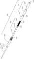
图1是本发明探针较佳实施方式的立体分解图。Fig. 1 is an exploded perspective view of a preferred embodiment of the probe of the present invention.
图2是图1中绝缘管的剖视图。Fig. 2 is a cross-sectional view of the insulating tube in Fig. 1 .
图3是图1的组装图。FIG. 3 is an assembly view of FIG. 1 .
图4是图3的剖视图。FIG. 4 is a sectional view of FIG. 3 .
图5是图1中的滤波单元的等效电路图。FIG. 5 is an equivalent circuit diagram of the filtering unit in FIG. 1 .
具体实施方式Detailed ways
请参考图1及图2,本发明探针10的较佳实施方式包括一滤波单元100及一针体200。所述滤波单元100包括一电感性组件120、一电容性组件160及一绝缘管180。Please refer to FIG. 1 and FIG. 2 , a preferred embodiment of the probe 10 of the present invention includes a
所述电感性组件120具有电感的特性,其包括一磁性体122、一导电线圈124及一绝缘介质管128。所述导电线圈124的两端分别设有两接触部125、126。在本实施方式中,所述磁性体122由磁性材料(如铁、钴、镍等)制成,且呈实心圆柱体状。所述导电线圈124具有弹性且呈圆形螺旋状,所述接触部125、126为分别自所述导电线圈124的两端向所述导电线圈124的中心轴垂直延伸出的两圆形导电片。在其它实施方式中,所述磁性体122可为中空或实心的其它形状(如长方体状、三角柱状等),所述导电线圈124的螺旋形状可根据所述磁性体122的形状而进行相应调整。The
所述电容性组件160具有电容的特性,其包括一金属内管162、一金属外管164及一绝缘介质管166。所述金属内管162的一端设有一接触部163,所述金属外管164的一端设有一挡止部165。在本实施方式中,所述金属内管162作为所述电容性组件160的高电位部,所述金属外管164作为所述电容性组件160的低电位部,且所述金属内管162及所述金属外管164均为中空圆柱体。所述挡止部165为自所述金属外管164一端的边缘向所述金属外管164的中心轴垂直延伸出的一C形金属挡片。所述接触部163为自所述C形金属缘的开口处所对应的所述金属内管162一端的边缘向所述金属内管162的中心轴垂直延伸出的一圆形金属片。所述金属内管162的内表面上设有螺纹。在其它实施方式中,所述金属内管162与所述金属外管164的形状及电位可根据实际需要而作相应调整。The
所述绝缘管180包括一收容腔181、一设于所述收容腔181内的颈缩部182及两开口183、184。在本实施方式中,所述绝缘管180用于对所述电感性组件120及所述电容性组件160进行电气隔离,其为一中空圆柱体,其内环半径大于所述导电线圈124的半径,其长度大于所述电感性组件120的长度。所述绝缘管180外表面上靠近所述开口184的一段区域内设有螺纹,用于与所述金属内管162内表面上的螺纹相配合,以将所述绝缘管180旋入所述金属内管162内,从而使所述电容性组件160螺旋锁固在所述绝缘管180上。所述绝缘管180的厚度大于所述绝缘介质管128、166的厚度。所述绝缘管180及所述绝缘介质管128、166均由玻璃纤维环氧化树脂(FR4)材料组成。The
所述针体200可穿置入所述绝缘管180的收容腔181,其包括一尖端部210及设于尖端部210后端的一抵靠部220。所述尖端部210的外径小于所述开口183的内径以使所述尖端部210可以从开口183伸出,所述抵靠部220的外径略大于所述开口183的内径,以使所述针体200在受到所述导电线圈124弹力的作用下,不会脱离所述绝缘管180。The
请参考图3及图4,组装时,所述绝缘介质管128套设在所述磁性体122上,所述导电线圈124呈螺旋状环绕在所述绝缘介质管128的外表面。所述绝缘介质管166具有粘性且套设在所述金属内管162外,所述金属外管164套设在所述绝缘介质管166外,并通过所述绝缘介质管166与所述金属内管162粘和在一起且又相互电气隔离。将所述针体200及所述电感性组件120自所述开口184穿置于所述收容腔181内,并将所述电容性组件160螺旋锁固在所述绝缘管180上。所述尖端部210从所述开口183伸出,用于接触一测试点(图未示)。所述抵靠部220的底部与所述接触部125接触,以实现所述针体200与所述电感性组件120的电连接,且所述抵靠部220由于受到所述导电线圈124弹力的作用而抵压所述颈缩部182。所述接触部126与所述接触部163接触,以实现所述电感性组件120与所述电容性组件160的电连接,所述挡止部165与所述金属内管162及所述绝缘管180的一端接触,用于阻挡所述金属内管162及所述绝缘管180。Please refer to FIG. 3 and FIG. 4 , during assembly, the
请继续参考图5,所述滤波单元100可等效为相互串联的一电感L及一电容C,所述电容C的一端接地,另一端与所述电感L的一端相连,所述电感L另一端与一测试设备(图未示)相连。因此,所述滤波单元100具有低通滤波器的特性。Please continue to refer to FIG. 5, the
当所述测试设备利用所述探针10对一电路板(图未示)上一测试点输出的待测信号进行测试时,所述尖端部210接触所述测试点,所述待测信号经所述针体200传输到所述滤波单元100,经所述滤波单元100滤除高频杂波后再传输给所述测试设备,以使所述测试设备对所述待测信号进行准确地测量。在本实施方式中,由于所述导电线圈124具有弹性,当所述探针10与所述电路板之间出现过度挤压时,所述导电线圈124可收缩,所述尖端部210可向所述收容腔181内移动,从而避免了因压力过大而导致的所述尖端部210或所述电路板的损坏。When the test equipment uses the probe 10 to test the signal to be tested outputted by a test point on a circuit board (not shown), the
所述探针10的滤波效果可通过改变所述滤波器单元100中的每一组件的参数来实现,例如,改变每一组件的材料、所述磁性体128的直径大小、所述导电线圈124的疏密、所述绝缘介质管128、166的厚度、所述绝缘管180的厚度等都可以改变所述探针10的滤波效果。当需要替换或调整所述滤波器单元100中的任一组件时,只需将所述绝缘管180从所述金属内管162中旋出,便可拆解所述滤波单元100,并根据需要重组所述滤波单元100内的各组件,以达到不同的滤波效果。The filtering effect of the probe 10 can be realized by changing the parameters of each component in the
所述探针10通过装设所述电感性组件120及所述电容性组件160来实现滤波的功能;并利用所述所述导电线圈124的弹性避免了测试时因压力过大而造成的损坏;且结构简单、便于拆卸与组装,从而可在需要时对所述滤波单元100进行组件的重组,以使所述探针10能满足不同的滤波需求。The probe 10 realizes the function of filtering by installing the
Claims (8)
Priority Applications (2)
| Application Number | Priority Date | Filing Date | Title |
|---|---|---|---|
| CN200910306443.2ACN102004173B (en) | 2009-09-01 | 2009-09-01 | probe |
| US12/752,138US8283939B2 (en) | 2009-09-01 | 2010-04-01 | Test probe |
Applications Claiming Priority (1)
| Application Number | Priority Date | Filing Date | Title |
|---|---|---|---|
| CN200910306443.2ACN102004173B (en) | 2009-09-01 | 2009-09-01 | probe |
Publications (2)
| Publication Number | Publication Date |
|---|---|
| CN102004173A CN102004173A (en) | 2011-04-06 |
| CN102004173Btrue CN102004173B (en) | 2014-02-19 |
Family
ID=43623903
Family Applications (1)
| Application Number | Title | Priority Date | Filing Date |
|---|---|---|---|
| CN200910306443.2AExpired - Fee RelatedCN102004173B (en) | 2009-09-01 | 2009-09-01 | probe |
Country Status (2)
| Country | Link |
|---|---|
| US (1) | US8283939B2 (en) |
| CN (1) | CN102004173B (en) |
Families Citing this family (16)
| Publication number | Priority date | Publication date | Assignee | Title |
|---|---|---|---|---|
| FR2947633B1 (en)* | 2009-07-02 | 2012-04-13 | Snecma | DEVICE FOR NON-DESTRUCTIVE CONTROL OF A PIECE |
| US20130328549A1 (en)* | 2012-06-07 | 2013-12-12 | Chung Instrument Electronics Industrial Co., Ltd. | Rotating mobile probe and probing rod using the same |
| JP2016205906A (en)* | 2015-04-17 | 2016-12-08 | 株式会社東芝 | Probe, semiconductor inspection apparatus, probe manufacturing method, semiconductor inspection apparatus manufacturing method, semiconductor inspection method, and semiconductor manufacturing method |
| JP2017142080A (en)* | 2016-02-08 | 2017-08-17 | 日本電産リード株式会社 | Contact terminal, inspection tool, and inspection device |
| CN106093752B (en)* | 2016-06-20 | 2019-03-12 | 定颖电子(黄石)有限公司 | A kind of test probe card applied to integrated circuit |
| USD869305S1 (en)* | 2017-02-10 | 2019-12-10 | Kabushiki Kaisha Nihon Micronics | Probe pin |
| JP1592871S (en)* | 2017-02-10 | 2017-12-11 | ||
| KR101954086B1 (en)* | 2017-11-07 | 2019-03-06 | 리노공업주식회사 | A test probe assembly and test socket |
| JP1626668S (en)* | 2018-02-02 | 2019-03-18 | ||
| JP1622968S (en)* | 2018-02-02 | 2019-01-28 | ||
| TWD197822S (en)* | 2018-02-02 | 2019-06-01 | Nihon Micronics Kk | Part of electric contact |
| JP1622970S (en)* | 2018-02-02 | 2019-01-28 | ||
| JP1622969S (en)* | 2018-02-02 | 2019-01-28 | ||
| JP1623280S (en)* | 2018-02-02 | 2019-01-28 | ||
| JP1626667S (en)* | 2018-02-02 | 2019-03-18 | ||
| JP1623279S (en)* | 2018-02-02 | 2019-01-28 |
Citations (3)
| Publication number | Priority date | Publication date | Assignee | Title |
|---|---|---|---|---|
| US3893027A (en)* | 1974-06-10 | 1975-07-01 | Tektronix Inc | Electrical test probe |
| CN1238571A (en)* | 1998-01-20 | 1999-12-15 | 株式会社村田制作所 | Dielectric filter and dielectric duplexer |
| US6404396B1 (en)* | 1999-03-12 | 2002-06-11 | Thomson-Csf | Dismantling-type antenna, with capacitive load, of whip type, and method of manufacturing a radiating segment of such an antenna |
Family Cites Families (11)
| Publication number | Priority date | Publication date | Assignee | Title |
|---|---|---|---|---|
| US4764722A (en)* | 1985-10-28 | 1988-08-16 | International Business Machines Corporation | Coaxial probe |
| US5136237A (en)* | 1991-01-29 | 1992-08-04 | Tektronix, Inc. | Double insulated floating high voltage test probe |
| US5235268A (en)* | 1991-11-13 | 1993-08-10 | Harthcock Jerry D | Test and measurement system |
| US6175228B1 (en)* | 1998-10-30 | 2001-01-16 | Agilent Technologies | Electronic probe for measuring high impedance tri-state logic circuits |
| US6218910B1 (en)* | 1999-02-25 | 2001-04-17 | Formfactor, Inc. | High bandwidth passive integrated circuit tester probe card assembly |
| US6466000B1 (en)* | 2000-05-31 | 2002-10-15 | Tektronix, Inc. | Replaceable probe tip holder and measurement probe head |
| US6700397B2 (en)* | 2000-07-13 | 2004-03-02 | The Micromanipulator Company, Inc. | Triaxial probe assembly |
| US6688906B2 (en)* | 2002-05-28 | 2004-02-10 | Agilent Technologies Inc. | Probes and methods for testing electrical circuits |
| TWI229188B (en)* | 2004-01-08 | 2005-03-11 | Asustek Comp Inc | Testing probe and testing jig |
| JP5080459B2 (en)* | 2005-06-13 | 2012-11-21 | カスケード マイクロテック インコーポレイテッド | Wideband active / passive differential signal probe |
| EP2180326B1 (en)* | 2008-10-24 | 2017-05-03 | Tyco Electronics Services GmbH | Test probe |
- 2009
- 2009-09-01CNCN200910306443.2Apatent/CN102004173B/ennot_activeExpired - Fee Related
- 2010
- 2010-04-01USUS12/752,138patent/US8283939B2/ennot_activeExpired - Fee Related
Patent Citations (3)
| Publication number | Priority date | Publication date | Assignee | Title |
|---|---|---|---|---|
| US3893027A (en)* | 1974-06-10 | 1975-07-01 | Tektronix Inc | Electrical test probe |
| CN1238571A (en)* | 1998-01-20 | 1999-12-15 | 株式会社村田制作所 | Dielectric filter and dielectric duplexer |
| US6404396B1 (en)* | 1999-03-12 | 2002-06-11 | Thomson-Csf | Dismantling-type antenna, with capacitive load, of whip type, and method of manufacturing a radiating segment of such an antenna |
Also Published As
| Publication number | Publication date |
|---|---|
| US20110050261A1 (en) | 2011-03-03 |
| CN102004173A (en) | 2011-04-06 |
| US8283939B2 (en) | 2012-10-09 |
Similar Documents
| Publication | Publication Date | Title |
|---|---|---|
| CN102004173B (en) | probe | |
| TWI512300B (en) | Cantilever high frequency probe card | |
| RU2509309C2 (en) | Capacitance sensor (versions) | |
| CN105823493A (en) | Sensitivity enhancement type eddy current transducer | |
| KR20210060597A (en) | Probe | |
| CN113167815A (en) | probe unit | |
| CN111566459B (en) | Probe unit | |
| CN205263204U (en) | Transient state electric -field sensor | |
| CN101689695A (en) | A TEM mode resonator | |
| CN105527505A (en) | Vibration capacitance type electrostatic sensor | |
| TW201109671A (en) | Probe | |
| CN205388617U (en) | Low pressure arm of dual -purpose type divider | |
| CN102801014B (en) | Connector socket used for eddy current testing device | |
| CN202178471U (en) | Cable connector for built-in coupler and coupler thereof | |
| CN204203301U (en) | A kind of simple and easy radio frequency testing pen | |
| CA2677775A1 (en) | Apparatus for determining and/or monitoring a process variable | |
| CN203643559U (en) | Sensing device for detecting partial discharge inside GIS through UHF method | |
| TWI522621B (en) | Test fixture | |
| CN104714055B (en) | Detection jig | |
| WO2015049725A1 (en) | Partial discharge sensor | |
| CN102006025B (en) | Filter | |
| JP6118710B2 (en) | Probe card | |
| CN101997505A (en) | filter | |
| CN219831286U (en) | Partial discharge sensor mounted on distribution transformer oil level gauge | |
| CN108508066B (en) | Capacitance probe |
Legal Events
| Date | Code | Title | Description |
|---|---|---|---|
| C06 | Publication | ||
| PB01 | Publication | ||
| C10 | Entry into substantive examination | ||
| SE01 | Entry into force of request for substantive examination | ||
| C14 | Grant of patent or utility model | ||
| GR01 | Patent grant | ||
| ASS | Succession or assignment of patent right | Owner name:NANTONG MEDICAL APPARATUS CO., LTD. Free format text:FORMER OWNER: BEIJING ZHONGCAI WYSE EDUCATION TECHNOLOGY CO., LTD. Effective date:20141203 Free format text:FORMER OWNER: HONGFUJIN PRECISE INDUSTRY CO., LTD. Effective date:20141203 Owner name:BEIJING ZHONGCAI WYSE EDUCATION TECHNOLOGY CO., LT Free format text:FORMER OWNER: HONGFUJIN PRECISE INDUSTRY (SHENZHEN) CO., LTD. Effective date:20141203 | |
| C41 | Transfer of patent application or patent right or utility model | ||
| COR | Change of bibliographic data | Free format text:CORRECT: ADDRESS; FROM: 100083 HAIDIAN, BEIJING TO: 226351 NANTONG, JIANGSU PROVINCE Free format text:CORRECT: ADDRESS; FROM: 518109 SHENZHEN, GUANGDONG PROVINCE TO: 100083 HAIDIAN, BEIJING | |
| TR01 | Transfer of patent right | Effective date of registration:20141203 Address after:226351, No. 84 East Main Street, stone port town, Nantong, Jiangsu, Tongzhou District Patentee after:NANTONG MEDICAL APPARATUS Co.,Ltd. Address before:100083 Beijing Haidian District Zhongguancun Road No. 18 smartfortune International Building B706 Patentee before:Beijing Zhongcai Wyse Education Technology Co.,Ltd. Effective date of registration:20141203 Address after:100083 Beijing Haidian District Zhongguancun Road No. 18 smartfortune International Building B706 Patentee after:Beijing Zhongcai Wyse Education Technology Co.,Ltd. Address before:518109 Guangdong city of Shenzhen province Baoan District Longhua Town Industrial Zone tabulaeformis tenth East Ring Road No. 2 two Patentee before:HONG FU JIN PRECISION INDUSTRY (SHENZHEN) Co.,Ltd. Patentee before:HON HAI PRECISION INDUSTRY Co.,Ltd. | |
| C56 | Change in the name or address of the patentee | ||
| CP02 | Change in the address of a patent holder | Address after:226351, No. 68, South District, Tongzhou District port town, Nantong, Jiangsu Patentee after:NANTONG MEDICAL APPARATUS Co.,Ltd. Address before:226351, No. 84 East Main Street, stone port town, Nantong, Jiangsu, Tongzhou District Patentee before:NANTONG MEDICAL APPARATUS Co.,Ltd. | |
| CF01 | Termination of patent right due to non-payment of annual fee | Granted publication date:20140219 Termination date:20180901 | |
| CF01 | Termination of patent right due to non-payment of annual fee |