CN101989854B - Load driving device - Google Patents
Load driving deviceDownload PDFInfo
- Publication number
- CN101989854B CN101989854BCN 200910159032CN200910159032ACN101989854BCN 101989854 BCN101989854 BCN 101989854BCN 200910159032CN200910159032CN 200910159032CN 200910159032 ACN200910159032 ACN 200910159032ACN 101989854 BCN101989854 BCN 101989854B
- Authority
- CN
- China
- Prior art keywords
- current
- voltage
- load
- reference signal
- signal
- Prior art date
- Legal status (The legal status is an assumption and is not a legal conclusion. Google has not performed a legal analysis and makes no representation as to the accuracy of the status listed.)
- Active
Links
- 238000006243chemical reactionMethods0.000claimsdescription43
- 230000007274generation of a signal involved in cell-cell signalingEffects0.000claimsdescription8
- 230000000052comparative effectEffects0.000claims4
- 230000026683transductionEffects0.000claims1
- 238000010361transductionMethods0.000claims1
- 239000003990capacitorSubstances0.000description30
- 238000010586diagramMethods0.000description16
- 101100464779Saccharomyces cerevisiae (strain ATCC 204508 / S288c) CNA1 geneProteins0.000description9
- 238000000034methodMethods0.000description2
- 238000012986modificationMethods0.000description2
- 230000004048modificationEffects0.000description2
- 230000000694effectsEffects0.000description1
- 230000000087stabilizing effectEffects0.000description1
Images


Landscapes
- Dc-Dc Converters (AREA)
Abstract
Translated fromChinese
Description
Translated fromChinese技术领域technical field
本发明涉及一种负载驱动装置。The invention relates to a load driving device.
背景技术Background technique
在现有的技术领域中的负载驱动装置中,常因为负载驱动装置所接收的输入电压有涟波(ripple)的现象,而导致其所传送以驱动负载的电气信号也同样具有涟波的现象。如此一来,负载所接收的电气信号会产生不足的现象而减低了整体的效率。In the load driving device in the existing technical field, often because the input voltage received by the load driving device has a ripple phenomenon, the electrical signal transmitted by it to drive the load also has a ripple phenomenon. . In this way, the electrical signal received by the load will be insufficient and reduce the overall efficiency.
因此,现有技术提出了一种负载驱动装置来解决上述的问题。请参照图1,图1所示为现有的驱动器的示意图。其中驱动器110接收输入电压VIN并传送电气信号IV至负载120。并且,驱动器110还由负载120上侦测到反馈信号FB来做为动态调整电气信号IV的依据。Therefore, the prior art proposes a load driving device to solve the above problems. Please refer to FIG. 1 , which is a schematic diagram of an existing driver. The
然而,这种现有的驱动器110所接收的反馈信号FB通常是负载120所接收的电气信号IV的峰值,但系统设计时,负载120的最佳设定值一般是由平均电压值或平均电流值来表示,因此,前述的反馈控制方式并不合乎需求,可能使得实际驱动负载120的电气信号IV的平均值会低于负载120原本设计所须的最佳设定值,严重的降低负载120所能产生的效能。However, the feedback signal FB received by the existing
发明内容Contents of the invention
本发明提供一种负载驱动装置,其所提供用以驱动负载的电气信号的平均值等于负载的需求。The invention provides a load driving device, the average value of the electrical signal provided by it to drive the load is equal to the demand of the load.
本发明提出一种负载驱动装置,用以输出电气信号至负载。负载驱动装置包括驱动器以及平均电压电流侦测器。驱动器耦接负载,接收输入电压及控制信号。驱动器依据控制信号以调整所输出的电气信号。平均电压电流侦测器耦接驱动器及负载,接收流至负载的电气信号,并利用电气信号与参考信号进行比对以产生控制信号。The invention provides a load driving device for outputting electrical signals to the load. The load driving device includes a driver and an average voltage and current detector. The driver is coupled to the load and receives the input voltage and the control signal. The driver adjusts the output electrical signal according to the control signal. The average voltage and current detector is coupled to the driver and the load, receives the electrical signal flowing to the load, and compares the electrical signal with a reference signal to generate a control signal.
在本发明的一实施例中,上述的驱动器为电源转换器In one embodiment of the present invention, the above-mentioned driver is a power converter
在本发明的一实施例中,上述的电气信号为驱动电流In one embodiment of the present invention, the electrical signal mentioned above is the driving current
在本发明的一实施例中,上述的平均电压电流侦测器包括电流感测器、电流电压转换器以及比较器。电流感测器耦接负载,用以感测驱动电流。电流电压转换器耦接电流感测器,用以转换感测到的驱动电流为比较电压。比较器耦接电流感测器及电流电压转换器,用以比较参考信号及比较电压,并藉以产生控制信号。In an embodiment of the present invention, the above-mentioned average voltage and current detector includes a current sensor, a current-to-voltage converter, and a comparator. The current sensor is coupled to the load for sensing the driving current. The current-to-voltage converter is coupled to the current sensor for converting the sensed driving current into a comparison voltage. The comparator is coupled to the current sensor and the current-to-voltage converter, and is used for comparing the reference signal and the comparison voltage to generate a control signal.
在本发明的一实施例中,上述的电流电压转换器为转换电阻,其一端接收驱动电流,另一端耦接接地电压。In an embodiment of the present invention, the above-mentioned current-to-voltage converter is a switching resistor, one end of which receives the driving current, and the other end is coupled to the ground voltage.
在本发明的一实施例中,上述的比较器为运算转导放大器(Operational Transconductance Amplifier,OTA)。In an embodiment of the present invention, the above-mentioned comparator is an operational transconductance amplifier (Operational Transconductance Amplifier, OTA).
在本发明的一实施例中,负载驱动装置还包括参考信号产生电路,用以产生参考信号。参考信号产生电路则包括参考电流源以及参考电阻。参考电流源耦接至比较器并提供参考电流。参考电阻的一端接收参考电流并产生参考信号,其另一端耦接接地电压。In an embodiment of the present invention, the load driving device further includes a reference signal generating circuit for generating the reference signal. The reference signal generating circuit includes a reference current source and a reference resistor. The reference current source is coupled to the comparator and provides a reference current. One end of the reference resistor receives a reference current and generates a reference signal, and the other end of the reference resistor is coupled to a ground voltage.
在本发明的一实施例中,上述的电流电压转换器包括第一转换电容以及第一转换开关。第一转换电容的一端接收驱动电流,另一端耦接接地电压。第一转换开关则与第一转换电容并连耦接。In an embodiment of the present invention, the above-mentioned current-to-voltage converter includes a first conversion capacitor and a first conversion switch. One end of the first conversion capacitor receives the driving current, and the other end is coupled to the ground voltage. The first transfer switch is coupled in parallel with the first transfer capacitor.
在本发明的一实施例中,上述的负载驱动装置还包括参考信号产生电路用以产生参考信号。参考信号产生电路包括参考电流源、第二转换电容以及第二转换开关。参考电流源耦接至比较器,提供参考电流。第二转换电容的一端接收参考电流,另一端耦接接地电压。第二转换开关与第二转换电容并连耦接。In an embodiment of the present invention, the above-mentioned load driving device further includes a reference signal generating circuit for generating the reference signal. The reference signal generation circuit includes a reference current source, a second switching capacitor and a second switching switch. The reference current source is coupled to the comparator to provide a reference current. One end of the second conversion capacitor receives the reference current, and the other end is coupled to the ground voltage. The second transfer switch is coupled in parallel with the second transfer capacitor.
在本发明的一实施例中,上述的电气信号为驱动电压。In an embodiment of the present invention, the electrical signal mentioned above is a driving voltage.
在本发明的一实施例中,上述的平均电压电流侦测器包括第一电压电流转换器、电流电压转换器以及比较器。第一电压电流转换器耦接负载,用以接收并转换驱动电压以产生转换电流。电流电压转换器耦接第一电压电流转换器,用以将转换电流转换为比较电压。比较器耦接第一电压电流转换器及电流电压转换器,用以比较参考信号及比较电压并藉以产生控制信号。In an embodiment of the present invention, the above-mentioned average voltage and current detector includes a first voltage-to-current converter, a current-to-voltage converter and a comparator. The first voltage-to-current converter is coupled to the load for receiving and converting the driving voltage to generate a converted current. The current-to-voltage converter is coupled to the first voltage-to-current converter for converting the conversion current into a comparison voltage. The comparator is coupled to the first voltage-to-current converter and the current-to-voltage converter, and is used for comparing the reference signal and the comparison voltage to generate a control signal.
在本发明的一实施例中,上述的电流电压转换器为转换电阻,其一端接收转换电流,另一端耦接接地电压。In an embodiment of the present invention, the above-mentioned current-to-voltage converter is a conversion resistor, one end of which receives the conversion current, and the other end is coupled to the ground voltage.
在本发明的一实施例中,上述的负载驱动装置其中还包括参考信号产生电路,用以产生该参考信号。参考信号产生电路包括第二电压电流转换器以及参考电阻。第二电压电流转换器耦接至比较器,接收参考电压并转换参考电压以产生参考电流。参考电阻的一端接收参考电流并产生参考信号,其另一端耦接接地电压。In an embodiment of the present invention, the above-mentioned load driving device further includes a reference signal generating circuit for generating the reference signal. The reference signal generating circuit includes a second voltage-current converter and a reference resistor. The second voltage-to-current converter is coupled to the comparator, receives the reference voltage and converts the reference voltage to generate a reference current. One end of the reference resistor receives a reference current and generates a reference signal, and the other end of the reference resistor is coupled to a ground voltage.
在本发明的一实施例中,上述的电流电压转换器包括第一转换电容以及第一转换开关。第一转换电容的一端接收驱动电流,另一端耦接接地电压。第一转换开关则与第一转换电容并连耦接In an embodiment of the present invention, the above-mentioned current-to-voltage converter includes a first conversion capacitor and a first conversion switch. One end of the first conversion capacitor receives the driving current, and the other end is coupled to the ground voltage. The first transfer switch is coupled in parallel with the first transfer capacitor
在本发明的一实施例中,上述的负载驱动装置还包括一参考信号产生电路,用以产生该参考信号,包括第二电压电流转换器、第二转换电容以及第二转换开关。第二电压电流转换器耦接至比较器,接收参考电压并转换参考电压以产生参考电流。第二转换电容的一端接收参考电流,另一端耦接接地电压。第二转换开关与第二转换电容并连耦接。In an embodiment of the present invention, the above-mentioned load driving device further includes a reference signal generation circuit for generating the reference signal, including a second voltage-to-current converter, a second conversion capacitor and a second transfer switch. The second voltage-to-current converter is coupled to the comparator, receives the reference voltage and converts the reference voltage to generate a reference current. One end of the second conversion capacitor receives the reference current, and the other end is coupled to the ground voltage. The second transfer switch is coupled in parallel with the second transfer capacitor.
在本发明的一实施例中,上述的负载驱动装置还包括缓冲器,串接在比较器接收驱动电压的路径上。In an embodiment of the present invention, the above-mentioned load driving device further includes a buffer connected in series on the path where the comparator receives the driving voltage.
在本发明的一实施例中,上述的平均电压电流侦测器包括比较器。比较器接收驱动电压及参考信号,并比较参考信号及驱动电压,藉以产生控制信号。其中,参考信号为电压信号。In an embodiment of the present invention, the above-mentioned average voltage and current detector includes a comparator. The comparator receives the driving voltage and the reference signal, and compares the reference signal and the driving voltage to generate a control signal. Wherein, the reference signal is a voltage signal.
基于上述,本发明反馈负载上的电气信号(电流或电压),并使电气信号与参考信号进行比对,来藉以调整负载驱动装置的电气信号的输出。使负载驱动装置所输出的电气信号的平均值可以接近负载所需要的值,进而提升负载驱动装置的效能。Based on the above, the present invention feeds back the electrical signal (current or voltage) on the load, and compares the electrical signal with the reference signal to adjust the output of the electrical signal of the load driving device. The average value of the electrical signal output by the load driving device can be close to the value required by the load, thereby improving the performance of the load driving device.
下面通过附图和实施例,对本发明的技术方案做进一步的详细描述。The technical solutions of the present invention will be described in further detail below with reference to the accompanying drawings and embodiments.
附图说明Description of drawings
图1所示为现有的驱动器的示意图;Figure 1 is a schematic diagram of an existing driver;
图2所示为本发明的第一实施例的负载驱动装置的示意图;FIG. 2 is a schematic diagram of a load driving device according to a first embodiment of the present invention;
图3所示为本发明的第二实施例的负载驱动装置的示意图;FIG. 3 is a schematic diagram of a load driving device according to a second embodiment of the present invention;
图4所示为本发明的第三实施例的负载驱动装置的示意图;FIG. 4 is a schematic diagram of a load driving device according to a third embodiment of the present invention;
图5所示为图4的实施例的动作波形图;Fig. 5 shows the action waveform diagram of the embodiment of Fig. 4;
图6所示为本发明的第四实施例的负载驱动装置的示意图;FIG. 6 is a schematic diagram of a load driving device according to a fourth embodiment of the present invention;
图7所示为本发明的第五实施例的负载驱动装置的示意图;FIG. 7 is a schematic diagram of a load driving device according to a fifth embodiment of the present invention;
图8所示为本发明的第六实施例的负载驱动装置的示意图。FIG. 8 is a schematic diagram of a load driving device according to a sixth embodiment of the present invention.
主要元件符号说明Description of main component symbols
110、210:驱动器; 120、230、330、430、630、830:110, 210: drive; 120, 230, 330, 430, 630, 830:
负载;load;
200:负载驱动装置; 220、320、420、620、820:平均电200: load driving device; 220, 320, 420, 620, 820: average current
压电流侦测器;piezo current detector;
310、410、610、810:电源转换器; 321、421:电流感测器;310, 410, 610, 810: power converter; 321, 421: current sensor;
322、422、622:参考信号产生电路; 323、423、623、723:电流电压转322, 422, 622: reference signal generation circuit; 323, 423, 623, 723: current voltage conversion
换器;Converter;
621,6221:电压电流转换器; 821:缓冲器;621, 6221: voltage-current converter; 821: buffer;
ISENSE、Iref:电流; RST:重置信号;ISENSE, Iref: current; RST: reset signal;
CMP1:比较器; IV:电气信号;CMP1: comparator; IV: electrical signal;
VIN:输入电压; FB:反馈信号;VIN: input voltage; FB: feedback signal;
CTRL:控制信号; Vref:参考信号;CTRL: control signal; Vref: reference signal;
R1、R2:电阻; C1~C3:电容;R1, R2: resistance; C1~C3: capacitance;
SW1、SW2:开关; GND:接地电压;SW1, SW2: switch; GND: ground voltage;
V+、V-、VR: 电压;REF:电流源;V+, V-, VR: voltage; REF: current source;
T1:时间点。T1: point in time.
具体实施方式Detailed ways
请参照图2,图2所示为本发明第一实施例的负载驱动装置的示意图。其中,负载驱动装置200连接负载230并输出电气信号IV以驱动负载230。负载驱动装置200包括驱动器210及平均电压电流侦测器220。驱动器210与负载230及平均电压电流侦测器220相耦接,驱动器210接收输入电压VIN及控制信号CTRL。而电气信号IV即是由驱动器210所输出,并且,驱动器210依据控制信号CTRL来调整其所输出的电气信号IV。Please refer to FIG. 2 , which is a schematic diagram of a load driving device according to a first embodiment of the present invention. Wherein, the
驱动器210可以由电源转换器(power converter)来建构。也就是说,驱动器210可以是电压转换器或是电流转换器中的一种。而这种电源转换器会依据其所接收的输入电压VIN来产生输出的电气信号IV。在此所述的电源转换器为本领域技术人员都熟知的电路,其工作细节此处不多详述。The
平均电压电流侦测器220同样也与负载230耦接,并由负载230接收电气信号IV。平均电压电流侦测器220则是依据其所接收的电气信号IV与参考信号来进行比较,再藉由比较的结果来产生控制信号CTRL。The average voltage and
在此,电气信号IV可以是用来驱动负载230的驱动电流或是驱动电压。电气信号IV的形式可以由负载230是为电流驱动或是电压驱动的方式来决定,当负载230是为电流驱动时,电气信号IV是驱动电流。相反的,当负载230是为电压驱动时,电气信号IV是驱动电压。Here, the electrical signal IV may be a driving current or a driving voltage for driving the
在此请注意,上述的参考信号则可以依据负载230所需要的电气信号IV的值来设定。以电气信号IV为驱动电压为例子,若是负载230所需要的最佳驱动电压为5伏特(volt,V),则参考信号可以依据5V来设定,例如设定为5V。Please note here that the above reference signal can be set according to the value of the electrical signal IV required by the
以下将针对电气信号IV的不同形式的不同的负载驱动装置的实施例来做介绍,使本领域技术人员更能清楚了解本发明,并具以实施。The following will introduce embodiments of different load driving devices in different forms of the electrical signal IV, so that those skilled in the art can better understand and implement the present invention.
请参照图3,图3所示为本发明第二实施例的负载驱动装置的示意图。负载驱动装置由电源转换器310及平均电压电流侦测器320所构成。电源转换器310接收控制信号CTRL并据以产生驱动电流形式的电气信号IV,用来驱动负载330。其中,平均电压电流侦测器320包括电流感测器321、电流电压转换器323、比较器CMP1以及参考信号产生电路322。Please refer to FIG. 3 , which is a schematic diagram of a load driving device according to a second embodiment of the present invention. The load driving device is composed of a
电流感测器321与负载330耦接,电流感测器321接收驱动电流形式的电气信号IV,并传送感测到的驱动电流ISENSE通过电流电压转换器323。电流电压转换器323由转换电阻R1所建构。转换电阻R1串接在电流感测器321与接地电压GND间,转换电阻R1的一端接收感测到的驱动电流ISENSE而另一端则连接接地电压GND。当感测到的驱动电流ISENSE流过转换电阻R1时,会在转换电阻R1接收感测到的驱动电流ISENSE的端点上产生比较电压V-。The
另外,参考信号V+可以藉由参考信号产生电路322来产生。在本实施例中,参考信号产生电路322包括参考电流源REF以及参考电阻R2。参考电阻R2的一端接收参考电流源REF所提供的参考电流Iref,而参考电阻R2的另一端则连接至接地电压GND。在参考电流通过参考电阻R2时,参考电阻R2连接参考电流源REF的端点上即产生参考信号V+。In addition, the reference signal V+ can be generated by the reference
比较器CMP1则接收参考信号V+以及比较电压V-,并依据比较参考信号V+以及比较电压V-来产生控制信号CTRL。此外,比较器CMP1输出控制信号CTRL的端点上,可以串接一个稳压电容C1至接地电压GND。在本实施例中,比较器CMP1是利用运算放大器来建构。当然,比较器CMP1也可以利用运算转导放大器(Operational TransconductanceAmplifier,OTA)来建构。The comparator CMP1 receives the reference signal V+ and the comparison voltage V−, and generates the control signal CTRL according to the comparison reference signal V+ and the comparison voltage V−. In addition, a terminal of the comparator CMP1 outputting the control signal CTRL may be connected in series with a voltage stabilizing capacitor C1 to the ground voltage GND. In this embodiment, the comparator CMP1 is constructed by using an operational amplifier. Of course, the comparator CMP1 can also be constructed by using an operational transconductance amplifier (Operational Transconductance Amplifier, OTA).
由上述的说明可以得知,在经由比较器CMP1依据参考信号V+以及比较电压V-来改变其所产生的控制信号CTRL的情况下,电源转换器310所依据控制信号CTRL所产生的电气信号(驱动电流)IV的平均值就可以与负载330所需要的驱动电流相当接近,使负载330可以发挥其最大的功效。From the above description, it can be known that when the control signal CTRL generated by the comparator CMP1 is changed according to the reference signal V+ and the comparison voltage V−, the electrical signal generated by the
接着请参照图4,图4所示为本发明第三实施例的负载驱动装置的示意图。负载驱动装置由电源转换器410及平均电压电流侦测器420所构成。而电源转换器410耦接负载430并提供电气信号IV以驱动负载430。与上一实施例不同的是,本实施例中的平均电压电流侦测器420所包括的电流电压转换器423是利用转换电容C2以及转换开关SW1所建构的。其中转换电容C2与转换开关SW1相并连,而转换电容C2的一端接收感测到的驱动电流ISENSE而其另一端连接接地电压GND。Next please refer to FIG. 4 , which is a schematic diagram of a load driving device according to a third embodiment of the present invention. The load driving device is composed of a
转换开关SW1则受控于重置信号RST,当转换开关SW1依据重置信号RST而形成断路时,转换电容C2会接收驱动电流ISENSE而进行充电,因此,比较电压V-将会随着时间而升高。而当转换开关SW1依据重置信号RST而导通时,转换电容C2中的电荷将会漏出至接地电压GND,使得比较电压V-等于接地电压GND。The transfer switch SW1 is controlled by the reset signal RST. When the transfer switch SW1 is disconnected according to the reset signal RST, the transfer capacitor C2 will receive the driving current ISENSE to charge. Therefore, the comparison voltage V- will increase with time. raised. When the transfer switch SW1 is turned on according to the reset signal RST, the charges in the transfer capacitor C2 will leak to the ground voltage GND, so that the comparison voltage V− is equal to the ground voltage GND.
另外,本实施例中的参考信号产生电路422包括参考电流源REF外,还包括转换电容C3以及转换开关SW2。转换电容C3与转换开关SW2相并连,而转换电容C3的一端接收参考电流源REF所产生的参考电流Iref,而其另一端连接接地电压GND,转换开关SW2受控于重置信号RST。转换电容C3以及转换开关SW2与电流电压转换器323的动作方式相同,此处不多赘述。In addition, the reference
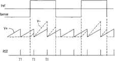
接着请参照图5,图5所示为图4实施例的动作波形图。其中当重置信号RST维持在低准位时,转换开关SW1、SW2保持断路,而比较电压V-及参考电压V+随着时间上升,一旦重置信号RST于时间点T1产生高准位突波时,转换电容C2、C3被瞬间放电而比较电压V-及参考电压V+皆被重置为零准位。Next, please refer to FIG. 5 , which is an action waveform diagram of the embodiment in FIG. 4 . Wherein, when the reset signal RST is maintained at a low level, the transfer switches SW1 and SW2 are kept open, while the comparison voltage V- and the reference voltage V+ increase with time, once the reset signal RST generates a high level surge at time point T1 , the switching capacitors C2 and C3 are discharged instantaneously and the comparison voltage V- and the reference voltage V+ are both reset to zero level.
此外,由图5所示可以得知,当比较电压V-低于参考电压V+时,表示驱动电流ISENSE低于参考电流Iref。此时电源转换器410依据控制信号CTRL调高驱动电流ISENSE。相反的,当比较电压V-高于参考电压V+时,表示驱动电流ISENSE高于参考电流Iref。此时电源转换器410依据控制信号CTRL调低驱动电流ISENSE。如此一来,驱动电流ISENSE的平均值将会很接近参考电流Iref。In addition, it can be known from FIG. 5 that when the comparison voltage V- is lower than the reference voltage V+, it means that the driving current ISENSE is lower than the reference current Iref. At this time, the
请参照图6,图6所示为本发明的第四实施例的负载驱动装置的示意图。负载驱动装置由电源转换器610及平均电压电流侦测器620所构成。电源转换器610接收控制信号CTRL并据以产生驱动电压形式的电气信号IV,用来驱动负载630。其中,平均电压电流侦测器620包括电压电流转换器621、电流电压转换器623以及参考信号产生电路622。Please refer to FIG. 6 , which is a schematic diagram of a load driving device according to a fourth embodiment of the present invention. The load driving device is composed of a
电压电流转换器621接收驱动电压形式的电气信号IV,并转换电气信号IV而产生转换电流ISENSE。电流电压转换器623则可以由转换电阻R1来建构,其中转换电阻R1的一端接收转换电流ISENSE,而其另一端连接接地电压GND。The voltage-to-
参考信号产生电路622则包括电压电流转换器6221以及参考电阻R2。电压电流转换器6221接收参考电压VR并转换参考电压VR以产生参考电流Iref。参考电阻R2的一端接收参考电流Iref,而其另一端连接接地电压GND。The reference
本第四实施例的负载驱动装置的运作方式与前述的第二实施例的负载驱动装置是非常相似的。所存在的差别是在于本第四实施例的电源转换器610所产生的电气信号IV是驱动电压的形式。因此,在本第四实施例中,必须藉由电压电流转换器621将电气信号IV转换成转换电流ISENSE。而提供参考电流Iref的部份,也是利用提供参考电压VR并藉由电压电流转换器6221转换参考电压VR来获得参考电流Iref。而除了上述说明的差异外,本第四实施例的负载驱动装置的动作方式与第二实施例中所说明的均相同,此处不多赘述。The operation mode of the load driving device of the fourth embodiment is very similar to that of the load driving device of the second embodiment mentioned above. The difference is that the electrical signal IV generated by the
以下请参照图7,图7所示为本发明的第五实施例的负载驱动装置的示意图。本发明的第五实施例的负载驱动装置与前述第四实施例的负载驱动装置大致上是相同的。差别在于第四实施例中的转换电阻R1在本第五实施例中置换为转换电容C2及转换开关SW1所并连构成的电流电压转换器723。而参考信号产生电路中,第四实施例的参考电阻R2在本第五实施例被置换为转换电容C3及转换开关SW2。Please refer to FIG. 7 below. FIG. 7 is a schematic diagram of a load driving device according to a fifth embodiment of the present invention. The load driving device of the fifth embodiment of the present invention is substantially the same as the load driving device of the aforementioned fourth embodiment. The difference is that the conversion resistor R1 in the fourth embodiment is replaced by the current-to-
其中的转换电容C2的一端接收转换电流ISENSE而其另一端连接接地电压GND。而转换电容C3及转换开关SW2相互并连,且转换电容C3的一端接收参考电流Iref且其另一端连接接地电压GND。转换开关SW1、SW2皆受控于重置信号RST。关于转换电容C2、C3及转换开关SW1、SW2的动作细节在前述第三实施例中以有详细的说明,此处不再赘述。One end of the switching capacitor C2 receives the switching current ISENSE and the other end thereof is connected to the ground voltage GND. The conversion capacitor C3 and the conversion switch SW2 are connected in parallel, and one end of the conversion capacitor C3 receives the reference current Iref and the other end thereof is connected to the ground voltage GND. Both the transfer switches SW1 and SW2 are controlled by the reset signal RST. The operation details of the switching capacitors C2 , C3 and the switching switches SW1 , SW2 are described in detail in the aforementioned third embodiment, and will not be repeated here.
最后请参照图8,图8所示为本发明的第六实施例的负载驱动装置的示意图。负载驱动装置由电源转换器810及平均电压电流侦测器820所构成。电源转换器810依据控制信号CTRL产生驱动电压形式的电气信号IV来驱动负载830。平均电压电流侦测器820包括比较器CMP1,比较器CMP1可以直接接收电气信号IV以及参考信号Vref来进行比较并产生控制信号CTRL。在此,参考信号Vref是一个电压形式的电压信号。Finally, please refer to FIG. 8 , which is a schematic diagram of a load driving device according to a sixth embodiment of the present invention. The load driving device is composed of a
此外,在比较器CMP1接收电气信号IV的路径上,还可以串接缓冲器821,用以确保电气信号IV的稳定度。In addition, a
综上所述,本发明利用反馈负载上的电气信号,来与设定的参考信号进行比对,使得电气信号的平均值可以接近负载所需要的驱动信号的能量。有效提升负载的工作效能。To sum up, the present invention compares the electrical signal on the feedback load with the set reference signal, so that the average value of the electrical signal can be close to the energy of the driving signal required by the load. Effectively improve the working performance of the load.
最后应说明的是:以上实施例仅用以说明本发明的技术方案而非对其进行限制,尽管参照较佳实施例对本发明进行了详细的说明,本领域的普通技术人员应当理解:其依然可以对本发明的技术方案进行修改或者等同替换,而这些修改或者等同替换亦不能使修改后的技术方案脱离本发明技术方案的精神和范围。Finally, it should be noted that the above embodiments are only used to illustrate the technical solutions of the present invention and not to limit them. Although the present invention has been described in detail with reference to the preferred embodiments, those of ordinary skill in the art should understand that: it still Modifications or equivalent replacements can be made to the technical solutions of the present invention, and these modifications or equivalent replacements cannot make the modified technical solutions deviate from the spirit and scope of the technical solutions of the present invention.
Claims (7)
Priority Applications (1)
| Application Number | Priority Date | Filing Date | Title |
|---|---|---|---|
| CN 200910159032CN101989854B (en) | 2009-07-29 | 2009-07-29 | Load driving device |
Applications Claiming Priority (1)
| Application Number | Priority Date | Filing Date | Title |
|---|---|---|---|
| CN 200910159032CN101989854B (en) | 2009-07-29 | 2009-07-29 | Load driving device |
Publications (2)
| Publication Number | Publication Date |
|---|---|
| CN101989854A CN101989854A (en) | 2011-03-23 |
| CN101989854Btrue CN101989854B (en) | 2013-07-17 |
Family
ID=43746235
Family Applications (1)
| Application Number | Title | Priority Date | Filing Date |
|---|---|---|---|
| CN 200910159032ActiveCN101989854B (en) | 2009-07-29 | 2009-07-29 | Load driving device |
Country Status (1)
| Country | Link |
|---|---|
| CN (1) | CN101989854B (en) |
Families Citing this family (4)
| Publication number | Priority date | Publication date | Assignee | Title |
|---|---|---|---|---|
| CN102357034B (en)* | 2011-09-23 | 2013-01-23 | 中国人民解放军第四军医大学 | Low-power consumption current excitation source for electrical impedance imaging |
| TWI676886B (en)* | 2018-11-05 | 2019-11-11 | 廣達電腦股份有限公司 | System loading detecting device and method |
| US10838444B1 (en)* | 2019-07-25 | 2020-11-17 | Semiconductor Components Industries, Llc | Adaptive constant current engine |
| CN110601683B (en)* | 2019-08-19 | 2023-02-10 | 麦歌恩电子(上海)有限公司 | Switch control circuit and control method |
Citations (2)
| Publication number | Priority date | Publication date | Assignee | Title |
|---|---|---|---|---|
| CN1578095A (en)* | 2003-07-07 | 2005-02-09 | 罗姆股份有限公司 | Load driving device and its portable machine |
| US7064553B2 (en)* | 2003-10-15 | 2006-06-20 | Anden Co., Ltd. | Open-circuit detecting circuit |
- 2009
- 2009-07-29CNCN 200910159032patent/CN101989854B/enactiveActive
Patent Citations (2)
| Publication number | Priority date | Publication date | Assignee | Title |
|---|---|---|---|---|
| CN1578095A (en)* | 2003-07-07 | 2005-02-09 | 罗姆股份有限公司 | Load driving device and its portable machine |
| US7064553B2 (en)* | 2003-10-15 | 2006-06-20 | Anden Co., Ltd. | Open-circuit detecting circuit |
Also Published As
| Publication number | Publication date |
|---|---|
| CN101989854A (en) | 2011-03-23 |
Similar Documents
| Publication | Publication Date | Title |
|---|---|---|
| CN108777903B (en) | Current source circuit and LED driver circuit | |
| CN103187875B (en) | Switching power supply and its control circuit | |
| US8487601B2 (en) | Method and apparatus to control a power factor correction circuit | |
| CN101552560B (en) | Switch voltage stabilizing circuit and control method thereof | |
| TWI401555B (en) | Voltage-regulating circuit with input voltage detecting circuit and parallel voltage-regulating circuit system using the same | |
| TWI496402B (en) | Current-mode buck converter and electronic system using the same | |
| CN101174769B (en) | Self-recovery multifunctional protection circuit | |
| CN105048814B (en) | Flyback power supply and control circuit and control method thereof | |
| US20140035541A1 (en) | Control circuit, control method used in pfc circuit and power source system thereof | |
| CN100592237C (en) | Intelligent switching power supply power detection and control device | |
| TWI484739B (en) | Active power factor correction circuit and related pfc controller | |
| CN103683925B (en) | DC-DC controller | |
| CN103997206A (en) | Switching power source | |
| US9680369B2 (en) | Power factor correction circuit of power converter | |
| KR20140041108A (en) | Power supply circuit and hysteresis buck converter | |
| CN100438290C (en) | DC-DC converter and conversion device | |
| US20120299563A1 (en) | Power converter and control method using the same | |
| CN104283430B (en) | Soft start switching power supply conversion device | |
| TW200828004A (en) | Power supply system and method for controlling output voltage | |
| TW201025813A (en) | Voltage converters and voltage generating methods | |
| CN101989854B (en) | Load driving device | |
| CN106972764A (en) | Power supply device | |
| CN102468752A (en) | Switching power circuit for pulse frequency modulation control with output voltage compensator | |
| CN113285591B (en) | Circuit, chip and method for equalizing output current of two power supply chips | |
| TWI387359B (en) | Voltage generating apparatus for headphone |
Legal Events
| Date | Code | Title | Description |
|---|---|---|---|
| C06 | Publication | ||
| PB01 | Publication | ||
| C10 | Entry into substantive examination | ||
| SE01 | Entry into force of request for substantive examination | ||
| C14 | Grant of patent or utility model | ||
| GR01 | Patent grant |