CN101989814A - Voltage Regulating Circuit and Its Applicable Parallel Voltage Regulating Circuit System - Google Patents
Voltage Regulating Circuit and Its Applicable Parallel Voltage Regulating Circuit SystemDownload PDFInfo
- Publication number
- CN101989814A CN101989814ACN2010102414249ACN201010241424ACN101989814ACN 101989814 ACN101989814 ACN 101989814ACN 2010102414249 ACN2010102414249 ACN 2010102414249ACN 201010241424 ACN201010241424 ACN 201010241424ACN 101989814 ACN101989814 ACN 101989814A
- Authority
- CN
- China
- Prior art keywords
- circuit
- voltage
- voltage regulating
- input voltage
- electrically connected
- Prior art date
- Legal status (The legal status is an assumption and is not a legal conclusion. Google has not performed a legal analysis and makes no representation as to the accuracy of the status listed.)
- Granted
Links
Images


Classifications
- H—ELECTRICITY
- H02—GENERATION; CONVERSION OR DISTRIBUTION OF ELECTRIC POWER
- H02M—APPARATUS FOR CONVERSION BETWEEN AC AND AC, BETWEEN AC AND DC, OR BETWEEN DC AND DC, AND FOR USE WITH MAINS OR SIMILAR POWER SUPPLY SYSTEMS; CONVERSION OF DC OR AC INPUT POWER INTO SURGE OUTPUT POWER; CONTROL OR REGULATION THEREOF
- H02M3/00—Conversion of DC power input into DC power output
- H02M3/22—Conversion of DC power input into DC power output with intermediate conversion into AC
- H02M3/24—Conversion of DC power input into DC power output with intermediate conversion into AC by static converters
- H02M3/28—Conversion of DC power input into DC power output with intermediate conversion into AC by static converters using discharge tubes with control electrode or semiconductor devices with control electrode to produce the intermediate AC
- H02M3/325—Conversion of DC power input into DC power output with intermediate conversion into AC by static converters using discharge tubes with control electrode or semiconductor devices with control electrode to produce the intermediate AC using devices of a triode or a transistor type requiring continuous application of a control signal
- H02M3/335—Conversion of DC power input into DC power output with intermediate conversion into AC by static converters using discharge tubes with control electrode or semiconductor devices with control electrode to produce the intermediate AC using devices of a triode or a transistor type requiring continuous application of a control signal using semiconductor devices only
- H02M3/33569—Conversion of DC power input into DC power output with intermediate conversion into AC by static converters using discharge tubes with control electrode or semiconductor devices with control electrode to produce the intermediate AC using devices of a triode or a transistor type requiring continuous application of a control signal using semiconductor devices only having several active switching elements
- H02M3/33576—Conversion of DC power input into DC power output with intermediate conversion into AC by static converters using discharge tubes with control electrode or semiconductor devices with control electrode to produce the intermediate AC using devices of a triode or a transistor type requiring continuous application of a control signal using semiconductor devices only having several active switching elements having at least one active switching element at the secondary side of an isolation transformer
- H—ELECTRICITY
- H02—GENERATION; CONVERSION OR DISTRIBUTION OF ELECTRIC POWER
- H02M—APPARATUS FOR CONVERSION BETWEEN AC AND AC, BETWEEN AC AND DC, OR BETWEEN DC AND DC, AND FOR USE WITH MAINS OR SIMILAR POWER SUPPLY SYSTEMS; CONVERSION OF DC OR AC INPUT POWER INTO SURGE OUTPUT POWER; CONTROL OR REGULATION THEREOF
- H02M1/00—Details of apparatus for conversion
- H02M1/0003—Details of control, feedback or regulation circuits
- H02M1/0016—Control circuits providing compensation of output voltage deviations using feedforward of disturbance parameters
- H02M1/0022—Control circuits providing compensation of output voltage deviations using feedforward of disturbance parameters the disturbance parameters being input voltage fluctuations
Landscapes
- Engineering & Computer Science (AREA)
- Power Engineering (AREA)
- Dc-Dc Converters (AREA)
Abstract
Description
Translated fromChinese技术领域technical field
本发明涉及一种调压电路,尤其涉及一种可减少损耗而提高效能的调压电路及其所适用的并联式调压电路系统。The invention relates to a voltage regulating circuit, in particular to a voltage regulating circuit capable of reducing loss and improving efficiency and the applicable parallel voltage regulating circuit system.
背景技术Background technique
分散式电源(distributed power)系统由于具有较高的整体效率以及可靠度,且在电路实现的成本上也相对较低,因此被广泛地应用于各种电子产品中。分散式电源系统在使用分散式的供电方式时,由于所提供的每一电源的功率损耗较小,发热量也较低,因此散热会比集中式的供电方式更容易且效果更好,此外,因为分散式电源系统所提供的电源的分散度的效率较高,因此分散式电源系统一旦发生故障,其所影响的范围便较小,使得电子产品也就越可靠。Distributed power (distributed power) systems are widely used in various electronic products due to their high overall efficiency and reliability, and relatively low cost of circuit implementation. When the decentralized power supply system uses a decentralized power supply method, since the power loss of each power supply provided is small and the calorific value is also low, the heat dissipation will be easier and better than the centralized power supply method. In addition, Because the decentralized power supply provided by the distributed power supply system has a high degree of dispersion efficiency, once the distributed power supply system fails, the affected area will be smaller, making the electronic products more reliable.
然而为了能提供负载端更稳定的电压转换以及稳压的效果,且提高供电的效率,并降低生产成本,由分散式电源系统所改良的中间总线(IntermediateBus)电源系统便因应而生。However, in order to provide a more stable voltage conversion and voltage stabilization effect at the load end, improve power supply efficiency, and reduce production costs, an intermediate bus (Intermediate Bus) power system improved by the distributed power system was born accordingly.
中间总线电源系统主要包含一前级调压电路以及至少一后级转换电路。其中,前级调压电路包含至少一开关元件,前级调压电路通过控制开关元件的运行而将所接收的输入电压转换为具有一固定值的过渡电压,后级转换电路则与前级调压电路电连接,其接收过渡电压,并依据不同负载的要求,而将过渡电压转换成负载所需的工作电压,例如1.8V、3.3V或5V等。由于前级调压电路先将输入电压转换为过渡电压,因此后级转换电路便可直接将过渡电压转换成负载所需的工作电压,而无须直接转换输入电压,因此后级转换电路在进行转换动作时所产生的损耗便可减少,且后级转换电路的电路架构也可采用较为便宜的电子元件来实现。The intermediate bus power system mainly includes a pre-stage voltage regulation circuit and at least one post-stage conversion circuit. Wherein, the pre-stage voltage regulating circuit includes at least one switching element, the pre-stage voltage regulating circuit converts the received input voltage into a transitional voltage with a fixed value by controlling the operation of the switching element, and the post-stage converting circuit is connected with the pre-stage regulating circuit. The piezoelectric circuit is electrically connected to receive the transition voltage and convert the transition voltage into a working voltage required by the load, such as 1.8V, 3.3V or 5V, according to the requirements of different loads. Since the pre-stage voltage regulation circuit first converts the input voltage into a transition voltage, the post-stage conversion circuit can directly convert the transition voltage into the working voltage required by the load without directly converting the input voltage, so the post-stage conversion circuit is converting The loss generated during operation can be reduced, and the circuit structure of the post-stage conversion circuit can also be realized by using relatively cheap electronic components.
然而前级调压电路为了输出具有一固定值的过渡电压,前级调压电路实际上会对应不同电平的输入电压来调整开关元件的责任周期,举例而言,当输入电压持续提升时,前级调压电路便会控制开关元件的责任周期持续减小,反之,当输入电压持续减小时,前级调压电路便会控制开关元件的责任周期持续提升,如以一来,前级调压电路通过调整开关元件的责任周期便可将所接收的输入电压转换为所需的额定电压,然而,一旦输入电压过大,导致前级调压电路需将开关元件的责任周期控制在非常小时,前级调压电路便会具有较高的传导损耗(conduction loss)、切换损耗(switching loss)以及滤波器损耗(filter loss)等缺陷,进而降低前级调压电路的效能。However, in order to output a transitional voltage with a fixed value, the pre-stage voltage regulator circuit actually adjusts the duty cycle of the switching element corresponding to different levels of input voltage. For example, when the input voltage continues to increase, The pre-stage voltage regulator circuit will control the duty cycle of the switching element to continue to decrease. Conversely, when the input voltage continues to decrease, the pre-stage voltage regulator circuit will control the duty cycle of the switch element to continue to increase. As a result, the pre-stage regulator The voltage circuit can convert the received input voltage to the required rated voltage by adjusting the duty cycle of the switching element. However, once the input voltage is too large, the pre-stage voltage regulator circuit needs to control the duty cycle of the switching element to be very small. Therefore, the pre-stage voltage regulating circuit will have defects such as high conduction loss, switching loss, and filter loss, thereby reducing the performance of the pre-stage voltage regulating circuit.
因此,如何发展一种可以解决上述公知技术所遭遇的问题与缺陷的调压电路及其适用的并联式调压电路系统,实为目前所迫切需要解决的问题。Therefore, how to develop a voltage regulating circuit and an applicable parallel voltage regulating circuit system that can solve the problems and defects encountered in the above known technologies is an urgent problem to be solved at present.
发明内容Contents of the invention
本发明的主要目的为提供一种调压电路及其适用的并联式调压电路,以解决公知前级调压电路当所接收的输入电压过大时,前级调压电路内的开关元件的责任周期被控制在非常小,导致公知前级调压电路具有较高的传导损耗、切换损耗以及滤波损耗而效能不佳等缺陷。The main purpose of the present invention is to provide a voltage regulating circuit and its applicable parallel voltage regulating circuit, so as to solve the problem of the switching elements in the previous stage voltage regulating circuit when the input voltage received by the known previous stage voltage regulating circuit is too large. The period is controlled to be very small, which leads to defects such as high conduction loss, switching loss and filtering loss of the known pre-stage voltage regulating circuit, and poor performance.
为达上述目的,本发明的较佳实施方式提供一种调压电路,包括:能量转换电路,包含至少一开关元件,且通过开关元件的运行将输入电压转换为过渡电压;输入电压检测电路,与能量转换电路电连接,用以输出与输入电压相对应的输入电压检测信号;以及反馈电路,与能量转换电路及输入电压检测电路电连接,用以产生反馈控制信号;其中,当该输入电压改变时,该反馈电路调整使该过渡电压随着该输入电压检测信号的改变而改变。To achieve the above object, a preferred embodiment of the present invention provides a voltage regulating circuit, including: an energy conversion circuit, including at least one switching element, and the input voltage is converted into a transition voltage through the operation of the switching element; an input voltage detection circuit, It is electrically connected with the energy conversion circuit to output an input voltage detection signal corresponding to the input voltage; and the feedback circuit is electrically connected with the energy conversion circuit and the input voltage detection circuit to generate a feedback control signal; wherein, when the input voltage When changing, the feedback circuit adjusts the transition voltage to change with the change of the input voltage detection signal.
为达上述目的,本发明的较佳实施方式另提供一种并联式调压电路系统,包含:多个调压电路,彼此并联连接,且每一调压电路包含:能量转换电路,包含至少一开关元件,且通过开关元件的运行将输入电压转换为过渡电压及输出电流;输入电压检测电路,与能量转换电路电连接,用以输出与输入电压相对应的输入电压检测信号;电流检测电路,与能量转换电路电连接,用以输出与输出电流相对应的电流检测信号;以及反馈电路,与能量转换电路、电流检测电路及输入电压检测电路电连接,用以产生反馈控制信号;其中,当输入电压或输出电流改变时,该反馈电路调整使过渡电压随着输入电压检测信号的改变而改变或使电流检测信号改变。In order to achieve the above purpose, a preferred embodiment of the present invention further provides a parallel voltage regulating circuit system, comprising: a plurality of voltage regulating circuits connected in parallel with each other, and each voltage regulating circuit comprises: an energy conversion circuit comprising at least one The switching element converts the input voltage into a transition voltage and an output current through the operation of the switching element; the input voltage detection circuit is electrically connected with the energy conversion circuit to output an input voltage detection signal corresponding to the input voltage; the current detection circuit, It is electrically connected with the energy conversion circuit to output a current detection signal corresponding to the output current; and the feedback circuit is electrically connected with the energy conversion circuit, the current detection circuit and the input voltage detection circuit to generate a feedback control signal; wherein, when When the input voltage or output current changes, the feedback circuit adjusts to make the transition voltage change with the change of the input voltage detection signal or to change the current detection signal.
为达上述目的,本发明的较佳实施方式又提供一种并联式调压电路系统,包含:多个调压电路,彼此并联连接,且都连接于电流共享总线,其中每一调压电路包含:能量转换电路,包含至少一开关元件,且通过开关元件的运行将输入电压转换为过渡电压及输出电流;输入电压检测电路,与能量转换电路电连接,用以输出与输入电压相对应的输入电压检测信号;电流检测电路,与能量转换电路电连接,用以输出与输出电流相对应的一电流检测信号;以及一反馈电路;其中,当输入电压改变时,反馈电路调整使过渡电压随着输入电压检测信号的改变而改变,且当电流检测信号与电流共享总线的一电流共享信号相异时,该反馈电路使电流检测信号与电流共享信号相等。In order to achieve the above purpose, a preferred embodiment of the present invention further provides a parallel voltage regulation circuit system, comprising: a plurality of voltage regulation circuits connected in parallel to each other, and all connected to the current sharing bus, wherein each voltage regulation circuit includes : The energy conversion circuit includes at least one switching element, and converts the input voltage into a transition voltage and an output current through the operation of the switching element; the input voltage detection circuit is electrically connected with the energy conversion circuit, and is used to output an input corresponding to the input voltage A voltage detection signal; a current detection circuit, electrically connected to the energy conversion circuit, for outputting a current detection signal corresponding to the output current; and a feedback circuit; wherein, when the input voltage changes, the feedback circuit adjusts the transition voltage with The input voltage detection signal changes, and when the current detection signal is different from a current sharing signal of the current sharing bus, the feedback circuit makes the current detection signal equal to the current sharing signal.
本发明提供一种调压电路及其适用的并联式调压电路系统,其包括一能量转换电路,一输入电压检测电路,一反馈电路以及控制驱动电路。该输入电压检测电路检测能量转换电路内与输入电压相对应的一转换电压,使反馈电路可依据转换电压及能量转换电路所输出的过渡电压而输出反馈控制信号,如此一来,控制驱动电路便可根据反馈控制信号而调整开关元件的责任周期,使开关元件的责任周期在输入电压提升的过程中,可保持于一责任周期预定值以上,进而使前级调压电路的传导损耗、开关元件的切换损耗以及滤波电感或滤波电路的滤波损耗降低并提升效能。The invention provides a voltage regulating circuit and its applicable parallel voltage regulating circuit system, which includes an energy conversion circuit, an input voltage detection circuit, a feedback circuit and a control driving circuit. The input voltage detection circuit detects a conversion voltage corresponding to the input voltage in the energy conversion circuit, so that the feedback circuit can output a feedback control signal according to the conversion voltage and the transition voltage output by the energy conversion circuit. In this way, the control drive circuit can be easily The duty cycle of the switching element can be adjusted according to the feedback control signal, so that the duty cycle of the switching element can be kept above a predetermined duty cycle during the process of increasing the input voltage, thereby reducing the conduction loss of the pre-stage voltage regulating circuit and the switching element The switching loss of the filter and the filter loss of the filter inductor or the filter circuit are reduced and the performance is improved.
附图说明Description of drawings
图1:其为本发明较佳实施例的中央总线电源系统的电路方框图。Fig. 1: It is the circuit block diagram of the central bus power supply system of the preferred embodiment of the present invention.
图2:其为图1所示的前级调压电路的电路方框图。Fig. 2: It is a circuit block diagram of the pre-stage voltage regulating circuit shown in Fig. 1 .
图3:其为图2所示的前级调压电路的部分详细电路结构示意图。Fig. 3: It is a schematic diagram of a partial detailed circuit structure of the pre-stage voltage regulating circuit shown in Fig. 2 .
图4:其为图3所示的输入电压检测电路的详细电路结构示意图。FIG. 4 : It is a schematic diagram of a detailed circuit structure of the input voltage detection circuit shown in FIG. 3 .
图5:其为图3所示的参考电压调整电路的详细电路结构示意图。FIG. 5 is a schematic diagram of a detailed circuit structure of the reference voltage adjustment circuit shown in FIG. 3 .
图6:其为图3所示的前级调压电路的参考电压对应于输入电压检测信号的波形图。Fig. 6: It is a waveform diagram of the reference voltage corresponding to the input voltage detection signal of the pre-stage voltage regulating circuit shown in Fig. 3 .
图7:其为图3所示的前级调压电路的过渡电压对应于输入电压的波形图。Fig. 7: It is a waveform diagram of the transition voltage corresponding to the input voltage of the pre-stage voltage regulating circuit shown in Fig. 3 .
图8:其为图3所示的前级调压电路的开关元件的责任周期对应于输入电压的波形图。Fig. 8: It is a waveform diagram of the duty cycle of the switching element of the pre-stage voltage regulating circuit shown in Fig. 3 corresponding to the input voltage.
图9:其为图5所示的参考电压调整电路的另一变化例。FIG. 9 : It is another variation example of the reference voltage adjustment circuit shown in FIG. 5 .
图10:其为图9所示的参考电压调整电路应用于图3所示的前级调压电路时参考电压对应于输入电压检测信号的波形图。FIG. 10 is a waveform diagram of the reference voltage corresponding to the input voltage detection signal when the reference voltage adjustment circuit shown in FIG. 9 is applied to the pre-stage voltage regulation circuit shown in FIG. 3 .
图11:其为图9所示的参考电压调整电路应用于图3所示的前级调压电路时过渡电压对应于输入电压的波形图。FIG. 11 is a waveform diagram of the transition voltage corresponding to the input voltage when the reference voltage adjustment circuit shown in FIG. 9 is applied to the pre-stage voltage regulation circuit shown in FIG. 3 .
图12:其为图9所示的参考电压调整电路应用于图3所示的前级调压电路时开关元件的责任周期对应于输入电压的波形图。FIG. 12 is a waveform diagram of the duty cycle of the switching element corresponding to the input voltage when the reference voltage adjustment circuit shown in FIG. 9 is applied to the pre-stage voltage regulation circuit shown in FIG. 3 .
图13:其为图3所示的反馈电路的一变化例。FIG. 13 : It is a modification example of the feedback circuit shown in FIG. 3 .
图14:其为图1所示的中央总线电源系统的一变化例。Fig. 14: It is a modification example of the central bus power supply system shown in Fig. 1 .
图15:其为图14所示的前级调压电路的部分详细电路结构示意图。Fig. 15: It is a partial detailed circuit structure diagram of the pre-stage voltage regulating circuit shown in Fig. 14 .
图16:其为图14所示的中央总线电源系统的一变化例。Fig. 16: It is a modification example of the central bus power supply system shown in Fig. 14 .
图17:其为图16所示的前级调压电路的部分详细电路结构示意图。Fig. 17: It is a partial detailed circuit structure diagram of the pre-stage voltage regulating circuit shown in Fig. 16 .
上述附图中的附图标记说明如下:The reference numerals in the above-mentioned accompanying drawings are explained as follows:
1:中央总线电源系统1: Central bus power system
2:前级调压电路2: Pre-stage voltage regulator circuit
20:能量转换电路20: Energy conversion circuit
200:第一分压电路200: The first voltage divider circuit
201:次级侧电路201: Secondary side circuit
202:同步整流电路202: Synchronous rectification circuit
203:滤波电路203: filter circuit
21:输入电压检测电路21: Input voltage detection circuit
210:第二分压电路210: Second voltage divider circuit
22:反馈电路22: Feedback circuit
220:第一运算放大器220: First operational amplifier
221:第三分压电路221: The third voltage divider circuit
222:光耦合器222: Optocoupler
223、423:参考电压调整电路223, 423: Reference voltage adjustment circuit
2230:比较器2230: Comparator
2231:可调稳压器2231: Adjustable Voltage Regulator
23:控制驱动电路23: Control drive circuit
24:电流检测电路24: Current detection circuit
241:感测元件241: sensing element
242:信号放大器242: Signal Amplifier
25:电流共享电路25: Current sharing circuit
250:第二运算放大器250: second operational amplifier
26:电流匹配电路26: Current matching circuit
260:第三运算放大器260: third operational amplifier
3a~3c:第一~第三后级转换电路3a to 3c: first to third post-stage conversion circuits
4:总线4: bus
Vin:输入电压Vin: input voltage
Vs:过渡电压Vs: transition voltage
Vs1:第一过渡电平Vs1: first transition level
Vs2:第二过渡电平Vs2: second transition level
Vo1~Vo3:第一~第三工作电压Vo1~Vo3: first~third working voltage
Vt:输入电压检测信号Vt: input voltage detection signal
Vf:反馈控制信号Vf: feedback control signal
Vac:感应交流电压Vac: induced AC voltage
Vref:参考电压Vref: reference voltage
Vref1:第一参考电平Vref1: the first reference level
Vref2:第二参考电平Vref2: Second reference level
Vcc:直流电压Vcc: DC voltage
Vad:预设电压Vad: preset voltage
Vth:电压门槛值Vth: voltage threshold
Vmin:最小驱动电压Vmin: Minimum driving voltage
Vmax:最大驱动电压Vmax: maximum driving voltage
Vc:电流感测信号Vc: current sense signal
Vfc:电流检测信号Vfc: current detection signal
Vcs:电流共享总线信号Vcs: current sharing bus signal
L1~L2:第一~第二滤波电感L1~L2: first to second filter inductance
T:变压器T: Transformer
Np:初级绕组Np: primary winding
Ns:次级绕组Ns: secondary winding
C1~C4:第一~第四电容C1~C4: first to fourth capacitors
Cf1~Cf2:第一~第二滤波电容Cf1~Cf2: first to second filter capacitors
S1~S2:第一~第二开关元件S1 to S2: first to second switching elements
S3:电压调整开关S3: Voltage adjustment switch
Sr:同步整流开关Sr: Synchronous rectification switch
D:整流二极管D: rectifier diode
D1:光二极管D1: Photodiode
D2~D3:第一逆向~第二电流阻隔二极管D2~D3: the first reverse to the second current blocking diode
B:光晶体管B: phototransistor
R1~R4:第一~第四电阻R1~R4: first to fourth resistors
R5~R8:第一~第四电压调整电阻R5~R8: the first to fourth voltage adjustment resistors
R9~R10:第一~第二放大比例调整电阻R9~R10: first to second amplification ratio adjustment resistors
R11:第五电阻R11: fifth resistor
ground:共接点ground: common contact point
Duty1~Duty2:第一~二责任周期预定值Duty1~Duty2: the predetermined value of the first to second duty cycle
Io:输出电流Io: output current
a:阴极端a: cathode terminal
b:阳极端b: anode end
c:反馈端c: feedback terminal
具体实施方式Detailed ways
体现本发明特征与优点的一些典型实施例将在后段的说明中详细叙述。应理解的是本发明能够在不同的方式上具有各种的变化,然其都不脱离本发明的范围,且其中的说明及附图在本质上当作说明之用,而非用以限制本发明。Some typical embodiments embodying the features and advantages of the present invention will be described in detail in the description in the following paragraphs. It should be understood that the present invention can have various changes in different ways, but they do not depart from the scope of the present invention, and the description and drawings therein are used as illustrations in nature, not to limit the present invention .
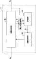
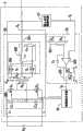
请参阅图1,其为本发明较佳实施例的中央总线电源系统的电路方框图。如图1所示,中央总线电源系统1主要包含一前级调压电路2以及至少一后级转换电路,其中前级调压电路2接收输入电压Vin,并将输入电压Vin转换为一过渡电压Vs。后级转换电路,例如图1所示的第一后级转换电路3a、第二后级转换电路3b以及第三后级转换电路3c,则与前级调压电路2电连接,其分别用以接收过渡电压Vs,并将过渡电压Vs转换为负载(未图示)所需的工作电压,以提供给负载使用,于本实施例中,第一后级转换电路3a输出第一工作电压Vo1,第二后级转换电路3b输出第二工作电压Vo2,第三后级转换电路3c输出第三工作电压Vo3。Please refer to FIG. 1 , which is a circuit block diagram of a central bus power supply system in a preferred embodiment of the present invention. As shown in Figure 1, the central bus
于一些实施例中,后级转换电路可由非隔离式的转换器所构成,更甚者,后级转换电路可由非隔离式的直流-直流转换器所构成,但并不以此为限。此外,第一工作电压Vo1可为但不限于1V,第二工作电压Vo2可为但不限于3.3V,第三工作电压Vo3可为但不限于5V。In some embodiments, the back-stage conversion circuit may be formed by a non-isolated converter, and even more, the back-stage conversion circuit may be formed by a non-isolated DC-DC converter, but not limited thereto. In addition, the first working voltage Vo1 may be but not limited to 1V, the second working voltage Vo2 may be but not limited to 3.3V, and the third working voltage Vo3 may be but not limited to 5V.
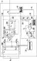
请参阅图2,其为图1所示的前级调压电路的电路方框图。如图2所示,前级调压电路2主要包含一能量转换电路20,一输入电压检测电路21、一反馈电路22以及一控制驱动电路23,其中能量转换电路20包含至少一开关元件(本图未图示),且通过开关元件的运行将输入电压Vin转换为过渡电压Vs。输入电压检测电路21与能量转换电路20电连接,用以检测与输入电压Vin相对应的一转换电压,进而输出一输入电压检测信号Vt。反馈电路22与能量转换电路20以及输入电压检测电路21电连接,用以依据输入电压检测信号Vt以及过渡电压Vs而输出一反馈控制信号Vf。至于控制驱动电路23则与能量转换电路20以及反馈电路22电连接,其接收反馈控制信号Vf,并根据反馈控制信号Vf而控制开关元件的责任周期,使能量转换电路20运行并产生过渡电压Vs。Please refer to FIG. 2 , which is a circuit block diagram of the pre-stage voltage regulating circuit shown in FIG. 1 . As shown in FIG. 2 , the pre-stage
于本实施例中,当输入电压Vin升高时,输入电压检测信号Vt对应输入电压Vin而增加,反馈控制信号Vf也对应输入电压检测信号Vt而改变,此时,控制驱动电路23便会依据反馈控制信号Vf而控制开关元件的责任周期于一责任周期预定值以上,因此本发明的前级调压电路2便可减少传导损耗、切换损耗以及滤波损耗,进而提升实际效能。In this embodiment, when the input voltage Vin rises, the input voltage detection signal Vt increases corresponding to the input voltage Vin, and the feedback control signal Vf also changes corresponding to the input voltage detection signal Vt. At this time, the
请参阅图3,并配合图2,其中图3为图2所示的前级调压电路的部分详细电路结构示意图。如图2及图3所示,能量转换电路20可为但不限于一半桥式脉冲宽度调制转换器所构成,且主要包含一第一滤波电感L1、一第一分压电路200、至少一开关元件、一变压器T以及一次级侧电路201。其中第一滤波电感L1用以对输入电流(未图示)进行滤波。第一分压电路200则与滤波电感L1电连接,用以对输入电压Vin进行分压,以提供给变压器T的初级绕组Np,且于本实施例中,第一分压电路200可为但不限于由串联连接的第一电容C1以及第二电容C2所构成。开关元件,例如图3所示的第一开关元件S1以及第二开关元件S2,则与第一分压电路200、变压器T的初级绕组Np以及控制驱动电路23电连接,第一开关元件S1以及第二开关元件S2受控制驱动电路23的控制而进行导通或截止的动作,使输入电压Vin的能量可选择性地经由第一开关元件S1以及第二开关元件S2传送至变压器T的初级绕组Np,进而使次级绕组Ns因电磁感应而产生感应交流电压Vac,且于本实施例中,第一开关元件S1及第二开关元件S2以交错的方式来进行导通或截止。Please refer to FIG. 3 together with FIG. 2 , wherein FIG. 3 is a partial detailed circuit structure diagram of the pre-stage voltage regulating circuit shown in FIG. 2 . As shown in Figures 2 and 3, the
次级侧电路201则与变压器T的次级绕组Ns电连接,用以对感应交流电压Vac进行整流及滤波,以输出过渡电压Vs,于本实施例中,次级侧电路201主要包含一同步整流电路202以及一滤波电路203,其中同步整流电路202与变压器T的次级绕组Ns电连接,用以进行同步整流,且可为但不限于由多个同步整流开关Sr所构成。滤波电路203则与同步整流电路202电连接,其用以滤波,且可为但不限于由一第一滤波电容Cf1以及一第二滤波电感L2所构成。The
当然,能量转换电路20并不局限于如图3所示由一半桥式脉冲宽度调制转换器所构成,于一些实施例中,能量转换电路20也可由例如顺向式、反驰式或是全桥式等脉冲宽度调制转换器所构成。更甚者,能量转换电路20也可由谐振式,例如串联谐振、并联谐振、LLC串联谐振或LLC并联谐振的脉冲频率调制转换器所构成。Certainly, the
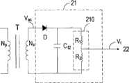
请参阅图4并配合图2及图3,其中图4为图3所示的输入电压检测电路的详细电路结构示意图。如图2至图4所示,由于本实施例中,输入电压检测电路21与变压器T的次级绕组Ns电连接,因此输入电压检测电路21所检测的转换电压实际上为次级绕组Ns上的感应交流电压Vac,而因为感应交流电压Vac的大小与输入电压Vin的大小相对应,故输入电压检测电路21通过检测感应交流电压Vac所输出的输入电压检测信号Vt也会与输入电压Vin相对应。Please refer to FIG. 4 together with FIG. 2 and FIG. 3 , wherein FIG. 4 is a detailed circuit structure diagram of the input voltage detection circuit shown in FIG. 3 . As shown in Figures 2 to 4, since in this embodiment, the input
输入电压检测电路21主要包含一整流二极管D、一第二滤波电容Cf2以及一第二分压电路210,其中整流二极管D的阳极端与变压器T的次级绕组Ns电连接,整流二极管D用以整流,第二滤波电容Cf2与整流二极管D的阴极端电连接,第二滤波电容Cf2用以滤波,第二分压电路210则与整流二极管D的阴极端、第二滤波电容Cf2以及反馈电路22电连接,且可为但不限于由一第一电阻R1以及一第二电阻R2串联连接所构成,第二分压电路210用以对经由整流二极管D整流以及经第二滤波电容Cf2滤波后的电压进行分压,以输出输入电压检测信号Vt至反馈电路22。The input
当然,输入电压检测电路21并不局限于如图3所示与变压器T的次级绕组Ns电连接,以通过检测次级绕组Ns上的感应交流电压Vac而输出输入电压检测信号Vt,于一些实施例中,输入电压检测电路21也可电连接于第一滤波电感L1的输入端、变压器T附加的初级绕组(未图示)、变压器T附加的次级绕组(未图示)、第一分压电路200中第一电容C1及第二电容C2之间的连接点或是同步整流电路202的输出侧等位置,此时输入电压检测电路21检测到的能量转换电路20的转换电压实际上便为上述这些位置所对应的电压。Of course, the input
请再参阅图3,反馈电路22主要包含一第一运算放大器220、一第三电容C3、一第三分压电路221、一光耦合器222以及一参考电压调整电路223。其中第三分压电路221与能量转换电路20的次级侧电路201以及第一运算放大器220的反向输入端电连接,其用以对次级侧电路201所输出的过渡电压Vs进行分压,以提供给第一运算放大器220的反向输入端,且于本实施例中,第三分压电路221可为但不限于由一第三电阻R3以及一第四电阻R4串联连接所构成。第三电容C3分别与第一运算放大器220的反向输入端以及输出端电连接。光耦合器222的输入端,即发光二极管元件D1与第一运算放大器220的输出端电连接,光耦合器222的输出端,即光晶体管B则与控制驱动电路23电连接。参考电压调整电路223则电连接于第一运算放大器220的非反向输入端以及输入电压检测电路21之间,用以接收输入电压检测信号Vt,并根据输入电压检测信号Vt而输出一参考电压Vref。第一运算放大器220用以比较经第三分压电路221分压后的过渡电压Vs与参考电压Vref,并依比较结果而经光耦合器222输出一反馈控制信号Vf,如此一来,控制驱动电路23便根据反馈控制信号Vf而对应地调整第一开关元件S1以及第二开关元件S2的责任周期,进而调节过渡电压Vs,也即使经第三分压电路221分压后的过渡电压Vs与参考电压Vref实质上相等。Please refer to FIG. 3 again. The
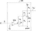
请参阅图5,并配合图2至图4,其中图5为图3所示的参考电压调整电路的详细电路结构示意图。如图2至图5所示,参考电压调整电路223主要包含一比较器2230、一电压调整开关元件S3、一可调稳压器2231、一第一电压调整电阻R5、一第二电压调整电阻R6、一第三电压调整电阻R7以及一第四电压调整电阻R8。其中第四电压调整电阻R8接收一直流电压Vcc。可调稳压器2231可为但不限于由美国国家半导体(National Semiconductor:NS)的产品编号为LM4041的积体电路所构成,且可调稳压器2231的阴极端a与第一运算放大器220的非反向输入端以及第四电压调整电阻R8电连接,可调稳压器2231的阳极端b与一接地端ground电连接,可调稳压器2231的反馈端c与第一电压调整电阻R5电连接。第三电压调整电阻R7电连接于可调稳压器2231的阴极端a及反馈端c之间,且与第一运算放大器220的非反向输入端电连接,以输出参考电压Vref。第二电压调整电阻R6电连接于可调稳压器2231的反馈端c以及阳极端b之间,因此第二电压调整电阻R6两端的电压被可调稳压器2231限定于一电压固定值,例如1.225V。第一电压调整电阻R5与电压调整开关元件S3串联连接,且第一电压调整电阻R5与电压调整开关元件S3的串联回路电连接于可调稳压器2231的反馈端c以及阳极端b之间。比较器2230的非反向输入端接收一预设电压Vad,比较器2230的反向输入端则与输入电压检测电路21电连接而接收输入电压检测信号Vt。Please refer to FIG. 5 , together with FIG. 2 to FIG. 4 , wherein FIG. 5 is a detailed circuit structure diagram of the reference voltage adjustment circuit shown in FIG. 3 . As shown in Figure 2 to Figure 5, the reference
以下将进一步说明本发明的参考电压调整电路223的动作方式以及本发明的前级调压电路2所能实现的技术效果。请参阅图6至图8,并配合图至图5,其中图6为图3所示的前级调压电路的参考电压对应于输入电压检测信号的波形图,图7为图3所示的前级调压电路的过渡电压对应于输入电压的波形图,图8为图3所示的前级调压电路的开关元件的责任周期对应于输入电压的波形图。如图所示,当输入电压Vin由0开始提升至大于一最小驱动电压Vmin以上时,中央总线电源系统1便被输入电压Vin所驱动,使得输入电压检测信号Vt由0开始提升,而当输入电压检测信号Vt尚未提升至大于预设电压Vad,即输入电压检测信号Vt小于预设电压Vad时,比较器2230便会输出一高电平的使能信号,使电压调整开关元件S3导通,进而使第一电压调整电阻R5以及第二电压调整电阻R6并联连接,因此参考电压Vref维持在如图6所示的一第一参考电平Vref1,该第一参考电平Vref1的值可例如为(R5//R6)*1.225/R7+1.225。而由图7及图8可得知,当输入电压检测信号Vt小于预设电压Vad时,过渡电压Vs维持在如图7所示的第一过渡电平Vs1,该第一过渡电平Vs1的值为{(R3+R4)/R4}*Vref1,至于能量转换电路20的开关元件,例如第一开关元件S1或第二开关元件S2的责任周期会从输入电压Vin等于最小驱动电压Vmin时开始持续的下降。The operation mode of the reference
而当输入电压Vin提升至一电压门槛值Vth,使输入电压检测信号Vt恰好大于预设电压Vad时,比较器2230便会输出一低电平的截止信号,使电压调整开关元件S3截止,此时第一电压调整电阻R5形成开路,如此一来,参考电压Vref的电平便提高至如图6所示的一第二参考电平Vref2,该第二参考电平Vref2的值可例如为(R6*1.225/R7)+1.225。而由图7及图8可得知,当输入电压检测信号Vt恰好大于预设电压Vad时,过渡电压Vs的电平提高至一第二过渡电平Vs2,该第二过渡电平Vs2的值为{(R3+R4)/R4}*Vref2,至于第一开关元件S1或第二开关元件S2的责任周期便会在一第一责任周期预定值Duty1时呈现一步阶式(step)的提升,其中该第一责任周期预定值Duty1可为但不限于60%。And when the input voltage Vin rises to a voltage threshold value Vth, so that the input voltage detection signal Vt is just greater than the preset voltage Vad, the
如图6所示,参考电压Vref随着输入电压检测信号Vt的增加而阶段地改变,因此当输入电压Vin提升至大于电压门槛值Vth而小于中央总线电源系统1所能承受的一最大驱动电压Vmax,且输入电压检测信号Vt大于预设电压Vad时,参考电压Vref的电平便会持续维持在第二参考电平Vref2,而过渡电压Vs的电平也持续维持在第二过渡电平Vs2,至于第一开关元件S1或第二开关元件S2的责任周期则会从输入电压Vin大于电压门槛值Vth时开始持续的下降,然而由图8可得知,第一开关元件S1或第二开关元件S2的责任周期在下降的过程中仍维持于在第一责任周期预定值Duty1以上。As shown in FIG. 6 , the reference voltage Vref changes step by step with the increase of the input voltage detection signal Vt. Therefore, when the input voltage Vin rises to a value greater than the voltage threshold Vth but less than a maximum driving voltage that the central
由上可知,本发明的前级调压电路2所接收的输入电压Vin由0开始提升至最小驱动电压Vmin以上时,前级调压电路2的能量转换电路20的开关元件,例如第一开关元件S1或第二开关元件S2的责任周期开始下降,然而当输入电压Vin提升至一电压门槛值Vth时,第一开关元件S1或第二开关元件S2的责任周期在第一责任周期预定值Duty1时呈现步阶式的提升,且当输入电压Vin提升至大于电压门槛值Vth而小于中央总线电源系统1所能承受的电压最大驱动电压Vmax时,第一开关元件S1或第二开关元件S2的责任周期仍维持在大于第一责任周期预定值Duty1以上,因此相较于公知前级调压电路的开关元件的责任周期随着输入电压的提升而持续地减小,本发明的前级调压电路2便可减少电能传导的损耗、第一开关元件S1或第二开关元件S2的切换损耗以及第一滤波电感L1以及滤波电路203的滤波损耗等缺陷,进而提升效能。It can be seen from the above that when the input voltage Vin received by the pre-stage
请参阅图9至图12,其中图9为图5所示的参考电压调整电路的另一变化例,图10为图9所示的参考电压调整电路应用于图3所示的前级调压电路时参考电压对应于输入电压检测信号的波形图,图11为图9所示的参考电压调整电路应用于图3所示的前级调压电路时过渡电压对应于输入电压的波形图,图12为图9所示的参考电压调整电路应用于图3所示的前级调压电路时开关元件的责任周期对应于输入电压的波形图。如图9至图12所示,本实施例的参考电压调整电路423的电路结构与图5所示的参考电压调整电路223相仿,且相同符号的元件代表结构与功能相似,故元件特征及动作方式于此不再赘述。唯相较于图5,本实施例的参考电压调整电路423并不具有如图5所示的比较器2230以及电压调整开关元件S3,此外,第一电压调整电阻R5改电连接于输入电压检测电路21以及可调稳压器2231的反馈端c之间,进而接收输入电压检测信号Vt,且第一电压调整电阻R5也与第二电压调整电阻R6以及第三电压调整电阻R7电连接,因此经可调稳压器2231所输出的参考电压Vref的值为1.225+1.225*(R5//R6)/R7+Vt*(R5//R6)/R5,由于第一电压调整电阻R5、第二电压调整电阻R6以及第三电压调整电阻R7的电阻值为常数,由此可知,此时参考电压Vref随着输入电压检测信号Vt的变化而实质上线性地改变,也即如图10及图11所示,当输入电压Vin由最小驱动电压Vmin提升至最大驱动电压Vmax而输入电压检测信号Vt持续提升时,由参考电压调整电路223所输出的参考电压Vref也对应输入电压检测信号Vt而持续地提升。Please refer to Figures 9 to 12, where Figure 9 is another variation example of the reference voltage adjustment circuit shown in Figure 5, and Figure 10 is the application of the reference voltage adjustment circuit shown in Figure 9 to the pre-stage voltage regulation shown in Figure 3 When the circuit reference voltage corresponds to the waveform diagram of the input voltage detection signal, Fig. 11 is a waveform diagram of the transition voltage corresponding to the input voltage when the reference voltage adjustment circuit shown in Fig. 9 is applied to the pre-stage voltage regulating circuit shown in Fig. 3, Fig. 12 is a waveform diagram of the duty cycle of the switching element corresponding to the input voltage when the reference voltage adjustment circuit shown in FIG. 9 is applied to the pre-stage voltage regulation circuit shown in FIG. 3 . As shown in FIGS. 9 to 12, the circuit structure of the reference voltage adjustment circuit 423 of this embodiment is similar to that of the reference
此外,当输入电压Vin由最小驱动电压Vmin提升至最大驱动电压Vmax时,过渡电压VS对应地持续提升,然而因为参考电压Vref持续地提升,且为使第三分压电路221分压后的过渡电压Vs可与参考电压Vref实质上相等,即便输入电压Vin增加,控制驱动电路23也会将第一开关元件S1或第二开关元件S2的责任周期控制在一定值而不会减少,例如图12所示大于一第二责任周期预定值Duty2以上。In addition, when the input voltage Vin increases from the minimum driving voltage Vmin to the maximum driving voltage Vmax, the transition voltage VS correspondingly continues to increase. The voltage Vs can be substantially equal to the reference voltage Vref. Even if the input voltage Vin increases, the
于其它实施例中,如图13所示,反馈电路22也可不具有如图3所示的参考电压调整电路223,此时反馈电路22的第一运算放大器220的非反向输入端则对应地改与输入电压检测电路21电连接而接收输入电压检测信号Vt,如此一来,反馈电路22的第一运算放大器220的非反向输入端所接收的参考电压则直接为输入电压检测信号Vt,因此当输入电压Vin提升时,输入电压检测信号Vt也跟着提升,而为了使第三分压电路221分压后的过渡电压Vs与输入电压检测信号Vt实质上相等,过渡电压Vs便持续的增加,故即便输入电压Vin增加,控制驱动电路23也会控制第一开关元件S1或第二开关元件S2的责任周期维持在一定值而不会减少,以具有如图12所示的相似效果,换言之,即第一开关元件S1或第二开关元件S2的责任周期也会大于一第三责任周期预定值以上(未图示)。In other embodiments, as shown in FIG. 13 , the
于一些实施例中,控制驱动电路23可为脉冲宽度调制控制驱动电路所构成,但不以此为限,当能量转换电路20为谐振式的脉冲频率调制转换器所构成时,控制驱动电路23也可为脉冲频率调制控制驱动电路所构成。In some embodiments, the
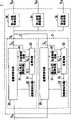
当然,中央总线电源系统1并不局限于如图1所示仅具有一前级调压电路2,于一些实施例中,如图14所示,中央总线电源系统1也可具有多个前级调压电路2,这些前级调压电路2相互并联连接以构成一并联式调压电路系统,因此中央总线电源系统1便可通过并联连接的多个前级调压电路2而提供较大的输出功率给后级转换电路。Certainly, the central bus
此外,为了使多个前级调压电路2具有电流分配技术(current sharing technique),即每一前级调压电路2的输出电流Io可与其它的前级调压电路2实现匹配,例如均流,以平均分配提供给后级转换电路所需的电流,如图14所示,每一前级调压电路2更可为但不限于包含一电流检测电路24,其与能量转换电路20以及反馈电路22电连接,用以检测能量转换电路20内与输出电流Io相对应的一转换电流,以输出一电流检测信号Vfc至反馈电路22,使反馈电路22更对应电流检测信号Vfc、输入电压检测信号Vt以及过渡电压Vs改变反馈控制信号Vf,如此一来,控制驱动电路23便调整例如第一开关元件S1或第二开关元件S2的责任周期来改变前级调压电路2的过渡电压Vs,因此除了过渡电压Vs会随着输入电压Vin的改变而调整,前级调压电路2的输出电流Io与其它的前级调压电路2的输出电流Io也可实现匹配,举例而言,当多个前级调压电路2的其中之一前级调压电路2的输出电流Io过大时,电流检测电路24便会输出代表输出电流Io过大的电流检测信号Vfc给反馈电路22,使反馈电路22对应输入电压检测信号Vt及电流检测信号Vfc而输出相对应的反馈控制信号Vf,如此一来,控制驱动电路23便会根据反馈控制信号Vf调整第一开关元件S1或第二开关元件S2的责任周期,使过渡电压Vs下降,进而降低输出电流Io,以使其与其它的前级调压电路2负担相同的负载电流。In addition, in order to make a plurality of pre-stage voltage regulating circuits 2 have a current sharing technique (current sharing technique), that is, the output current Io of each pre-stage voltage regulating circuit 2 can be matched with other pre-stage voltage regulating circuits 2, for example, equal flow, to evenly distribute the current required by the subsequent stage conversion circuit, as shown in Figure 14, each pre-stage voltage regulation circuit 2 may further include but not limited to a current detection circuit 24, which is connected with the energy conversion circuit 20 and The feedback circuit 22 is electrically connected to detect a conversion current corresponding to the output current Io in the energy conversion circuit 20, so as to output a current detection signal Vfc to the feedback circuit 22, so that the feedback circuit 22 is more corresponding to the current detection signal Vfc and the input voltage The detection signal Vt and the transition voltage Vs change the feedback control signal Vf, so that the control drive circuit 23 adjusts, for example, the duty cycle of the first switching element S1 or the second switching element S2 to change the transition voltage Vs of the pre-stage voltage regulating circuit 2 , so in addition to the transition voltage Vs will be adjusted with the change of the input voltage Vin, the output current Io of the pre-stage voltage regulation circuit 2 can also be matched with the output current Io of other pre-stage voltage regulation circuits 2, for example, when When the output current Io of one of the pre-stage voltage regulating circuits 2 is too large, the current detection circuit 24 will output a current detection signal Vfc representing the excessive output current Io to the feedback circuit 22, so that The feedback circuit 22 outputs a corresponding feedback control signal Vf corresponding to the input voltage detection signal Vt and the current detection signal Vfc, so that the control drive circuit 23 adjusts the first switching element S1 or the second switching element according to the feedback control signal Vf The duty cycle of S2 reduces the transition voltage Vs, thereby reducing the output current Io, so that it bears the same load current as other pre-stage voltage regulating circuits 2 .
请参阅图15,其为图14所示的前级调压电路的部分详细电路结构示意图。如图15所示,电流检测电路24主要包含一感测元件241、一信号放大器242、一第一放大比例调整电阻R9以及一第二放大比例调整电阻R10,其中感测元件241可由电阻所构成,但不以此为限,感测元件241也可由其他电流感测元件,例如电流变压器、霍尔电流传感器(Hall-Effect Current Sensor)或是同步整流开关Sr的导通电阻等来构成,感测元件241与次级测电路201的输出端电连接,其用以检测与输出电流Io相对应的一转换电流,于本实施例中,转换电流实际上为输出电流Io,此外,感测元件241更会对应转换电流而输出一电流感测信号Vc。信号放大器242、第一放大比例调整电阻R9以及一第二放大比例调整电阻R10则构成一信号放大电路,该信号放大电路与感测元件241以及第四电阻R4电连接,用以调整电流感测信号Vc,例如本实施例中,将电流感测信号Vc放大R10/R9倍,以产生一电流检测信号Vfc,并通过第四电阻R4传送至第一运算放大器220的反向输入端,使第一运算放大器220对应电流检测信号Vfc、经第三分压电路221分压后的过渡电压Vs以及输入电压检测信号Vt而产生反馈控制信号Vf,使控制驱动电路23控制第一开关元件S1或第二开关元件S2的责任周期来调整过渡电压Vs,进而使前级调压电路2的输出电流Io可与其它前级调压电路2的输出电流Io实现匹配。Please refer to FIG. 15 , which is a partial detailed circuit structure diagram of the pre-stage voltage regulating circuit shown in FIG. 14 . As shown in FIG. 15 , the
当然,感测元件241所检测的转换电流实际上并不局限于如上所述为输出电流Io,可依感测元件241连接位置的不同而有不同的实施方式,因此只要感测元件241连接的位置所检测到的转换电流与输出电流Io有对应关,都在本发明的保护范围内。Of course, the switching current detected by the
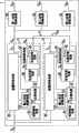
请参阅图16,其为图14所示的中央总线电源系统的一变化例。如图16所示,本实施例的中央总线电源系统1的电路结构与图14所示的中央总线电源系统1相仿,且相同符号的元件代表结构与功能相似,故元件特征及动作方式于此不再赘述。Please refer to FIG. 16 , which is a modified example of the central bus power system shown in FIG. 14 . As shown in FIG. 16, the circuit structure of the central bus
唯相较于图14所示的中央总线电源系统1,本实施例的中央总线电源系统1的每一前级调压电路2更具有一电流共享电路25、一电流匹配电路26以及电流共享总线4,此外,电流检测电路24与能量转换电路20、电流共享电路25以及电流匹配电路26电连接。Only compared with the central bus
电流共享电路25与电流检测电路24电连接,并经由电流共享总线4而与其它前级调压电路2的电流共享电路25电连接,电流共享电路25接收由电流检测电路24所输出的电流检测信号Vfc,此外,电流共享电路25也传送一电流共享信号Vcs至电流共享总线4,其中该电流共享总线信号Vcs代表着中央总线电源系统1内的多个前级调压电路2的输出电流Io的平均值或是多个前级调压电路2的输出电流Io中的最大电流值。电流匹配电路26则与电流检测电路24、电流共享总线4以及反馈电路22电连接,用以对电流检测信号Vfc与电流共享总线信号Vcs的差异进行处理,使反馈电路22可依据电流检测信号Vfc与电流共享总线信号Vcs两者间的差异而对应地调整反馈控制信号Vf,因此控制驱动电路23便依据反馈控制信号Vf调整第一开关元件S1或第二开关元件S2的责任周期,以改变前级调压电路2的输出电流Io,故除了过渡电压Vs会随着输入电压Vin的改变而调整,电流检测信号Vfc也会被调整于等于电流共享总线信号Vcs,如此一来,前级调压电路2的输出电流Io与其它前级调压电路2的输出电流Io便可实现匹配。The
请参阅图17,其为图16所示的前级调压电路的部分详细电路结构示意图。如图17所示,每一前级调压电路2的电流共享电路25主要包含一第二运算放大器250以及一第一逆向电流阻隔二极管D2,其中第二运算放大器260的非反向输入端与电流检测电路24电连接而接收电流检测信号Vfc,第二运算放大器250的反向输入端则经由电流共享总线4与其它前级调压电路2的电流共享电路25电连接,第二运算放大器250的输出端与第一逆向电流阻隔二极管D2的阳极端电连接,因此第二运算放大器250便可将非反向输入端所接收的电流检测信号Vfc与其它前级调压电路2的电流共享电路25所接收的电流检测信号进行沟通,进而经由第一逆向电流阻隔二极管D2输出电流共享总线信号Vcs。Please refer to FIG. 17 , which is a partial detailed circuit structure diagram of the pre-stage voltage regulating circuit shown in FIG. 16 . As shown in FIG. 17 , the
电流匹配电路26包含一第二逆向电流阻隔二极管D3、第三运算放大器260、第五电阻R11以及第四电容C4,其中第三运算放大器260的反向输出端经由第五电阻R11而与第一逆向电流阻隔二极管D2的阴极端电连接,以接收电流共享总线信号Vcs,第三运算放大器260的非反向输入端与电流检测电路24电连接而接收电流检测信号Vfc,第三运算放大器260的输出端与第二逆向电流阻隔二极管D3的阴极端电连接,第二逆向电流阻隔二极管D3的阳极端与第一运算放大器220的反向输入端电连接。第三运算放大器260与第五电阻R11以及第四电容C4构成一比例积分器,故比例积分器与电流共享总线4以及电流检测电路24电连接,比例积分器对电流检测信号Vfc与电流共享总线信号Vcs的差异进行处理,并将处理的结果经由第二逆向电流阻隔二极管D3传送至反馈电路22,故反馈电路22便依据电流检测信号Vfc与电流共享总线信号Vcs两者间的差异而对应地调整反馈控制信号Vf,因此控制驱动电路23便依据反馈控制信号Vf调整第一开关元件S1或第二开关元件S2的责任周期,以改变前级调压电路2的输出电流Io,使电流检测信号Vfc与电流共享总线信号Vcs实质上相等,如此一来,前级调压电路2的输出电流Io与其它前级调压电路2的输出电流Io便可实现匹配。The
综上所述,本发明提供一种调压电路及其适用的并联式调压电路系统,其包括一能量转换电路,一输入电压检测电路,一反馈电路以及控制驱动电路。该输入电压检测电路检测能量转换电路内与输入电压相对应的一转换电压,使反馈电路可依据转换电压及能量转换电路所输出的过渡电压而输出反馈控制信号,如此一来,控制驱动电路便可根据反馈控制信号而调整开关元件的责任周期,使开关元件的责任周期在输入电压提升的过程中,可保持于一责任周期预定值以上,进而使前级调压电路的传导损耗、开关元件的切换损耗以及滤波电感或滤波电路的滤波损耗降低并提升效能。To sum up, the present invention provides a voltage regulation circuit and its applicable parallel voltage regulation circuit system, which includes an energy conversion circuit, an input voltage detection circuit, a feedback circuit and a control drive circuit. The input voltage detection circuit detects a conversion voltage corresponding to the input voltage in the energy conversion circuit, so that the feedback circuit can output a feedback control signal according to the conversion voltage and the transition voltage output by the energy conversion circuit. In this way, the control drive circuit can be easily The duty cycle of the switching element can be adjusted according to the feedback control signal, so that the duty cycle of the switching element can be kept above a predetermined duty cycle during the process of increasing the input voltage, thereby reducing the conduction loss of the pre-stage voltage regulating circuit and the switching element The switching loss of the filter and the filter loss of the filter inductor or the filter circuit are reduced and the performance is improved.
本发明得由本领域技术人员任施匠思而为诸般修饰,都不脱如附权利要求所欲保护的范围。The present invention can be modified in various ways by those skilled in the art without departing from the protection scope of the appended claims.
Claims (42)
Translated fromChineseApplications Claiming Priority (2)
| Application Number | Priority Date | Filing Date | Title |
|---|---|---|---|
| US22937609P | 2009-07-29 | 2009-07-29 | |
| US61/229,376 | 2009-07-29 |
Publications (2)
| Publication Number | Publication Date |
|---|---|
| CN101989814Atrue CN101989814A (en) | 2011-03-23 |
| CN101989814B CN101989814B (en) | 2013-10-09 |
Family
ID=43526833
Family Applications (1)
| Application Number | Title | Priority Date | Filing Date |
|---|---|---|---|
| CN2010102414249AActiveCN101989814B (en) | 2009-07-29 | 2010-07-29 | Voltage Regulating Circuit and Its Applicable Parallel Voltage Regulating Circuit System |
Country Status (3)
| Country | Link |
|---|---|
| US (1) | US8787040B2 (en) |
| CN (1) | CN101989814B (en) |
| TW (1) | TWI401555B (en) |
Cited By (10)
| Publication number | Priority date | Publication date | Assignee | Title |
|---|---|---|---|---|
| CN102761247A (en)* | 2011-04-26 | 2012-10-31 | 登丰微电子股份有限公司 | Control circuit of conversion circuit |
| CN104679085A (en)* | 2013-11-30 | 2015-06-03 | 鸿富锦精密工业(深圳)有限公司 | Power supply regulating device |
| WO2015120689A1 (en)* | 2014-02-17 | 2015-08-20 | 华为技术有限公司 | Dc-to-dc conversion circuit and method |
| CN105048815A (en)* | 2015-05-05 | 2015-11-11 | 北京新雷能科技股份有限公司 | Output voltage regulating circuit and power supply |
| US9337741B2 (en) | 2014-02-17 | 2016-05-10 | Huawei Technologies Co., Ltd. | DC-DC conversion circuit and method |
| CN104396132B (en)* | 2012-08-27 | 2017-05-10 | 富士电机株式会社 | Switching power supply device |
| CN104067498B (en)* | 2012-01-30 | 2018-02-27 | 瑞典爱立信有限公司 | Controlling Switch Mode Power Supplies to Maximize Power Efficiency |
| CN108011499A (en)* | 2014-01-10 | 2018-05-08 | 雅达电子国际有限公司 | Control circuit and method for adjusting output voltage using multiple and/or adjustable reference voltages |
| CN108631579A (en)* | 2018-06-12 | 2018-10-09 | 漳州科华技术有限责任公司 | A kind of UPS and its DC bus-bar voltage method of adjustment, system, equipment |
| US11223289B2 (en) | 2020-01-17 | 2022-01-11 | Astec International Limited | Regulated switched mode power supplies having adjustable output voltages |
Families Citing this family (32)
| Publication number | Priority date | Publication date | Assignee | Title |
|---|---|---|---|---|
| CN103683944B (en)* | 2012-09-21 | 2016-09-14 | 台达电子工业股份有限公司 | Voltage supply system, converter therein, and voltage adjustment method |
| US10153701B2 (en)* | 2011-03-03 | 2018-12-11 | Telefonaktiebolaget Lm Ericsson (Publ) | Controlling a switched mode power supply with maximised power efficiency |
| EP2700137B1 (en)* | 2011-04-20 | 2017-06-07 | Telefonaktiebolaget LM Ericsson (publ) | Control of dynamic bus voltage in an intermediate bus architecture power system |
| US10680515B2 (en) | 2011-05-05 | 2020-06-09 | Psemi Corporation | Power converters with modular stages |
| EP4318909A3 (en) | 2011-05-05 | 2024-03-06 | PSEMI Corporation | Dc-dc converter with modular stages |
| US20120297104A1 (en)* | 2011-05-20 | 2012-11-22 | General Electric | Controlled intermediate bus architecture optimization |
| US8743553B2 (en) | 2011-10-18 | 2014-06-03 | Arctic Sand Technologies, Inc. | Power converters with integrated capacitors |
| WO2013059961A1 (en)* | 2011-10-27 | 2013-05-02 | Telefonaktiebolaget L M Ericsson (Publ) | Fully-regulated power converter |
| TWI457548B (en)* | 2011-12-16 | 2014-10-21 | Au Optronics Corp | Light sense appratus and method of adjustion thereof |
| US8723491B2 (en) | 2011-12-19 | 2014-05-13 | Arctic Sand Technologies, Inc. | Control of power converters with capacitive energy transfer |
| US9158314B2 (en) | 2013-01-09 | 2015-10-13 | Richtek Technology Corporation | Voltage regulator, and control circuit and control method thereof |
| US8724353B1 (en) | 2013-03-15 | 2014-05-13 | Arctic Sand Technologies, Inc. | Efficient gate drivers for switched capacitor converters |
| US8619445B1 (en) | 2013-03-15 | 2013-12-31 | Arctic Sand Technologies, Inc. | Protection of switched capacitor power converter |
| US9407154B2 (en) | 2013-06-14 | 2016-08-02 | Advanced Charging Technologies, LLC | Electrical circuit for delivering power to consumer electronic devices |
| US10141844B2 (en)* | 2013-07-16 | 2018-11-27 | Lion Semiconductor Inc. | Reconfigurable power regulator |
| US10693368B2 (en) | 2014-03-14 | 2020-06-23 | Psemi Corporation | Charge pump stability control |
| DE112015001245T5 (en) | 2014-03-14 | 2016-12-15 | Arctic Sand Technologies, Inc. | Charge-balanced charge pump control |
| DE112015001260T5 (en) | 2014-03-14 | 2016-12-08 | Arctic Sand Technologies, Inc. | Charge pump stability control |
| CN104079176B (en)* | 2014-06-20 | 2016-11-23 | 华为技术有限公司 | A kind of method for managing power supply and power supply |
| DE102014211854A1 (en)* | 2014-06-20 | 2015-12-24 | Robert Bosch Gmbh | Device and method for determining an electrical voltage |
| WO2016149063A1 (en) | 2015-03-13 | 2016-09-22 | Arctic Sand Technologies, Inc. | Dc-dc transformer with inductor for the facilitation of adiabatic inter-capacitor charge transport |
| WO2017007991A1 (en) | 2015-07-08 | 2017-01-12 | Arctic Sand Technologies, Inc. | Switched-capacitor power converters |
| WO2017007387A1 (en)* | 2015-07-09 | 2017-01-12 | Telefonaktiebolaget Lm Ericsson (Publ) | Isolated buck converter, switched mode power supply, and method of transferring digital data from a primary side to an isolated secondary side of an isolated buck converter |
| EP3282550B1 (en) | 2016-02-05 | 2020-04-15 | Guangdong Oppo Mobile Telecommunications Corp., Ltd. | Adapter and charging control method |
| US9729073B1 (en)* | 2016-02-05 | 2017-08-08 | Power Forest Technology Corporation | Power conversion apparatus |
| JP6843696B2 (en) | 2017-04-28 | 2021-03-17 | キヤノン株式会社 | Power supply device and image forming device |
| TWI666861B (en)* | 2017-09-01 | 2019-07-21 | 明緯(廣州)電子有限公司 | Control circuit for reducing power loss of llc resonant converter during light-load or no-load operation |
| US10686367B1 (en) | 2019-03-04 | 2020-06-16 | Psemi Corporation | Apparatus and method for efficient shutdown of adiabatic charge pumps |
| TWI729835B (en) | 2020-06-03 | 2021-06-01 | 亞源科技股份有限公司 | Hysteresis voltage detection circuit |
| TWI759932B (en)* | 2020-11-02 | 2022-04-01 | 國立臺灣科技大學 | Interleaved three phase wye-delta connected power converter |
| US11682962B2 (en)* | 2021-04-27 | 2023-06-20 | Infineon Technologies Ag | Circuit for controlling an output of a power converter |
| CN113783262A (en)* | 2021-09-15 | 2021-12-10 | 淮海机电科技股份有限公司 | Charger power feedback regulation and control circuit |
Citations (8)
| Publication number | Priority date | Publication date | Assignee | Title |
|---|---|---|---|---|
| JPH09233816A (en)* | 1996-02-22 | 1997-09-05 | Matsushita Electric Ind Co Ltd | Switching power supply |
| JPH11187662A (en)* | 1997-12-24 | 1999-07-09 | Isuzu Motors Ltd | Dc-to-dc converter |
| CN1246986A (en)* | 1997-02-06 | 2000-03-08 | 太平洋水泥株式会社 | Control circuit and control method of piezoelectric transformer |
| JP2000139079A (en)* | 1998-05-29 | 2000-05-16 | Fairchild Korea Semiconductor Ltd | Power factor collection controller |
| CN1295374A (en)* | 1999-09-01 | 2001-05-16 | 英特赛尔公司 | Multi-phase converter with balanced current |
| US20050286271A1 (en)* | 2002-01-31 | 2005-12-29 | Vlt Corporation, A California Corporation | Point of load sine amplitude converters and methods |
| US20080247194A1 (en)* | 2007-04-03 | 2008-10-09 | Delta Electronics, Inc. | Resonant converter system and controlling method thereof having relatively better efficiency |
| US20080266907A1 (en)* | 2007-04-25 | 2008-10-30 | Jin-Tae Kim | Switch controller, switch control method, converter using the same, and driving method thereof |
Family Cites Families (5)
| Publication number | Priority date | Publication date | Assignee | Title |
|---|---|---|---|---|
| US6944034B1 (en)* | 2003-06-30 | 2005-09-13 | Iwatt Inc. | System and method for input current shaping in a power converter |
| JP4468011B2 (en)* | 2004-02-25 | 2010-05-26 | キヤノン株式会社 | Switching power supply and image forming apparatus |
| US7280376B2 (en)* | 2004-10-15 | 2007-10-09 | Dell Products L.P. | Primary side voltage sense for AC/DC power supplies capable of compensation for a voltage drop in the secondary |
| JP4908386B2 (en)* | 2007-11-30 | 2012-04-04 | コーセル株式会社 | Switching power supply device and driving method thereof |
| US8098506B2 (en)* | 2009-06-02 | 2012-01-17 | Power Integrations, Inc. | Single-stage power supply with power factor correction and constant current output |
- 2010
- 2010-07-29TWTW099125001Apatent/TWI401555B/enactive
- 2010-07-29USUS12/845,898patent/US8787040B2/enactiveActive
- 2010-07-29CNCN2010102414249Apatent/CN101989814B/enactiveActive
Patent Citations (8)
| Publication number | Priority date | Publication date | Assignee | Title |
|---|---|---|---|---|
| JPH09233816A (en)* | 1996-02-22 | 1997-09-05 | Matsushita Electric Ind Co Ltd | Switching power supply |
| CN1246986A (en)* | 1997-02-06 | 2000-03-08 | 太平洋水泥株式会社 | Control circuit and control method of piezoelectric transformer |
| JPH11187662A (en)* | 1997-12-24 | 1999-07-09 | Isuzu Motors Ltd | Dc-to-dc converter |
| JP2000139079A (en)* | 1998-05-29 | 2000-05-16 | Fairchild Korea Semiconductor Ltd | Power factor collection controller |
| CN1295374A (en)* | 1999-09-01 | 2001-05-16 | 英特赛尔公司 | Multi-phase converter with balanced current |
| US20050286271A1 (en)* | 2002-01-31 | 2005-12-29 | Vlt Corporation, A California Corporation | Point of load sine amplitude converters and methods |
| US20080247194A1 (en)* | 2007-04-03 | 2008-10-09 | Delta Electronics, Inc. | Resonant converter system and controlling method thereof having relatively better efficiency |
| US20080266907A1 (en)* | 2007-04-25 | 2008-10-30 | Jin-Tae Kim | Switch controller, switch control method, converter using the same, and driving method thereof |
Cited By (14)
| Publication number | Priority date | Publication date | Assignee | Title |
|---|---|---|---|---|
| CN102761247A (en)* | 2011-04-26 | 2012-10-31 | 登丰微电子股份有限公司 | Control circuit of conversion circuit |
| CN104067498B (en)* | 2012-01-30 | 2018-02-27 | 瑞典爱立信有限公司 | Controlling Switch Mode Power Supplies to Maximize Power Efficiency |
| CN104396132B (en)* | 2012-08-27 | 2017-05-10 | 富士电机株式会社 | Switching power supply device |
| US9787204B2 (en) | 2012-08-27 | 2017-10-10 | Fuji Electric Co., Ltd. | Switching power supply device |
| CN104679085B (en)* | 2013-11-30 | 2017-02-15 | 上海德朗能新能源有限公司 | Power supply regulating device |
| CN104679085A (en)* | 2013-11-30 | 2015-06-03 | 鸿富锦精密工业(深圳)有限公司 | Power supply regulating device |
| CN108011499A (en)* | 2014-01-10 | 2018-05-08 | 雅达电子国际有限公司 | Control circuit and method for adjusting output voltage using multiple and/or adjustable reference voltages |
| CN108011499B (en)* | 2014-01-10 | 2020-05-12 | 雅达电子国际有限公司 | Control circuit and method for adjusting output voltage using multiple and/or adjustable reference voltages |
| US9337741B2 (en) | 2014-02-17 | 2016-05-10 | Huawei Technologies Co., Ltd. | DC-DC conversion circuit and method |
| WO2015120689A1 (en)* | 2014-02-17 | 2015-08-20 | 华为技术有限公司 | Dc-to-dc conversion circuit and method |
| CN105048815A (en)* | 2015-05-05 | 2015-11-11 | 北京新雷能科技股份有限公司 | Output voltage regulating circuit and power supply |
| CN105048815B (en)* | 2015-05-05 | 2017-11-24 | 北京新雷能科技股份有限公司 | A kind of output voltage regulation circuit and power supply |
| CN108631579A (en)* | 2018-06-12 | 2018-10-09 | 漳州科华技术有限责任公司 | A kind of UPS and its DC bus-bar voltage method of adjustment, system, equipment |
| US11223289B2 (en) | 2020-01-17 | 2022-01-11 | Astec International Limited | Regulated switched mode power supplies having adjustable output voltages |
Also Published As
| Publication number | Publication date |
|---|---|
| US20110026275A1 (en) | 2011-02-03 |
| CN101989814B (en) | 2013-10-09 |
| TW201120606A (en) | 2011-06-16 |
| US8787040B2 (en) | 2014-07-22 |
| TWI401555B (en) | 2013-07-11 |
Similar Documents
| Publication | Publication Date | Title |
|---|---|---|
| CN101989814B (en) | Voltage Regulating Circuit and Its Applicable Parallel Voltage Regulating Circuit System | |
| US10581332B2 (en) | Dimmer and power converter | |
| TWI396366B (en) | Controllers, circuits and methods for driving a load and the electronic systems thereof | |
| US9077262B2 (en) | Cascaded switching power converter for coupling a photovoltaic energy source to power mains | |
| US8749212B2 (en) | Method and apparatus to control a power factor correction circuit | |
| US9081401B2 (en) | Switching regulator and control circuit and control method thereof | |
| US10673331B2 (en) | Circuit with reduced light load power dissipation and a method thereof | |
| TWI442677B (en) | Power supply and controller thereof | |
| US9491819B2 (en) | Hysteretic power factor control method for single stage power converters | |
| US8378584B2 (en) | Power factor converter and method | |
| TWI499183B (en) | Power factor correction circuit of power converter | |
| CN110460230B (en) | Power factor correction controller, offline converter and method thereof | |
| CN101110551A (en) | Synchronous voltage modulation circuit for resonant power supply conversion circuit | |
| JP6895502B2 (en) | Dimming circuit and dimming control method | |
| KR20080004704A (en) | Power Factor Correction Circuit for Single Power Operation in BCM Mode | |
| CN104272572B (en) | Switching power supply circuit and LED lighting device | |
| CN103781257A (en) | System and method for adjusting current of light-emitting diode | |
| CN101834527B (en) | Two-stage switching power conversion circuit | |
| TW201334380A (en) | Power supply circuit, switching regulator, and control circuit and control method thereof | |
| CN103533710B (en) | A kind of LED driver | |
| CN102263507A (en) | Switch type power supply and control method applied therein | |
| CN103997220A (en) | Switching power source device and control IC which are capable of performing constant power control | |
| US7312597B2 (en) | Actuation circuit for a switch in a switch-mode converter for improving the response to sudden changes | |
| CN104702092B (en) | Power Factor Correction Circuits for Power Converters | |
| KR101022613B1 (en) | Integrated circuits for AC power supplies and AC power supplies |
Legal Events
| Date | Code | Title | Description |
|---|---|---|---|
| C06 | Publication | ||
| PB01 | Publication | ||
| C10 | Entry into substantive examination | ||
| SE01 | Entry into force of request for substantive examination | ||
| C14 | Grant of patent or utility model | ||
| GR01 | Patent grant |