CN101989136B - Touch screen and display device - Google Patents
Touch screen and display deviceDownload PDFInfo
- Publication number
- CN101989136B CN101989136BCN2009101095690ACN200910109569ACN101989136BCN 101989136 BCN101989136 BCN 101989136BCN 2009101095690 ACN2009101095690 ACN 2009101095690ACN 200910109569 ACN200910109569 ACN 200910109569ACN 101989136 BCN101989136 BCN 101989136B
- Authority
- CN
- China
- Prior art keywords
- transparency conducting
- conducting layer
- layer
- matrix
- touch
- Prior art date
- Legal status (The legal status is an assumption and is not a legal conclusion. Google has not performed a legal analysis and makes no representation as to the accuracy of the status listed.)
- Active
Links
Images


Classifications
- G—PHYSICS
- G06—COMPUTING OR CALCULATING; COUNTING
- G06F—ELECTRIC DIGITAL DATA PROCESSING
- G06F3/00—Input arrangements for transferring data to be processed into a form capable of being handled by the computer; Output arrangements for transferring data from processing unit to output unit, e.g. interface arrangements
- G06F3/01—Input arrangements or combined input and output arrangements for interaction between user and computer
- G06F3/03—Arrangements for converting the position or the displacement of a member into a coded form
- G06F3/041—Digitisers, e.g. for touch screens or touch pads, characterised by the transducing means
- G06F3/045—Digitisers, e.g. for touch screens or touch pads, characterised by the transducing means using resistive elements, e.g. a single continuous surface or two parallel surfaces put in contact
Landscapes
- Engineering & Computer Science (AREA)
- General Engineering & Computer Science (AREA)
- Theoretical Computer Science (AREA)
- Human Computer Interaction (AREA)
- Physics & Mathematics (AREA)
- General Physics & Mathematics (AREA)
- Position Input By Displaying (AREA)
- Devices For Indicating Variable Information By Combining Individual Elements (AREA)
Abstract
Translated fromChinese
Description
Translated fromChinese技术领域technical field
本发明涉及一种触摸屏及显示装置,尤其涉及一种采用碳纳米管的触摸屏及使用该触摸屏的显示装置。The invention relates to a touch screen and a display device, in particular to a touch screen using carbon nanotubes and a display device using the touch screen.
背景技术Background technique
近年来,伴随着移动电话与触摸导航系统等各种电子设备的高性能化和多样化的发展,在液晶等显示设备的前面安装透光性的触摸屏的电子设备逐步增加。这样的电子设备的利用者通过触摸屏,一边对位于触摸屏背面的显示设备的显示内容进行视觉确认,一边利用手指或笔等按压触摸屏来进行操作。由此,可以操作电子设备的各种功能。In recent years, along with the high performance and diversification of various electronic devices such as mobile phones and touch navigation systems, the number of electronic devices in which a light-transmitting touch panel is mounted on the front of a display device such as a liquid crystal is increasing. A user of such an electronic device performs operations by pressing the touch panel with a finger, a pen, or the like while visually confirming display contents of a display device located on the back of the touch panel through the touch panel. Thereby, various functions of the electronic device can be operated.
按照触摸屏的工作原理和传输介质的不同,现有的触摸屏分为四种类型,分别为电阻式、电容式、红外线式以及表面声波式。其中电阻式触摸屏及电容式触摸屏的应用比较广泛(K.Noda,K.Tanimura,Electronics andCommunications in Japan,Part 2,Vol.84,No.7,P40(2001);李树本,王清弟,吉建华,光电子技术,Vol.15,P62(1995))。According to different working principles and transmission media of touch screens, existing touch screens are divided into four types, namely resistive type, capacitive type, infrared type and surface acoustic wave type. Among them, resistive touch screen and capacitive touch screen are widely used (K.Noda, K.Tanimura, Electronics and Communications in Japan, Part 2, Vol.84, No.7, P40 (2001); Li Shuben, Wang Qingdi, Ji Jianhua, Optoelectronics Technology, Vol.15, P62(1995)).
现有的电阻式触摸屏一般包括一第一基板,该第一基板的第一表面形成有一第一透明导电层;一第二基板,该第二基板的第二表面形成有一第二透明导电层;该第一透明导电层与该第二透明导电层相对设置;以及多个点状隔离物(Dot Spacer),该多个点状隔离物设置在第一透明导电层与第二透明导电层之间。其中,所述第一透明导电层与第二透明导电层通常采用具有导电特性的铟锡氧化物(Indium Tin Oxide,ITO)层(下称ITO层)。当使用手指或笔按压第一基板时,第一基板发生扭曲,使得按压处的第一透明导电层与第二透明导电层彼此接触。通过外接的电子电路分别向第一透明导电层与第二透明导电层依次施加电压,电子电路能够检测出被按压的位置。进一步地,电子电路可根据检测的被按压位置启动电子设备的各种功能切换。The existing resistive touch screen generally includes a first substrate, a first transparent conductive layer is formed on the first surface of the first substrate; a second substrate, a second transparent conductive layer is formed on the second surface of the second substrate; The first transparent conductive layer is arranged opposite to the second transparent conductive layer; and a plurality of dot spacers (Dot Spacers), the plurality of dot spacers are arranged between the first transparent conductive layer and the second transparent conductive layer . Wherein, the first transparent conductive layer and the second transparent conductive layer usually use an indium tin oxide (Indium Tin Oxide, ITO) layer (hereinafter referred to as an ITO layer) with conductive properties. When the first substrate is pressed with a finger or a pen, the first substrate is twisted, so that the first transparent conductive layer and the second transparent conductive layer at the pressed place are in contact with each other. Through the external electronic circuit respectively applying voltages to the first transparent conductive layer and the second transparent conductive layer sequentially, the electronic circuit can detect the pressed position. Further, the electronic circuit can start various function switching of the electronic device according to the detected pressed position.
现有技术中的电容型触摸屏包括一玻璃基板,以及一透明导电层。在该电容型触摸屏中,透明导电层为例如铟锡氧化物(ITO)或锑锡氧化物(ATO)等透明材料。当手指等触摸物触摸在触摸屏表面上时,由于人体电场,手指等触摸物和触摸屏中的透明导电层之间形成一个耦合电容。对于高频电流来说,电容是直接导体,手指等触摸物的触摸将从接触点吸走一个很小的电流。触摸屏控制器通过对这个电流进行精确的计算,得出触摸点的位置。A capacitive touch screen in the prior art includes a glass substrate and a transparent conductive layer. In the capacitive touch screen, the transparent conductive layer is a transparent material such as indium tin oxide (ITO) or antimony tin oxide (ATO). When a touch object such as a finger touches the surface of the touch screen, due to the electric field of the human body, a coupling capacitance is formed between the touch object such as the finger and the transparent conductive layer in the touch screen. For high-frequency currents, capacitance is a direct conductor, and the touch of a finger or other touching object will draw a small current from the contact point. The touch screen controller obtains the position of the touch point through precise calculation of this current.
因此,提高透明导电层的导电性能,将有利于提高触摸屏的精确度及灵敏度。Therefore, improving the conductive performance of the transparent conductive layer will help to improve the accuracy and sensitivity of the touch screen.
发明内容Contents of the invention
有鉴于此,确有必要提供一种精确度高、灵敏度高及柔韧性好的触摸屏,以及使用该触摸屏的显示装置。In view of this, it is necessary to provide a touch screen with high precision, high sensitivity and good flexibility, and a display device using the touch screen.
一种触摸屏,包括:一第一电极板,该第一电极板包括一第一基体及一第一透明导电层,该第一基体具有一第一表面,该第一透明导电层设置在该第一基体的第一表面;以及一第二电极板,该第二电极板与第一电极板间隔设置,该第二电极板包括一第二基体及一第二透明导电层,该第二基体具有一第二表面,所述第二透明导电层设置在该第二基体的第二表面,该第二透明导电层与所述第一透明导电层相对设置;其中,所述第一透明导电层与第二透明导电层中至少一个透明导电层包括一碳纳米管金属复合层。A touch screen, comprising: a first electrode plate, the first electrode plate includes a first substrate and a first transparent conductive layer, the first substrate has a first surface, the first transparent conductive layer is arranged on the first A first surface of a base body; and a second electrode plate, the second electrode plate is spaced from the first electrode plate, the second electrode plate includes a second base body and a second transparent conductive layer, the second base body has A second surface, the second transparent conductive layer is arranged on the second surface of the second substrate, and the second transparent conductive layer is arranged opposite to the first transparent conductive layer; wherein, the first transparent conductive layer and At least one transparent conductive layer in the second transparent conductive layer includes a carbon nanotube metal composite layer.
一种触摸屏,包括:一基体;一透明导电层,该透明导电层设置于所述基体的一表面;以及至少两个电极,该至少两个电极间隔设置且与所述透明导电层电连接;其中,所述透明导电层包括一碳纳米管金属复合层。A touch screen, comprising: a substrate; a transparent conductive layer, the transparent conductive layer is arranged on a surface of the substrate; and at least two electrodes, the at least two electrodes are arranged at intervals and electrically connected to the transparent conductive layer; Wherein, the transparent conductive layer includes a carbon nanotube metal composite layer.
一种触摸屏,包括:一第一电极板,该第一电极板包括一第一基体、一第一透明导电层以及两个第一电极,该第一基体具有一第一表面,该第一透明导电层设置在该第一基体的第一表面,该两个第一电极分别沿第一方向间隔设置于该第一透明导电层的表面,并与该第一透明导电层电连接;以及一第二电极板,该第二电极板与第一电极板间隔设置,该第二电极板包括一第二基体、一第二透明导电层以及两个第二电极,该第二基体具有一第二表面,所述第二透明导电层设置在该第二基体的第二表面,该第二透明导电层与所述第一透明导电层相对设置,该两个第二电极分别沿第二方向间隔设置于该第二透明导电层的表面,并与该第二透明导电层电连接,所述第一方向与第二方向相交;其中,所述第一透明导电层与第二透明导电层中至少一个透明导电层包括一碳纳米管金属复合层。A touch screen, comprising: a first electrode plate, the first electrode plate includes a first substrate, a first transparent conductive layer and two first electrodes, the first substrate has a first surface, the first transparent The conductive layer is disposed on the first surface of the first base body, and the two first electrodes are respectively arranged at intervals along the first direction on the surface of the first transparent conductive layer, and are electrically connected to the first transparent conductive layer; and a first Two electrode plates, the second electrode plate is spaced apart from the first electrode plate, the second electrode plate includes a second substrate, a second transparent conductive layer and two second electrodes, the second substrate has a second surface , the second transparent conductive layer is arranged on the second surface of the second substrate, the second transparent conductive layer is arranged opposite to the first transparent conductive layer, and the two second electrodes are respectively arranged at intervals along the second direction The surface of the second transparent conductive layer is electrically connected to the second transparent conductive layer, and the first direction intersects the second direction; wherein, at least one of the first transparent conductive layer and the second transparent conductive layer is transparent The conductive layer includes a carbon nanotube metal composite layer.
一种触摸屏,包括:一第一电极板,该第一电极板包括一第一基体及一第一透明导电层,该第一基体具有一第一表面,该第一透明导电层设置在该第一基体的第一表面;以及一第二电极板,该第二电极板与第一电极板间隔设置,该第二电极板包括一第二基体、一第二透明导电层、两个第一电极及两个第二电极,该第二基体具有一第二表面,所述第二透明导电层设置在该第二基体的第二表面,该第二透明导电层与所述第一透明导电层相对设置,该两个第一电极分别沿第一方向间隔设置于所述第二透明导电层的表面,该两个第二电极分别沿第二方向间隔设置于第二透明导电层的表面,且该两个第一电极与两个第二电极与所述第二透明导电层电连接,所述第一方向与第二方向相交;其中,所述第一透明导电层与第二透明导电层中至少一个透明导电层包括一碳纳米管金属复合层。A touch screen, comprising: a first electrode plate, the first electrode plate includes a first substrate and a first transparent conductive layer, the first substrate has a first surface, the first transparent conductive layer is arranged on the first A first surface of a substrate; and a second electrode plate, the second electrode plate is spaced apart from the first electrode plate, and the second electrode plate includes a second substrate, a second transparent conductive layer, and two first electrodes and two second electrodes, the second substrate has a second surface, the second transparent conductive layer is arranged on the second surface of the second substrate, the second transparent conductive layer is opposite to the first transparent conductive layer The two first electrodes are arranged on the surface of the second transparent conductive layer at intervals along the first direction, the two second electrodes are respectively arranged on the surface of the second transparent conductive layer at intervals along the second direction, and the Two first electrodes and two second electrodes are electrically connected to the second transparent conductive layer, and the first direction intersects the second direction; wherein, at least one of the first transparent conductive layer and the second transparent conductive layer A transparent conductive layer includes a carbon nanotube metal composite layer.
一种触摸屏,包括:一基体;一透明导电层,该透明导电层设置于所述基体的一表面;以及四个电极,该四个电极间隔设置于所述透明导电层或所述基体表面,并与该透明导电层电连接;其中,所述透明导电层包括一碳纳米管金属复合层。A touch screen, comprising: a substrate; a transparent conductive layer, the transparent conductive layer is arranged on a surface of the substrate; and four electrodes, the four electrodes are arranged at intervals on the transparent conductive layer or the surface of the substrate, And electrically connected with the transparent conductive layer; wherein, the transparent conductive layer includes a carbon nanotube metal composite layer.
一种显示装置,该显示装置应用上述的触摸屏,其中,该显示装置进一步包括一显示设备,该显示设备正对且靠近触摸屏设置。A display device, which uses the above-mentioned touch screen, wherein the display device further includes a display device, and the display device is arranged facing and close to the touch screen.
与现有技术相比较,本发明提供的碳纳米管金属复合层作为透明导电层的触摸屏及使用该触摸屏的显示装置具有以下优点:其一,由于碳纳米管及金属材料具有较好的力学性能,则由碳纳米管和金属材料组成的碳纳米管金属复合层具有较好的韧性及机械强度,并且耐弯折,故,可以相应的提高触摸屏的耐用性,进而提高使用该触摸屏的显示装置的耐用性;其二,由于碳纳米管金属复合层中包括多个均匀分布的碳纳米管,每个碳纳米管表面均形成有金属层,碳纳米管与金属材料都有较好的导电性能,因此,该碳纳米管金属复合层具有较好的导电性,较低的电阻率,均匀的阻值分布,故,采用上述碳纳米管金属复合层作透明导电层,可以相应的提高触摸屏的灵敏度和精确度,进而提高应用该触摸屏的显示装置的灵敏度和精确度。Compared with the prior art, the carbon nanotube metal composite layer provided by the present invention has the following advantages as a touch screen with a transparent conductive layer and a display device using the touch screen: First, because carbon nanotubes and metal materials have better mechanical properties , the carbon nanotube metal composite layer composed of carbon nanotubes and metal materials has good toughness and mechanical strength, and is resistant to bending. Therefore, the durability of the touch screen can be improved accordingly, and the display device using the touch screen can be improved. Second, because the carbon nanotube metal composite layer includes a plurality of uniformly distributed carbon nanotubes, a metal layer is formed on the surface of each carbon nanotube, and both carbon nanotubes and metal materials have good electrical conductivity Therefore, the carbon nanotube metal composite layer has good conductivity, low resistivity, and uniform resistance value distribution. Therefore, using the above carbon nanotube metal composite layer as a transparent conductive layer can correspondingly improve the touch screen. Sensitivity and precision, and then improve the sensitivity and precision of the display device using the touch screen.
附图说明Description of drawings
图1是本发明提供的触摸屏的第一实施例的立体结构分解示意图。FIG. 1 is an exploded perspective view of the three-dimensional structure of the first embodiment of the touch screen provided by the present invention.
图2是本发明提供的触摸屏的第一实施例的的剖面图。Fig. 2 is a cross-sectional view of the first embodiment of the touch screen provided by the present invention.
图3是本发明提供的触摸屏的第一实施例中的透明导电层的结构示意图。FIG. 3 is a schematic structural diagram of a transparent conductive layer in the first embodiment of the touch screen provided by the present invention.
图4是图3中的单根碳纳米管的结构示意图。FIG. 4 is a schematic structural view of a single carbon nanotube in FIG. 3 .
图5是图3的扫描电镜照片。FIG. 5 is a scanning electron micrograph of FIG. 3 .
图6是本发明提供的触摸屏的第二实施例中的透明导电层中的单根碳纳米管的结构示意图。FIG. 6 is a schematic structural diagram of a single carbon nanotube in the transparent conductive layer in the second embodiment of the touch screen provided by the present invention.
图7是本发明提供的触摸屏的第三实施例的俯视图。Fig. 7 is a top view of the third embodiment of the touch screen provided by the present invention.
图8是图7中的触摸屏沿VIII-VIII线剖开的剖面图。FIG. 8 is a cross-sectional view of the touch screen in FIG. 7 taken along line VIII-VIII.
图9是采用第一实施例的触摸屏的显示装置的工作状态示意图。Fig. 9 is a schematic view of the working state of the display device adopting the touch screen of the first embodiment.
图10是采用第三实施例的触摸屏的显示装置的工作状态示意图。Fig. 10 is a schematic diagram of the working state of the display device adopting the touch screen of the third embodiment.
具体实施方式Detailed ways
下面将结合附图及具体实施例,对本发明提供的触摸屏以及使用该触摸屏的显示装置作进一步的详细说明。The touch screen provided by the present invention and the display device using the touch screen will be further described in detail below with reference to the drawings and specific embodiments.
请参阅图1及图2,本发明第一实施例提供一种触摸屏10,该触摸屏10包括一第一电极板12、一第二电极板14、多个透明的点状隔离物16、一绝缘框架18以及一屏蔽层146。其中,所述第一电极板12与第二电极板14相对间隔设置。所述多个透明的点状隔离物16及所述绝缘框架18设置于所述第一电极板12与第二电极板14之间,且该绝缘框架18设置于所述第二电极板14的外围。所述屏蔽层146设置于所述第二电极板14远离所述绝缘框架18的一个表面。Please refer to Fig. 1 and Fig. 2, the first embodiment of the present invention provides a kind of
所述第一电极板12包括一第一基体120,一第一透明导电层122以及两个第一电极124。该第一基体120为平面结构,其具有一第一表面,该第一透明导电层122与两个第一电极124均设置在第一基体120的第一表面。该两个第一电极124分别沿第一方向即图1中所示的Y方向间隔设置在第一透明导电层122的两端并与第一透明导电层122电连接。The
所述第二电极板14与第一电极板12间隔的距离为2~10微米。该第二电极板14包括一第二基体140,一第二透明导电层142以及两个第二电极144。该第二基体140为平面结构,其具有一第二表面,该第二透明导电层142与两个第二电极144均设置在第二基体140的第二表面,两个第二电极144分别沿第二方向即图1中所示的X方向间隔设置在第二透明导电层142的两端并与第二透明导电层142电连接,且该第二透明导电层142及两个第二电极144与所述第一透明导电层122及两个第一电极124相对设置。The distance between the
其中,所述第一方向与第二方向只要能相交即可。本实施例中,第一方向即Y方向垂直于第二方向即X方向,即两个第一电极124与两个第二电极144正交设置。Wherein, the first direction and the second direction only need to intersect each other. In this embodiment, the first direction, that is, the Y direction, is perpendicular to the second direction, that is, the X direction, that is, the two
所述第一基体120为透明的且具有一定柔软度的薄膜或薄板,该第二基体140为透明基板。该第一基体120的材料为塑料或树脂等柔性材料。该第二基体140的材料可选择为玻璃、石英、金刚石等硬性材料或塑料及树脂等柔性材料。具体地,所述柔性材料包括聚碳酸酯(PC)、聚甲基丙烯酸甲酯(PMMA)、聚对苯二甲酸乙二醇酯(PET)等聚酯材料,以及聚醚砜(PES)、纤维素酯、聚氯乙烯(PVC)、苯并环丁烯(BCB)及丙烯酸树脂等材料。该第一基体120和第二基体140的厚度为1毫米~1厘米。本实施例中,该第一基体120与第二基体140的材料均为PET,厚度均为2毫米。可以理解,形成所述第一基体120的材料并不限于上述列举的材料,只要能使第一基体120起到支撑的作用,并具有一定柔性及较好的透明度即可。形成所述第二基体140的材料并不限于上述列举的材料,只要能使第二基体140起到支撑的作用,并具有一定的透明度即可。The
所述第一电极124与所述第二电极144的材料为金属、碳纳米管膜或其他导电材料,只要确保该第一电极124与该第二电极144能导电即可。本实施例中,该第一电极124与第二电极144的材料为银。可以理解,用于柔性触摸屏上的上述电极还应具有一定的韧性和易弯折度。The material of the
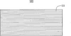
所述第一透明导电层122与第二透明导电层142的材料具有透明可导电的特性,如ITO、ATO、碳纳米管膜、碳纳米管金属复合层等。其中,该第一透明导电层122与第二透明导电层142中至少一个透明导电层为所述碳纳米管金属复合层100,该碳纳米管金属复合层100包括碳纳米管和金属层,且每个碳纳米管表面均包覆一金属层。其中,每个碳纳米管具有大致相等的长度;所述金属层包括润湿层、导电层、抗氧化层中的至少一层。所述金属层的厚度为1纳米~50纳米。所述碳纳米管金属复合层100的厚度约为1.5纳米~1毫米。所述碳纳米管金属复合层100的方块电阻为50欧~2000欧,可见光透过率为80%-95%。其中,所述光透过率是指所述碳纳米管金属复合层100对550纳米的光的透过率。所述金属层的材料包括铜、银、金、铁、钴、镍、钯、钛、铂或其任意组合的合金。The materials of the first transparent
所述碳纳米管金属复合层100包括一碳纳米管层及包覆于该碳纳米管层表面的一金属层。具体地,所述碳纳米管层包括多个碳纳米管通过范德华力相互作用组成一自支撑结构,所述金属层包覆于所述碳纳米管层中的每个碳纳米管的表面。所述碳纳米管层包括一层碳纳米管膜或至少两层碳纳米管膜,且该至少两层碳纳米管膜并排设置或层叠设置。所述碳纳米管膜包括多个碳纳米管基本相互平行且平行于该碳纳米管膜的表面,该多个碳纳米管通过范德华力首尾相连且基本沿同一方向择优取向排列。The carbon nanotube
所谓“自支撑”即该碳纳米管膜无需通过一支撑体支撑,也能保持自身特定的形状。该自支撑的碳纳米管膜包括多个碳纳米管,该多个碳纳米管通过范德华力相互吸引并首尾相连,从而使碳纳米管膜具有特定的形状。The so-called "self-supporting" means that the carbon nanotube film can maintain its own specific shape without being supported by a support body. The self-supporting carbon nanotube film includes a plurality of carbon nanotubes, and the plurality of carbon nanotubes are attracted to each other and connected end to end through van der Waals force, so that the carbon nanotube film has a specific shape.
所述碳纳米管金属复合层100包括多个碳纳米管金属复合线状结构相互连接组成一网状结构。所述碳纳米管金属复合线状结构包括至少一碳纳米管线及包覆于该至少一碳纳米管线表面的金属层。当所述碳纳米管金属复合线状结构包括至少两个碳纳米管线时,该至少两个碳纳米管线并排设置或交叉设置,且至少一个碳纳米管线的表面包覆一金属层。所述碳纳米管线包括多个碳纳米管,该多个碳纳米管通过范德华力首尾相连且沿着该碳纳米管线的轴向择优取向排列或螺旋排列。其中,所述碳纳米管线中的每个碳纳米管的表面包覆一金属层。另外,所述碳纳米管金属复合线状结构也包括至少一金属纳米线以及复合于该至少一金属纳米线内部的碳纳米管。当所述碳纳米管金属复合线状结构包括至少两个金属纳米线,该至少两个金属纳米线并排设置或交叉设置,且至少有一个金属纳米线的内部复合有碳纳米管。The carbon nanotube
本实施例中,所述碳纳米管金属复合膜包括一层碳纳米管膜及包覆于该碳纳米管膜表面的金属层。具体地,请参阅图3,所述碳纳米管金属复合层100包括多个均匀分布的碳纳米管111,该多个碳纳米管111组成一自支撑的碳纳米管膜。并且,每个碳纳米管111表面均包覆一金属层。在该碳纳米管金属复合层100中,碳纳米管111沿同一个方向择优取向排列。碳纳米管金属复合层100中的每个碳纳米管111具有大致相等的长度,且通过范德华力首尾相连。In this embodiment, the carbon nanotube-metal composite film includes a layer of carbon nanotube film and a metal layer coated on the surface of the carbon nanotube film. Specifically, referring to FIG. 3 , the carbon nanotube-
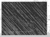
请参见图4及图5,该碳纳米管金属复合层100中每一根碳纳米管111表面均包覆与碳纳米管111表面直接结合的润湿层112,以及设置在润湿层112外的导电层114。4 and 5, the surface of each
由于碳纳米管111与大多数金属之间的润湿性不好,因此,所述润湿层112的作用为使导电层114与碳纳米管111更好的结合。形成该润湿层112的材料可以为铁、钴、镍、钯或钛等与碳纳米管111润湿性好的金属或它们的合金,该润湿层112的厚度为1~10纳米。本实施例中,该润湿层112的材料为镍,厚度约为2纳米。可以理解,该润湿层为可选择结构。Since the wettability between the
所述导电层114的作用为使碳纳米管金属复合层100具有较好的导电性能。形成该导电层114的材料可以为铜、银或金等导电性好的金属或它们的合金,该导电层114的厚度为1~20纳米。本实施例中,该导电层114的材料为金,厚度约为10纳米。The function of the
本实施例中,该碳纳米管金属复合层100包括多个碳纳米管111,每个碳纳米管111的表面包括厚度为2纳米的镍润湿层112、厚度为10纳米的金导电层114。该碳纳米管金属复合层100的方块电阻为1173欧姆,波长为550纳米的光的透光率为92.7%。In this embodiment, the carbon nanotube
可以理解,所述碳纳米管金属复合层100的方块电阻及透光率与该碳纳米管金属复合层100的结构及厚度有关。如,当该碳纳米管金属复合层100中的每个碳纳米管111的表面包括厚度为2纳米的镍润湿层、厚度为15纳米的金导电层时,该碳纳米管金属复合层100的方块电阻为495欧姆,波长为550纳米的光的透光率为90.7%。当该碳纳米管金属复合层100中的每个碳纳米管111的表面包括厚度为2纳米的镍润湿层、厚度为20纳米的金导电层;该碳纳米管金属复合层100的方块电阻为208欧姆,波长为550纳米的光的透光率为89.7%。It can be understood that the sheet resistance and light transmittance of the carbon nanotube
该第一实施例中,所述第一透明导电层122和第二透明导电层142都为碳纳米管金属复合层100。由于碳纳米管本身的比表面积非常大,所以该碳纳米管金属复合层本身也具有较强的粘性。因此,本实施例中,该碳纳米管金属复合层作为第一透明导电层122与第二透明导电层142时可直接黏附在第一基体120以及第二基体140上。In the first embodiment, both the first transparent
另外,可使用有机溶剂处理上述黏附在第一基体120以及第二基体140上的碳纳米管金属复合层。具体地,可通过试管将有机溶剂滴落在碳纳米管金属复合层表面浸润整个碳纳米管金属复合层。该有机溶剂为挥发性有机溶剂,如乙醇、甲醇、丙酮、二氯乙烷或氯仿,本实施例中采用乙醇。该碳纳米管金属复合层经有机溶剂浸润处理后,在挥发性有机溶剂的表面张力的作用下,该碳纳米管金属复合层可牢固地贴附在基体表面,且该碳纳米管金属复合层比表面积减小,粘性降低,具有良好的机械强度及韧性。In addition, an organic solvent can be used to treat the carbon nanotube-metal composite layer adhered to the
可以理解,所述碳纳米管金属复合层100也可以通过黏胶黏附在第一基体120以及第二基体140上。It can be understood that the carbon nanotube
所述多个点状隔离物16设置在第二电极板14的第二透明导电层142上,且该多个点状隔离物16彼此间隔设置。所述绝缘框架18设置于所述第一电极板12的第一表面与第二电极板18的第二表面之间。所述多个点状隔离物16与绝缘框架18均可采用绝缘树脂或其他绝缘材料制成,并且,该点状隔离物16应为一透明材料制成。所述多个点状隔离物16与绝缘框架18可使第一电极板14与第二电极板12电绝缘。可以理解,当触摸屏10尺寸较小时,该多个点状隔离物16为可选择的结构,只要该绝缘框架18能确保所述第一电极板14与第二电极板12电绝缘即可。The plurality of
所述屏蔽层146设置于所述第二基体140远离绝缘框架18的一个表面。该屏蔽层146是为了减小由显示设备产生的电磁干扰,避免从触摸屏10发出的信号产生错误。该屏蔽层146可由碳纳米管膜、碳纳米管金属复合层、导电聚合物薄膜等导电材料形成。本实施例中,所述的屏蔽层146包含一碳纳米管膜,该碳纳米管膜中的碳纳米管的排列方式不限,可为定向排列也可为其他的排列方式。本实施例中,该屏蔽层146中的碳纳米管定向排列,该屏蔽层146作为电接地点,起到屏蔽的作用,从而使得触摸屏10能在无干扰的环境中工作。可以理解,该屏蔽层146为可选择结构。The
另外,该触摸屏10进一步包括一透明保护膜126,该透明保护膜126设置于所述第一电极板12远离第一透明导电层122的表面。所述透明保护膜126可以通过粘结剂直接粘结在所述第一电极板12上,也可采用热压法与该第一电极板12压合在一起。所述透明保护膜126可采用一层经过表面硬化处理、光滑防刮的塑料层或树脂层,该树脂层可由苯丙环丁烯(BCB)、聚酯以及丙烯酸树脂等材料形成。本实施例中,形成该透明保护膜126的材料为聚对苯二甲酸乙二醇酯(PET),用于保护第一电极板12,提高耐用性。该透明保护膜126经特殊工艺处理后,可用以提供一些附加功能,如可以减少眩光或降低反射。In addition, the
可以理解,所述两个第一电极124可以不设置在所述第一电极板12上,而是与所述两个第二电极144一起设置于所述第二电极板14。具体地,该两个第一电极124沿第一方向间隔设置于所述第二透明导电层142的表面,两个第二电极144沿第二方向间隔设置于所述第二透明导电层142的表面,且该两个第一电极124及两个第二电极144与该第二透明导电层142电连接,所述第一方向与第二方向相交。It can be understood that the two
本发明第二实施例提供一种触摸屏,该触摸屏与第一实施例中的触摸屏100的结构基本相同,只是本实施例中的第一透明导电层及第二透明导电层的结构与第一实施例中的第一透明导电层122及第二透明导电层142的结构不同。The second embodiment of the present invention provides a touch screen, the structure of the touch screen is basically the same as that of the
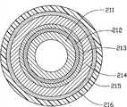
该第二实施例中第一透明导电层与第二透明导电层为一碳纳米管金属复合层,该碳纳米管金属复合膜包括碳纳米管膜和金属层。所述碳纳米管金属复合层包括多个碳纳米管,具体地,请参阅图6,该碳纳米管金属复合层中的每一根碳纳米管211表面均包覆与碳纳米管211表面直接结合的润湿层212、设置在润湿层外的过渡层213、设置在过渡层213外的导电层214、设置在导电层214外的抗氧化层215以及设置在该抗氧化层215外的强化层216。In the second embodiment, the first transparent conductive layer and the second transparent conductive layer are a carbon nanotube-metal composite layer, and the carbon nanotube-metal composite film includes a carbon nanotube film and a metal layer. The carbon nanotube metal composite layer includes a plurality of carbon nanotubes. Specifically, please refer to FIG. The combined
由于碳纳米管211与大多数金属之间的润湿性不好,因此,所述润湿层212的作用为使导电层214与碳纳米管211更好的结合。形成该润湿层212的材料可以为铁、钴、镍、钯或钛等与碳纳米管211润湿性好的金属或它们的合金,该润湿层212的厚度为1~10纳米。本实施例中,该润湿层212的材料为钛,厚度约为2纳米。可以理解,该润湿层为可选择结构。Since the wettability between the
所述过渡层213的作用为使润湿层212与导电层214更好的结合。形成该过渡层213的材料为与润湿层212材料及导电层214材料均能较好结合的材料,该过渡层213的厚度为1~10纳米。本实施例中,该过渡层213的材料为铜,厚度为2纳米。可以理解,该过渡层213为可选择结构。The function of the
所述导电层214的作用为使碳纳米管金属复合层具有较好的导电性能。形成该导电层214的材料可以为铜、银或金等导电性好的金属或它们的合金,该导电层214的厚度为1~20纳米。本实施例中,该导电层214的材料为银,厚度约为10纳米。The function of the conductive layer 214 is to make the carbon nanotube metal composite layer have better conductivity. The material forming the conductive layer 214 may be copper, silver or gold and other metals with high conductivity or their alloys, and the thickness of the conductive layer 214 is 1-20 nanometers. In this embodiment, the material of the conductive layer 214 is silver, and the thickness is about 10 nanometers.
所述抗氧化层215的作用为防止在碳纳米管金属复合层的制造过程中,导电层214在空气中被氧化,从而降低碳纳米管金属复合层的导电性。形成该抗氧化层215的材料可以为金或铂等在空气中不易氧化的稳定金属或它们的合金,该抗氧化层215的厚度为1~10纳米。本实施例中,该抗氧化层115的材料为铂,厚度为2纳米。可以理解,该抗氧化层215为可选择结构。The function of the
所述强化层216用以提高碳纳米管金属复合层的强度。形成该强化层216的材料可以为聚乙烯醇(PVA)、聚苯撑苯并二噁唑(PBO)、聚乙烯(PE)或聚氯乙烯(PVC)等强度较高的聚合物,该强化层216的厚度为0.1~1微米。本实施例中,该强化层216的材料为聚乙烯醇(PVA),厚度为0.2微米。可以理解,该强化层216为可选择结构。The
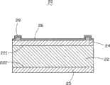
请参阅图7及图8,本发明第三实施例提供一触摸屏20,该触摸屏20包括一基体22、一透明导电层24、至少四个电极28、一屏蔽层25及一透明保护膜26。该基体22具有一第一表面221以及与第一表面221相对的第二表面222。该透明导电层24设置在基体22的第一表面221上;所述至少四个电极28分别设置在所述透明导电层24的四个角处或边缘上,且与透明导电层24形成电连接,用以在透明导电层24上形成等电位面。所述屏蔽层25设置于所述基体22的第二表面222上。所述透明保护膜26可直接设置在透明导电层24以及电极28上。7 and 8, the third embodiment of the present invention provides a
所述基体22为一曲面型或平面型的结构。该基体22由玻璃、石英、金刚石或塑料等硬性材料或柔性材料形成。所述柔性材料的范围与第一实施例中第一基体120的柔性材料的范围相同。所述基体22主要起支撑的作用。本实施例中,所述基体22为一平面型的结构,该基体22为柔性材料聚碳酸酯(PC)。The
所述透明导电层24包括一碳纳米管金属复合层,该碳纳米管金属复合层的材料包括碳纳米管和金属导电材料。具体地,所述碳纳米管金属复合层的结构可以与第一实施例中第一透明导电层122和第二透明导电层142中的碳纳米管金属复合层的结构相同;也可以与第二实施例中的第一透明导电层和第二透明导电层中的碳纳米管复合层的结构相同。本实施例中所述的碳纳米管金属复合层的结构与第一实施例中的第一透明导电层122和第二透明导电层142中的碳纳米管金属复合层的结构相同。The transparent
具体地,可以采用四个电极28分别设置于透明导电层24的四个角或四条边上,用以在上述的透明导电层24上形成均匀的电阻网络。在本实施例中,四个带状电极28间隔设置在上述的透明导电层24同一表面的四个边上。可以理解,上述的电极28也可以设置在透明导电层24的不同表面上,其关键在于上述电极28的设置能使得在透明导电层24上形成等电位面即可。本实施例中,所述电极28设置在透明导电层24的远离基体22的一个表面上。Specifically, four
可以理解,所述的四个电极28也可设置于透明导电层24与基体22之间,且与透明导电层24电连接。It can be understood that the four
所述四个电极28的材料为金属、碳纳米管膜、碳纳米管金属复合层或其他导电材料,只要确保该四个电极28能导电即可。本实施例中,所述四个电极28为由银或铜等低电阻的导电金属镀层或者金属箔片组成的条状电极28。The materials of the four
所述屏蔽层25与第一实施例中的屏蔽层146的材料及作用相同。The material and function of the
所述透明保护膜26可由氮化硅、氧化硅、苯丙环丁烯(BCB)、聚酯膜或丙烯酸树脂等形成。该透明保护膜26具有一定的硬度,对透明导电层24起保护作用。可以理解,还可通过特殊的工艺处理,从而使得透明保护膜26具有以下功能,例如减小炫光、降低反射等。在本实施例中,在透明导电层24形成有电极28的表面设置一二氧化硅层用作透明保护膜26,该透明保护膜26的硬度可达到7H(H为洛氏硬度试验中,卸除主试验力后,在初试验力下压痕残留的深度)。可以理解,透明保护膜26的硬度和厚度可以根据需要进行选择。所述透明保护膜26可以通过粘结剂直接粘结在透明导电层24及电极28远离基体22的表面。可以理解,该透明保护膜26是可选择结构。The transparent
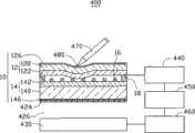
请参阅图9,图9为采用第一实施例的触摸屏10的显示装置400,其包括一触摸屏10、一显示设备430、一摸屏控制器440、一中央处理器450及一显示设备控制器460。其中,该触摸屏控制器440、该中央处理器450及该显示设备控制器460三者通过电路相互连接,该触摸屏控制器440与该触摸屏10电连接,该显示设备控制器460与该显示设备430电连接。该触摸屏控制器440通过手指等触摸物470触摸的图标或菜单来选择信息输入,并将该信息传递给中央处理器450。该中央处理器450通过该显示设备控制器460控制该显示设备430显示。所述显示设备430正对且靠近所述触摸屏10的第二电极板14设置。Please refer to FIG. 9, FIG. 9 is a
所述触摸屏10可以与该显示设备430间隔设置,也可集成在该显示设备430上。当该触摸屏10与该显示设备430集成设置时,可通过粘结剂将该触摸屏10附着到该显示设备430上。当该显示设备430与该触摸屏10间隔设置时,可在该触摸屏10的屏蔽层146远离第二基体140的表面上设置一钝化层424,该钝化层424可由苯并环丁烯(BCB)、聚酯或丙烯酸树脂等柔性材料形成。该钝化层424与显示设备430的正面间隔一间隙426设置。该钝化层424作为介电层使用,且可以保护该显示设备430不致于由于外力过大而损坏。The
所述显示设备430可以为液晶显示器、场发射显示器、等离子显示器、电致发光显示器、真空荧光显示器及阴极射线管等传统显示设备中的一种,另外,该显示设备430也可为一柔性液晶显示器、柔性电泳显示器、柔性有机电致发光显示器等柔性显示器中的一种。本实施例中,所述显示设备430为液晶显示器。The
使用时,在第一电极板12第二电极板14分别施加一电压。使用者一边视觉确认在触摸屏10下面设置的显示设备430的显示,一边通过触摸物470如手指或笔按压触摸屏10的第一电极板12进行操作。所述第一电极板12中第一基体120受力发生弯曲,使得按压处480的第一电极板12的第一透明导电层122与第二电极板14的第二透明导电层142接触导通。触摸屏控制器440通过分别测量第一透明导电层122在X方向上的电压变化与第二透明导电层142在Y方向上的电压变化,并进行精确计算,将它转换成触点坐标。触摸屏控制器440将数字化的触点坐标传递给中央处理器450。中央处理器450根据触点坐标发出相应指令,启动电子设备的各种功能切换,并通过显示设备控制器460控制显示设备430显示。In use, a voltage is respectively applied to the
请参阅图10,图10为采用第三实施例的触摸屏20的显示装置500。该显示装置500包括一触摸屏20、一显示设备530、触摸屏控制器540、一中央处理器550及一显示设备控制器560。其中,触摸屏控制器540、中央处理器550及显示设备控制器560三者通过电路相互连接,触摸屏控制器540连接触摸屏20的电极28,显示设备控制器560连接显示设备530。该显示设备530正对且靠近触摸屏20设置。Please refer to FIG. 10 . FIG. 10 is a
所述显示设备530正对且靠近触摸屏20的屏蔽层25设置。该显示设备530与触摸屏20可间隔设置或集成设置。当显示设备530与触摸屏20间隔设置时,可在触摸屏20的屏蔽层25远离基体22的一个表面上设置一钝化层524,该钝化层524可由苯并环丁烯(BCB)、聚酯或丙烯酸树脂等柔性材料形成。该钝化层524与显示设备530的显示面之间设置有一间隙526。具体地,在上述的钝化层524与显示设备530之间设置支撑体528。该钝化层524作为介电层使用,所述钝化层524与间隙526可保护显示设备530不致于由于外力过大而损坏。当显示设备530与触摸屏20集成设置时,触摸屏20和显示设备530之间接触设置。即将支撑体528除去后,上述钝化层524无间隙地设置在显示设备530的显示面。The
所述显示设备530的类型与本发明提供的显示装置的第一实施例提供的显示装置400中的显示设备430的类型相同。The type of the
本实施例触摸屏20及显示装置500在应用时的原理如下:触摸屏20在应用时可直接设置在显示设备530的显示面上。触摸屏控制器540根据手指等触摸物570触摸的图标或菜单来选择信息输入,并将该信息传递给中央处理器550。中央处理器550通过显示器控制器560控制显示设备530显示。The principle of the application of the
具体地,在使用时,通过在电极28施加一预定电压到透明导电层24上,从而在该透明导电层24上形成等电位面。使用者一边视觉确认在触摸屏20后面设置的显示设备530的显示,一边通过手指或笔等触摸物570按压或接近触摸屏20的透明保护层26进行操作时,触摸物570与透明导电层24之间形成一耦合电容。对于高频电流来说,电容是直接导体,于是手指从接触点吸走了一部分电流。这个电流分别从触摸屏20上的电极28中流出,并且流经这四个电极28的电流与手指到四角的距离成正比,触摸屏控制器540通过对这四个电流比例的精确计算,得出触摸点的位置。之后,触摸屏控制器540将数字化的触摸位置数据传送给中央处理器550。然后,中央处理器550接收上述的触摸位置数据并执行。最后,中央处理器550将该触摸位置数据传输给显示器控制器560,从而在显示设备530上显示接触物570发出的触摸信息。Specifically, when in use, an equipotential surface is formed on the transparent
可以理解,本发明提供的触摸屏的第二实施例也可以用于上述的显示装置中。It can be understood that the second embodiment of the touch screen provided by the present invention can also be used in the above-mentioned display device.
本发明实施例提供的采用碳纳米管金属复合层作为透明导电层的触摸屏及使用该触摸屏的显示装置具有以下优点:第一,由于碳纳米管及金属具有较好的力学性能,则由碳纳米管和金属组成的碳纳米管金属复合层具有较好的韧性及机械强度,并且耐弯折,故,可以相应的提高触摸屏的耐用性,进而提高使用该触摸屏的显示装置的耐用性;第二,由于该碳纳米管金属复合层具有较高的透光性,可以提高触摸屏的透明度,进而提高使用该触摸屏的显示装置的透明度;第三,由于碳纳米管金属复合层包括多个均匀分布的碳纳米管,且碳纳米管具有优异的导电性能,另外,该碳纳米管金属复合层中的每个碳纳米管表面均形成有金属导电材料,该金属导电材料具有较好的导电性能,因此,该碳纳米管金属复合层具有较好的导电性,较低的电阻率,均匀的阻值分布,因而,采用上述碳纳米管金属复合层作透明导电层,可以相应的提高触摸屏的灵敏度和精确度,进而提高应用该触摸屏的显示器件的灵敏度和精确度;第四,本发明实施中的基体的材料为柔性材料时,可以制备一柔性触摸屏,从而适合用于柔性显示装置。The touch screen using the carbon nanotube metal composite layer as the transparent conductive layer and the display device using the touch screen provided by the embodiments of the present invention have the following advantages: First, since carbon nanotubes and metals have better mechanical properties, carbon nanotubes The carbon nanotube metal composite layer composed of tubes and metals has good toughness and mechanical strength, and is resistant to bending, so the durability of the touch screen can be improved accordingly, and then the durability of the display device using the touch screen can be improved; the second , because the carbon nanotube metal composite layer has high light transmittance, the transparency of the touch screen can be improved, and then the transparency of the display device using the touch screen can be improved; thirdly, since the carbon nanotube metal composite layer includes a plurality of evenly distributed Carbon nanotubes, and carbon nanotubes have excellent electrical conductivity, in addition, the surface of each carbon nanotube in the carbon nanotube metal composite layer is formed with a metal conductive material, and the metal conductive material has good electrical conductivity, so , the carbon nanotube metal composite layer has good conductivity, low resistivity, and uniform resistance value distribution. Therefore, using the above carbon nanotube metal composite layer as a transparent conductive layer can correspondingly improve the sensitivity and sensitivity of the touch screen. Accuracy, and then improve the sensitivity and accuracy of the display device using the touch screen; Fourth, when the material of the substrate in the implementation of the present invention is a flexible material, a flexible touch screen can be prepared, which is suitable for flexible display devices.
另外,本领域技术人员还可以在本发明精神内做其他变化,这些依据本发明精神所做的变化,都应包含在本发明所要求保护的范围内。In addition, those skilled in the art can also make other changes within the spirit of the present invention, and these changes made according to the spirit of the present invention should be included in the scope of protection claimed by the present invention.
Claims (17)
Priority Applications (3)
| Application Number | Priority Date | Filing Date | Title |
|---|---|---|---|
| CN2009101095690ACN101989136B (en) | 2009-08-07 | 2009-08-07 | Touch screen and display device |
| US12/655,489US8766927B2 (en) | 2009-08-07 | 2009-12-31 | Touch panel and display device using the same |
| JP2010150836AJP5345979B2 (en) | 2009-08-07 | 2010-07-01 | Touch panel and display using the same |
Applications Claiming Priority (1)
| Application Number | Priority Date | Filing Date | Title |
|---|---|---|---|
| CN2009101095690ACN101989136B (en) | 2009-08-07 | 2009-08-07 | Touch screen and display device |
Publications (2)
| Publication Number | Publication Date |
|---|---|
| CN101989136A CN101989136A (en) | 2011-03-23 |
| CN101989136Btrue CN101989136B (en) | 2012-12-19 |
Family
ID=43534458
Family Applications (1)
| Application Number | Title | Priority Date | Filing Date |
|---|---|---|---|
| CN2009101095690AActiveCN101989136B (en) | 2009-08-07 | 2009-08-07 | Touch screen and display device |
Country Status (3)
| Country | Link |
|---|---|
| US (1) | US8766927B2 (en) |
| JP (1) | JP5345979B2 (en) |
| CN (1) | CN101989136B (en) |
Families Citing this family (69)
| Publication number | Priority date | Publication date | Assignee | Title |
|---|---|---|---|---|
| CN101419518B (en)* | 2007-10-23 | 2012-06-20 | 清华大学 | Touch panel |
| CN101470559B (en) | 2007-12-27 | 2012-11-21 | 清华大学 | Touch screen and display equipment |
| CN101470566B (en) | 2007-12-27 | 2011-06-08 | 清华大学 | Touch control device |
| CN101458605B (en)* | 2007-12-12 | 2011-03-30 | 鸿富锦精密工业(深圳)有限公司 | Touch screen and display device |
| CN101470558B (en) | 2007-12-27 | 2012-11-21 | 清华大学 | Touch screen and display equipment |
| CN101464763B (en) | 2007-12-21 | 2010-09-29 | 清华大学 | Manufacturing method of touch screen |
| CN101458593B (en) | 2007-12-12 | 2012-03-14 | 清华大学 | Touch screen and display device |
| CN101458596B (en) | 2007-12-12 | 2011-06-08 | 北京富纳特创新科技有限公司 | Touch screen and display device |
| CN101655720B (en) | 2008-08-22 | 2012-07-18 | 清华大学 | Personal digital assistant |
| CN101458600B (en) | 2007-12-14 | 2011-11-30 | 清华大学 | Touch screen and display device |
| CN101458594B (en) | 2007-12-12 | 2012-07-18 | 清华大学 | Touch screen and display device |
| CN101458604B (en) | 2007-12-12 | 2012-03-28 | 清华大学 | Touch screen and display device |
| CN101419519B (en)* | 2007-10-23 | 2012-06-20 | 清华大学 | Touch panel |
| CN101458595B (en) | 2007-12-12 | 2011-06-08 | 清华大学 | Touch screen and display device |
| CN101470560B (en)* | 2007-12-27 | 2012-01-25 | 清华大学 | Touch screen and display equipment |
| CN101458602B (en) | 2007-12-12 | 2011-12-21 | 清华大学 | Touch screen and display device |
| CN101458598B (en) | 2007-12-14 | 2011-06-08 | 清华大学 | Touch screen and display device |
| CN101458603B (en)* | 2007-12-12 | 2011-06-08 | 北京富纳特创新科技有限公司 | Touch screen and display device |
| CN101458608B (en)* | 2007-12-14 | 2011-09-28 | 清华大学 | Touch screen preparation method |
| CN101458599B (en) | 2007-12-14 | 2011-06-08 | 清华大学 | Touch screen, method for producing the touch screen, and display device using the touch screen |
| CN101458609B (en)* | 2007-12-14 | 2011-11-09 | 清华大学 | Touch screen and display device |
| CN101458606B (en)* | 2007-12-12 | 2012-06-20 | 清华大学 | Touch screen, method for producing the touch screen, and display device using the touch screen |
| CN101458597B (en) | 2007-12-14 | 2011-06-08 | 清华大学 | Touch screen, method for producing the touch screen, and display device using the touch screen |
| CN101656769B (en) | 2008-08-22 | 2012-10-10 | 清华大学 | Mobile telephone |
| CN101458975B (en) | 2007-12-12 | 2012-05-16 | 清华大学 | Electronic element |
| CN101458601B (en) | 2007-12-14 | 2012-03-14 | 清华大学 | Touch screen and display device |
| CN101464757A (en) | 2007-12-21 | 2009-06-24 | 清华大学 | Touch screen and display equipment |
| CN101458607B (en)* | 2007-12-14 | 2010-12-29 | 清华大学 | Touch screen and display device |
| CN101470565B (en) | 2007-12-27 | 2011-08-24 | 清华大学 | Touch screen and display device |
| US8574393B2 (en) | 2007-12-21 | 2013-11-05 | Tsinghua University | Method for making touch panel |
| CN101464766B (en)* | 2007-12-21 | 2011-11-30 | 清华大学 | Touch screen and display equipment |
| CN101464765B (en) | 2007-12-21 | 2011-01-05 | 鸿富锦精密工业(深圳)有限公司 | Touch screen and display equipment |
| CN101464764B (en)* | 2007-12-21 | 2012-07-18 | 清华大学 | Touch screen and display equipment |
| US8237677B2 (en) | 2008-07-04 | 2012-08-07 | Tsinghua University | Liquid crystal display screen |
| US8390580B2 (en) | 2008-07-09 | 2013-03-05 | Tsinghua University | Touch panel, liquid crystal display screen using the same, and methods for making the touch panel and the liquid crystal display screen |
| CN101924816B (en) | 2009-06-12 | 2013-03-20 | 清华大学 | Flexible mobile phone |
| CN101989136B (en)* | 2009-08-07 | 2012-12-19 | 清华大学 | Touch screen and display device |
| US20110221676A1 (en)* | 2010-03-11 | 2011-09-15 | Sunrex Technology Corp. | Optical mouse with touch sensitive top |
| CN102193693B (en)* | 2010-03-17 | 2014-03-19 | 群康科技(深圳)有限公司 | Touch panel and differential identification method thereof |
| CN101880035A (en) | 2010-06-29 | 2010-11-10 | 清华大学 | carbon nanotube structure |
| CN103003781B (en)* | 2010-07-14 | 2016-08-17 | Lg伊诺特有限公司 | Touch panel and manufacture method thereof |
| TW201239496A (en)* | 2011-03-18 | 2012-10-01 | Shih Hua Technology Ltd | Touch-control e-paper display |
| FR2973263B1 (en)* | 2011-03-28 | 2013-08-02 | Commissariat Energie Atomique | ELABORATION OF TRANSPARENT ELECTRODES IN METALLIZED CARBON NANOTUBES |
| TWI528388B (en)* | 2011-06-09 | 2016-04-01 | 識驊科技股份有限公司 | Pattern conductive element |
| CN102866811A (en)* | 2011-07-06 | 2013-01-09 | 安浙触控科技有限公司 | capacitive touch panel |
| US20130022756A1 (en)* | 2011-07-20 | 2013-01-24 | Brian Howard Augustine | Adhesion of metal thin films to polymeric substratres |
| CN102981657B (en)* | 2011-09-05 | 2016-03-02 | 天津富纳源创科技有限公司 | Touch type electronic paper display |
| CN102999199B (en)* | 2011-09-16 | 2016-08-10 | 宸鸿科技(厦门)有限公司 | Touch sensing device and electronic installation |
| CN103164058B (en)* | 2011-12-09 | 2016-02-17 | 上海天马微电子有限公司 | Touch screen, color filter substrate and liquid crystal display |
| US20140054076A1 (en)* | 2012-04-19 | 2014-02-27 | Shenzhen O-Film Tech Co., Ltd. | Conductive component and preparation method thereof |
| TWI483271B (en)* | 2012-05-29 | 2015-05-01 | Shih Hua Technology Ltd | Touch panel |
| CN103455184A (en)* | 2012-05-30 | 2013-12-18 | 天津富纳源创科技有限公司 | Touch panel |
| KR101926598B1 (en) | 2012-06-29 | 2018-12-11 | 엘지이노텍 주식회사 | Touch panel |
| CN103576356A (en)* | 2012-07-23 | 2014-02-12 | 天津富纳源创科技有限公司 | Production method for liquid crystal module having touch function |
| CN103576352A (en)* | 2012-07-23 | 2014-02-12 | 天津富纳源创科技有限公司 | LCD (Liquid Crystal Display) module with touch function |
| CN103576351A (en)* | 2012-07-23 | 2014-02-12 | 天津富纳源创科技有限公司 | Liquid crystal module having touch function |
| CN103631456B (en) | 2012-08-24 | 2017-07-04 | 深圳欧菲光科技股份有限公司 | Film inductor, the capacitance touch screen comprising the inductor and preparation method thereof and end product |
| KR101934310B1 (en) | 2012-08-24 | 2019-01-03 | 삼성디스플레이 주식회사 | touch display apparatus sensing touch force |
| US9510456B2 (en) | 2012-11-09 | 2016-11-29 | Shenzhen O-Film Tech Co., Ltd. | Transparent conductor and preparation method thereof |
| CN103809342A (en)* | 2012-11-15 | 2014-05-21 | 广州奥翼电子科技有限公司 | Display device with touch function and manufacturing method of display device |
| CN103838440B (en)* | 2012-11-23 | 2016-08-10 | 北京富纳特创新科技有限公司 | Touch screen |
| CN103838441B (en)* | 2012-11-23 | 2016-09-28 | 北京富纳特创新科技有限公司 | Capacitive touch screen |
| US20140320756A1 (en)* | 2013-04-26 | 2014-10-30 | Tianjin Funayuanchuang Technology Co.,Ltd. | Touch panel |
| US9632542B2 (en)* | 2013-05-02 | 2017-04-25 | The Boeing Company | Touch screens comprising graphene layers |
| CN105094390B (en)* | 2014-04-23 | 2018-07-13 | 北京富纳特创新科技有限公司 | Conductive grid and touch panel |
| FR3020742B1 (en)* | 2014-05-05 | 2016-05-27 | Valeo Systemes De Controle Moteur | ELECTRICAL SYSTEM WITH SHIELD |
| US9485862B2 (en)* | 2014-08-28 | 2016-11-01 | Apple Inc. | Electronic devices with carbon nanotube printed circuits |
| CN105807971B (en)* | 2014-12-31 | 2019-01-18 | 清华大学 | Electrostatic transducer |
| CN105808030B (en)* | 2014-12-31 | 2018-10-02 | 清华大学 | Electrostatic transducer |
Citations (7)
| Publication number | Priority date | Publication date | Assignee | Title |
|---|---|---|---|---|
| CN101255590A (en)* | 2008-04-03 | 2008-09-03 | 厦门大学 | A kind of preparation method of carbon nanotube/nano-platinum composite film material |
| CN101458600A (en)* | 2007-12-14 | 2009-06-17 | 清华大学 | Touch screen and display device |
| CN101458598A (en)* | 2007-12-14 | 2009-06-17 | 清华大学 | Touch screen and display device |
| CN101458597A (en)* | 2007-12-14 | 2009-06-17 | 清华大学 | Touch screen, method for producing the touch screen, and display device using the touch screen |
| CN101458607A (en)* | 2007-12-14 | 2009-06-17 | 清华大学 | Touch screen and display device |
| CN101458606A (en)* | 2007-12-12 | 2009-06-17 | 清华大学 | Touch screen, method for producing the touch screen, and display device using the touch screen |
| CN101499337A (en)* | 2008-02-01 | 2009-08-05 | 清华大学 | Cable production method |
Family Cites Families (17)
| Publication number | Priority date | Publication date | Assignee | Title |
|---|---|---|---|---|
| US5507856A (en) | 1989-11-14 | 1996-04-16 | Air Products And Chemicals, Inc. | Hydrogen recovery by adsorbent membranes |
| JP2953996B2 (en) | 1995-05-31 | 1999-09-27 | 日本電気株式会社 | Metal-coated carbon nanotube and method for producing the same |
| JP2002025477A (en)* | 2000-07-07 | 2002-01-25 | Ise Electronics Corp | Surface display and its manufacturing method |
| CN1281982C (en)* | 2002-09-10 | 2006-10-25 | 清华大学 | Polarized element and method for manufacturing same |
| JP2005104141A (en)* | 2003-09-11 | 2005-04-21 | Teijin Ltd | Transparent conductive laminate and transparent touch panel |
| WO2005104141A1 (en)* | 2004-04-20 | 2005-11-03 | Takiron Co., Ltd. | Touch panel-use transparent conductive molded product and touch panel |
| CN105696139B (en) | 2004-11-09 | 2019-04-16 | 得克萨斯大学体系董事会 | The manufacture and application of nano-fibre yams, band and plate |
| US20060231946A1 (en)* | 2005-04-14 | 2006-10-19 | Molecular Nanosystems, Inc. | Nanotube surface coatings for improved wettability |
| EP2477230B1 (en) | 2005-08-12 | 2015-02-25 | Cambrios Technologies Corporation | Nanowires-based transparent conductors on a flexible donor substrate |
| JP2008038764A (en)* | 2006-08-07 | 2008-02-21 | Shimadzu Corp | Turbomolecular pump and power supply device therefor |
| EP2068328B1 (en)* | 2006-09-28 | 2014-10-22 | FUJIFILM Corporation | Spontaneous emission display and transparent conductive film |
| JP4287461B2 (en)* | 2006-11-17 | 2009-07-01 | 日精樹脂工業株式会社 | Method for producing carbon nanocomposite metal material and method for producing carbon nanocomposite metal molded product |
| JP2008145208A (en)* | 2006-12-08 | 2008-06-26 | Hitachi High-Technologies Corp | Semiconductor inspection equipment |
| WO2008127780A2 (en) | 2007-02-21 | 2008-10-23 | Nantero, Inc. | Symmetric touch screen system with carbon nanotube-based transparent conductive electrode pairs |
| CN101470566B (en) | 2007-12-27 | 2011-06-08 | 清华大学 | Touch control device |
| CN101470560B (en)* | 2007-12-27 | 2012-01-25 | 清华大学 | Touch screen and display equipment |
| CN101989136B (en)* | 2009-08-07 | 2012-12-19 | 清华大学 | Touch screen and display device |
- 2009
- 2009-08-07CNCN2009101095690Apatent/CN101989136B/enactiveActive
- 2009-12-31USUS12/655,489patent/US8766927B2/enactiveActive
- 2010
- 2010-07-01JPJP2010150836Apatent/JP5345979B2/enactiveActive
Patent Citations (7)
| Publication number | Priority date | Publication date | Assignee | Title |
|---|---|---|---|---|
| CN101458606A (en)* | 2007-12-12 | 2009-06-17 | 清华大学 | Touch screen, method for producing the touch screen, and display device using the touch screen |
| CN101458600A (en)* | 2007-12-14 | 2009-06-17 | 清华大学 | Touch screen and display device |
| CN101458598A (en)* | 2007-12-14 | 2009-06-17 | 清华大学 | Touch screen and display device |
| CN101458597A (en)* | 2007-12-14 | 2009-06-17 | 清华大学 | Touch screen, method for producing the touch screen, and display device using the touch screen |
| CN101458607A (en)* | 2007-12-14 | 2009-06-17 | 清华大学 | Touch screen and display device |
| CN101499337A (en)* | 2008-02-01 | 2009-08-05 | 清华大学 | Cable production method |
| CN101255590A (en)* | 2008-04-03 | 2008-09-03 | 厦门大学 | A kind of preparation method of carbon nanotube/nano-platinum composite film material |
Also Published As
| Publication number | Publication date |
|---|---|
| US8766927B2 (en) | 2014-07-01 |
| US20110032196A1 (en) | 2011-02-10 |
| JP2011040052A (en) | 2011-02-24 |
| JP5345979B2 (en) | 2013-11-20 |
| CN101989136A (en) | 2011-03-23 |
Similar Documents
| Publication | Publication Date | Title |
|---|---|---|
| CN101989136B (en) | Touch screen and display device | |
| CN101859216B (en) | Touch screen | |
| TWI373727B (en) | Portable computer | |
| CN101458597B (en) | Touch screen, method for producing the touch screen, and display device using the touch screen | |
| CN101470558B (en) | Touch screen and display equipment | |
| CN101625617B (en) | Touch screen and display device | |
| CN102063214B (en) | Touch screen and display device | |
| TWI364860B (en) | Touch panel, method for making the same, and displaying device adopting the same | |
| CN101470559B (en) | Touch screen and display equipment | |
| CN101676832B (en) | Desktop PC | |
| CN101656769B (en) | Mobile telephone | |
| CN101655720B (en) | Personal digital assistant | |
| CN101458600A (en) | Touch screen and display device | |
| CN101470560A (en) | Touch screen and display equipment | |
| CN101458595B (en) | Touch screen and display device | |
| CN102478992A (en) | Touch screen | |
| TWI386831B (en) | Touch panel and displaying device using the same | |
| TWI399675B (en) | Touch panel and display device using the same | |
| CN101930305B (en) | Touch-screen and display device | |
| CN101923411B (en) | Touch screen and display device | |
| TW201101780A (en) | Flexible mobile phone | |
| TWI436510B (en) | Touch panel and displaying device using the same | |
| TWI427524B (en) | Touch panel | |
| TWI377407B (en) | Desktop computer | |
| TW201250800A (en) | Touch panel |
Legal Events
| Date | Code | Title | Description |
|---|---|---|---|
| C06 | Publication | ||
| PB01 | Publication | ||
| C10 | Entry into substantive examination | ||
| SE01 | Entry into force of request for substantive examination | ||
| CI01 | Publication of corrected invention patent application | Correction item:Applicant|Address|Co-applicant Correct:Tsinghua University|100084. Haidian District 1, Tsinghua Yuan, Beijing, Tsinghua University, Room 401, research center of Tsinghua Foxconn nanometer science and technology|Hung Fujin Precision Industrial (Shenzhen) Co., Ltd. False:Hongfujin Precision Industry (Shenzhen) Co., Ltd.|518109 Guangdong city of Shenzhen province Baoan District Longhua Town Industrial Zone tabulaeformis tenth East Ring Road No. 2 two Number:12 Volume:27 | |
| CI02 | Correction of invention patent application | Correction item:Applicant|Address|Co-applicant Correct:Tsinghua University|100084. Haidian District 1, Tsinghua Yuan, Beijing, Tsinghua University, Room 401, research center of Tsinghua Foxconn nanometer science and technology|Hung Fujin Precision Industrial (Shenzhen) Co., Ltd. False:Hongfujin Precision Industry (Shenzhen) Co., Ltd.|518109 Guangdong city of Shenzhen province Baoan District Longhua Town Industrial Zone tabulaeformis tenth East Ring Road No. 2 two Number:12 Page:The title page Volume:27 | |
| ERR | Gazette correction | Free format text:CORRECT: APPLICANT; ADDRESS; CO-APPLICANT; FROM: HONGFUJIN PRECISION INDUSTRY (SHENZHEN) CO., LTD.;518109 NO. 2, EAST RING 2ND ROAD, YOUSONG 10TH INDUSTRIAL ZONE, LONGHUA TOWN, BAOAN DISTRICT, SHENZHEN CITY, GUANGDONG PROVINCE TO: TSINGHUA UNIVERSITY;100084 ROOM 401, TSINGHUA-FOXCONN NANOTECHNOLOGY RESEARCH CENTER, TSINGHUA UNIVERSITY, NO. 1, TSINGHUA PARK, HAIDIAN DISTRICT, BEIJING; HONGFUJIN PRECISION INDUSTRY (SHENZHEN) CO., LTD. | |
| C14 | Grant of patent or utility model | ||
| GR01 | Patent grant |