CN101980086A - Immersion exposure apparatus and method - Google Patents
Immersion exposure apparatus and methodDownload PDFInfo
- Publication number
- CN101980086A CN101980086ACN2010105102906ACN201010510290ACN101980086ACN 101980086 ACN101980086 ACN 101980086ACN 2010105102906 ACN2010105102906 ACN 2010105102906ACN 201010510290 ACN201010510290 ACN 201010510290ACN 101980086 ACN101980086 ACN 101980086A
- Authority
- CN
- China
- Prior art keywords
- microscope carrier
- optical module
- backing plate
- substrate holder
- immersion fluid
- Prior art date
- Legal status (The legal status is an assumption and is not a legal conclusion. Google has not performed a legal analysis and makes no representation as to the accuracy of the status listed.)
- Granted
Links
- 238000007654immersionMethods0.000titleclaimsabstractdescription102
- 238000000034methodMethods0.000titleclaimsabstractdescription44
- 230000003287optical effectEffects0.000claimsabstractdescription144
- 239000012530fluidSubstances0.000claimsabstractdescription99
- 239000000758substrateSubstances0.000claims62
- 230000003760hair shineEffects0.000claims2
- 238000001459lithographyMethods0.000abstractdescription5
- 230000007613environmental effectEffects0.000abstract1
- 239000007788liquidSubstances0.000abstract1
- 235000012431wafersNutrition0.000description208
- 238000013461designMethods0.000description13
- 230000002093peripheral effectEffects0.000description13
- 238000005530etchingMethods0.000description9
- 238000007639printingMethods0.000description9
- 239000004065semiconductorSubstances0.000description8
- 238000010586diagramMethods0.000description6
- 238000005516engineering processMethods0.000description6
- 230000015572biosynthetic processEffects0.000description5
- 229920002120photoresistant polymerPolymers0.000description5
- 238000007645offset printingMethods0.000description4
- 238000012545processingMethods0.000description4
- 238000012546transferMethods0.000description3
- 230000003321amplificationEffects0.000description2
- 238000005260corrosionMethods0.000description2
- 230000007797corrosionEffects0.000description2
- 238000005286illuminationMethods0.000description2
- 238000000671immersion lithographyMethods0.000description2
- 239000000463materialSubstances0.000description2
- 238000003199nucleic acid amplification methodMethods0.000description2
- 230000003647oxidationEffects0.000description2
- 238000007254oxidation reactionMethods0.000description2
- 238000012805post-processingMethods0.000description2
- 238000002203pretreatmentMethods0.000description2
- 230000005855radiationEffects0.000description2
- 230000003595spectral effectEffects0.000description2
- 239000000725suspensionSubstances0.000description2
- XLYOFNOQVPJJNP-UHFFFAOYSA-NwaterSubstancesOXLYOFNOQVPJJNP-UHFFFAOYSA-N0.000description2
- 241000446313LamellaSpecies0.000description1
- 239000004809TeflonSubstances0.000description1
- 229920006362Teflon®Polymers0.000description1
- 239000003518causticsSubstances0.000description1
- 238000005520cutting processMethods0.000description1
- 238000001514detection methodMethods0.000description1
- 238000011161developmentMethods0.000description1
- 230000000694effectsEffects0.000description1
- 239000010408filmSubstances0.000description1
- 239000011521glassSubstances0.000description1
- 238000005213imbibitionMethods0.000description1
- 238000005468ion implantationMethods0.000description1
- 239000004973liquid crystal related substanceSubstances0.000description1
- 238000003754machiningMethods0.000description1
- 238000012423maintenanceMethods0.000description1
- 238000004519manufacturing processMethods0.000description1
- 239000007769metal materialSubstances0.000description1
- 238000004806packaging method and processMethods0.000description1
- 239000004033plasticSubstances0.000description1
- 229920003023plasticPolymers0.000description1
- 238000004064recyclingMethods0.000description1
- 239000002210silicon-based materialSubstances0.000description1
- 239000010409thin filmSubstances0.000description1
- 238000005019vapor deposition processMethods0.000description1
- 238000003466weldingMethods0.000description1
Images


Classifications
- H—ELECTRICITY
- H01—ELECTRIC ELEMENTS
- H01L—SEMICONDUCTOR DEVICES NOT COVERED BY CLASS H10
- H01L21/00—Processes or apparatus adapted for the manufacture or treatment of semiconductor or solid state devices or of parts thereof
- H01L21/02—Manufacture or treatment of semiconductor devices or of parts thereof
- H01L21/027—Making masks on semiconductor bodies for further photolithographic processing not provided for in group H01L21/18 or H01L21/34
- H01L21/0271—Making masks on semiconductor bodies for further photolithographic processing not provided for in group H01L21/18 or H01L21/34 comprising organic layers
- H01L21/0273—Making masks on semiconductor bodies for further photolithographic processing not provided for in group H01L21/18 or H01L21/34 comprising organic layers characterised by the treatment of photoresist layers
- H01L21/0274—Photolithographic processes
- G—PHYSICS
- G03—PHOTOGRAPHY; CINEMATOGRAPHY; ANALOGOUS TECHNIQUES USING WAVES OTHER THAN OPTICAL WAVES; ELECTROGRAPHY; HOLOGRAPHY
- G03F—PHOTOMECHANICAL PRODUCTION OF TEXTURED OR PATTERNED SURFACES, e.g. FOR PRINTING, FOR PROCESSING OF SEMICONDUCTOR DEVICES; MATERIALS THEREFOR; ORIGINALS THEREFOR; APPARATUS SPECIALLY ADAPTED THEREFOR
- G03F7/00—Photomechanical, e.g. photolithographic, production of textured or patterned surfaces, e.g. printing surfaces; Materials therefor, e.g. comprising photoresists; Apparatus specially adapted therefor
- G03F7/70—Microphotolithographic exposure; Apparatus therefor
- G03F7/70691—Handling of masks or workpieces
- G03F7/70716—Stages
- G03F7/70725—Stages control
- G—PHYSICS
- G03—PHOTOGRAPHY; CINEMATOGRAPHY; ANALOGOUS TECHNIQUES USING WAVES OTHER THAN OPTICAL WAVES; ELECTROGRAPHY; HOLOGRAPHY
- G03F—PHOTOMECHANICAL PRODUCTION OF TEXTURED OR PATTERNED SURFACES, e.g. FOR PRINTING, FOR PROCESSING OF SEMICONDUCTOR DEVICES; MATERIALS THEREFOR; ORIGINALS THEREFOR; APPARATUS SPECIALLY ADAPTED THEREFOR
- G03F7/00—Photomechanical, e.g. photolithographic, production of textured or patterned surfaces, e.g. printing surfaces; Materials therefor, e.g. comprising photoresists; Apparatus specially adapted therefor
- G03F7/70—Microphotolithographic exposure; Apparatus therefor
- G03F7/70216—Mask projection systems
- G03F7/70341—Details of immersion lithography aspects, e.g. exposure media or control of immersion liquid supply
- G—PHYSICS
- G03—PHOTOGRAPHY; CINEMATOGRAPHY; ANALOGOUS TECHNIQUES USING WAVES OTHER THAN OPTICAL WAVES; ELECTROGRAPHY; HOLOGRAPHY
- G03B—APPARATUS OR ARRANGEMENTS FOR TAKING PHOTOGRAPHS OR FOR PROJECTING OR VIEWING THEM; APPARATUS OR ARRANGEMENTS EMPLOYING ANALOGOUS TECHNIQUES USING WAVES OTHER THAN OPTICAL WAVES; ACCESSORIES THEREFOR
- G03B27/00—Photographic printing apparatus
- G03B27/32—Projection printing apparatus, e.g. enlarger, copying camera
- G03B27/52—Details
- G—PHYSICS
- G03—PHOTOGRAPHY; CINEMATOGRAPHY; ANALOGOUS TECHNIQUES USING WAVES OTHER THAN OPTICAL WAVES; ELECTROGRAPHY; HOLOGRAPHY
- G03F—PHOTOMECHANICAL PRODUCTION OF TEXTURED OR PATTERNED SURFACES, e.g. FOR PRINTING, FOR PROCESSING OF SEMICONDUCTOR DEVICES; MATERIALS THEREFOR; ORIGINALS THEREFOR; APPARATUS SPECIALLY ADAPTED THEREFOR
- G03F7/00—Photomechanical, e.g. photolithographic, production of textured or patterned surfaces, e.g. printing surfaces; Materials therefor, e.g. comprising photoresists; Apparatus specially adapted therefor
- G03F7/20—Exposure; Apparatus therefor
- G03F7/2002—Exposure; Apparatus therefor with visible light or UV light, through an original having an opaque pattern on a transparent support, e.g. film printing, projection printing; by reflection of visible or UV light from an original such as a printed image
- G03F7/2012—Exposure; Apparatus therefor with visible light or UV light, through an original having an opaque pattern on a transparent support, e.g. film printing, projection printing; by reflection of visible or UV light from an original such as a printed image using liquid photohardening compositions, e.g. for the production of reliefs such as flexographic plates or stamps
- G—PHYSICS
- G03—PHOTOGRAPHY; CINEMATOGRAPHY; ANALOGOUS TECHNIQUES USING WAVES OTHER THAN OPTICAL WAVES; ELECTROGRAPHY; HOLOGRAPHY
- G03F—PHOTOMECHANICAL PRODUCTION OF TEXTURED OR PATTERNED SURFACES, e.g. FOR PRINTING, FOR PROCESSING OF SEMICONDUCTOR DEVICES; MATERIALS THEREFOR; ORIGINALS THEREFOR; APPARATUS SPECIALLY ADAPTED THEREFOR
- G03F7/00—Photomechanical, e.g. photolithographic, production of textured or patterned surfaces, e.g. printing surfaces; Materials therefor, e.g. comprising photoresists; Apparatus specially adapted therefor
- G03F7/20—Exposure; Apparatus therefor
- G03F7/2041—Exposure; Apparatus therefor in the presence of a fluid, e.g. immersion; using fluid cooling means
- G—PHYSICS
- G03—PHOTOGRAPHY; CINEMATOGRAPHY; ANALOGOUS TECHNIQUES USING WAVES OTHER THAN OPTICAL WAVES; ELECTROGRAPHY; HOLOGRAPHY
- G03F—PHOTOMECHANICAL PRODUCTION OF TEXTURED OR PATTERNED SURFACES, e.g. FOR PRINTING, FOR PROCESSING OF SEMICONDUCTOR DEVICES; MATERIALS THEREFOR; ORIGINALS THEREFOR; APPARATUS SPECIALLY ADAPTED THEREFOR
- G03F7/00—Photomechanical, e.g. photolithographic, production of textured or patterned surfaces, e.g. printing surfaces; Materials therefor, e.g. comprising photoresists; Apparatus specially adapted therefor
- G03F7/20—Exposure; Apparatus therefor
- G03F7/2051—Exposure without an original mask, e.g. using a programmed deflection of a point source, by scanning, by drawing with a light beam, using an addressed light or corpuscular source
- G03F7/2053—Exposure without an original mask, e.g. using a programmed deflection of a point source, by scanning, by drawing with a light beam, using an addressed light or corpuscular source using a laser
- G03F7/2055—Exposure without an original mask, e.g. using a programmed deflection of a point source, by scanning, by drawing with a light beam, using an addressed light or corpuscular source using a laser for the production of printing plates; Exposure of liquid photohardening compositions
- G—PHYSICS
- G03—PHOTOGRAPHY; CINEMATOGRAPHY; ANALOGOUS TECHNIQUES USING WAVES OTHER THAN OPTICAL WAVES; ELECTROGRAPHY; HOLOGRAPHY
- G03F—PHOTOMECHANICAL PRODUCTION OF TEXTURED OR PATTERNED SURFACES, e.g. FOR PRINTING, FOR PROCESSING OF SEMICONDUCTOR DEVICES; MATERIALS THEREFOR; ORIGINALS THEREFOR; APPARATUS SPECIALLY ADAPTED THEREFOR
- G03F7/00—Photomechanical, e.g. photolithographic, production of textured or patterned surfaces, e.g. printing surfaces; Materials therefor, e.g. comprising photoresists; Apparatus specially adapted therefor
- G03F7/20—Exposure; Apparatus therefor
- G03F7/2051—Exposure without an original mask, e.g. using a programmed deflection of a point source, by scanning, by drawing with a light beam, using an addressed light or corpuscular source
- G03F7/2059—Exposure without an original mask, e.g. using a programmed deflection of a point source, by scanning, by drawing with a light beam, using an addressed light or corpuscular source using a scanning corpuscular radiation beam, e.g. an electron beam
- G03F7/2063—Exposure without an original mask, e.g. using a programmed deflection of a point source, by scanning, by drawing with a light beam, using an addressed light or corpuscular source using a scanning corpuscular radiation beam, e.g. an electron beam for the production of exposure masks or reticles
- G—PHYSICS
- G03—PHOTOGRAPHY; CINEMATOGRAPHY; ANALOGOUS TECHNIQUES USING WAVES OTHER THAN OPTICAL WAVES; ELECTROGRAPHY; HOLOGRAPHY
- G03F—PHOTOMECHANICAL PRODUCTION OF TEXTURED OR PATTERNED SURFACES, e.g. FOR PRINTING, FOR PROCESSING OF SEMICONDUCTOR DEVICES; MATERIALS THEREFOR; ORIGINALS THEREFOR; APPARATUS SPECIALLY ADAPTED THEREFOR
- G03F7/00—Photomechanical, e.g. photolithographic, production of textured or patterned surfaces, e.g. printing surfaces; Materials therefor, e.g. comprising photoresists; Apparatus specially adapted therefor
- G03F7/26—Processing photosensitive materials; Apparatus therefor
- G03F7/30—Imagewise removal using liquid means
- G—PHYSICS
- G03—PHOTOGRAPHY; CINEMATOGRAPHY; ANALOGOUS TECHNIQUES USING WAVES OTHER THAN OPTICAL WAVES; ELECTROGRAPHY; HOLOGRAPHY
- G03F—PHOTOMECHANICAL PRODUCTION OF TEXTURED OR PATTERNED SURFACES, e.g. FOR PRINTING, FOR PROCESSING OF SEMICONDUCTOR DEVICES; MATERIALS THEREFOR; ORIGINALS THEREFOR; APPARATUS SPECIALLY ADAPTED THEREFOR
- G03F7/00—Photomechanical, e.g. photolithographic, production of textured or patterned surfaces, e.g. printing surfaces; Materials therefor, e.g. comprising photoresists; Apparatus specially adapted therefor
- G03F7/70—Microphotolithographic exposure; Apparatus therefor
- G03F7/70691—Handling of masks or workpieces
- G03F7/70716—Stages
- G—PHYSICS
- G03—PHOTOGRAPHY; CINEMATOGRAPHY; ANALOGOUS TECHNIQUES USING WAVES OTHER THAN OPTICAL WAVES; ELECTROGRAPHY; HOLOGRAPHY
- G03F—PHOTOMECHANICAL PRODUCTION OF TEXTURED OR PATTERNED SURFACES, e.g. FOR PRINTING, FOR PROCESSING OF SEMICONDUCTOR DEVICES; MATERIALS THEREFOR; ORIGINALS THEREFOR; APPARATUS SPECIALLY ADAPTED THEREFOR
- G03F7/00—Photomechanical, e.g. photolithographic, production of textured or patterned surfaces, e.g. printing surfaces; Materials therefor, e.g. comprising photoresists; Apparatus specially adapted therefor
- G03F7/70—Microphotolithographic exposure; Apparatus therefor
- G03F7/70691—Handling of masks or workpieces
- G03F7/70733—Handling masks and workpieces, e.g. exchange of workpiece or mask, transport of workpiece or mask
- G—PHYSICS
- G03—PHOTOGRAPHY; CINEMATOGRAPHY; ANALOGOUS TECHNIQUES USING WAVES OTHER THAN OPTICAL WAVES; ELECTROGRAPHY; HOLOGRAPHY
- G03F—PHOTOMECHANICAL PRODUCTION OF TEXTURED OR PATTERNED SURFACES, e.g. FOR PRINTING, FOR PROCESSING OF SEMICONDUCTOR DEVICES; MATERIALS THEREFOR; ORIGINALS THEREFOR; APPARATUS SPECIALLY ADAPTED THEREFOR
- G03F7/00—Photomechanical, e.g. photolithographic, production of textured or patterned surfaces, e.g. printing surfaces; Materials therefor, e.g. comprising photoresists; Apparatus specially adapted therefor
- G03F7/70—Microphotolithographic exposure; Apparatus therefor
- G03F7/708—Construction of apparatus, e.g. environment aspects, hygiene aspects or materials
- G03F7/70808—Construction details, e.g. housing, load-lock, seals or windows for passing light in or out of apparatus
- G03F7/70833—Mounting of optical systems, e.g. mounting of illumination system, projection system or stage systems on base-plate or ground
Landscapes
- Physics & Mathematics (AREA)
- General Physics & Mathematics (AREA)
- Engineering & Computer Science (AREA)
- Condensed Matter Physics & Semiconductors (AREA)
- Manufacturing & Machinery (AREA)
- Computer Hardware Design (AREA)
- Microelectronics & Electronic Packaging (AREA)
- Power Engineering (AREA)
- Health & Medical Sciences (AREA)
- Optics & Photonics (AREA)
- Environmental & Geological Engineering (AREA)
- Epidemiology (AREA)
- Public Health (AREA)
- Toxicology (AREA)
- Exposure And Positioning Against Photoresist Photosensitive Materials (AREA)
- Exposure Of Semiconductors, Excluding Electron Or Ion Beam Exposure (AREA)
- Container, Conveyance, Adherence, Positioning, Of Wafer (AREA)
Abstract
Description
Patented claim of the present invention is that application number is 200480009702.0, the applying date is on March 17th, 2004, denomination of invention is divided an application for the application for a patent for invention of " equipment and the method that keep the immersion fluid below the offset printing projection lens ".
Relevant application
The application requires having the right earlier of the temporary patent application 60/462499 that is entitled as " fluid of immersion lithographic plate printing method adheres to backing plate " that proposed on April 11st, 2003, and the content of this application is included in herein in all respects as a reference.
Technical field
The present invention relates to keep the equipment and the method for the immersion fluid below the offset printing projection lens.
Background technology
During carrying out semiconductor machining, adopt lithography system that the image on the grating is sent on the semiconductor wafer usually.Typical lithography system comprises: optical module; The grating platform of fixed grating, this grating is determined pattern; The wafer station assembly of location semiconductor wafer; Measuring system, this system accurately detects the position of grating and wafer.During operation, project on the wafer by optical module by the image on the grating.Its size of image projected is a device zonule on the wafer or the size of a plurality of zonules normally.After exposure, the wafer station assembly moves wafer, carries out one other exposure then, repeats this operation, until make the All Ranges exposure on the wafer.Take off wafer then, on its position, change new wafer.
The immersion lithography system adopts one deck immersion fluid, and this fluid is in the gap that is full of fully during the wafer exposure between optical module and the wafer.The optical characteristics of immersion fluid allows to adopt the optical flat printing process projection of standard than present smaller szie feature in company with optical module together.For example, for the follow-on semiconductor technology that comprises 65nm, 45nm and surpass this limit, just considering to adopt the immersion lithographic plate printing method now.Therefore, in a foreseeable future in a period of time, the immersion lithographic printing has been represented very significant craft achievement, and this achievement makes and can continue to adopt the optical flat printing process.
After wafer exposure, remove this wafer, and replace with new wafer.As seeing now in the immersion system, immersion fluid may flow away from the gap, replenishes after replacing wafer subsequently again.Specifically be when needs are replaced wafer, the fluid of supplying with the gap to be turned off, and fluid removed (promptly removing with vacuum method) from this gap, take off the wafer of having processed then, make new wafer aligned be placed on optical module below, be full of this gap again with new immersion fluid then.One after above-mentioned institute finishes in steps, begins the new wafer that exposes.
The wafer of above-mentioned immersion lithographic plate printing method is changed, because many reasons are in-problem.Constantly be full of with vent gap in fluid may cause the variation of immersion fluid, and may cause and in immersion fluid, form bubble.This bubble and unsettled fluid may influence the image projection on the grating to wafer, thereby have reduced throughput rate.Whole technology also comprises a lot of steps, therefore, is time taking, has so just reduced the total production of machine.
Therefore need a kind of equipment and method that immersion fluid is remained on when wafer station moves apart projection lens, for example change wafer the time in the projection lens gap.
Summary of the invention
Disclose a kind of equipment and method, this equipment and method are used for immersion fluid is remained on the gap of close submergence lithographic press projection lens.This equipment and method comprise optical module and platform assembly, and the former does to become can be with image projection to workpiece, and the latter comprises workseat, and this workseat makes to become the workpiece that can support in abutting connection with optical module.A kind of peripheral system is provided, is used for carrying immersion fluid and removing immersion fluid in this gap to this gap.After workpiece was finished exposure, workpiece took off in the replacing system, replaced this workpiece with second workpiece.A kind of immersion fluid system is provided, is used for when work stage moves apart projection lens, keep the immersion fluid in this gap.Therefore, when replacing first workpiece with second workpiece, this gap does not need to refill with immersion fluid.
Description of drawings
Fig. 1 illustrates the lithographic press with feature of the present invention;
Fig. 2 is the cross-sectional view of one embodiment of the invention immersion lithographic press;
Fig. 3 A and 3B are respectively cross-sectional view and top view, and the immersion lithographic press of another embodiment of the present invention is shown;
Fig. 4 A and 4B are respectively cross-sectional view and top view, and the immersion lithographic press of another embodiment of the present invention is shown;
Fig. 5 A and 5B are top views, and two different twin lamella platforms of other embodiments of the invention are shown;
Fig. 6 A is a top view, and two platform lithographic presses of another embodiment of the present invention are shown;
Fig. 6 B-6E is a series of synoptic diagram, wafer of the present invention is shown replaces;
Fig. 7 A is a process flow diagram, brief overview according to the technology of processing work of the present invention;
Fig. 7 B is a process flow diagram, is shown in further detail the processing of workpiece.
Identical Ref. No. is meant identical parts in the accompanying drawing.
Embodiment
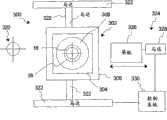
Fig. 1 is a synoptic diagram, and the lithographic press 10 with feature of the present invention is shown.This lithographic press 10 comprisessupport 12, illuminator 14 (irradiation unit),optical module 16,grating platform assembly 18,work stage assembly 20,measuring system 22,control system 24 and ambient fluid system 26.For adapting to the designing requirement of lithographic press 10, can change the design of lithographic press 10 parts.
In one embodiment, adopt this lithographic press 10, the integrated circuit patterns (not shown) on the grating (reticle) 28 is projected on the semiconductor wafer 30 (being shown in broken lines).This lithographic press 10 is contained on the mount pad 32, for example is contained on ground, base or floor or other the other supporting members.
In various embodiment of the present invention, can make the scan-type etching system with lithographic press 10, this system can make pattern exposure on thegrating 28 onwafer 30, and grating 28 andwafer 30 can same moved further.In a kind of scan-type lithographic press, this grating 28 utilizesgrating platform assembly 18, can do motion perpendicular tooptical module 16 optical axises, and wafer 30 utilizeswafer station assembly 20 can do motion perpendicular tooptical module 16 optical axises, during grating 28 andwafer 30 are with moved further, scan thisgrating 28 and wafer 30.
According to another kind of mode, lithographic press 10 can be a repetition step-by-step movement etching system, when grating 28 andwafer 30 are motionless, and this etching system exposure grating 28.In the formula of repetition stepping technology, when each zone of exposure,wafer 30 is positioned at constant position with respect to grating 28 and optical module 16.Therefore, during exposing operation step in succession, this wafer moves with the optical axis ofwafer station assembly 20 adjoining lands perpendicular tooptical module 16, makes next zone ofwafer 30 with respect tooptical module 16 and grating 28 fix in position, so that exposure.After this operation, image sequence ground on thegrating 28 exposes on the zone of wafer, and then next zone that makeswafer 30 is with respect tooptical module 16 and grating 28 fix in position.
Use lithographic press 10 provided herein not necessarily to be limited to and make semi-conductive etching system.For example, lithographic press 10 can be used as LCD (LCD) etching system, and this system on rectangular glass plate, perhaps is used as the etching system of making thin-film head with liquid crystal display workpiece pattern exposure.Therefore, used herein term " workpiece " is meant a kind of device, forms image with lithographic plate printing method on this device, for example forms pattern on wafer or LCD end liner, but is not limited to wafer and LCD.
The parts ofequipment supporter 12 bearing flat plate printing machines 10, theequipment supporter 12 that is shown in Fig. 1 supportsgrating platform assembly 18,wafer station assembly 20,optical module 16 and theilluminator 14 that is positioned at above the mounting seat 32.
Thislighting source 34 can be g spectral line light source (436nm), i spectral line light source (365nm), KrF laser (248nm), ArF laser (193nm) or F2Laser (157nm).According to another kind of mode,radiation source 34 can be launched X ray.
In addition, when adopting wavelength to be 200nm or littler vacuum ultraviolet line exposing workpiece, can consider to use anti-refractive optical system.The example of anti-refractive optical system comprises Japanese patent application No.8-171054 and its corresponding U.S. Patent No. 5668672 and Japanese patent application No.10-20195 and its corresponding U.S. Patent No. 5835275 of announcing in the publication application publication.In these cases, the catoptrics workpiece can be anti-refractive optical system, comprises beam splitter and concave mirror.The Japanese patent application No.8-334695 that on publication application bulletin, announces and its corresponding U.S. Patent No. 5689377 and Japanese patent application No.10-3039 and its corresponding U.S. Patent application No.873605 (date of application: on Dec 6th, 1997), also use reflected refraction formula optical system, this system comprises concave mirror etc., but do not have beam splitter, these patents all can be used for the present invention.The content of the Japanese patent application that distributes in allow, above-mentioned United States Patent (USP) and publication application are announced all is included in herein as a reference.
Eachmotion assembly corresponding platform motion assembly corresponding platform platform motion assembly 40 and workstage motion assembly 44 comprise one or more driver respectively, for example rotation motor, voice coil motor, utilize Luo Lunzili produce the linear motor, electromagnetic driver, planar motors of driving force or other other add power drive.
In etching system, in wafer station assembly or grating platform assembly, adopt linear motor (to see U.S. Patent No. 5623853 or 5528118, be included in herein as a reference) time, this linear motor can be a gas suspension motor of using air cushion, or utilizes the magnetic suspension motor of Luo Lunzili or magnetic reactance power.In addition, this can be moved along guide, perhaps this can be need not any guide no guide type platform.
According to another kind of mode, can drive a platform in these with planar motors, this planar motors utilization drives this by the electromagnetic force that permanent magnet unit and armature coil unit produce, this permanent magnet unit has the permanent magnet of bidimensional configuration, and this armature coil has the coil that is positioned at relative position of bidimensional configuration.When adopting this drive system, permanent magnet unit or armature coil unit are connected in the base of platform, and wherein another unit is contained on this motion side plane.
The motion of above-mentioned estrade produces reacting force, and this acting force may influence the operating performance of etching system.The reacting force that is produced by the motion of wafer (end liner) platform can be sent on the floor (floor) by mechanical effect by used bracket component, as described in the Japanese patent application No.8-136475 of U.S. Patent No. 5528100 and announcement.In addition, the reacting force that the motion of grating (mask) platform produces mechanically is sent on the floor (base plate) by the bracket component that uses, as U.S. Patent No. 8574820 and date of publication present patent application No.8-330224.Through permission, the content of U.S. Patent No. 5528100,5874820 and Japanese patent application No.8-330224 is included in herein as a reference.
Thiscontrol device 24 receives the information of measuringsystem 22, and themotion assembly control system 24 can be controlled the operation ofperipheral system 26 parts.Thiscontrol system 24 comprises one or more processor and circuit.
Theseperipheral system 26 controls environment in the gap betweenoptical module 16 and wafer 30.This gap comprises into image field.This one-tenth image field comprises in abutting connection withwafer 30 will the expose zone at position and the zone that the luminous energy light beam passes through betweenoptical module 16 and wafer 30.For this design,peripheral system 26 may be controlled to the environment in the image field.Can be according to the design ofwafer 30 and lithographic press remaining part, change is produced in the gap and/or the controllable environment that requires byperipheral system 26, and the parts of this lithographic press 10 comprise illuminator 14.For example, the controllable environment of requirement can be a for example water of fluid.According to another kind of mode, the controllable environment of requirement can be a for example gas of one other fluid.In various embodiments, the height of this gap between last optical module of the top surface ofwafer 30 andoptical module 16 is between 0.1-10mm.
In one embodiment, theseperipheral system 26 usefulness immersion fluids are full of into the remainder in image field and gap.Can change the design ofperipheral system 26 and theseperipheral system 26 parts.In different embodiment, theseperipheral system 26 usefulness nozzles, electronic sponge, porosint etc. are transported to immersion fluid and/or be injected in this gaps, and adopt vacuum pump, sponge etc. to remove fluid in this gap.Can change the design of peripheral system 26.For example, immersion fluid can inject in the gap or near one or more position in gap in this system.In addition, this immersion fluid system helps atworkpiece 30, this gap and/oroptical module 16 edges, perhaps removes and/or remove these immersion fluids near one of these parts and a plurality of positions.Further details for various peripheral systems, can be with reference to the U.S. Provisional Patent Application 60/462142 that is entitled as " immersion offset printing fluid control systems " that proposed on April 9th, 2003, the U.S. Provisional Application 60/462112 that is entitled as " the vacuum loop systems of immersion lithographic press and imbibition loop systems " that on April 10th, 2003 proposed, the U.S. Provisional Patent Application 60/541329 that is entitled as " immersion offset printing sprinkler design " that the U.S. Provisional Patent Application 60/500312 of " the noiselessness fluid recycling apparatus with porosint " that on September 3rd, 2003 proposed and on April 2nd, 2004 propose, all these patents all are included in herein as a reference.
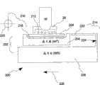
With reference to figure 2, the cross-sectional view of the lithographic press of one embodiment of the invention shown in the figure.Thislithographic press 200 comprisesoptical module 16 andplatform assembly 202, and this assembly compriseswafer holder 204 and wafer station 206.Thiswafer holder 204 do to become wafer 208 (the perhaps workpiece of any other type) can be bearing inoptical module 16 below.Carry immersion fluid 212 around the gap that theperipheral system 26 of thisoptical module 16 is used betweenwafer 208 andoptical module 16 last optics, and remove the immersion fluid in this gap.Workpiece is changedsystem 216 and is comprised wafer loading bin 218 (being mechanical arm) and alignment tool 220 (being micro-CCD camera), and this replacing system does to become and can take offwafer 208 fromwafer holder 204, and replaces this wafer with second wafer.Finish this operation and adoptwafer loading bin 218 usually, the wafer on thewafer holder 204 208 is raise, and take off this wafer.Subsequently the second wafer (not shown) is placed on thewafer chuck 218, and aims at, be positioned at then on thewafer holder 204 that is positioned at below theoptical module 16 withalignment tool 220.
Adopt this embodiment,wafer station 206 comprises immersion fluid constrainedsystem 214, and this system does to become, and canimmersion fluid 212 can be remained near in the gap ofoptical module 16 last optics during changing wafer.This immersion fluid constrainedsystem 214 comprises thebacking plate 222 near wafer holder 204.Thesupport unit 224 that employing is configured betweenbacking plate 222 and thewafer station 206 comes bearing plate 222.Thiswafer holder 204 has the upper flat surface, the surperficial copline of this surface and wafer 208.Thisbacking plate 222 also has the surface of upper flat, the upper surface of this surface andwafer holder 204 and wafer surface copline.Thisbacking plate 222 has very little gap (for example 0.1-1.00mm) therebetween nearwafer holder 204 configurations, makesimmersion fluid 212 to flow between wafer holder andbacking plate 222, and can seepage.During changing wafer,wafer station 206 moves along the direction ofarrow 226, makebacking plate 222 replacewafer station 204 be positioned atoptical module 16 below, thereby keep fluid in the gap, perhaps keep the size of this fluid gap.After aiming at new wafer, wafer station is moved to its original position backward, thereby when second wafer orientation was belowoptical module 16,backing plate 222 moved apart this gap.In various embodiments,backing plate 222 can be followedwafer station 204 configurations, does not form any gap betwixt.Can regulate the upright position and/or the degree of tilt ofwafer holder 204, make beforewafer station 204 shifts out belowoptical module 16, this wafer station surface and backing plate surface copline.The gap is not limited to above-mentioned replacing wafer operation betweenmaintenance backing plate 222 and the optical module 16.During alignment function or measuring operation,backing plate 222 can be even as big as remaining onimmersion fluid 212 in the space betweenbacking plate 222 and the optical module 16.In these operations, that part of zone that is occupied byimmersion fluid 212 is positioned on the upper surface ofwafer station 204.
With reference to figure 3A and 3B, the cross-sectional view and the top view of the another kind of immersion lithographic press of another embodiment of the present invention shown in the figure.Thislithographic press 300 comprisesoptical module 16 andplatform assembly 302, and this assembly compriseswafer holder 304 and wafer station 306.Thiswafer holder 304 do to become wafer 308 (the perhaps workpiece of any other type) can be bearing inoptical module 16 below.Immersion fluid 312 is carried in the gap that theperipheral system 26 of encirclementoptical module 16 is used betweenwafer 308 andoptical module 16 bottom opticses, and removes the immersion fluid in this gap.Workpiece is changed system 316 and is comprised wafer loading bin 318 andalignment tool 320, and this replacing system does to become and can take offwafer 308 fromwafer holder 304, and replaces this wafer with second wafer.Finish this operation and be and adopt the wafer loading bin thatwafer 308 is taken off from wafer holder.Subsequently, the second wafer (not shown) is contained on the wafer chuck 318, aims atalignment tool 320, be positioned at thenoptical module 16 below.Illustrate as Fig. 3 B is clear, during operation, adopt one group ofmotor 322 with two degree of freedom (X and Y)transfer table assembly 302, this assembly compriseswafer holder 304 and wafer station 306.As mentioned above, thismotor 322 can be the motor of any kind, for example, and rotation motor, linear motor, voice coil motor etc.
Immersionlithographic press 300 also comprises immersion fluid constrainedsystem 324, and this system does to become, and whenwafer holder 304 shifting out below optical module, immersion fluid 312 can be remained in the space below this optical module 16.This immersion fluid constrainedsystem 324 comprisesbacking plate 326,motor 328 and control system 330.Thisbacking plate 326 is in abutting connection withoptical module 16 andwafer station 204 configurations.Thiswafer holder 304 has the upper flat surface, the surperficial copline of this surface and wafer 308.Thisbacking plate 326 has the upper flat surface, the upper surface of this surface andwafer holder 304 and wafer surface copline.Thisbacking plate 326 can move at X and Y direction with motor 328.Thismotor 328 is bycontrol system 330controls.Motor 328 can be the motor and themotor 322 of any kind.When wafer holder 304 (wafer station 306) is removed belowoptical module 16,backing plate 326 just be positioned atoptical module 16 below.When replacing wafer,wafer holder 304 moves apart optical module 16.Simultaneously,control system 330 operatedmotors 328, withbacking plate 326 move on to optical module below, replace wafer holder 304.Thereforebacking plate 326 remains on immersion fluid 312 in the gap below the optical module 16.After aiming at new wafer withalignment tool 320, withwafer station 304 be repositioned atoptical module 16 below.At the same time,control system 330 operatedmotors 328 makebacking plate 326 return from the gap, overflow so that prevent immersion fluid 312.When wafer was changed operation,control system 330 movedwafer holder 304 andbacking plate 326, has little gap between thiswafer station 304 andbacking plate 326, and the immersion fluid 312 below the optical module flows betweenwafer holder 304 and backing plate 326.Therefore, immersion fluid constrainedsystem 324 can keep the immersion fluid 312 in the gap during replacing wafer.In this embodiment, wafer holder 304 (wafer station 306) andbacking plate 326 are independently movings.Therefore,wafer holder 304 can move freely, and immersion fluid 312 remains in the space betweenbacking plate 326 and the optical module 16.In various embodiment of the present invention,control system 330 can be independent control system, perhaps can also merge to the control system of themotor 322 that is used forpositions wafer platform 306 and wafer holder 304.Can regulate the upright position and/or the degree of tilt of at least one parts inwafer holder 304 and thebacking plate 326, make wafer holder surface and backing plate surface copline, and then wafer holder is shifted out below optical module 16.The operation of shifting outwafer holder 304 belowoptical module 16 not necessarily is limited to the wafer replacement operation.For example, in the time of in the space that immersion fluid is remained betweenbacking plate 326 and theoptical module 16, can carry out alignment procedure, measuring operation or other operations.
With reference to Fig. 4 A and 4B, two cross-sectional views of the lithographic press of immersion shown in the figure.Thislithographic press 400 comprisesoptical module 16 andplatform assembly 402, and this assembly compriseswafer holder 404 and wafer station 406.Thiswafer holder 404 do to become wafer 408 (the perhaps workpiece of any other type) can be bearing inoptical module 16 below.Immersion fluid 412 is carried in the gap that theexternal system 26 of surrounding thisoptical module 16 is used betweenwafer 408 and optical module foot optics, and is used for removing the immersion fluid in this gap.Workpiece is changedsystem 416 and is comprisedwafer loading bin 418 andalignment tool 420, and this replacing system does to become and can take offwafer 408 fromwafer holder 404, and replaces this wafer with second wafer.Finishing this operation is withwafer loading bin 418, takes offwafer 408 from wafer holder 404.Subsequently, the second wafer (not shown) is placed on thewafer chuck 418, withalignment tool 420 collimation, be positioned at thenoptical module 16 below, shown in Fig. 4 A.
Immersionlithographic press 400 also comprises immersion fluid constrainedsystem 424, and this system does to become, and whenwafer holder 404 shifts out belowoptical module 16,immersion fluid 412 is remained in the space below the optical module 16.This immersion fluid constrainedsystem 424 comprisesbacking plate 426, be formed onfirst anchor clamps 428 on theoptical module 16 and be formed onsecond anchor clamps 430 on the wafer holder 404.Whenimmersion fluid 412 remained betweenoptical module 16 and the wafer holder 404 (perhaps wafer 408), thisbacking plate 426 was fixed on position on thewafer holder 404 by second anchor clamps 430.For example changing wafer operating period when moving apartoptical module 16 whenwafer holder 404,backing plate 426 is just thrown off withwafer holder 404, and fixing byfirst anchor clamps 428, therebyimmersion fluid 412 is remained betweenoptical module 16 and the backing plate 426.Thiswafer holder 404 has flat upper surface, the surperficial copline of this surface and wafer 408.Thebacking plate 426 that is fixed on thewafer holder 404 also has the upper flat surface, the upper surface of this surface andwafer holder 404 and wafer surface copline.Therefore,backing plate 426 andwafer 408 can be moved on to optical module below, and the immersion fluid seepage does not take place.In various embodiments,anchor clamps
Illustrate as Fig. 4 A is clear,backing plate 426 is positioned on thewafer holder 404 when brilliant 408 expose.During wafer exposure, adoptsecond anchor clamps 430 to makebacking plate 426 be located in position on the wafer holder 404.During the replacement wafer shown in Fig. 4 B,wafer holder 404 is moved along the direction of arrow 432, make backing plate be positioned atoptical module 16 below, replace wafer 408.When carrying out this operation, second anchor clamps thatbacking plate 426 are fixed inwafer holder 404 unclamp, andfirst anchor clamps 428 are fixed inoptical module 16 with backing plate 426.As a result,immersion fluid 412 when changingwafer 408, can remain on optical module below.The collimation wafer after,wafer holder 404 is moved along the opposite direction of arrow 432, with new wafer orientation below optical module.Before this motion,first anchor clamps 428 unclamp, andsecond anchor clamps 430 are fixed inwafer holder 404 withbacking plate 426 again.In this embodiment, byfirst anchor clamps 428 fixedly the time,wafer holder 404 can move freely atbacking plate 426.
In various embodiments, byfirst anchor clamps 428 fixedly the operation ofbacking plate 426 be not limited only to the wafer replacement operation.When immersion fluid 312 remains on the space that forms between thefixing backing plate 426 ofoptical module 16 andfirst anchor clamps 428, the operation that can also collimate, measuring operation or any other operation.In addition,anchor clamps 428 are configured onsupport 12 or other support units, andanchor clamps 430 are configured on the wafer station 406.Backing plate 426 can remain on the movable part except thatplatform assembly 420.
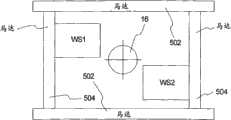
Fig. 5 A and 5B are top views, and the two desk-top submergence lithography system of two differences of other embodiments of the invention are shown.For the basic structure and the operation of this two desk-top submergence lithography system, please referring to U.S. Patent No. 6262796 and 6341007.Through allowing, this U.S. Patent No. 6262796 and 6341007 content are included in herein as a reference.In two embodiment, a pair of wafer station WS1 and WS2 are shown.Usemotor 502 and move in the horizontal direction or locate two platform WS1 and WS2, and move and locate WS1 and WS2 in vertical direction with motor 504.Adoptmotor optical module 16 below, on another platform, carry out wafer simultaneously and change and alignment procedure.After wafer belowoptical module 16 is finished exposure, make two estrade exchanges, and repeat aforesaid operations.For any structure wherein, can be used for wherein any pair desktop apparatus with reference to the described various embodiment of Fig. 2-4 with above of the present invention, immersion fluid is remained in the gap below the optical module 16.For embodiment for example shown in Figure 2, can change each wafer station WS1 and the WS2 shown in Fig. 5 A or the 5B, change over and comprisebacking plate 222 and support unit 224.And, can adoptsingle backing plate 326,motor 328 andcontrol system 330 nearoptical module 16 for embodiment shown in Figure 3.Thisbacking plate 326 can move apart platform WS1 and WS2 individually.Between wafer station WS1 and WS2 commutation period,backing plate 326 can be moved on tooptical module 16 below so that with immersion fluid 312 remain onoptical module 16 below.Last for embodiment shown in Figure 4, can adopt the single backing plate that can throw off.When wafer station WS1 and WS2 exchange, can usebacking plate 426 immersion fluid is remained in the gap shown in Fig. 4 B.On the other hand, between exposure period, backing plate can be fixed on the wafer holder of the wafer station of just exposing.In this manner, two wafer station WS1 and WS2 only need a backing plate.According to another kind of mode, as described below, also can make backing plate with second.
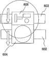
With reference to figure 6A, implement the two desk-top lithographic press of one embodiment of the invention shown in the figure.In this embodiment,immersion lithography system 600 comprises first 604 and second 606.These two platforms can drive bymotor 602 and move at X and Y direction.In this embodiment, canapplication station optical module 16 below, in the time will replacing workpiece, second 606 of second workpiece is housed withmotor 602 location, make it in abutting connection with first 604.For and two platforms of row arrangement, they form continuous surface basically.Then, usemotor 602 and as one man move these two platforms, make be positioned at for second 606optical module 16 below, and first no longer be positioned atoptical module 16 below, utilize second 606 immersion fluid that keeps in the gap, this second with first surface that formation is continuous basically.In various other embodiment, second 606 also can be " the backing plate platform " that backing plate is housed, and when second workpiece is placed on first 604, can immersion fluid be remained in the gap with this backing plate platform.Equally, can adopt the motor apparatus shown in Fig. 5 A or the 5B.
Fig. 6 B-6E is a series of synoptic diagram, and the workpiece that one embodiment of the invention is shown is changed.After Fig. 6 B is illustrated in and finishes exposure, be positioned at the wafer on the platform 604.Fig. 6 C illustrates belowoptical module 16 first 604 and contacts (perhaps near) second 606.Fig. 6 D illustrates the transfer of generation, be about to second 606 be positioned atoptical module 16 below.In Fig. 6 E, first 604 has moved apartoptical module 16 at last.Illustrate as Fig. 6 C and 6D are clear, these twoplatforms optical module 16, therefore immersion fluid can be remained in the gap.In the illustrated embodiment, second 606 is backing plate platforms.Yet this also can be aforesaid work stage.
In above-mentioned various embodiment, this backing plate can be with many different made, for example stupalith, metal material, plastics.These materials can be coated with one deck teflon according to other embodiment.The size of backing plate also should be fully big, so that cover the zone that is occupied by immersion fluid.In above-mentioned various embodiment, the total surface ofoptical module 16 last optics is to be under the state of immersion fluid environment, thereby can prevent the formation (for example " water spots ") of fluid spot.
When adopting said system, can utilize total technology that is shown in Fig. 7 A to makesemiconductor wafer.In step 701, the function and the operating performance of design workpiece.Then instep 702, have the mask (grating) of pattern according to previous design procedure design, and instep 703 arranged side by side, make wafer withsilicon materials.In step 704, adopt on the wafer of etching system with mask pattern exposure formation instep 703 ofstep 702 design of the invention described above.Instep 705, assembled semiconductor wafer (comprising cutting operation, welding operation and packaging operation), this workpiece of check instep 706 at last.
Fig. 7 B is illustrated in when making semiconductor workpiece, and detailed process flow diagram illustrates the details of above-mentioned steps 704.In the step 711 (oxidation step) of Fig. 7 B, the oxidation wafer surface.In step 712 (CVD step), on wafer surface, form dielectric film.In step 713 (electrode formation step), on wafer, form electrode with vapor deposition process.In step 714 (ion implantation step), ion is injected in the wafer.Above-mentioned steps 711-714 handles during the wafer pre-treatment step of wafer.Can select each step according to processing requirements.
After finishing above-mentioned pre-treatment step, on each platform of processing of wafers, finish following post-processing step.During aftertreatment, at first in step 715 (photoresist formation step), photoresist is coated on the wafer, in step 716 (step of exposure), the above-mentioned workpiece that exposes is transferred to mask (grating) circuit pattern on the wafer then.In step 717 (development step), the wafer that develops and exposed in step 718 (corrosion step), is removed the part that is not residue photoresist (material surface that has exposed) with caustic solution.In step 719 (photoresist is removed step), the unwanted photoresist that stays after the corrosion is removed.
Repeat these pre-service and post-processing step and can form a plurality of circuit patterns.
Although above-mentioned disclosed special lithographic press can meet the requirements of purpose fully and obtain above-mentioned advantage, but be understood that, these concrete printing machines only example illustrate the present preferred embodiment of the present invention, and can not limit claims structure shown in this article or design details in addition.
Claims (40)
1. submergence exposure sources with the light beam exposure base comprises:
Optical module, described light beam sees through described optical module and shines on the described substrate;
Substrate holder, described substrate holder support described substrate and can move relative to described optical module; And
The backing plate assembly, described backing plate assembly can move relative to described substrate holder,
Wherein said substrate holder and described backing plate assembly move during from first state-transition to second state together, described first state is meant that immersion fluid maintains in the space between described optical module and the described substrate holder, described second state is meant that described immersion fluid maintains in the space between described optical module and the described backing plate assembly, and described optical module kept contacting with described immersion fluid between tour.
2. submergence exposure sources as claimed in claim 1, wherein said substrate holder and described backing plate assembly move with quite approaching each other configuration status, cause described immersion fluid to maintain in fact and are located immediately in the space of described optical module below.
3. submergence exposure sources as claimed in claim 2, wherein said substrate holder and described backing plate assembly move in fact simultaneously.
4. submergence exposure sources as claimed in claim 2, wherein when keeping described first state, described substrate and described backing plate assembly relatively move toward each other, cause the quite closely configuration each other of described substrate holder and described backing plate assembly.
5. submergence exposure sources as claimed in claim 1, wherein said backing plate assembly replaces described substrate holder and locatees opposite to each other with described optical module, with when described substrate holder is mobile away from described optical module below, keep in fact in the space of described immersion fluid below described optical module.
6. submergence exposure sources as claimed in claim 1, wherein before described substrate holder moved below away from described optical module, described substrate holder and described backing plate assembly relatively tilted and/or move in vertical direction.
7. submergence exposure sources as claimed in claim 1, wherein said backing plate assembly comprises the microscope carrier different with described substrate holder.
8. submergence exposure sources as claimed in claim 1, wherein between the exposure period of the described substrate that is supported by described substrate holder, described backing plate assembly is away from location, ground, described optical module below.
9. submergence exposure sources as claimed in claim 1, wherein between described tour, described substrate holder and described backing plate assembly form continuous in fact surface.
10. submergence exposure sources as claimed in claim 1 further comprises: substrate is changed system, and described substrate is changed system configuration and become to change the substrate that is on the described substrate holder in described second state.
11. submergence exposure sources as claimed in claim 10 further comprises: colimated light system, described colimated light system is configured to carry out the collimation that is supported on the substrate on the described substrate holder by replacing.
12. the submergence exposure sources with the light beam exposure base comprises:
Optical module, described light beam sees through described optical module and shines on the described substrate;
First microscope carrier, described first microscope carrier support described substrate and can move relative to described optical module; And
Second microscope carrier, described second microscope carrier can move relative to described first microscope carrier,
Wherein said first microscope carrier and described second microscope carrier move during from first state-transition to second state together, described first state is meant that immersion fluid maintains in the space between the microscope carrier in described optical module and described first microscope carrier and described second microscope carrier, described second state is meant that described immersion fluid maintains in the space between another microscope carrier in described optical module and described first microscope carrier and described second microscope carrier, and described optical module kept contacting with described immersion fluid between tour.
13. submergence exposure sources as claimed in claim 12, wherein said first microscope carrier and described second microscope carrier move with quite approaching each other configuration status, cause described immersion fluid to maintain in fact and are located immediately in the space of described optical module below.
14. submergence exposure sources as claimed in claim 13, wherein said first microscope carrier and described second microscope carrier move in fact simultaneously.
15. submergence exposure sources as claimed in claim 13, wherein when keeping described first state, described first microscope carrier and described second microscope carrier relatively move toward each other, cause the quite closely configuration each other of described first microscope carrier and described second microscope carrier.
16. submergence exposure sources as claimed in claim 12, wherein said second microscope carrier replaces described first microscope carrier and locatees opposite to each other with described optical module, with when described first microscope carrier is mobile away from ground, described optical module below, keep in fact in the space of described immersion fluid below described optical module.
17. submergence exposure sources as claimed in claim 12, wherein before described first microscope carrier moved below away from described optical module, described first microscope carrier and described second microscope carrier relatively tilted and/or move in vertical direction.
18. submergence exposure sources as claimed in claim 12, wherein between the exposure period of the described substrate that is supported by described first microscope carrier, described second microscope carrier is away from location, ground, described optical module below.
19. submergence exposure sources as claimed in claim 12 further comprises: substrate is changed system, and described substrate is changed system configuration and become to change the substrate that is on described first microscope carrier in described second state.
20. submergence exposure sources as claimed in claim 19 further comprises: colimated light system, described colimated light system are configured to carry out the collimation that is supported on the substrate on described first microscope carrier by replacing.
21. the submergence exposure method with the light beam exposure base comprises the steps:
Described substrate is placed on the substrate holder;
See through optical module and immersion fluid with described light beam irradiates to the described substrate that is positioned on the described substrate holder; And
When keeping contacting between described optical module and the described immersion fluid, with described substrate holder and backing plate assembly along moving each other, so that become second state from first state-transition, described substrate holder and described backing plate assembly can relatively move, described first state is meant that described immersion fluid maintains in the space between described optical module and the described substrate holder, and described second state is meant that described immersion fluid maintains in the space between described optical module and the described backing plate assembly.
22. submergence exposure method as claimed in claim 21, wherein said substrate holder and described backing plate assembly move with quite approaching each other configuration status, cause described immersion fluid to maintain in fact and are located immediately in the space of described optical module below.
23. submergence exposure method as claimed in claim 22, wherein said substrate holder and described backing plate assembly move in fact simultaneously.
24. submergence exposure method as claimed in claim 22, wherein when keeping described first state, described substrate and described backing plate assembly relatively move toward each other, cause the quite closely configuration each other of described substrate holder and described backing plate assembly.
25. submergence exposure method as claimed in claim 21, wherein said backing plate assembly replaces described substrate holder and locatees opposite to each other with described optical module, with when described substrate holder is mobile away from ground, described optical module below, keep in fact in the space of described immersion fluid below described optical module.
26. submergence exposure method as claimed in claim 21, wherein before described substrate holder moved below away from described optical module, described substrate holder and described backing plate assembly relatively tilted and/or move in vertical direction.
27. submergence exposure method as claimed in claim 21, wherein said backing plate assembly comprises the microscope carrier different with described substrate holder.
28. submergence exposure method as claimed in claim 21, wherein between the exposure period of the described substrate that is supported by described substrate holder, described backing plate assembly is away from location, ground, described optical module below.
29. submergence exposure method as claimed in claim 21, wherein between described tour, described substrate holder and described backing plate assembly form continuous in fact surface.
30. submergence exposure method as claimed in claim 21 comprises the steps: that further placement substrate replacing system is to change the substrate that is on the described substrate holder in described second state.
31. submergence exposure method as claimed in claim 30 further comprises the steps: to dispose colimated light system to carry out the collimation that is supported on the substrate on the described substrate holder by replacing.
32. the submergence exposure method with the light beam exposure base comprises the steps:
Described substrate is placed on first microscope carrier;
See through optical module and immersion fluid with described light beam irradiates to the described substrate that is positioned on described first microscope carrier; And
When keeping contacting between described optical module and the described immersion fluid, with described first microscope carrier and second microscope carrier along moving each other, so that become second state from first state-transition, described first microscope carrier and described second microscope carrier can relatively move, described first state is meant that described immersion fluid maintains in the space between the microscope carrier in described optical module and described first microscope carrier and described second microscope carrier, and described second state is meant that described immersion fluid maintains in the space between another microscope carrier in described optical module and described first microscope carrier and described second microscope carrier.
33. submergence exposure method as claimed in claim 32, wherein said first microscope carrier and described second microscope carrier move with quite approaching each other configuration status, cause described immersion fluid to maintain in fact and are located immediately in the space of described optical module below.
34. submergence exposure method as claimed in claim 33, wherein said first microscope carrier and described second microscope carrier move in fact simultaneously.
35. submergence exposure method as claimed in claim 33, wherein when keeping described first state, described first microscope carrier and described second microscope carrier relatively move toward each other, cause the quite closely configuration each other of described first microscope carrier and described second microscope carrier.
36. submergence exposure method as claimed in claim 32, wherein said second microscope carrier replaces described first microscope carrier and locatees opposite to each other with described optical module, with when described first microscope carrier is mobile away from ground, described optical module below, keep in fact in the space of described immersion fluid below described optical module.
37. submergence exposure method as claimed in claim 32, wherein before described first microscope carrier moved below away from described optical module, described first microscope carrier and described second microscope carrier relatively tilted and/or move in vertical direction.
38. submergence exposure method as claimed in claim 32, wherein between the exposure period of the described substrate that is supported by described first microscope carrier, described second microscope carrier is away from location, ground, described optical module below.
39. submergence exposure method as claimed in claim 32 comprises the steps: that further placement substrate replacing system is to change the substrate that is on described first microscope carrier in described second state.
40. submergence exposure method as claimed in claim 39 further comprises the steps: to dispose colimated light system to carry out the collimation that is supported on the substrate on described first microscope carrier by replacing.
Applications Claiming Priority (2)
| Application Number | Priority Date | Filing Date | Title |
|---|---|---|---|
| US46249903P | 2003-04-11 | 2003-04-11 | |
| US60/462,499 | 2003-04-11 |
Related Parent Applications (1)
| Application Number | Title | Priority Date | Filing Date |
|---|---|---|---|
| CN2004800097020ADivisionCN101002140B (en) | 2003-04-11 | 2004-03-17 | Apparatus and method for maintaining immersion fluid under a lithographic projection lens |
Publications (2)
| Publication Number | Publication Date |
|---|---|
| CN101980086Atrue CN101980086A (en) | 2011-02-23 |
| CN101980086B CN101980086B (en) | 2014-01-01 |
Family
ID=33159850
Family Applications (3)
| Application Number | Title | Priority Date | Filing Date |
|---|---|---|---|
| CN201010510290.6AExpired - LifetimeCN101980086B (en) | 2003-04-11 | 2004-03-17 | Immersion exposure apparatus and method |
| CN2010105103063AExpired - LifetimeCN101980087B (en) | 2003-04-11 | 2004-03-17 | Immersion exposure appratus and method |
| CN2004800097020AExpired - LifetimeCN101002140B (en) | 2003-04-11 | 2004-03-17 | Apparatus and method for maintaining immersion fluid under a lithographic projection lens |
Family Applications After (2)
| Application Number | Title | Priority Date | Filing Date |
|---|---|---|---|
| CN2010105103063AExpired - LifetimeCN101980087B (en) | 2003-04-11 | 2004-03-17 | Immersion exposure appratus and method |
| CN2004800097020AExpired - LifetimeCN101002140B (en) | 2003-04-11 | 2004-03-17 | Apparatus and method for maintaining immersion fluid under a lithographic projection lens |
Country Status (9)
| Country | Link |
|---|---|
| US (18) | US7372538B2 (en) |
| EP (8) | EP3141953A3 (en) |
| JP (12) | JP4315198B2 (en) |
| KR (15) | KR101225884B1 (en) |
| CN (3) | CN101980086B (en) |
| IL (5) | IL170735A (en) |
| SG (12) | SG139734A1 (en) |
| TW (16) | TWI545387B (en) |
| WO (1) | WO2004090577A2 (en) |
Families Citing this family (222)
| Publication number | Priority date | Publication date | Assignee | Title |
|---|---|---|---|---|
| EP1420299B1 (en) | 2002-11-12 | 2011-01-05 | ASML Netherlands B.V. | Immersion lithographic apparatus and device manufacturing method |
| US10503084B2 (en) | 2002-11-12 | 2019-12-10 | Asml Netherlands B.V. | Lithographic apparatus and device manufacturing method |
| US7372541B2 (en) | 2002-11-12 | 2008-05-13 | Asml Netherlands B.V. | Lithographic apparatus and device manufacturing method |
| DE60335595D1 (en) | 2002-11-12 | 2011-02-17 | Asml Netherlands Bv | Immersion lithographic apparatus and method of making a device |
| CN100568101C (en) | 2002-11-12 | 2009-12-09 | Asml荷兰有限公司 | Photolithography apparatus and device manufacturing method |
| US7110081B2 (en) | 2002-11-12 | 2006-09-19 | Asml Netherlands B.V. | Lithographic apparatus and device manufacturing method |
| KR100585476B1 (en) | 2002-11-12 | 2006-06-07 | 에이에스엠엘 네델란즈 비.브이. | Lithographic Apparatus and Device Manufacturing Method |
| US9482966B2 (en) | 2002-11-12 | 2016-11-01 | Asml Netherlands B.V. | Lithographic apparatus and device manufacturing method |
| SG121822A1 (en)* | 2002-11-12 | 2006-05-26 | Asml Netherlands Bv | Lithographic apparatus and device manufacturing method |
| KR101101737B1 (en) | 2002-12-10 | 2012-01-05 | 가부시키가이샤 니콘 | Exposure apparatus, exposure method and method for manufacturing device |
| US7948604B2 (en) | 2002-12-10 | 2011-05-24 | Nikon Corporation | Exposure apparatus and method for producing device |
| EP1571694A4 (en) | 2002-12-10 | 2008-10-15 | Nikon Corp | Exposure apparatus and method for manufacturing device |
| US7242455B2 (en) | 2002-12-10 | 2007-07-10 | Nikon Corporation | Exposure apparatus and method for producing device |
| KR20120127755A (en) | 2002-12-10 | 2012-11-23 | 가부시키가이샤 니콘 | Exposure apparatus and method for manufacturing device |
| WO2004053955A1 (en) | 2002-12-10 | 2004-06-24 | Nikon Corporation | Exposure system and device producing method |
| JP4352874B2 (en) | 2002-12-10 | 2009-10-28 | 株式会社ニコン | Exposure apparatus and device manufacturing method |
| DE10261775A1 (en) | 2002-12-20 | 2004-07-01 | Carl Zeiss Smt Ag | Device for the optical measurement of an imaging system |
| EP2466623B1 (en) | 2003-02-26 | 2015-04-22 | Nikon Corporation | Exposure apparatus, exposure method, and method for producing device |
| KR20050110033A (en) | 2003-03-25 | 2005-11-22 | 가부시키가이샤 니콘 | Exposure system and device production method |
| EP1612850B1 (en) | 2003-04-07 | 2009-03-25 | Nikon Corporation | Exposure apparatus and method for manufacturing a device |
| WO2004093159A2 (en) | 2003-04-09 | 2004-10-28 | Nikon Corporation | Immersion lithography fluid control system |
| EP2950147B1 (en) | 2003-04-10 | 2017-04-26 | Nikon Corporation | Environmental system including vaccum scavenge for an immersion lithography apparatus |
| EP3062152B1 (en) | 2003-04-10 | 2017-12-20 | Nikon Corporation | Environmental system including vaccum scavenge for an immersion lithography apparatus |
| EP3352010A1 (en) | 2003-04-10 | 2018-07-25 | Nikon Corporation | Run-off path to collect liquid for an immersion lithography apparatus |
| KR101225884B1 (en)* | 2003-04-11 | 2013-01-28 | 가부시키가이샤 니콘 | Apparatus and method for maintaining immersion fluid in the gap under the projection lens during wafer exchange in an immersion lithography machine |
| CN101825847B (en) | 2003-04-11 | 2013-10-16 | 株式会社尼康 | Cleanup method for optics in immersion lithography |
| JP4582089B2 (en) | 2003-04-11 | 2010-11-17 | 株式会社ニコン | Liquid jet recovery system for immersion lithography |
| SG194246A1 (en) | 2003-04-17 | 2013-11-29 | Nikon Corp | Optical arrangement of autofocus elements for use with immersion lithography |
| TWI295414B (en) | 2003-05-13 | 2008-04-01 | Asml Netherlands Bv | Lithographic apparatus and device manufacturing method |
| KR20060009356A (en) | 2003-05-15 | 2006-01-31 | 가부시키가이샤 니콘 | Exposure apparatus and device manufacturing method |
| TW201806001A (en) | 2003-05-23 | 2018-02-16 | 尼康股份有限公司 | Exposure device and device manufacturing method |
| TWI421906B (en) | 2003-05-23 | 2014-01-01 | 尼康股份有限公司 | An exposure method, an exposure apparatus, and an element manufacturing method |
| KR101548832B1 (en) | 2003-05-28 | 2015-09-01 | 가부시키가이샤 니콘 | Exposure method, exposure device, and device manufacturing method |
| US7213963B2 (en) | 2003-06-09 | 2007-05-08 | Asml Netherlands B.V. | Lithographic apparatus and device manufacturing method |
| EP2261741A3 (en) | 2003-06-11 | 2011-05-25 | ASML Netherlands B.V. | Lithographic apparatus and device manufacturing method |
| US7317504B2 (en) | 2004-04-08 | 2008-01-08 | Asml Netherlands B.V. | Lithographic apparatus and device manufacturing method |
| KR101242815B1 (en) | 2003-06-13 | 2013-03-12 | 가부시키가이샤 니콘 | Exposure method, substrate stage, exposure apparatus and method for manufacturing device |
| US6867844B2 (en) | 2003-06-19 | 2005-03-15 | Asml Holding N.V. | Immersion photolithography system and method using microchannel nozzles |
| TW201721717A (en) | 2003-06-19 | 2017-06-16 | 尼康股份有限公司 | Exposure apparatus, exposure method, and device manufacturing method |
| JP3862678B2 (en) | 2003-06-27 | 2006-12-27 | キヤノン株式会社 | Exposure apparatus and device manufacturing method |
| US6809794B1 (en) | 2003-06-27 | 2004-10-26 | Asml Holding N.V. | Immersion photolithography system and method using inverted wafer-projection optics interface |
| EP1491956B1 (en) | 2003-06-27 | 2006-09-06 | ASML Netherlands B.V. | Lithographic apparatus and device manufacturing method |
| KR20060027832A (en) | 2003-07-01 | 2006-03-28 | 가부시키가이샤 니콘 | Method of Using Isotopically Specified Fluids as Optical Elements |
| EP3179309A1 (en) | 2003-07-08 | 2017-06-14 | Nikon Corporation | Wafer table for immersion lithography |
| EP1643543B1 (en) | 2003-07-09 | 2010-11-24 | Nikon Corporation | Exposure apparatus and method for manufacturing device |
| WO2005006415A1 (en) | 2003-07-09 | 2005-01-20 | Nikon Corporation | Exposure apparatus and method for manufacturing device |
| WO2005006418A1 (en) | 2003-07-09 | 2005-01-20 | Nikon Corporation | Exposure apparatus and method for manufacturing device |
| WO2005010960A1 (en) | 2003-07-25 | 2005-02-03 | Nikon Corporation | Inspection method and inspection device for projection optical system, and production method for projection optical system |
| EP1503244A1 (en) | 2003-07-28 | 2005-02-02 | ASML Netherlands B.V. | Lithographic projection apparatus and device manufacturing method |
| KR101641011B1 (en) | 2003-07-28 | 2016-07-19 | 가부시키가이샤 니콘 | Exposure apparatus, device producing method, and exposure apparatus controlling method |
| US7175968B2 (en) | 2003-07-28 | 2007-02-13 | Asml Netherlands B.V. | Lithographic apparatus, device manufacturing method and a substrate |
| US7326522B2 (en) | 2004-02-11 | 2008-02-05 | Asml Netherlands B.V. | Device manufacturing method and a substrate |
| US7779781B2 (en) | 2003-07-31 | 2010-08-24 | Asml Netherlands B.V. | Lithographic apparatus and device manufacturing method |
| TWI263859B (en) | 2003-08-29 | 2006-10-11 | Asml Netherlands Bv | Lithographic apparatus and device manufacturing method |
| KR101380989B1 (en) | 2003-08-29 | 2014-04-04 | 가부시키가이샤 니콘 | Exposure apparatus and device producing method |
| EP3223053A1 (en) | 2003-09-03 | 2017-09-27 | Nikon Corporation | Apparatus and method for providing fluid for immersion lithography |
| JP4444920B2 (en) | 2003-09-19 | 2010-03-31 | 株式会社ニコン | Exposure apparatus and device manufacturing method |
| EP2837969B1 (en) | 2003-09-29 | 2016-04-20 | Nikon Corporation | Exposure apparatus, exposure method, and method for producing device |
| JP2005136364A (en) | 2003-10-08 | 2005-05-26 | Zao Nikon Co Ltd | Substrate transport apparatus, exposure apparatus, and device manufacturing method |
| KR101203028B1 (en) | 2003-10-08 | 2012-11-21 | 가부시키가이샤 자오 니콘 | Substrate carrying apparatus, substrate carrying method, exposure apparatus, exposure method, and method for producing device |
| KR20060126949A (en) | 2003-10-08 | 2006-12-11 | 가부시키가이샤 니콘 | Substrate conveyance apparatus and substrate conveyance method, exposure apparatus, exposure method, and device manufacturing method |
| TWI553701B (en) | 2003-10-09 | 2016-10-11 | 尼康股份有限公司 | Exposure apparatus and exposure method, component manufacturing method |
| US7411653B2 (en) | 2003-10-28 | 2008-08-12 | Asml Netherlands B.V. | Lithographic apparatus |
| US7352433B2 (en) | 2003-10-28 | 2008-04-01 | Asml Netherlands B.V. | Lithographic apparatus and device manufacturing method |
| US7528929B2 (en) | 2003-11-14 | 2009-05-05 | Asml Netherlands B.V. | Lithographic apparatus and device manufacturing method |
| KR101394764B1 (en)* | 2003-12-03 | 2014-05-27 | 가부시키가이샤 니콘 | Exposure apparatus, exposure method, device producing method, and optical component |
| JP4720506B2 (en) | 2003-12-15 | 2011-07-13 | 株式会社ニコン | Stage apparatus, exposure apparatus, and exposure method |
| US7394521B2 (en) | 2003-12-23 | 2008-07-01 | Asml Netherlands B.V. | Lithographic apparatus and device manufacturing method |
| DE602005019689D1 (en) | 2004-01-20 | 2010-04-15 | Zeiss Carl Smt Ag | EXPOSURE DEVICE AND MEASURING DEVICE FOR A PROJECTION SECTOR |
| US7589822B2 (en) | 2004-02-02 | 2009-09-15 | Nikon Corporation | Stage drive method and stage unit, exposure apparatus, and device manufacturing method |
| WO2005076321A1 (en) | 2004-02-03 | 2005-08-18 | Nikon Corporation | Exposure apparatus and method of producing device |
| KR101851511B1 (en) | 2004-03-25 | 2018-04-23 | 가부시키가이샤 니콘 | Exposure apparatus and method for manufacturing device |
| US7034917B2 (en) | 2004-04-01 | 2006-04-25 | Asml Netherlands B.V. | Lithographic apparatus, device manufacturing method and device manufactured thereby |
| US7898642B2 (en) | 2004-04-14 | 2011-03-01 | Asml Netherlands B.V. | Lithographic apparatus and device manufacturing method |
| US7400460B2 (en)* | 2004-04-26 | 2008-07-15 | Carl Zeiss Smt Ag | Method for connection of an optical element to a mount structure |
| US8054448B2 (en) | 2004-05-04 | 2011-11-08 | Nikon Corporation | Apparatus and method for providing fluid for immersion lithography |
| US7616383B2 (en) | 2004-05-18 | 2009-11-10 | Asml Netherlands B.V. | Lithographic apparatus and device manufacturing method |
| CN100594430C (en) | 2004-06-04 | 2010-03-17 | 卡尔蔡司Smt股份公司 | System for measuring image quality of optical imaging system |
| EP3203498A1 (en) | 2004-06-09 | 2017-08-09 | Nikon Corporation | Exposure apparatus and device manufacturing method |
| KR101227290B1 (en) | 2004-06-09 | 2013-01-29 | 가부시키가이샤 니콘 | Substrate holding device, exposure apparatus having same, exposure method, method for producing device, and liquid repellent plate |
| US7463330B2 (en) | 2004-07-07 | 2008-12-09 | Asml Netherlands B.V. | Lithographic apparatus and device manufacturing method |
| JP4894515B2 (en) | 2004-07-12 | 2012-03-14 | 株式会社ニコン | Exposure apparatus, device manufacturing method, and liquid detection method |
| US8169591B2 (en)* | 2004-08-03 | 2012-05-01 | Nikon Corporation | Exposure apparatus, exposure method, and method for producing device |
| TW200615716A (en)* | 2004-08-05 | 2006-05-16 | Nikon Corp | Stage device and exposure device |
| KR20070048164A (en) | 2004-08-18 | 2007-05-08 | 가부시키가이샤 니콘 | Exposure apparatus and device manufacturing method |
| US7701550B2 (en) | 2004-08-19 | 2010-04-20 | Asml Netherlands B.V. | Lithographic apparatus and device manufacturing method |
| KR101364347B1 (en)* | 2004-10-15 | 2014-02-18 | 가부시키가이샤 니콘 | Exposure apparatus and device manufacturing method |
| US7119876B2 (en) | 2004-10-18 | 2006-10-10 | Asml Netherlands B.V. | Lithographic apparatus and device manufacturing method |
| CN101598903A (en)* | 2004-11-01 | 2009-12-09 | 株式会社尼康 | Exposure device and exposure method |
| JP4517354B2 (en)* | 2004-11-08 | 2010-08-04 | 株式会社ニコン | Exposure apparatus and device manufacturing method |
| US7583357B2 (en)* | 2004-11-12 | 2009-09-01 | Asml Netherlands B.V. | Lithographic apparatus and device manufacturing method |
| US7411657B2 (en) | 2004-11-17 | 2008-08-12 | Asml Netherlands B.V. | Lithographic apparatus and device manufacturing method |
| TWI588872B (en)* | 2004-11-18 | 2017-06-21 | 尼康股份有限公司 | Position measurement method, position control method, measurement method, loading method, exposure method and exposure apparatus, and device manufacturing method |
| JP4807629B2 (en)* | 2004-11-25 | 2011-11-02 | 株式会社ニコン | Exposure apparatus and device manufacturing method |
| US7446850B2 (en) | 2004-12-03 | 2008-11-04 | Asml Netherlands B.V. | Lithographic apparatus and device manufacturing method |
| JP4784513B2 (en) | 2004-12-06 | 2011-10-05 | 株式会社ニコン | Maintenance method, maintenance equipment, exposure apparatus, and device manufacturing method |
| US7196770B2 (en) | 2004-12-07 | 2007-03-27 | Asml Netherlands B.V. | Prewetting of substrate before immersion exposure |
| US7397533B2 (en) | 2004-12-07 | 2008-07-08 | Asml Netherlands B.V. | Lithographic apparatus and device manufacturing method |
| US7365827B2 (en) | 2004-12-08 | 2008-04-29 | Asml Netherlands B.V. | Lithographic apparatus and device manufacturing method |
| JP4752473B2 (en) | 2004-12-09 | 2011-08-17 | 株式会社ニコン | Exposure apparatus, exposure method, and device manufacturing method |
| US7352440B2 (en) | 2004-12-10 | 2008-04-01 | Asml Netherlands B.V. | Substrate placement in immersion lithography |
| US7403261B2 (en) | 2004-12-15 | 2008-07-22 | Asml Netherlands B.V. | Lithographic apparatus and device manufacturing method |
| US7528931B2 (en) | 2004-12-20 | 2009-05-05 | Asml Netherlands B.V. | Lithographic apparatus and device manufacturing method |
| US7880860B2 (en) | 2004-12-20 | 2011-02-01 | Asml Netherlands B.V. | Lithographic apparatus and device manufacturing method |
| US7405805B2 (en) | 2004-12-28 | 2008-07-29 | Asml Netherlands B.V. | Lithographic apparatus and device manufacturing method |
| US7491661B2 (en) | 2004-12-28 | 2009-02-17 | Asml Netherlands B.V. | Device manufacturing method, top coat material and substrate |
| US20060147821A1 (en) | 2004-12-30 | 2006-07-06 | Asml Netherlands B.V. | Lithographic apparatus and device manufacturing method |
| DE602006012746D1 (en) | 2005-01-14 | 2010-04-22 | Asml Netherlands Bv | Lithographic apparatus and manufacturing method |
| US8692973B2 (en) | 2005-01-31 | 2014-04-08 | Nikon Corporation | Exposure apparatus and method for producing device |
| KR101513840B1 (en) | 2005-01-31 | 2015-04-20 | 가부시키가이샤 니콘 | Exposure apparatus and method for manufacturing device |
| CN102360170B (en) | 2005-02-10 | 2014-03-12 | Asml荷兰有限公司 | Immersion liquid, exposure apparatus, and exposure process |
| US8018573B2 (en) | 2005-02-22 | 2011-09-13 | Asml Netherlands B.V. | Lithographic apparatus and device manufacturing method |
| US7224431B2 (en) | 2005-02-22 | 2007-05-29 | Asml Netherlands B.V. | Lithographic apparatus and device manufacturing method |
| US7378025B2 (en) | 2005-02-22 | 2008-05-27 | Asml Netherlands B.V. | Fluid filtration method, fluid filtered thereby, lithographic apparatus and device manufacturing method |
| US7428038B2 (en) | 2005-02-28 | 2008-09-23 | Asml Netherlands B.V. | Lithographic apparatus, device manufacturing method and apparatus for de-gassing a liquid |
| US7282701B2 (en) | 2005-02-28 | 2007-10-16 | Asml Netherlands B.V. | Sensor for use in a lithographic apparatus |
| US7324185B2 (en) | 2005-03-04 | 2008-01-29 | Asml Netherlands B.V. | Lithographic apparatus and device manufacturing method |
| US7684010B2 (en) | 2005-03-09 | 2010-03-23 | Asml Netherlands B.V. | Lithographic apparatus, device manufacturing method, seal structure, method of removing an object and a method of sealing |
| US7330238B2 (en) | 2005-03-28 | 2008-02-12 | Asml Netherlands, B.V. | Lithographic apparatus, immersion projection apparatus and device manufacturing method |
| JP4544303B2 (en)* | 2005-03-30 | 2010-09-15 | 株式会社ニコン | Exposure apparatus, exposure method, and device manufacturing method |
| US7411654B2 (en) | 2005-04-05 | 2008-08-12 | Asml Netherlands B.V. | Lithographic apparatus and device manufacturing method |
| US7291850B2 (en) | 2005-04-08 | 2007-11-06 | Asml Netherlands B.V. | Lithographic apparatus and device manufacturing method |
| USRE43576E1 (en) | 2005-04-08 | 2012-08-14 | Asml Netherlands B.V. | Dual stage lithographic apparatus and device manufacturing method |
| US20060232753A1 (en) | 2005-04-19 | 2006-10-19 | Asml Holding N.V. | Liquid immersion lithography system with tilted liquid flow |
| EP2527921A3 (en) | 2005-04-28 | 2017-10-18 | Nikon Corporation | Exposure method and exposure apparatus |
| US7317507B2 (en) | 2005-05-03 | 2008-01-08 | Asml Netherlands B.V. | Lithographic apparatus and device manufacturing method |
| US8248577B2 (en) | 2005-05-03 | 2012-08-21 | Asml Netherlands B.V. | Lithographic apparatus and device manufacturing method |
| US7433016B2 (en) | 2005-05-03 | 2008-10-07 | Asml Netherlands B.V. | Lithographic apparatus and device manufacturing method |
| US7751027B2 (en) | 2005-06-21 | 2010-07-06 | Asml Netherlands B.V. | Lithographic apparatus and device manufacturing method |
| US7652746B2 (en) | 2005-06-21 | 2010-01-26 | Asml Netherlands B.V. | Lithographic apparatus and device manufacturing method |
| US7468779B2 (en) | 2005-06-28 | 2008-12-23 | Asml Netherlands B.V. | Lithographic apparatus and device manufacturing method |
| US7834974B2 (en) | 2005-06-28 | 2010-11-16 | Asml Netherlands B.V. | Lithographic apparatus and device manufacturing method |
| US7474379B2 (en) | 2005-06-28 | 2009-01-06 | Asml Netherlands B.V. | Lithographic apparatus and device manufacturing method |
| US7583358B2 (en) | 2005-07-25 | 2009-09-01 | Micron Technology, Inc. | Systems and methods for retrieving residual liquid during immersion lens photolithography |
| EP1918983A4 (en) | 2005-08-05 | 2010-03-31 | Nikon Corp | Stage apparatus and exposure apparatus |
| US8054445B2 (en) | 2005-08-16 | 2011-11-08 | Asml Netherlands B.V. | Lithographic apparatus and device manufacturing method |
| WO2007029829A1 (en)* | 2005-09-09 | 2007-03-15 | Nikon Corporation | Exposure apparatus, exposure method, and device production method |
| US7417710B2 (en)* | 2005-09-26 | 2008-08-26 | Asml Netherlands B.V. | Lithographic apparatus and device manufacturing method |
| JP3997244B2 (en)* | 2005-10-04 | 2007-10-24 | キヤノン株式会社 | Exposure apparatus and device manufacturing method |
| JP4164508B2 (en)* | 2005-10-04 | 2008-10-15 | キヤノン株式会社 | Exposure apparatus and device manufacturing method |
| JP3997245B2 (en)* | 2005-10-04 | 2007-10-24 | キヤノン株式会社 | Exposure apparatus and device manufacturing method |
| US7411658B2 (en) | 2005-10-06 | 2008-08-12 | Asml Netherlands B.V. | Lithographic apparatus and device manufacturing method |
| JPWO2007055237A1 (en)* | 2005-11-09 | 2009-04-30 | 株式会社ニコン | Exposure apparatus, exposure method, and device manufacturing method |
| US7656501B2 (en) | 2005-11-16 | 2010-02-02 | Asml Netherlands B.V. | Lithographic apparatus |
| US7864292B2 (en) | 2005-11-16 | 2011-01-04 | Asml Netherlands B.V. | Lithographic apparatus and device manufacturing method |
| US7804577B2 (en) | 2005-11-16 | 2010-09-28 | Asml Netherlands B.V. | Lithographic apparatus |
| US7633073B2 (en) | 2005-11-23 | 2009-12-15 | Asml Netherlands B.V. | Lithographic apparatus and device manufacturing method |
| US7773195B2 (en) | 2005-11-29 | 2010-08-10 | Asml Holding N.V. | System and method to increase surface tension and contact angle in immersion lithography |
| US8125610B2 (en) | 2005-12-02 | 2012-02-28 | ASML Metherlands B.V. | Method for preventing or reducing contamination of an immersion type projection apparatus and an immersion type lithographic apparatus |
| US7420194B2 (en) | 2005-12-27 | 2008-09-02 | Asml Netherlands B.V. | Lithographic apparatus and substrate edge seal |
| US7839483B2 (en) | 2005-12-28 | 2010-11-23 | Asml Netherlands B.V. | Lithographic apparatus, device manufacturing method and a control system |
| US7649611B2 (en) | 2005-12-30 | 2010-01-19 | Asml Netherlands B.V. | Lithographic apparatus and device manufacturing method |
| US8472004B2 (en)* | 2006-01-18 | 2013-06-25 | Micron Technology, Inc. | Immersion photolithography scanner |
| EP3147710B1 (en)* | 2006-01-19 | 2019-04-10 | Nikon Corporation | Exposure apparatus, exposure method, and device manufacturing method |
| WO2007097380A1 (en)* | 2006-02-21 | 2007-08-30 | Nikon Corporation | Pattern forming apparatus, pattern forming method, mobile object driving system, mobile body driving method, exposure apparatus, exposure method and device manufacturing method |
| US8045134B2 (en) | 2006-03-13 | 2011-10-25 | Asml Netherlands B.V. | Lithographic apparatus, control system and device manufacturing method |
| US7760324B2 (en)* | 2006-03-20 | 2010-07-20 | Asml Netherlands B.V. | Lithographic apparatus and device manufacturing method |
| JP4889331B2 (en)* | 2006-03-22 | 2012-03-07 | 大日本スクリーン製造株式会社 | Substrate processing apparatus and substrate processing method |
| US8027019B2 (en) | 2006-03-28 | 2011-09-27 | Asml Netherlands B.V. | Lithographic apparatus and device manufacturing method |
| US7709813B2 (en) | 2006-04-03 | 2010-05-04 | Nikon Corporation | Incidence surfaces and optical windows that are solvophobic to immersion liquids |
| US9477158B2 (en) | 2006-04-14 | 2016-10-25 | Asml Netherlands B.V. | Lithographic apparatus and device manufacturing method |
| DE102006021797A1 (en) | 2006-05-09 | 2007-11-15 | Carl Zeiss Smt Ag | Optical imaging device with thermal damping |
| CN100456138C (en)* | 2006-06-13 | 2009-01-28 | 上海微电子装备有限公司 | Immersion liquid flow field maintenance system for immersion lithography machine |
| KR101698291B1 (en)* | 2006-08-31 | 2017-02-01 | 가부시키가이샤 니콘 | Mobile body drive method and mobile body drive system, pattern formation method and apparatus, exposure method and apparatus, and device manufacturing method |
| US7872730B2 (en)* | 2006-09-15 | 2011-01-18 | Nikon Corporation | Immersion exposure apparatus and immersion exposure method, and device manufacturing method |
| CN100468212C (en)* | 2006-09-22 | 2009-03-11 | 上海微电子装备有限公司 | Dual positioning exchange system |
| JP5120377B2 (en) | 2006-09-29 | 2013-01-16 | 株式会社ニコン | Exposure apparatus, exposure method, and device manufacturing method |
| US20080158531A1 (en) | 2006-11-15 | 2008-07-03 | Nikon Corporation | Exposure apparatus, exposure method, and method for producing device |
| US7973910B2 (en)* | 2006-11-17 | 2011-07-05 | Nikon Corporation | Stage apparatus and exposure apparatus |
| JP5089143B2 (en)* | 2006-11-20 | 2012-12-05 | キヤノン株式会社 | Immersion exposure equipment |
| US8045135B2 (en) | 2006-11-22 | 2011-10-25 | Asml Netherlands B.V. | Lithographic apparatus with a fluid combining unit and related device manufacturing method |
| US8634053B2 (en) | 2006-12-07 | 2014-01-21 | Asml Netherlands B.V. | Lithographic apparatus and device manufacturing method |
| US9632425B2 (en) | 2006-12-07 | 2017-04-25 | Asml Holding N.V. | Lithographic apparatus, a dryer and a method of removing liquid from a surface |
| US7728952B2 (en)* | 2007-01-25 | 2010-06-01 | Taiwan Semiconductor Manufacturing Company, Ltd. | Method and system for closing plate take-over in immersion lithography |
| US8237911B2 (en)* | 2007-03-15 | 2012-08-07 | Nikon Corporation | Apparatus and methods for keeping immersion fluid adjacent to an optical assembly during wafer exchange in an immersion lithography machine |
| US7841352B2 (en) | 2007-05-04 | 2010-11-30 | Asml Netherlands B.V. | Cleaning device, a lithographic apparatus and a lithographic apparatus cleaning method |
| US8947629B2 (en) | 2007-05-04 | 2015-02-03 | Asml Netherlands B.V. | Cleaning device, a lithographic apparatus and a lithographic apparatus cleaning method |
| JP2009033111A (en)* | 2007-05-28 | 2009-02-12 | Nikon Corp | Exposure apparatus, device manufacturing method, cleaning apparatus, cleaning method, and exposure method |
| US8279399B2 (en) | 2007-10-22 | 2012-10-02 | Nikon Corporation | Exposure apparatus, exposure method, and device manufacturing method |
| KR101470671B1 (en) | 2007-11-07 | 2014-12-08 | 가부시키가이샤 니콘 | Exposure apparatus, exposure method, and device manufacturing method |
| SG183058A1 (en)* | 2007-12-17 | 2012-08-30 | Nikon Corp | Exposure apparatus, exposure method and device manufacturing method |
| US8451425B2 (en) | 2007-12-28 | 2013-05-28 | Nikon Corporation | Exposure apparatus, exposure method, cleaning apparatus, and device manufacturing method |
| JP2009182110A (en)* | 2008-01-30 | 2009-08-13 | Nikon Corp | Exposure apparatus, exposure method, and device manufacturing method |
| US8610873B2 (en)* | 2008-03-17 | 2013-12-17 | Nikon Corporation | Immersion lithography apparatus and method having movable liquid diverter between immersion liquid confinement member and substrate |
| US20100039628A1 (en)* | 2008-03-19 | 2010-02-18 | Nikon Corporation | Cleaning tool, cleaning method, and device fabricating method |
| US8654306B2 (en)* | 2008-04-14 | 2014-02-18 | Nikon Corporation | Exposure apparatus, cleaning method, and device fabricating method |
| US9176393B2 (en) | 2008-05-28 | 2015-11-03 | Asml Netherlands B.V. | Lithographic apparatus and a method of operating the apparatus |
| US20100053588A1 (en)* | 2008-08-29 | 2010-03-04 | Nikon Corporation | Substrate Stage movement patterns for high throughput While Imaging a Reticle to a pair of Imaging Locations |
| US20100060106A1 (en)* | 2008-09-10 | 2010-03-11 | Hiwin Mikrosystem Corp. | Linear planar servomotor with spare-mover standby area |
| DE102009015717B4 (en)* | 2009-03-31 | 2012-12-13 | Globalfoundries Dresden Module One Limited Liability Company & Co. Kg | Method and system for detecting particle contamination in an immersion lithography apparatus |
| US8970820B2 (en) | 2009-05-20 | 2015-03-03 | Nikon Corporation | Object exchange method, exposure method, carrier system, exposure apparatus, and device manufacturing method |
| US8792084B2 (en) | 2009-05-20 | 2014-07-29 | Nikon Corporation | Exposure apparatus, exposure method, and device manufacturing method |
| US20100294742A1 (en)* | 2009-05-22 | 2010-11-25 | Enrico Magni | Modifications to Surface Topography of Proximity Head |
| NL2005207A (en) | 2009-09-28 | 2011-03-29 | Asml Netherlands Bv | Heat pipe, lithographic apparatus and device manufacturing method. |
| US20110199591A1 (en)* | 2009-10-14 | 2011-08-18 | Nikon Corporation | Exposure apparatus, exposing method, maintenance method and device fabricating method |
| KR20170113709A (en) | 2009-11-09 | 2017-10-12 | 가부시키가이샤 니콘 | Exposure apparatus, exposure method, exposure apparatus maintenance method, exposure apparatus adjustment method and device manufacturing method |
| US8896810B2 (en)* | 2009-12-29 | 2014-11-25 | Globalfoundries Singapore Pte. Ltd. | Liquid immersion scanning exposure system using an immersion liquid confined within a lens hood |
| EP2381310B1 (en) | 2010-04-22 | 2015-05-06 | ASML Netherlands BV | Fluid handling structure and lithographic apparatus |
| US8883024B2 (en) | 2010-10-18 | 2014-11-11 | Tokyo Electron Limited | Using vacuum ultra-violet (VUV) data in radio frequency (RF) sources |
| US20120162619A1 (en) | 2010-12-27 | 2012-06-28 | Nikon Corporation | Liquid immersion member, immersion exposure apparatus, exposing method, device fabricating method, program, and storage medium |
| US20120188521A1 (en) | 2010-12-27 | 2012-07-26 | Nikon Corporation | Cleaning method, liquid immersion member, immersion exposure apparatus, device fabricating method, program and storage medium |
| US9329496B2 (en) | 2011-07-21 | 2016-05-03 | Nikon Corporation | Exposure apparatus, exposure method, method of manufacturing device, program, and storage medium |
| US20130135594A1 (en) | 2011-11-25 | 2013-05-30 | Nikon Corporation | Liquid immersion member, immersion exposure apparatus, exposure method, device manufacturing method, program, and recording medium |
| US20130169944A1 (en) | 2011-12-28 | 2013-07-04 | Nikon Corporation | Exposure apparatus, exposure method, device manufacturing method, program, and recording medium |
| US9207549B2 (en) | 2011-12-29 | 2015-12-08 | Nikon Corporation | Exposure apparatus and exposure method, and device manufacturing method with encoder of higher reliability for position measurement |
| JP6037732B2 (en)* | 2012-09-03 | 2016-12-07 | オリンパス株式会社 | Immersion holder, observation site fixing device, and microscope |
| US9772564B2 (en) | 2012-11-12 | 2017-09-26 | Nikon Corporation | Exposure apparatus and exposure method, and device manufacturing method |
| JP6362312B2 (en)* | 2013-09-09 | 2018-07-25 | キヤノン株式会社 | Exposure apparatus and device manufacturing method using the same |
| US10534277B2 (en)* | 2014-03-26 | 2020-01-14 | Nikon Corporation | Movable body apparatus, exposure apparatus, manufacturing method of flat panel display, and device manufacturing method |
| WO2015183691A1 (en)* | 2014-05-29 | 2015-12-03 | Rarecyte, Inc. | Apparatus for holding a substrate within a secondary device |
| US10802260B2 (en) | 2014-05-29 | 2020-10-13 | Rarecyte, Inc. | Automated substrate loading |
| US11422352B2 (en) | 2014-05-29 | 2022-08-23 | Rarecyte, Inc. | Automated substrate loading |
| US11300769B2 (en) | 2014-05-29 | 2022-04-12 | Rarecyte, Inc. | Automated substrate loading |
| US10890748B2 (en) | 2014-05-29 | 2021-01-12 | Rarecyte, Inc. | Automated substrate loading |
| KR102022471B1 (en)* | 2014-09-19 | 2019-09-18 | 한화정밀기계 주식회사 | Apparatus for inspection of substrate |
| US10632556B2 (en)* | 2014-11-07 | 2020-04-28 | Kiffer Industries, Inc. | Method and apparatus for eliminating cut taper |
| CN106166323A (en)* | 2015-05-19 | 2016-11-30 | 雅培心血管系统有限公司 | Balloon catheter |
| WO2017084797A1 (en)* | 2015-11-20 | 2017-05-26 | Asml Netherlands B.V. | Lithographic apparatus and method of operating a lithographic apparatus |
| KR102644544B1 (en) | 2016-09-21 | 2024-03-11 | 넥스트큐어 인코포레이티드 | Antibodies for SIGLEC-15 and methods of using the same |
| US12222487B2 (en) | 2019-03-01 | 2025-02-11 | Rarecyte, Inc. | Holding a substrate within a secondary device |
| US10948830B1 (en) | 2019-12-23 | 2021-03-16 | Waymo Llc | Systems and methods for lithography |
| KR20220011903A (en) | 2020-07-22 | 2022-02-03 | 삼성전자주식회사 | Dishwasher |
Citations (1)
| Publication number | Priority date | Publication date | Assignee | Title |
|---|---|---|---|---|
| US5825043A (en)* | 1996-10-07 | 1998-10-20 | Nikon Precision Inc. | Focusing and tilting adjustment system for lithography aligner, manufacturing apparatus or inspection apparatus |
Family Cites Families (316)
| Publication number | Priority date | Publication date | Assignee | Title |
|---|---|---|---|---|
| US211920A (en)* | 1879-02-04 | Improvement in manufacture of boots | ||
| GB1242527A (en) | 1967-10-20 | 1971-08-11 | Kodak Ltd | Optical instruments |
| US4026653A (en) | 1975-05-09 | 1977-05-31 | Bell Telephone Laboratories, Incorporated | Proximity printing method |
| US4341164A (en) | 1980-06-13 | 1982-07-27 | Charles H. Ruble | Folding camp table |
| US4346164A (en) | 1980-10-06 | 1982-08-24 | Werner Tabarelli | Photolithographic method for the manufacture of integrated circuits |
| US4509852A (en)* | 1980-10-06 | 1985-04-09 | Werner Tabarelli | Apparatus for the photolithographic manufacture of integrated circuit elements |
| JPS57117238A (en) | 1981-01-14 | 1982-07-21 | Nippon Kogaku Kk <Nikon> | Exposing and baking device for manufacturing integrated circuit with illuminometer |
| JPS57153433A (en) | 1981-03-18 | 1982-09-22 | Hitachi Ltd | Manufacturing device for semiconductor |
| JPS58202448A (en) | 1982-05-21 | 1983-11-25 | Hitachi Ltd | exposure equipment |
| JPS5919912A (en) | 1982-07-26 | 1984-02-01 | Hitachi Ltd | Immersion distance holding device |
| DD221563A1 (en)* | 1983-09-14 | 1985-04-24 | Mikroelektronik Zt Forsch Tech | IMMERSIONS OBJECTIVE FOR THE STEP-BY-STEP PROJECTION IMAGING OF A MASK STRUCTURE |
| US4650983A (en) | 1983-11-07 | 1987-03-17 | Nippon Kogaku K. K. | Focusing apparatus for projection optical system |
| DD224448A1 (en) | 1984-03-01 | 1985-07-03 | Zeiss Jena Veb Carl | DEVICE FOR PHOTOLITHOGRAPHIC STRUCTURAL TRANSMISSION |
| JPS6144429A (en) | 1984-08-09 | 1986-03-04 | Nippon Kogaku Kk <Nikon> | Alignment method |
| US4780617A (en) | 1984-08-09 | 1988-10-25 | Nippon Kogaku K.K. | Method for successive alignment of chip patterns on a substrate |
| JPS6265326A (en) | 1985-09-18 | 1987-03-24 | Hitachi Ltd | Exposure device |
| JPS62121417A (en)* | 1985-11-22 | 1987-06-02 | Hitachi Ltd | Immersion objective lens device |
| JPS63157419A (en) | 1986-12-22 | 1988-06-30 | Toshiba Corp | Fine pattern transfer apparatus |
| JP2940553B2 (en) | 1988-12-21 | 1999-08-25 | 株式会社ニコン | Exposure method |
| JP2897355B2 (en) | 1990-07-05 | 1999-05-31 | 株式会社ニコン | Alignment method, exposure apparatus, and position detection method and apparatus |
| US5121256A (en) | 1991-03-14 | 1992-06-09 | The Board Of Trustees Of The Leland Stanford Junior University | Lithography system employing a solid immersion lens |
| JPH04305915A (en) | 1991-04-02 | 1992-10-28 | Nikon Corp | Adhesion type exposure device |
| JPH04305917A (en) | 1991-04-02 | 1992-10-28 | Nikon Corp | Close-contact exposure equipment |
| US5243195A (en) | 1991-04-25 | 1993-09-07 | Nikon Corporation | Projection exposure apparatus having an off-axis alignment system and method of alignment therefor |
| JP3200874B2 (en) | 1991-07-10 | 2001-08-20 | 株式会社ニコン | Projection exposure equipment |
| JPH0562877A (en) | 1991-09-02 | 1993-03-12 | Yasuko Shinohara | Optical system for lsi manufacturing contraction projection aligner by light |
| JP3203719B2 (en)* | 1991-12-26 | 2001-08-27 | 株式会社ニコン | Exposure apparatus, device manufactured by the exposure apparatus, exposure method, and device manufacturing method using the exposure method |
| JPH05304072A (en) | 1992-04-08 | 1993-11-16 | Nec Corp | Manufacture of semiconductor device |
| US5469963A (en)* | 1992-04-08 | 1995-11-28 | Asyst Technologies, Inc. | Sealable transportable container having improved liner |
| JPH06124873A (en)* | 1992-10-09 | 1994-05-06 | Canon Inc | Immersion projection exposure system |
| JP2753930B2 (en)* | 1992-11-27 | 1998-05-20 | キヤノン株式会社 | Immersion type projection exposure equipment |
| KR100300618B1 (en) | 1992-12-25 | 2001-11-22 | 오노 시게오 | EXPOSURE METHOD, EXPOSURE DEVICE, AND DEVICE MANUFACTURING METHOD USING THE DEVICE |
| JP3316833B2 (en) | 1993-03-26 | 2002-08-19 | 株式会社ニコン | Scanning exposure method, surface position setting device, scanning type exposure device, and device manufacturing method using the method |
| JPH06208058A (en)* | 1993-01-13 | 1994-07-26 | Olympus Optical Co Ltd | Microscope objective lens |
| US5591958A (en) | 1993-06-14 | 1997-01-07 | Nikon Corporation | Scanning exposure method and apparatus |
| JP3412704B2 (en) | 1993-02-26 | 2003-06-03 | 株式会社ニコン | Projection exposure method and apparatus, and exposure apparatus |
| JP3635684B2 (en) | 1994-08-23 | 2005-04-06 | 株式会社ニコン | Catadioptric reduction projection optical system, catadioptric optical system, and projection exposure method and apparatus |
| JP3747951B2 (en) | 1994-11-07 | 2006-02-22 | 株式会社ニコン | Catadioptric optics |
| JP3747958B2 (en) | 1995-04-07 | 2006-02-22 | 株式会社ニコン | Catadioptric optics |
| US5636066A (en) | 1993-03-12 | 1997-06-03 | Nikon Corporation | Optical apparatus |
| JPH09311278A (en) | 1996-05-20 | 1997-12-02 | Nikon Corp | Catadioptric system |
| JP3265503B2 (en) | 1993-06-11 | 2002-03-11 | 株式会社ニコン | Exposure method and apparatus |
| US5534970A (en) | 1993-06-11 | 1996-07-09 | Nikon Corporation | Scanning exposure apparatus |
| JP3212199B2 (en) | 1993-10-04 | 2001-09-25 | 旭硝子株式会社 | Flat cathode ray tube |
| JP3678749B2 (en)* | 1994-01-13 | 2005-08-03 | アイエムエス イオネン マイクロファブルカティオンズ システメ ゲーエムベーハー | Optical image projection system for particle beams, especially ions |
| JPH07220990A (en)* | 1994-01-28 | 1995-08-18 | Hitachi Ltd | Pattern forming method and exposure apparatus thereof |
| US6989647B1 (en) | 1994-04-01 | 2006-01-24 | Nikon Corporation | Positioning device having dynamically isolated frame, and lithographic device provided with such a positioning device |
| US5528118A (en) | 1994-04-01 | 1996-06-18 | Nikon Precision, Inc. | Guideless stage with isolated reaction stage |
| US5874820A (en) | 1995-04-04 | 1999-02-23 | Nikon Corporation | Window frame-guided stage mechanism |
| US7365513B1 (en) | 1994-04-01 | 2008-04-29 | Nikon Corporation | Positioning device having dynamically isolated frame, and lithographic device provided with such a positioning device |
| JP3395801B2 (en) | 1994-04-28 | 2003-04-14 | 株式会社ニコン | Catadioptric projection optical system, scanning projection exposure apparatus, and scanning projection exposure method |
| JP3555230B2 (en) | 1994-05-18 | 2004-08-18 | 株式会社ニコン | Projection exposure equipment |
| JPH07335748A (en) | 1994-06-07 | 1995-12-22 | Miyazaki Oki Electric Co Ltd | Manufacture of semiconductor element |
| US5715064A (en)* | 1994-06-17 | 1998-02-03 | International Business Machines Corporation | Step and repeat apparatus having enhanced accuracy and increased throughput |
| USRE38438E1 (en) | 1994-08-23 | 2004-02-24 | Nikon Corporation | Catadioptric reduction projection optical system and exposure apparatus having the same |
| JPH0883753A (en) | 1994-09-13 | 1996-03-26 | Nikon Corp | Focal point detecting method |
| US5623853A (en) | 1994-10-19 | 1997-04-29 | Nikon Precision Inc. | Precision motion stage with single guide beam and follower stage |
| JPH08136475A (en) | 1994-11-14 | 1996-05-31 | Kawasaki Steel Corp | Plate material surface observation device |
| JP3387075B2 (en) | 1994-12-12 | 2003-03-17 | 株式会社ニコン | Scanning exposure method, exposure apparatus, and scanning exposure apparatus |
| JPH08171054A (en) | 1994-12-16 | 1996-07-02 | Nikon Corp | Catadioptric system |
| US5677758A (en) | 1995-02-09 | 1997-10-14 | Mrs Technology, Inc. | Lithography System using dual substrate stages |
| US5699201A (en) | 1995-03-27 | 1997-12-16 | Hewlett-Packard Co. | Low-profile, high-gain, wide-field-of-view, non-imaging optics |
| US6008500A (en) | 1995-04-04 | 1999-12-28 | Nikon Corporation | Exposure apparatus having dynamically isolated reaction frame |
| JPH08316125A (en) | 1995-05-19 | 1996-11-29 | Hitachi Ltd | Projection exposure method and exposure apparatus |
| JPH08316124A (en) | 1995-05-19 | 1996-11-29 | Hitachi Ltd | Projection exposure method and exposure apparatus |
| JP3526042B2 (en) | 1995-08-09 | 2004-05-10 | 株式会社ニコン | Projection exposure equipment |
| JPH09232213A (en) | 1996-02-26 | 1997-09-05 | Nikon Corp | Projection exposure equipment |
| US5964441A (en) | 1996-04-01 | 1999-10-12 | Lear Corporation | Linkage assembly with extruded hole member |
| JPH103039A (en) | 1996-06-14 | 1998-01-06 | Nikon Corp | Catoptric system |
| JPH1020195A (en) | 1996-06-28 | 1998-01-23 | Nikon Corp | Catoptric system |
| JP4029182B2 (en) | 1996-11-28 | 2008-01-09 | 株式会社ニコン | Exposure method |
| JP4029181B2 (en) | 1996-11-28 | 2008-01-09 | 株式会社ニコン | Projection exposure equipment |
| KR20030096435A (en) | 1996-11-28 | 2003-12-31 | 가부시키가이샤 니콘 | Aligner and method for exposure |
| JP4029183B2 (en) | 1996-11-28 | 2008-01-09 | 株式会社ニコン | Projection exposure apparatus and projection exposure method |
| DE69735016T2 (en) | 1996-12-24 | 2006-08-17 | Asml Netherlands B.V. | Lithographic device with two object holders |
| US5815246A (en) | 1996-12-24 | 1998-09-29 | U.S. Philips Corporation | Two-dimensionally balanced positioning device, and lithographic device provided with such a positioning device |
| JPH10209039A (en) | 1997-01-27 | 1998-08-07 | Nikon Corp | Projection exposure method and projection exposure apparatus |
| JP3612920B2 (en) | 1997-02-14 | 2005-01-26 | ソニー株式会社 | Exposure apparatus for producing an optical recording medium master |
| JP3626504B2 (en) | 1997-03-10 | 2005-03-09 | アーエスエム リソグラフィ ベスローテン フェンノートシャップ | Positioning device having two article holders |
| JPH10255319A (en) | 1997-03-12 | 1998-09-25 | Hitachi Maxell Ltd | Master exposure apparatus and method |
| JP3747566B2 (en)* | 1997-04-23 | 2006-02-22 | 株式会社ニコン | Immersion exposure equipment |
| JP3817836B2 (en)* | 1997-06-10 | 2006-09-06 | 株式会社ニコン | EXPOSURE APPARATUS, ITS MANUFACTURING METHOD, EXPOSURE METHOD, AND DEVICE MANUFACTURING METHOD |
| JPH1116816A (en) | 1997-06-25 | 1999-01-22 | Nikon Corp | Projection exposure apparatus, exposure method using the apparatus, and method for manufacturing circuit device using the apparatus |
| US5900354A (en) | 1997-07-03 | 1999-05-04 | Batchelder; John Samuel | Method for optical inspection and lithography |
| KR100521704B1 (en) | 1997-09-19 | 2005-10-14 | 가부시키가이샤 니콘 | Stage apparatus, a scanning aligner and a scanning exposure method, and a device manufacturing thereby |
| JP2000106340A (en) | 1997-09-26 | 2000-04-11 | Nikon Corp | Exposure apparatus, scanning exposure method, and stage apparatus |
| JP4210871B2 (en) | 1997-10-31 | 2009-01-21 | 株式会社ニコン | Exposure equipment |
| WO1999027568A1 (en)* | 1997-11-21 | 1999-06-03 | Nikon Corporation | Projection aligner and projection exposure method |
| JPH11176727A (en) | 1997-12-11 | 1999-07-02 | Nikon Corp | Projection exposure equipment |
| JP4264676B2 (en) | 1998-11-30 | 2009-05-20 | 株式会社ニコン | Exposure apparatus and exposure method |
| US6897963B1 (en) | 1997-12-18 | 2005-05-24 | Nikon Corporation | Stage device and exposure apparatus |
| KR20010033118A (en) | 1997-12-18 | 2001-04-25 | 오노 시게오 | Stage device and exposure apparatus |
| US6208407B1 (en) | 1997-12-22 | 2001-03-27 | Asm Lithography B.V. | Method and apparatus for repetitively projecting a mask pattern on a substrate, using a time-saving height measurement |
| WO1999049504A1 (en)* | 1998-03-26 | 1999-09-30 | Nikon Corporation | Projection exposure method and system |
| JP2000058436A (en) | 1998-08-11 | 2000-02-25 | Nikon Corp | Projection exposure apparatus and exposure method |
| KR20010075157A (en) | 1998-09-17 | 2001-08-09 | 오노 시게오 | Method of adjusting optical projection system |
| EP1135795B1 (en) | 1998-12-02 | 2008-03-12 | Newport Corporation | Specimen holding robotic arm end effector |
| WO2000055891A1 (en)* | 1999-03-12 | 2000-09-21 | Nikon Corporation | Exposure device, exposure method, and device manufacturing method |
| JP4365934B2 (en)* | 1999-05-10 | 2009-11-18 | キヤノン株式会社 | Exposure apparatus, semiconductor manufacturing apparatus, and device manufacturing method |
| JP4504479B2 (en) | 1999-09-21 | 2010-07-14 | オリンパス株式会社 | Immersion objective lens for microscope |
| JP2001118773A (en) | 1999-10-18 | 2001-04-27 | Nikon Corp | Stage device and exposure device |
| WO2001035168A1 (en) | 1999-11-10 | 2001-05-17 | Massachusetts Institute Of Technology | Interference lithography utilizing phase-locked scanning beams |
| TWI223734B (en) | 1999-12-21 | 2004-11-11 | Asml Netherlands Bv | Crash prevention in positioning apparatus for use in lithographic projection apparatus |
| EP1111471B1 (en) | 1999-12-21 | 2005-11-23 | ASML Netherlands B.V. | Lithographic projection apparatus with collision preventing device |
| TW546551B (en) | 1999-12-21 | 2003-08-11 | Asml Netherlands Bv | Balanced positioning system for use in lithographic apparatus |
| US7187503B2 (en) | 1999-12-29 | 2007-03-06 | Carl Zeiss Smt Ag | Refractive projection objective for immersion lithography |
| US6995930B2 (en) | 1999-12-29 | 2006-02-07 | Carl Zeiss Smt Ag | Catadioptric projection objective with geometric beam splitting |
| JP2001267239A (en) | 2000-01-14 | 2001-09-28 | Nikon Corp | Exposure method and apparatus, and device manufacturing method |
| JP2001241439A (en) | 2000-02-25 | 2001-09-07 | Canon Inc | Moving device with hydrostatic bearing |
| US6771350B2 (en) | 2000-02-25 | 2004-08-03 | Nikon Corporation | Exposure apparatus and exposure method capable of controlling illumination distribution |
| JP2001313250A (en) | 2000-02-25 | 2001-11-09 | Nikon Corp | Exposure apparatus, adjustment method thereof, and device manufacturing method using the exposure apparatus |
| US6426790B1 (en) | 2000-02-28 | 2002-07-30 | Nikon Corporation | Stage apparatus and holder, and scanning exposure apparatus and exposure apparatus |
| JP2001257143A (en)* | 2000-03-09 | 2001-09-21 | Nikon Corp | Stage apparatus, exposure apparatus, and device manufacturing method |
| US20020041377A1 (en) | 2000-04-25 | 2002-04-11 | Nikon Corporation | Aerial image measurement method and unit, optical properties measurement method and unit, adjustment method of projection optical system, exposure method and apparatus, making method of exposure apparatus, and device manufacturing method |
| JP2002014005A (en) | 2000-04-25 | 2002-01-18 | Nikon Corp | Aerial image measurement method, imaging characteristic measurement method, aerial image measurement device, and exposure device |
| DE60130754T2 (en)* | 2000-05-03 | 2008-01-24 | Asml Holding, N.V. | Apparatus for generating a purged optical path in a photolithographic projection system and a corresponding method |
| TW591653B (en) | 2000-08-08 | 2004-06-11 | Koninkl Philips Electronics Nv | Method of manufacturing an optically scannable information carrier |
| JP4405071B2 (en) | 2000-10-23 | 2010-01-27 | パナソニック株式会社 | Feeding device and optical disc master recording device having the same |
| KR100866818B1 (en) | 2000-12-11 | 2008-11-04 | 가부시키가이샤 니콘 | Projection optical system and exposure apparatus comprising the same |
| JP2002305140A (en) | 2001-04-06 | 2002-10-18 | Nikon Corp | Exposure apparatus and substrate processing system |
| US20020163629A1 (en) | 2001-05-07 | 2002-11-07 | Michael Switkes | Methods and apparatus employing an index matching medium |
| US6788385B2 (en)* | 2001-06-21 | 2004-09-07 | Nikon Corporation | Stage device, exposure apparatus and method |
| TW529172B (en) | 2001-07-24 | 2003-04-21 | Asml Netherlands Bv | Imaging apparatus |
| US6680774B1 (en) | 2001-10-09 | 2004-01-20 | Ultratech Stepper, Inc. | Method and apparatus for mechanically masking a workpiece |
| US6665054B2 (en) | 2001-10-22 | 2003-12-16 | Nikon Corporation | Two stage method |
| US7134668B2 (en) | 2001-10-24 | 2006-11-14 | Ebara Corporation | Differential pumping seal apparatus |
| JP2003249443A (en) | 2001-12-21 | 2003-09-05 | Nikon Corp | Stage apparatus, stage position management method, exposure method, exposure apparatus, and device manufacturing method |
| US7190527B2 (en) | 2002-03-01 | 2007-03-13 | Carl Zeiss Smt Ag | Refractive projection objective |
| US7154676B2 (en) | 2002-03-01 | 2006-12-26 | Carl Zeiss Smt A.G. | Very-high aperture projection objective |
| DE10229249A1 (en) | 2002-03-01 | 2003-09-04 | Zeiss Carl Semiconductor Mfg | Refractive projection lens with a waist |
| DE10210899A1 (en) | 2002-03-08 | 2003-09-18 | Zeiss Carl Smt Ag | Refractive projection lens for immersion lithography |
| US7092069B2 (en) | 2002-03-08 | 2006-08-15 | Carl Zeiss Smt Ag | Projection exposure method and projection exposure system |
| DE10229818A1 (en) | 2002-06-28 | 2004-01-15 | Carl Zeiss Smt Ag | Focus detection method and imaging system with focus detection system |
| EP1494267A4 (en) | 2002-04-09 | 2008-01-30 | Nikon Corp | Exposure method, exposure device, and device manufacturing method |
| KR20040104691A (en) | 2002-05-03 | 2004-12-10 | 칼 짜이스 에스엠테 아게 | Projection lens comprising an extremely high aperture |
| JP2004017261A (en) | 2002-06-20 | 2004-01-22 | Shinya Tsukamoto | Machining device, machining method, and machining system |
| TWI249082B (en)* | 2002-08-23 | 2006-02-11 | Nikon Corp | Projection optical system and method for photolithography and exposure apparatus and method using same |
| US6954993B1 (en) | 2002-09-30 | 2005-10-18 | Lam Research Corporation | Concentric proximity processing head |
| US7093375B2 (en) | 2002-09-30 | 2006-08-22 | Lam Research Corporation | Apparatus and method for utilizing a meniscus in substrate processing |
| US7367345B1 (en) | 2002-09-30 | 2008-05-06 | Lam Research Corporation | Apparatus and method for providing a confined liquid for immersion lithography |
| US6988326B2 (en) | 2002-09-30 | 2006-01-24 | Lam Research Corporation | Phobic barrier meniscus separation and containment |
| US7383843B2 (en) | 2002-09-30 | 2008-06-10 | Lam Research Corporation | Method and apparatus for processing wafer surfaces using thin, high velocity fluid layer |
| US6788477B2 (en) | 2002-10-22 | 2004-09-07 | Taiwan Semiconductor Manufacturing Co., Ltd. | Apparatus for method for immersion lithography |
| US7372541B2 (en) | 2002-11-12 | 2008-05-13 | Asml Netherlands B.V. | Lithographic apparatus and device manufacturing method |
| US7110081B2 (en) | 2002-11-12 | 2006-09-19 | Asml Netherlands B.V. | Lithographic apparatus and device manufacturing method |
| EP1420299B1 (en)* | 2002-11-12 | 2011-01-05 | ASML Netherlands B.V. | Immersion lithographic apparatus and device manufacturing method |
| CN100568101C (en) | 2002-11-12 | 2009-12-09 | Asml荷兰有限公司 | Photolithography apparatus and device manufacturing method |
| KR100585476B1 (en) | 2002-11-12 | 2006-06-07 | 에이에스엠엘 네델란즈 비.브이. | Lithographic Apparatus and Device Manufacturing Method |
| DE60335595D1 (en) | 2002-11-12 | 2011-02-17 | Asml Netherlands Bv | Immersion lithographic apparatus and method of making a device |
| SG121822A1 (en) | 2002-11-12 | 2006-05-26 | Asml Netherlands Bv | Lithographic apparatus and device manufacturing method |
| CN101470360B (en) | 2002-11-12 | 2013-07-24 | Asml荷兰有限公司 | Immersion lithographic apparatus and device manufacturing method |
| EP1420300B1 (en) | 2002-11-12 | 2015-07-29 | ASML Netherlands B.V. | Lithographic apparatus and device manufacturing method |
| DE10253679A1 (en) | 2002-11-18 | 2004-06-03 | Infineon Technologies Ag | Optical arrangement used in the production of semiconductor components comprises a lens system arranged behind a mask, and a medium having a specified refractive index lying between the mask and the lens system |
| SG131766A1 (en) | 2002-11-18 | 2007-05-28 | Asml Netherlands Bv | Lithographic apparatus and device manufacturing method |
| DE10258718A1 (en) | 2002-12-09 | 2004-06-24 | Carl Zeiss Smt Ag | Projection lens, in particular for microlithography, and method for tuning a projection lens |
| WO2004053955A1 (en) | 2002-12-10 | 2004-06-24 | Nikon Corporation | Exposure system and device producing method |
| DE10257766A1 (en) | 2002-12-10 | 2004-07-15 | Carl Zeiss Smt Ag | Method for setting a desired optical property of a projection lens and microlithographic projection exposure system |
| JP4232449B2 (en)* | 2002-12-10 | 2009-03-04 | 株式会社ニコン | Exposure method, exposure apparatus, and device manufacturing method |
| EP1429190B1 (en) | 2002-12-10 | 2012-05-09 | Canon Kabushiki Kaisha | Exposure apparatus and method |
| JP4352874B2 (en) | 2002-12-10 | 2009-10-28 | 株式会社ニコン | Exposure apparatus and device manufacturing method |
| JP4701606B2 (en)* | 2002-12-10 | 2011-06-15 | 株式会社ニコン | Exposure method, exposure apparatus, and device manufacturing method |
| JP4645027B2 (en)* | 2002-12-10 | 2011-03-09 | 株式会社ニコン | Exposure apparatus, exposure method, and device manufacturing method |
| EP1573730B1 (en) | 2002-12-13 | 2009-02-25 | Koninklijke Philips Electronics N.V. | Liquid removal in a method and device for irradiating spots on a layer |
| US7010958B2 (en) | 2002-12-19 | 2006-03-14 | Asml Holding N.V. | High-resolution gas gauge proximity sensor |
| US7514699B2 (en) | 2002-12-19 | 2009-04-07 | Koninklijke Philips Electronics N.V. | Method and device for irradiating spots on a layer |
| KR100620982B1 (en)* | 2002-12-19 | 2006-09-13 | 에이에스엠엘 네델란즈 비.브이. | Device Manufacturing Method, Recording Medium Recording Computer Program for Controlling Lithographic Apparatus and Lithographic Apparatus |
| EP1584089B1 (en) | 2002-12-19 | 2006-08-02 | Koninklijke Philips Electronics N.V. | Method and device for irradiating spots on a layer |
| US6781670B2 (en) | 2002-12-30 | 2004-08-24 | Intel Corporation | Immersion lithography |
| US7090964B2 (en) | 2003-02-21 | 2006-08-15 | Asml Holding N.V. | Lithographic printing with polarized light |
| US7206059B2 (en) | 2003-02-27 | 2007-04-17 | Asml Netherlands B.V. | Stationary and dynamic radial transverse electric polarizer for high numerical aperture systems |
| US6943941B2 (en) | 2003-02-27 | 2005-09-13 | Asml Netherlands B.V. | Stationary and dynamic radial transverse electric polarizer for high numerical aperture systems |
| US7029832B2 (en) | 2003-03-11 | 2006-04-18 | Samsung Electronics Co., Ltd. | Immersion lithography methods using carbon dioxide |
| US20050164522A1 (en) | 2003-03-24 | 2005-07-28 | Kunz Roderick R. | Optical fluids, and systems and methods of making and using the same |
| EP1612850B1 (en) | 2003-04-07 | 2009-03-25 | Nikon Corporation | Exposure apparatus and method for manufacturing a device |
| WO2004093159A2 (en) | 2003-04-09 | 2004-10-28 | Nikon Corporation | Immersion lithography fluid control system |
| EP3352010A1 (en) | 2003-04-10 | 2018-07-25 | Nikon Corporation | Run-off path to collect liquid for an immersion lithography apparatus |
| WO2004090633A2 (en) | 2003-04-10 | 2004-10-21 | Nikon Corporation | An electro-osmotic element for an immersion lithography apparatus |
| EP3062152B1 (en) | 2003-04-10 | 2017-12-20 | Nikon Corporation | Environmental system including vaccum scavenge for an immersion lithography apparatus |
| EP2950147B1 (en) | 2003-04-10 | 2017-04-26 | Nikon Corporation | Environmental system including vaccum scavenge for an immersion lithography apparatus |
| JP4582089B2 (en) | 2003-04-11 | 2010-11-17 | 株式会社ニコン | Liquid jet recovery system for immersion lithography |
| KR101225884B1 (en)* | 2003-04-11 | 2013-01-28 | 가부시키가이샤 니콘 | Apparatus and method for maintaining immersion fluid in the gap under the projection lens during wafer exchange in an immersion lithography machine |
| CN101825847B (en) | 2003-04-11 | 2013-10-16 | 株式会社尼康 | Cleanup method for optics in immersion lithography |
| SG194246A1 (en) | 2003-04-17 | 2013-11-29 | Nikon Corp | Optical arrangement of autofocus elements for use with immersion lithography |
| JP4025683B2 (en) | 2003-05-09 | 2007-12-26 | 松下電器産業株式会社 | Pattern forming method and exposure apparatus |
| JP4146755B2 (en) | 2003-05-09 | 2008-09-10 | 松下電器産業株式会社 | Pattern formation method |
| TWI295414B (en) | 2003-05-13 | 2008-04-01 | Asml Netherlands Bv | Lithographic apparatus and device manufacturing method |
| EP1480065A3 (en) | 2003-05-23 | 2006-05-10 | Canon Kabushiki Kaisha | Projection optical system, exposure apparatus, and device manufacturing method |
| TW201806001A (en) | 2003-05-23 | 2018-02-16 | 尼康股份有限公司 | Exposure device and device manufacturing method |
| JP2004349645A (en) | 2003-05-26 | 2004-12-09 | Sony Corp | Liquid-immersed differential liquid-drainage static-pressure floating pad, master-disk exposure apparatus, and method of exposure using liquid-immersed differential liquid-drainage |
| TWI442694B (en) | 2003-05-30 | 2014-06-21 | Asml Netherlands Bv | Lithographic apparatus and device manufacturing method |
| US7213963B2 (en) | 2003-06-09 | 2007-05-08 | Asml Netherlands B.V. | Lithographic apparatus and device manufacturing method |
| EP2261741A3 (en) | 2003-06-11 | 2011-05-25 | ASML Netherlands B.V. | Lithographic apparatus and device manufacturing method |
| JP4084710B2 (en) | 2003-06-12 | 2008-04-30 | 松下電器産業株式会社 | Pattern formation method |
| JP4054285B2 (en) | 2003-06-12 | 2008-02-27 | 松下電器産業株式会社 | Pattern formation method |
| TW201721717A (en) | 2003-06-19 | 2017-06-16 | 尼康股份有限公司 | Exposure apparatus, exposure method, and device manufacturing method |
| US6867844B2 (en) | 2003-06-19 | 2005-03-15 | Asml Holding N.V. | Immersion photolithography system and method using microchannel nozzles |
| JP4084712B2 (en) | 2003-06-23 | 2008-04-30 | 松下電器産業株式会社 | Pattern formation method |
| JP4029064B2 (en) | 2003-06-23 | 2008-01-09 | 松下電器産業株式会社 | Pattern formation method |
| JP2005019616A (en) | 2003-06-25 | 2005-01-20 | Canon Inc | Immersion exposure equipment |
| JP4343597B2 (en) | 2003-06-25 | 2009-10-14 | キヤノン株式会社 | Exposure apparatus and device manufacturing method |
| JP3862678B2 (en) | 2003-06-27 | 2006-12-27 | キヤノン株式会社 | Exposure apparatus and device manufacturing method |
| EP1498778A1 (en) | 2003-06-27 | 2005-01-19 | ASML Netherlands B.V. | Lithographic apparatus and device manufacturing method |
| EP1491956B1 (en) | 2003-06-27 | 2006-09-06 | ASML Netherlands B.V. | Lithographic apparatus and device manufacturing method |
| US6809794B1 (en) | 2003-06-27 | 2004-10-26 | Asml Holding N.V. | Immersion photolithography system and method using inverted wafer-projection optics interface |
| EP1494074A1 (en) | 2003-06-30 | 2005-01-05 | ASML Netherlands B.V. | Lithographic apparatus and device manufacturing method |
| KR20060027832A (en) | 2003-07-01 | 2006-03-28 | 가부시키가이샤 니콘 | Method of Using Isotopically Specified Fluids as Optical Elements |
| EP3179309A1 (en) | 2003-07-08 | 2017-06-14 | Nikon Corporation | Wafer table for immersion lithography |
| SG109000A1 (en) | 2003-07-16 | 2005-02-28 | Asml Netherlands Bv | Lithographic apparatus and device manufacturing method |
| US7384149B2 (en) | 2003-07-21 | 2008-06-10 | Asml Netherlands B.V. | Lithographic projection apparatus, gas purging method and device manufacturing method and purge gas supply system |
| EP1500982A1 (en) | 2003-07-24 | 2005-01-26 | ASML Netherlands B.V. | Lithographic apparatus and device manufacturing method |
| US7006209B2 (en) | 2003-07-25 | 2006-02-28 | Advanced Micro Devices, Inc. | Method and apparatus for monitoring and controlling imaging in immersion lithography systems |
| JP4492239B2 (en) | 2003-07-28 | 2010-06-30 | 株式会社ニコン | Exposure apparatus, device manufacturing method, and exposure apparatus control method |
| EP1503244A1 (en) | 2003-07-28 | 2005-02-02 | ASML Netherlands B.V. | Lithographic projection apparatus and device manufacturing method |
| KR101641011B1 (en) | 2003-07-28 | 2016-07-19 | 가부시키가이샤 니콘 | Exposure apparatus, device producing method, and exposure apparatus controlling method |
| US7175968B2 (en) | 2003-07-28 | 2007-02-13 | Asml Netherlands B.V. | Lithographic apparatus, device manufacturing method and a substrate |
| US7326522B2 (en) | 2004-02-11 | 2008-02-05 | Asml Netherlands B.V. | Device manufacturing method and a substrate |
| US7779781B2 (en) | 2003-07-31 | 2010-08-24 | Asml Netherlands B.V. | Lithographic apparatus and device manufacturing method |
| US7145643B2 (en) | 2003-08-07 | 2006-12-05 | Asml Netherlands B.V. | Interface unit, lithographic projection apparatus comprising such an interface unit and a device manufacturing method |
| US7700267B2 (en) | 2003-08-11 | 2010-04-20 | Taiwan Semiconductor Manufacturing Company, Ltd. | Immersion fluid for immersion lithography, and method of performing immersion lithography |
| US7061578B2 (en) | 2003-08-11 | 2006-06-13 | Advanced Micro Devices, Inc. | Method and apparatus for monitoring and controlling imaging in immersion lithography systems |
| US7579135B2 (en) | 2003-08-11 | 2009-08-25 | Taiwan Semiconductor Manufacturing Company, Ltd. | Lithography apparatus for manufacture of integrated circuits |
| US7085075B2 (en) | 2003-08-12 | 2006-08-01 | Carl Zeiss Smt Ag | Projection objectives including a plurality of mirrors with lenses ahead of mirror M3 |
| US6844206B1 (en) | 2003-08-21 | 2005-01-18 | Advanced Micro Devices, Llp | Refractive index system monitor and control for immersion lithography |
| US6954256B2 (en) | 2003-08-29 | 2005-10-11 | Asml Netherlands B.V. | Gradient immersion lithography |
| TWI263859B (en) | 2003-08-29 | 2006-10-11 | Asml Netherlands Bv | Lithographic apparatus and device manufacturing method |
| TWI245163B (en) | 2003-08-29 | 2005-12-11 | Asml Netherlands Bv | Lithographic apparatus and device manufacturing method |
| US7070915B2 (en) | 2003-08-29 | 2006-07-04 | Tokyo Electron Limited | Method and system for drying a substrate |
| US7014966B2 (en) | 2003-09-02 | 2006-03-21 | Advanced Micro Devices, Inc. | Method and apparatus for elimination of bubbles in immersion medium in immersion lithography systems |
| EP3223053A1 (en) | 2003-09-03 | 2017-09-27 | Nikon Corporation | Apparatus and method for providing fluid for immersion lithography |
| JP4378136B2 (en) | 2003-09-04 | 2009-12-02 | キヤノン株式会社 | Exposure apparatus and device manufacturing method |
| JP3870182B2 (en) | 2003-09-09 | 2007-01-17 | キヤノン株式会社 | Exposure apparatus and device manufacturing method |
| US6961186B2 (en) | 2003-09-26 | 2005-11-01 | Takumi Technology Corp. | Contact printing using a magnified mask image |
| EP1519230A1 (en) | 2003-09-29 | 2005-03-30 | ASML Netherlands B.V. | Lithographic apparatus and device manufacturing method |
| EP1519231B1 (en) | 2003-09-29 | 2005-12-21 | ASML Netherlands B.V. | Lithographic apparatus and device manufacturing method |
| US7158211B2 (en) | 2003-09-29 | 2007-01-02 | Asml Netherlands B.V. | Lithographic apparatus and device manufacturing method |
| US7369217B2 (en) | 2003-10-03 | 2008-05-06 | Micronic Laser Systems Ab | Method and device for immersion lithography |
| JP2005136374A (en) | 2003-10-06 | 2005-05-26 | Matsushita Electric Ind Co Ltd | Semiconductor manufacturing apparatus and pattern forming method using the same |
| EP1524558A1 (en) | 2003-10-15 | 2005-04-20 | ASML Netherlands B.V. | Lithographic apparatus and device manufacturing method |
| EP1524557A1 (en) | 2003-10-15 | 2005-04-20 | ASML Netherlands B.V. | Lithographic apparatus and device manufacturing method |
| US7678527B2 (en) | 2003-10-16 | 2010-03-16 | Intel Corporation | Methods and compositions for providing photoresist with improved properties for contacting liquids |
| US7411653B2 (en) | 2003-10-28 | 2008-08-12 | Asml Netherlands B.V. | Lithographic apparatus |
| US7352433B2 (en) | 2003-10-28 | 2008-04-01 | Asml Netherlands B.V. | Lithographic apparatus and device manufacturing method |
| JP2005159322A (en) | 2003-10-31 | 2005-06-16 | Nikon Corp | Surface plate, stage apparatus, exposure apparatus and exposure method |
| WO2005050324A2 (en) | 2003-11-05 | 2005-06-02 | Dsm Ip Assets B.V. | A method and apparatus for producing microchips |
| EP1530217A2 (en)* | 2003-11-05 | 2005-05-11 | Fujitsu Limited | Semiconductor integrated circuit having temperature detector |
| US7924397B2 (en) | 2003-11-06 | 2011-04-12 | Taiwan Semiconductor Manufacturing Company, Ltd. | Anti-corrosion layer on objective lens for liquid immersion lithography applications |
| JP2005150290A (en) | 2003-11-13 | 2005-06-09 | Canon Inc | Exposure apparatus and device manufacturing method |
| EP1531362A3 (en) | 2003-11-13 | 2007-07-25 | Matsushita Electric Industrial Co., Ltd. | Semiconductor manufacturing apparatus and pattern formation method |
| US7528929B2 (en) | 2003-11-14 | 2009-05-05 | Asml Netherlands B.V. | Lithographic apparatus and device manufacturing method |
| US7545481B2 (en) | 2003-11-24 | 2009-06-09 | Asml Netherlands B.V. | Lithographic apparatus and device manufacturing method |
| US8854602B2 (en) | 2003-11-24 | 2014-10-07 | Asml Netherlands B.V. | Holding device for an optical element in an objective |
| DE10355301B3 (en) | 2003-11-27 | 2005-06-23 | Infineon Technologies Ag | Method for imaging a structure on a semiconductor wafer by means of immersion lithography |
| US7125652B2 (en) | 2003-12-03 | 2006-10-24 | Advanced Micro Devices, Inc. | Immersion lithographic process using a conforming immersion medium |
| JP2005175016A (en) | 2003-12-08 | 2005-06-30 | Canon Inc | Substrate holding apparatus, exposure apparatus using the same, and device manufacturing method |
| JP2005175034A (en) | 2003-12-09 | 2005-06-30 | Canon Inc | Exposure equipment |
| EP1700163A1 (en) | 2003-12-15 | 2006-09-13 | Carl Zeiss SMT AG | Objective as a microlithography projection objective with at least one liquid lens |
| EP1697798A2 (en) | 2003-12-15 | 2006-09-06 | Carl Zeiss SMT AG | Projection objective having a high aperture and a planar end surface |
| JP4308638B2 (en) | 2003-12-17 | 2009-08-05 | パナソニック株式会社 | Pattern formation method |
| US7460206B2 (en) | 2003-12-19 | 2008-12-02 | Carl Zeiss Smt Ag | Projection objective for immersion lithography |
| WO2005059645A2 (en) | 2003-12-19 | 2005-06-30 | Carl Zeiss Smt Ag | Microlithography projection objective with crystal elements |
| US20050185269A1 (en) | 2003-12-19 | 2005-08-25 | Carl Zeiss Smt Ag | Catadioptric projection objective with geometric beam splitting |
| JP4323946B2 (en) | 2003-12-19 | 2009-09-02 | キヤノン株式会社 | Exposure equipment |
| US7589818B2 (en) | 2003-12-23 | 2009-09-15 | Asml Netherlands B.V. | Lithographic apparatus, alignment apparatus, device manufacturing method, and a method of converting an apparatus |
| US7394521B2 (en) | 2003-12-23 | 2008-07-01 | Asml Netherlands B.V. | Lithographic apparatus and device manufacturing method |
| US7119884B2 (en) | 2003-12-24 | 2006-10-10 | Asml Netherlands B.V. | Lithographic apparatus and device manufacturing method |
| US20050147920A1 (en) | 2003-12-30 | 2005-07-07 | Chia-Hui Lin | Method and system for immersion lithography |
| US7088422B2 (en) | 2003-12-31 | 2006-08-08 | International Business Machines Corporation | Moving lens for immersion optical lithography |
| JP4371822B2 (en) | 2004-01-06 | 2009-11-25 | キヤノン株式会社 | Exposure equipment |
| JP4429023B2 (en) | 2004-01-07 | 2010-03-10 | キヤノン株式会社 | Exposure apparatus and device manufacturing method |
| US20050153424A1 (en) | 2004-01-08 | 2005-07-14 | Derek Coon | Fluid barrier with transparent areas for immersion lithography |
| KR101204114B1 (en) | 2004-01-14 | 2012-11-23 | 칼 짜이스 에스엠티 게엠베하 | Catadioptric projection objective |
| KR101165862B1 (en) | 2004-01-16 | 2012-07-17 | 칼 짜이스 에스엠티 게엠베하 | Polarization-modulating optical element |
| WO2005069078A1 (en) | 2004-01-19 | 2005-07-28 | Carl Zeiss Smt Ag | Microlithographic projection exposure apparatus with immersion projection lens |
| DE602005019689D1 (en) | 2004-01-20 | 2010-04-15 | Zeiss Carl Smt Ag | EXPOSURE DEVICE AND MEASURING DEVICE FOR A PROJECTION SECTOR |
| US7026259B2 (en) | 2004-01-21 | 2006-04-11 | International Business Machines Corporation | Liquid-filled balloons for immersion lithography |
| US7391501B2 (en) | 2004-01-22 | 2008-06-24 | Intel Corporation | Immersion liquids with siloxane polymer for immersion lithography |
| US7589822B2 (en) | 2004-02-02 | 2009-09-15 | Nikon Corporation | Stage drive method and stage unit, exposure apparatus, and device manufacturing method |
| WO2005076321A1 (en) | 2004-02-03 | 2005-08-18 | Nikon Corporation | Exposure apparatus and method of producing device |
| KR20070039869A (en) | 2004-02-03 | 2007-04-13 | 브루스 더블유. 스미스 | Photolithography Method Using Solution and Related Systems |
| WO2005076084A1 (en) | 2004-02-09 | 2005-08-18 | Carl Zeiss Smt Ag | Projection objective for a microlithographic projection exposure apparatus |
| US7050146B2 (en) | 2004-02-09 | 2006-05-23 | Asml Netherlands B.V. | Lithographic apparatus and device manufacturing method |
| CN101727021A (en) | 2004-02-13 | 2010-06-09 | 卡尔蔡司Smt股份公司 | Projection objective for a microlithographic projection exposure apparatus |
| EP1721201A1 (en) | 2004-02-18 | 2006-11-15 | Corning Incorporated | Catadioptric imaging system for high numerical aperture imaging with deep ultraviolet light |
| JP2005236087A (en) | 2004-02-20 | 2005-09-02 | Nikon Corp | Exposure equipment |
| JP4622340B2 (en) | 2004-03-04 | 2011-02-02 | 株式会社ニコン | Exposure apparatus and device manufacturing method |
| JP2005259789A (en) | 2004-03-09 | 2005-09-22 | Nikon Corp | Detection system, exposure apparatus, and device manufacturing method |
| US20050205108A1 (en) | 2004-03-16 | 2005-09-22 | Taiwan Semiconductor Manufacturing Co., Ltd. | Method and system for immersion lithography lens cleaning |
| JP2005268700A (en) | 2004-03-22 | 2005-09-29 | Nikon Corp | Stage apparatus and exposure apparatus |
| US7027125B2 (en) | 2004-03-25 | 2006-04-11 | International Business Machines Corporation | System and apparatus for photolithography |
| US7084960B2 (en) | 2004-03-29 | 2006-08-01 | Intel Corporation | Lithography using controlled polarization |
| US7034917B2 (en) | 2004-04-01 | 2006-04-25 | Asml Netherlands B.V. | Lithographic apparatus, device manufacturing method and device manufactured thereby |
| US7227619B2 (en) | 2004-04-01 | 2007-06-05 | Asml Netherlands B.V. | Lithographic apparatus and device manufacturing method |
| US7295283B2 (en) | 2004-04-02 | 2007-11-13 | Asml Netherlands B.V. | Lithographic apparatus and device manufacturing method |
| US7712905B2 (en) | 2004-04-08 | 2010-05-11 | Carl Zeiss Smt Ag | Imaging system with mirror group |
| US7898642B2 (en) | 2004-04-14 | 2011-03-01 | Asml Netherlands B.V. | Lithographic apparatus and device manufacturing method |
| US7271878B2 (en) | 2004-04-22 | 2007-09-18 | International Business Machines Corporation | Wafer cell for immersion lithography |
| US7244665B2 (en) | 2004-04-29 | 2007-07-17 | Micron Technology, Inc. | Wafer edge ring structures and methods of formation |
| US7379159B2 (en) | 2004-05-03 | 2008-05-27 | Asml Netherlands B.V. | Lithographic apparatus and device manufacturing method |
| US8054448B2 (en) | 2004-05-04 | 2011-11-08 | Nikon Corporation | Apparatus and method for providing fluid for immersion lithography |
| US20060244938A1 (en) | 2004-05-04 | 2006-11-02 | Karl-Heinz Schuster | Microlitographic projection exposure apparatus and immersion liquid therefore |
| US7091502B2 (en) | 2004-05-12 | 2006-08-15 | Taiwan Semiconductor Manufacturing, Co., Ltd. | Apparatus and method for immersion lithography |
| CN100483174C (en) | 2004-05-17 | 2009-04-29 | 卡尔蔡司Smt股份公司 | Catadioptric projection objective with intermediate images |
| US7616383B2 (en) | 2004-05-18 | 2009-11-10 | Asml Netherlands B.V. | Lithographic apparatus and device manufacturing method |
| US7486381B2 (en) | 2004-05-21 | 2009-02-03 | Asml Netherlands B.V. | Lithographic apparatus and device manufacturing method |
| CN100594430C (en) | 2004-06-04 | 2010-03-17 | 卡尔蔡司Smt股份公司 | System for measuring image quality of optical imaging system |
| KR101199076B1 (en) | 2004-06-04 | 2012-11-07 | 칼 짜이스 에스엠티 게엠베하 | Projection system with compensation of intensity variations and compensation element therefor |
| US7057702B2 (en) | 2004-06-23 | 2006-06-06 | Asml Netherlands B.V. | Lithographic apparatus and device manufacturing method |
| US7463330B2 (en) | 2004-07-07 | 2008-12-09 | Asml Netherlands B.V. | Lithographic apparatus and device manufacturing method |
| KR101364347B1 (en) | 2004-10-15 | 2014-02-18 | 가부시키가이샤 니콘 | Exposure apparatus and device manufacturing method |
| US7119876B2 (en) | 2004-10-18 | 2006-10-10 | Asml Netherlands B.V. | Lithographic apparatus and device manufacturing method |
| US7583357B2 (en) | 2004-11-12 | 2009-09-01 | Asml Netherlands B.V. | Lithographic apparatus and device manufacturing method |
| US7403261B2 (en) | 2004-12-15 | 2008-07-22 | Asml Netherlands B.V. | Lithographic apparatus and device manufacturing method |
| US7528931B2 (en) | 2004-12-20 | 2009-05-05 | Asml Netherlands B.V. | Lithographic apparatus and device manufacturing method |
| SG124351A1 (en) | 2005-01-14 | 2006-08-30 | Asml Netherlands Bv | Lithographic apparatus and device manufacturing method |
| US7161659B2 (en) | 2005-04-08 | 2007-01-09 | Asml Netherlands B.V. | Dual stage lithographic apparatus and device manufacturing method |
| EP2034515A4 (en) | 2006-05-23 | 2012-01-18 | Nikon Corp | Maintenance method, exposure method and apparatus, and device manufacturing method |
- 2004
- 2004-03-17KRKR1020117014236Apatent/KR101225884B1/ennot_activeExpired - Fee Related
- 2004-03-17KRKR1020117014237Apatent/KR101225829B1/ennot_activeExpired - Fee Related
- 2004-03-17KRKR1020187013961Apatent/KR20180054929A/ennot_activeAbandoned
- 2004-03-17CNCN201010510290.6Apatent/CN101980086B/ennot_activeExpired - Lifetime
- 2004-03-17CNCN2010105103063Apatent/CN101980087B/ennot_activeExpired - Lifetime
- 2004-03-17EPEP16186292.5Apatent/EP3141953A3/ennot_activeWithdrawn
- 2004-03-17SGSG200717562-3Apatent/SG139734A1/enunknown
- 2004-03-17SGSG2012031233Apatent/SG194260A1/enunknown
- 2004-03-17SGSG10201504396VApatent/SG10201504396VA/enunknown
- 2004-03-17KRKR1020177000845Apatent/KR101861493B1/ennot_activeExpired - Fee Related
- 2004-03-17KRKR1020157029869Apatent/KR101697896B1/ennot_activeExpired - Fee Related
- 2004-03-17KRKR1020117031356Apatent/KR101177332B1/ennot_activeExpired - Fee Related
- 2004-03-17EPEP13154187.2Apatent/EP2613195B1/ennot_activeExpired - Lifetime
- 2004-03-17KRKR1020057019366Apatent/KR101159564B1/ennot_activeExpired - Fee Related
- 2004-03-17SGSG2012031746Apatent/SG194264A1/enunknown
- 2004-03-17KRKR1020137013439Apatent/KR101498405B1/ennot_activeExpired - Fee Related
- 2004-03-17KRKR1020147022733Apatent/KR101533206B1/ennot_activeExpired - Fee Related
- 2004-03-17KRKR1020117014234Apatent/KR101178756B1/ennot_activeExpired - Fee Related
- 2004-03-17EPEP14200551.1Apatent/EP2887143B1/ennot_activeExpired - Lifetime
- 2004-03-17EPEP13154185.6Apatent/EP2613193B1/ennot_activeExpired - Lifetime
- 2004-03-17SGSG200717564-9Apatent/SG139735A1/enunknown
- 2004-03-17WOPCT/IB2004/001259patent/WO2004090577A2/enactiveApplication Filing
- 2004-03-17EPEP13154186.4Apatent/EP2613194B1/ennot_activeExpired - Lifetime
- 2004-03-17JPJP2006506525Apatent/JP4315198B2/ennot_activeExpired - Fee Related
- 2004-03-17SGSG200717561-5Apatent/SG139733A1/enunknown
- 2004-03-17KRKR1020147017763Apatent/KR101577555B1/ennot_activeExpired - Fee Related
- 2004-03-17SGSG10201404132YApatent/SG10201404132YA/enunknown
- 2004-03-17SGSG2012031209Apatent/SG2012031209A/enunknown
- 2004-03-17SGSG200717576-3Apatent/SG139736A1/enunknown
- 2004-03-17KRKR1020157002445Apatent/KR101612681B1/ennot_activeExpired - Fee Related
- 2004-03-17KRKR1020147000451Apatent/KR101475657B1/ennot_activeExpired - Fee Related
- 2004-03-17CNCN2004800097020Apatent/CN101002140B/ennot_activeExpired - Lifetime
- 2004-03-17EPEP13154181.5Apatent/EP2618213B1/ennot_activeExpired - Lifetime
- 2004-03-17SGSG10201603067VApatent/SG10201603067VA/enunknown
- 2004-03-17EPEP13154183.1Apatent/EP2613192B1/ennot_activeExpired - Lifetime
- 2004-03-17EPEP04721260.0Apatent/EP1616220B1/ennot_activeExpired - Lifetime
- 2004-03-17KRKR1020127006824Apatent/KR101304105B1/ennot_activeExpired - Fee Related
- 2004-03-17SGSG2012031217Apatent/SG2012031217A/enunknown
- 2004-03-17SGSG2012031738Apatent/SG2012031738A/enunknown
- 2004-03-17KRKR1020127006823Apatent/KR101245031B1/ennot_activeExpired - Fee Related
- 2004-04-09TWTW104111404Apatent/TWI545387B/ennot_activeIP Right Cessation
- 2004-04-09TWTW102115386Apatent/TWI437351B/ennot_activeIP Right Cessation
- 2004-04-09TWTW100122561Apatent/TWI372309B/ennot_activeIP Right Cessation
- 2004-04-09TWTW096142837Apatent/TWI382270B/ennot_activeIP Right Cessation
- 2004-04-09TWTW103123289Apatent/TWI545386B/ennot_activeIP Right Cessation
- 2004-04-09TWTW100122562Apatent/TWI364623B/ennot_activeIP Right Cessation
- 2004-04-09TWTW101108065Apatent/TWI397762B/ennot_activeIP Right Cessation
- 2004-04-09TWTW102115385Apatent/TWI486701B/ennot_activeIP Right Cessation
- 2004-04-09TWTW096142836Apatent/TWI346349B/ennot_activeIP Right Cessation
- 2004-04-09TWTW106103664Apatent/TWI614564B/ennot_activeIP Right Cessation
- 2004-04-09TWTW093109873Apatent/TWI342036B/ennot_activeIP Right Cessation
- 2004-04-09TWTW101108066Apatent/TWI425302B/ennot_activeIP Right Cessation
- 2004-04-09TWTW107100503Apatent/TWI648589B/ennot_activeIP Right Cessation
- 2004-04-09TWTW104142913Apatent/TWI578091B/ennot_activeIP Right Cessation
- 2004-04-09TWTW100127308Apatent/TW201144925A/ennot_activeIP Right Cessation
- 2004-04-09TWTW096142839Apatent/TWI346345B/ennot_activeIP Right Cessation
- 2005
- 2005-09-07ILIL170735Apatent/IL170735A/enactiveIP Right Grant
- 2005-09-29USUS11/237,721patent/US7372538B2/ennot_activeExpired - Lifetime
- 2005-10-27USUS11/259,061patent/US7327435B2/ennot_activeExpired - Lifetime
- 2007
- 2007-04-18USUS11/785,539patent/US9081298B2/ennot_activeExpired - Fee Related
- 2007-05-11USUS11/798,262patent/US7545479B2/ennot_activeExpired - Fee Related
- 2007-06-22USUS11/812,925patent/US8848168B2/ennot_activeExpired - Fee Related
- 2007-07-10USUS11/822,804patent/US8514367B2/ennot_activeExpired - Fee Related
- 2007-08-06USUS11/882,837patent/US8269944B2/ennot_activeExpired - Fee Related
- 2007-11-26USUS11/984,980patent/US8035795B2/ennot_activeExpired - Fee Related
- 2008
- 2008-04-22JPJP2008111219Apatent/JP4775402B2/ennot_activeExpired - Fee Related
- 2010
- 2010-01-22JPJP2010012365Apatent/JP4952804B2/ennot_activeExpired - Fee Related
- 2010-04-19USUS12/662,471patent/US8351019B2/ennot_activeExpired - Fee Related
- 2010-10-08USUS12/923,822patent/US8488100B2/ennot_activeExpired - Fee Related
- 2010-10-08USUS12/923,823patent/US8879047B2/ennot_activeExpired - Fee Related
- 2010-11-10ILIL209224Apatent/IL209224A/enactiveIP Right Grant
- 2010-11-10ILIL209223Apatent/IL209223A/enactiveIP Right Grant
- 2010-11-10ILIL209222Apatent/IL209222A0/enactiveIP Right Grant
- 2010-11-18ILIL209439Apatent/IL209439A/enactiveIP Right Grant
- 2011
- 2011-05-19JPJP2011112549Apatent/JP5440551B2/ennot_activeExpired - Fee Related
- 2011-12-05JPJP2011266300Apatent/JP5556798B2/ennot_activeExpired - Fee Related
- 2011-12-05JPJP2011266301Apatent/JP5660016B2/ennot_activeExpired - Fee Related
- 2012
- 2012-03-29JPJP2012078264Apatent/JP5556840B2/ennot_activeExpired - Fee Related
- 2013
- 2013-06-18JPJP2013127364Apatent/JP5510596B2/ennot_activeExpired - Lifetime
- 2013-07-17USUS13/944,487patent/US9329493B2/ennot_activeExpired - Lifetime
- 2013-07-18USUS13/945,201patent/US8634057B2/ennot_activeExpired - Fee Related
- 2013-07-18USUS13/945,407patent/US8610875B2/ennot_activeExpired - Fee Related
- 2013-07-19USUS13/946,317patent/US8848166B2/ennot_activeExpired - Fee Related
- 2014
- 2014-07-02JPJP2014136910Apatent/JP5862716B2/ennot_activeExpired - Fee Related
- 2015
- 2015-01-23JPJP2015010863Apatent/JP5900669B2/ennot_activeExpired - Fee Related
- 2015-06-09USUS14/734,783patent/US9946163B2/ennot_activeExpired - Fee Related
- 2015-06-25JPJP2015127873Apatent/JP6028838B2/ennot_activeExpired - Fee Related
- 2016
- 2016-02-15JPJP2016026294Apatent/JP6090486B2/ennot_activeExpired - Fee Related
- 2016-04-26USUS15/138,829patent/US9500960B2/ennot_activeExpired - Fee Related
- 2018
- 2018-04-11USUS15/950,619patent/US20180231898A1/ennot_activeAbandoned
Patent Citations (1)
| Publication number | Priority date | Publication date | Assignee | Title |
|---|---|---|---|---|
| US5825043A (en)* | 1996-10-07 | 1998-10-20 | Nikon Precision Inc. | Focusing and tilting adjustment system for lithography aligner, manufacturing apparatus or inspection apparatus |
Also Published As
Similar Documents
| Publication | Publication Date | Title |
|---|---|---|
| CN101980087B (en) | Immersion exposure appratus and method |
Legal Events
| Date | Code | Title | Description |
|---|---|---|---|
| C06 | Publication | ||
| PB01 | Publication | ||
| C10 | Entry into substantive examination | ||
| SE01 | Entry into force of request for substantive examination | ||
| C14 | Grant of patent or utility model | ||
| GR01 | Patent grant | ||
| CX01 | Expiry of patent term | Granted publication date:20140101 | |
| CX01 | Expiry of patent term |