CN101973512B - Method for directly writing metal micro-nano structure by ultraviolet laser interferometry etching - Google Patents
Method for directly writing metal micro-nano structure by ultraviolet laser interferometry etchingDownload PDFInfo
- Publication number
- CN101973512B CN101973512BCN 201010265512CN201010265512ACN101973512BCN 101973512 BCN101973512 BCN 101973512BCN 201010265512CN201010265512CN 201010265512CN 201010265512 ACN201010265512 ACN 201010265512ACN 101973512 BCN101973512 BCN 101973512B
- Authority
- CN
- China
- Prior art keywords
- metal
- ultraviolet laser
- nano
- dimensional
- ablation
- Prior art date
- Legal status (The legal status is an assumption and is not a legal conclusion. Google has not performed a legal analysis and makes no representation as to the accuracy of the status listed.)
- Expired - Fee Related
Links
Images

Landscapes
- Diffracting Gratings Or Hologram Optical Elements (AREA)
Abstract
Translated fromChinese
Description
Translated fromChinese技术领域technical field
本发明属于纳米光电子材料及器件技术领域,涉及利用紫外激光干涉灼蚀方法在金属薄膜上直接写出周期可控的金属光子晶体结构。The invention belongs to the technical field of nano-optoelectronic materials and devices, and relates to directly writing period-controllable metal photonic crystal structures on metal thin films by using an ultraviolet laser interference ablation method.
背景技术Background technique
周期排列的金属纳米线、金属纳米柱或金属纳米孔结构通常被称为金属光子晶体。入射到金属光子晶体上的电磁波将引起金属中电子的集体振荡,从而产生粒子等离子共振或局域表面等离子体共振,在光物理学上表现为强烈的特征消光光谱,主要包含了等离子共振吸收和光散射两种物理机制。利用粒子等离子共振与金属光子晶体周期性结构的耦合作用,可以实现窄带滤波器、全光开关、分布式反馈激光腔和生物传感器等新型光电子学器件。这就使得金属纳米结构和金属光子晶体的制备技术显得格外重要。目前,已有的制备方法基本上基于包括电子束刻蚀结合真空蒸镀和后续剥离技术、激光干涉光刻结聚焦离子束刻蚀技术、激光干涉光刻结合真空蒸镀和剥离技术等。然而,这些制备方法存在制备工艺过程复杂、制备设备昂贵、效率低、成本高等问题,从而极大的限制了金属光子晶体的广泛应用和实用技术开发。简单、快捷、成本低廉、重复性好的方法一直是金属光子晶体制备技术所追求的目标。Periodically arranged metal nanowires, metal nanopillars or metal nanohole structures are usually called metal photonic crystals. The electromagnetic wave incident on the metal photonic crystal will cause the collective oscillation of electrons in the metal, resulting in particle plasmon resonance or localized surface plasmon resonance, which is characterized by a strong characteristic extinction spectrum in photophysics, mainly including plasmon resonance absorption and light There are two physical mechanisms for scattering. Using the coupling effect of particle plasmon resonance and the periodic structure of metal photonic crystals, new optoelectronic devices such as narrow-band filters, all-optical switches, distributed feedback laser cavities and biosensors can be realized. This makes the preparation technology of metal nanostructures and metal photonic crystals extremely important. At present, the existing preparation methods are basically based on electron beam etching combined with vacuum evaporation and subsequent lift-off technology, laser interference lithography combined with focused ion beam etching technology, laser interference lithography combined with vacuum evaporation and lift-off technology, etc. However, these preparation methods have problems such as complex preparation process, expensive preparation equipment, low efficiency, and high cost, which greatly limit the wide application and practical technology development of metal photonic crystals. A simple, fast, low-cost, and reproducible method has always been the goal pursued by the metal photonic crystal preparation technology.
发明内容Contents of the invention
本发明目的是提出一种单脉冲曝光紫外激光干涉灼蚀方法直接写出金属光子晶体结构,即将一个高能量的紫外光脉冲经分束和再次空间叠加后形成的干涉图案直接作用于金属薄膜表面,干涉图案亮条纹区的金属薄膜在瞬间灼蚀掉,而使得干涉图案暗条纹区的金属薄膜保留下来,形成一维或二维金属光子晶体。The purpose of the present invention is to propose a single-pulse exposure ultraviolet laser interference ablation method to directly write the metal photonic crystal structure, that is, the interference pattern formed by a high-energy ultraviolet pulse after beam splitting and spatial superposition is directly applied to the surface of the metal film The metal thin film in the bright fringe area of the interference pattern is ablated instantly, while the metal thin film in the dark fringe area of the interference pattern remains, forming a one-dimensional or two-dimensional metal photonic crystal.
本发明中金属光子晶体制备技术具体方案如下:The specific scheme of metal photonic crystal preparation technology in the present invention is as follows:
1)将化学合成的金属纳米颗粒(平均直径约5nm,分布范围2-10nm),溶解于有机溶剂中,制成浓度为70-150mg/ml的金属纳米颗粒胶体溶液;1) Dissolving chemically synthesized metal nanoparticles (with an average diameter of about 5nm and a distribution range of 2-10nm) in an organic solvent to prepare a metal nanoparticle colloidal solution with a concentration of 70-150mg/ml;
2)将金属纳米颗粒胶体溶液旋涂在玻璃基底上,旋涂速度为1500-4000rpm,以转速为2000rpm时为最佳,获得厚度均匀的金属纳米颗粒胶体薄膜,金属纳米颗粒胶体薄膜厚度的为50-250nm;2) The metal nanoparticle colloidal solution is spin-coated on the glass substrate, the spin-coating speed is 1500-4000rpm, it is the best when the rotating speed is 2000rpm, and the metal nanoparticle colloidal film with uniform thickness is obtained, and the metal nanoparticle colloidal film thickness is 50-250nm;
3)将旋涂有金属纳米颗粒胶体薄膜的基片置于加热板上,加热温度为250℃,时间为25s,获得连续性的金属薄膜结构;3) Place the substrate spin-coated with the metal nanoparticle colloidal film on a heating plate at a heating temperature of 250° C. for 25 s to obtain a continuous metal film structure;
4)将强紫外激光干涉图案与连续金膜作用,使得干涉亮条纹区的金属薄膜在瞬间被灼蚀掉,而留下未曝光区,形成高质量的金属纳米光栅结构,紫外激光干涉灼蚀技术制备金属光栅结构的光路示意图见图1。4) The strong ultraviolet laser interference pattern is combined with the continuous gold film, so that the metal film in the interference bright stripe area is ablated instantly, leaving the unexposed area to form a high-quality metal nano-grating structure, and the ultraviolet laser interference ablation See Figure 1 for a schematic diagram of the optical path of the metal grating structure prepared by the technology.
在上述已实现的一维金属纳米光栅制备技术的基础上,将样品绕其法线旋转90°,再进行第二次曝光灼蚀,即可实现二维金属纳米光栅结构的制备。On the basis of the above-mentioned one-dimensional metal nano-grating preparation technology, the sample is rotated 90° around its normal, and then the second exposure and ablation are performed to realize the preparation of a two-dimensional metal nano-grating structure.
上述所述的金属纳米颗粒为金、银或铂纳米颗粒;所述的有机溶剂为二甲苯、甲苯、氯苯、二氯苯、苯、三氯甲烷、环己烷、戊烷、己烷或辛烷中的一种;基底选自玻璃、ITO玻璃、FTO玻璃、石英片或者硅片等;所述紫外激光为波长小于等于400nm的高能量脉冲激光。The metal nanoparticles mentioned above are gold, silver or platinum nanoparticles; the organic solvents are xylene, toluene, chlorobenzene, dichlorobenzene, benzene, chloroform, cyclohexane, pentane, hexane or One of octane; the substrate is selected from glass, ITO glass, FTO glass, quartz wafer or silicon wafer, etc.; the ultraviolet laser is a high-energy pulse laser with a wavelength less than or equal to 400nm.
本发明的优势特点:Advantageous features of the present invention:
1)本发明方法无需使用庞大的蒸镀或刻蚀设备,成本低廉,可大面积制备一维、二维金属光子晶体,重复性好,制备效率高。1) The method of the present invention does not need to use huge vapor deposition or etching equipment, and the cost is low, and one-dimensional and two-dimensional metal photonic crystals can be prepared in a large area, with good repeatability and high preparation efficiency.
2)本发明所制备的金属光子晶体的周期可控,改变干涉光路的干涉角θ,便可制备周期为200nm-2μm的金属光子晶体。2) The period of the metal photonic crystal prepared by the present invention is controllable, and the metal photonic crystal with a period of 200nm-2μm can be prepared by changing the interference angle θ of the interference optical path.
3)采用本发明方法制备金属光子晶体时,金属薄膜的加热形成过程以及紫外激光干涉灼蚀过程中,都能够促进的金属纳米结构和基片进一步紧密结合,从而提高金属光子晶体的附着性和牢固性,不易损伤和脱落3) When the metal photonic crystal is prepared by the method of the present invention, the metal nanostructure and the substrate can be further closely combined in the heating formation process of the metal thin film and the ultraviolet laser interference ablation process, thereby improving the adhesion of the metal photonic crystal. Firmness, not easy to damage and fall off
附图说明Description of drawings
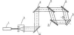
图1、紫外激光干涉灼蚀技术制备金属光栅结构的光路示意图Figure 1. Schematic diagram of the optical path of the metal grating structure fabricated by ultraviolet laser interference ablation technology
其中,1为脉冲紫外激光器;2为介质膜全反镜;3为扩束用透镜组;4为分束镜;5为待加工的样品。Among them, 1 is a pulsed ultraviolet laser; 2 is a dielectric film total reflection mirror; 3 is a lens group for beam expansion; 4 is a beam splitter; 5 is a sample to be processed.
图2、所获得的一维金属光栅结构的光学显微镜照片Figure 2. Optical microscope photo of the obtained one-dimensional metal grating structure
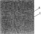
图3、所获得的一维金属光栅结构的扫描电子显微镜(SEM)照片。Fig. 3. A scanning electron microscope (SEM) photo of the obtained one-dimensional metal grating structure.
其中,6标示为金线;7为灼蚀后暴露的基底。Among them, 6 is marked as gold wire; 7 is the substrate exposed after ablation.
具体实施方式Detailed ways
实施例1:一维金纳米线光子晶体结构的制备。Example 1: Preparation of a one-dimensional gold nanowire photonic crystal structure.
1)将化学合成的平均直径为5nm的金纳米颗粒溶解于甲苯或二甲苯等有机溶剂中,制成浓度为100mg/ml的金纳米颗粒胶体溶液;1) dissolving the chemically synthesized gold nanoparticles with an average diameter of 5nm in organic solvents such as toluene or xylene to make a gold nanoparticle colloid solution with a concentration of 100 mg/ml;
2)将金纳米颗粒胶体溶液旋涂在玻璃基底上。旋涂速度为2000rpm,相应的膜厚约为200nm;2) Spin-coat the colloidal solution of gold nanoparticles on the glass substrate. The spin coating speed is 2000rpm, and the corresponding film thickness is about 200nm;
3)将旋涂有金纳米颗粒胶体薄膜的样品放置于加热板上,在250℃下加热25秒,获得厚度均匀、连续的金薄膜结构样品。3) Place the sample spin-coated with the gold nanoparticle colloidal film on a heating plate, and heat it at 250° C. for 25 seconds to obtain a sample with a uniform thickness and continuous gold film structure.
4)将上述制备的金薄膜样品置于干涉光路中,如图1所示,其中两光束的夹角θ=7.8°。利用手动触发使激光器发射一个能量为20mJ,脉冲宽度6ns,波长266nm的激光脉冲,即可在金属薄膜上刻蚀出周期性的一维金属光栅结构。4) Place the above-prepared gold thin film sample in the interference optical path, as shown in Figure 1, where the angle between the two light beams is θ=7.8°. Using manual triggering to make the laser emit a laser pulse with an energy of 20mJ, a pulse width of 6ns, and a wavelength of 266nm, a periodic one-dimensional metal grating structure can be etched on the metal film.
5)所制备的一维金属光栅的结构的光学显微图像如图2所示,在θ=7.8°的情况下,所制备的金属光栅的周期约为1μm。5) The optical microscopic image of the structure of the prepared one-dimensional metal grating is shown in FIG. 2 . In the case of θ=7.8°, the period of the prepared metal grating is about 1 μm.
实施例2:Example 2:
1)将化学合成的平均直径为5nm的金纳米颗粒溶解于甲苯或二甲苯等有机溶剂中,制成浓度为100mg/ml的金纳米颗粒胶体溶液;1) dissolving the chemically synthesized gold nanoparticles with an average diameter of 5nm in organic solvents such as toluene or xylene to make a gold nanoparticle colloid solution with a concentration of 100 mg/ml;
2)将金纳米颗粒胶体溶液旋涂在玻璃基底上。旋涂速度为2000rpm,相应的膜厚约为200nm;2) Spin-coat the colloidal solution of gold nanoparticles on the glass substrate. The spin coating speed is 2000rpm, and the corresponding film thickness is about 200nm;
3)将旋涂有金纳米颗粒胶体薄膜的样品放置于加热板上,在250℃下加热25秒,获得厚度均匀、连续的金薄膜结构样品。3) Place the sample spin-coated with the gold nanoparticle colloidal film on a heating plate, and heat it at 250° C. for 25 seconds to obtain a sample with a uniform thickness and continuous gold film structure.
4)将上述制备的金薄膜样品置于干涉光路中,如图1所示,两束光夹角θ=26.3°。利用手动触发使激光器发射一个能量为20mJ,脉冲宽度6ns,波长266nm的激光脉冲,即可在金属薄膜上刻蚀出周期性的一维金属光栅结构。4) Place the gold thin film sample prepared above in the interference light path, as shown in Figure 1, the angle between the two beams of light is θ=26.3°. Using manual triggering to make the laser emit a laser pulse with an energy of 20mJ, a pulse width of 6ns, and a wavelength of 266nm, a periodic one-dimensional metal grating structure can be etched on the metal film.
5)所制备的一维金属光栅的结构的扫描电子显微镜(SEM)图像如图3所示,金属光栅的周期约为300nm。5) A scanning electron microscope (SEM) image of the structure of the prepared one-dimensional metal grating is shown in FIG. 3 , and the period of the metal grating is about 300 nm.
实施例3:二维金纳米线光子晶体结构的制备Example 3: Preparation of two-dimensional gold nanowire photonic crystal structure
在实施例1已实现的一维金属纳米光栅制备技术的基础上,将样品绕其法线旋转90°,再进行第二次曝光灼蚀,即可实现二维金属纳米光栅结构的制备。On the basis of the one-dimensional metal nano-grating preparation technology realized in Example 1, the sample is rotated 90° around its normal, and then the second exposure and ablation are performed to realize the preparation of a two-dimensional metal nano-grating structure.
Claims (6)
Translated fromChinesePriority Applications (1)
| Application Number | Priority Date | Filing Date | Title |
|---|---|---|---|
| CN 201010265512CN101973512B (en) | 2010-08-30 | 2010-08-30 | Method for directly writing metal micro-nano structure by ultraviolet laser interferometry etching |
Applications Claiming Priority (1)
| Application Number | Priority Date | Filing Date | Title |
|---|---|---|---|
| CN 201010265512CN101973512B (en) | 2010-08-30 | 2010-08-30 | Method for directly writing metal micro-nano structure by ultraviolet laser interferometry etching |
Publications (2)
| Publication Number | Publication Date |
|---|---|
| CN101973512A CN101973512A (en) | 2011-02-16 |
| CN101973512Btrue CN101973512B (en) | 2013-07-10 |
Family
ID=43573428
Family Applications (1)
| Application Number | Title | Priority Date | Filing Date |
|---|---|---|---|
| CN 201010265512Expired - Fee RelatedCN101973512B (en) | 2010-08-30 | 2010-08-30 | Method for directly writing metal micro-nano structure by ultraviolet laser interferometry etching |
Country Status (1)
| Country | Link |
|---|---|
| CN (1) | CN101973512B (en) |
Families Citing this family (10)
| Publication number | Priority date | Publication date | Assignee | Title |
|---|---|---|---|---|
| CN102649196B (en)* | 2011-02-23 | 2015-05-20 | 北京工业大学 | Method for directly writing organic semiconductor laser by ultraviolet laser interferometry etching |
| CN102424356B (en)* | 2011-11-24 | 2014-05-21 | 宁波大学 | Preparation device and method of a metal nanoparticle microarray chip |
| CN103072940B (en)* | 2013-01-15 | 2016-04-27 | 中国计量学院 | A kind of metal micro structure processing method write based on blue laser direct |
| CN103204460B (en)* | 2013-03-21 | 2016-03-02 | 北京工业大学 | Based on the preparation method of the metal micro-nanostructure of laser interference induction cross-linking reaction |
| CN103553364A (en)* | 2013-10-28 | 2014-02-05 | 北京工业大学 | Direct writing method for concentric ring micro-nano structure of metals or/and metallic oxides |
| CN104625420B (en)* | 2014-12-29 | 2016-11-30 | 中自高科(苏州)光电有限公司 | A kind of processing unit (plant) of the antivacuum high conductivity metal nano wire without mask |
| CN105904086A (en)* | 2016-06-20 | 2016-08-31 | 吉林大学 | Laser interference processing device for nano-micro structure on surface of coronary stent through laser guide arms in three-dimensional wave guiding manner |
| CN111185665A (en)* | 2020-01-21 | 2020-05-22 | 武汉铱科赛科技有限公司 | Circuit structure etching method, device, system and equipment |
| CN111880261B (en)* | 2020-08-06 | 2022-05-10 | 温州大学平阳智能制造研究院 | Photonic crystal based on laser etching graphene film stacking and processing method |
| CN111929991A (en)* | 2020-08-10 | 2020-11-13 | 大连理工大学 | Method for rapidly preparing colloidal photonic crystal array chip by utilizing laser direct writing |
Citations (2)
| Publication number | Priority date | Publication date | Assignee | Title |
|---|---|---|---|---|
| CN1821883A (en)* | 2006-01-12 | 2006-08-23 | 苏州大学 | Method and device for microstructure photoetching on smooth surface |
| CN101487976A (en)* | 2009-02-27 | 2009-07-22 | 北京工业大学 | Solution method preparation for metal photon crystal |
- 2010
- 2010-08-30CNCN 201010265512patent/CN101973512B/ennot_activeExpired - Fee Related
Patent Citations (2)
| Publication number | Priority date | Publication date | Assignee | Title |
|---|---|---|---|---|
| CN1821883A (en)* | 2006-01-12 | 2006-08-23 | 苏州大学 | Method and device for microstructure photoetching on smooth surface |
| CN101487976A (en)* | 2009-02-27 | 2009-07-22 | 北京工业大学 | Solution method preparation for metal photon crystal |
Non-Patent Citations (4)
| Title |
|---|
| C. Favazza et al..Self-organized metal nanostructures through laser-interference driven thermocapillary convection.《APPLIED PHYSICS LETTERS》.2007,第91卷第1-3页. |
| Metallic Photonic Crystals Based on Solution-Processible Gold Nanoparticles;Xinping Zhang et al.;《NANO LETTERS》;20060222;第6卷(第4期);第651-655页* |
| Self-organized metal nanostructures through laser-interference driven thermocapillary convection;C. Favazza et al.;《APPLIED PHYSICS LETTERS》;20070725;第91卷;第1-3页* |
| Xinping Zhang et al..Metallic Photonic Crystals Based on Solution-Processible Gold Nanoparticles.《NANO LETTERS》.2006,第6卷(第4期),第651-655页. |
Also Published As
| Publication number | Publication date |
|---|---|
| CN101973512A (en) | 2011-02-16 |
Similar Documents
| Publication | Publication Date | Title |
|---|---|---|
| CN101973512B (en) | Method for directly writing metal micro-nano structure by ultraviolet laser interferometry etching | |
| Wang et al. | Micro‐and nanostructured lead halide perovskites: from materials to integrations and devices | |
| Bushunov et al. | Review of surface modification technologies for mid‐infrared antireflection microstructures fabrication | |
| CN101487976B (en) | Preparation method of metal photonic crystal by solution method | |
| Stelling et al. | Plasmonic nanomeshes: their ambivalent role as transparent electrodes in organic solar cells | |
| CN104656170B (en) | Broadband light full absorber and preparation method thereof | |
| CN103698846B (en) | A kind of preparation method of flexible metal photonic crystal | |
| JP5680552B2 (en) | Method of forming nanowires and related optical component manufacturing method | |
| CN101782666B (en) | Helical metal wire grating circuit polarizer | |
| CN102621128A (en) | Preparation method of large-area sequential controllable surface-enhanced Raman active substrate | |
| CN101551569A (en) | Nonlinear optical material based on metal nanometer cluster array and preparation method thereof | |
| Zhang et al. | Gold nanohole array with sub-1 nm roughness by annealing for sensitivity enhancement of extraordinary optical transmission biosensor | |
| CN101975976B (en) | Photonic crystal micro-nano structure direct-writing method based on metal nanoparticles | |
| CN103344624A (en) | Method for preparing surface-enhanced Raman scattering substrate by solution method and application | |
| CN101856650A (en) | Solution preparation method of localized surface plasmon resonance metal nano-island structure film | |
| KR101175977B1 (en) | Method of fabricating a metal nanopillar array for inducing lspr | |
| Lin et al. | Design and fabrication of photonic crystal structures by single pulse laser interference lithography | |
| Zhang et al. | Solution-processible fabrication of large-area patterned and unpatterned goldnanostructures | |
| KR102272003B1 (en) | A method for forming patterns on a substrate and a substrate prepared by the method | |
| CN103197366B (en) | Polarizing filter based on heterojunction grating and preparation method | |
| CN102651534A (en) | Distributed feedback type organic semiconductor laser preparation method based on laser interferometer lithography | |
| CN102649196B (en) | Method for directly writing organic semiconductor laser by ultraviolet laser interferometry etching | |
| CN114252952B (en) | Double-layer chiral micro-nano structure and preparation method thereof | |
| Qian et al. | Nanosecond Laser Nanopatterning of Highly Ordered Nanodot Arrays on Silicon Surface: Breaking the Monopoly of Femtosecond Lasers | |
| KR20050078017A (en) | Method for forming nanostructure |
Legal Events
| Date | Code | Title | Description |
|---|---|---|---|
| C06 | Publication | ||
| PB01 | Publication | ||
| C10 | Entry into substantive examination | ||
| SE01 | Entry into force of request for substantive examination | ||
| C14 | Grant of patent or utility model | ||
| GR01 | Patent grant | ||
| CF01 | Termination of patent right due to non-payment of annual fee | ||
| CF01 | Termination of patent right due to non-payment of annual fee | Granted publication date:20130710 Termination date:20200830 |