CN101960919A - Hidden organic optoelectronic devices with light-scattering layers - Google Patents
Hidden organic optoelectronic devices with light-scattering layersDownload PDFInfo
- Publication number
- CN101960919A CN101960919ACN2009801066906ACN200980106690ACN101960919ACN 101960919 ACN101960919 ACN 101960919ACN 2009801066906 ACN2009801066906 ACN 2009801066906ACN 200980106690 ACN200980106690 ACN 200980106690ACN 101960919 ACN101960919 ACN 101960919A
- Authority
- CN
- China
- Prior art keywords
- cover layer
- optoelectronic
- light
- particles
- oled
- Prior art date
- Legal status (The legal status is an assumption and is not a legal conclusion. Google has not performed a legal analysis and makes no representation as to the accuracy of the status listed.)
- Pending
Links
Images

Classifications
- B—PERFORMING OPERATIONS; TRANSPORTING
- B82—NANOTECHNOLOGY
- B82Y—SPECIFIC USES OR APPLICATIONS OF NANOSTRUCTURES; MEASUREMENT OR ANALYSIS OF NANOSTRUCTURES; MANUFACTURE OR TREATMENT OF NANOSTRUCTURES
- B82Y20/00—Nanooptics, e.g. quantum optics or photonic crystals
- B—PERFORMING OPERATIONS; TRANSPORTING
- B82—NANOTECHNOLOGY
- B82Y—SPECIFIC USES OR APPLICATIONS OF NANOSTRUCTURES; MEASUREMENT OR ANALYSIS OF NANOSTRUCTURES; MANUFACTURE OR TREATMENT OF NANOSTRUCTURES
- B82Y30/00—Nanotechnology for materials or surface science, e.g. nanocomposites
- H—ELECTRICITY
- H10—SEMICONDUCTOR DEVICES; ELECTRIC SOLID-STATE DEVICES NOT OTHERWISE PROVIDED FOR
- H10K—ORGANIC ELECTRIC SOLID-STATE DEVICES
- H10K10/00—Organic devices specially adapted for rectifying, amplifying, oscillating or switching; Organic capacitors or resistors having potential barriers
- H10K10/80—Constructional details
- H10K10/88—Passivation; Containers; Encapsulations
- H—ELECTRICITY
- H10—SEMICONDUCTOR DEVICES; ELECTRIC SOLID-STATE DEVICES NOT OTHERWISE PROVIDED FOR
- H10K—ORGANIC ELECTRIC SOLID-STATE DEVICES
- H10K30/00—Organic devices sensitive to infrared radiation, light, electromagnetic radiation of shorter wavelength or corpuscular radiation
- H10K30/80—Constructional details
- H10K30/88—Passivation; Containers; Encapsulations
- H—ELECTRICITY
- H10—SEMICONDUCTOR DEVICES; ELECTRIC SOLID-STATE DEVICES NOT OTHERWISE PROVIDED FOR
- H10K—ORGANIC ELECTRIC SOLID-STATE DEVICES
- H10K50/00—Organic light-emitting devices
- H10K50/80—Constructional details
- H10K50/85—Arrangements for extracting light from the devices
- H10K50/854—Arrangements for extracting light from the devices comprising scattering means
- H—ELECTRICITY
- H10—SEMICONDUCTOR DEVICES; ELECTRIC SOLID-STATE DEVICES NOT OTHERWISE PROVIDED FOR
- H10K—ORGANIC ELECTRIC SOLID-STATE DEVICES
- H10K2102/00—Constructional details relating to the organic devices covered by this subclass
- H10K2102/301—Details of OLEDs
- H10K2102/331—Nanoparticles used in non-emissive layers, e.g. in packaging layer
- H—ELECTRICITY
- H10—SEMICONDUCTOR DEVICES; ELECTRIC SOLID-STATE DEVICES NOT OTHERWISE PROVIDED FOR
- H10K—ORGANIC ELECTRIC SOLID-STATE DEVICES
- H10K30/00—Organic devices sensitive to infrared radiation, light, electromagnetic radiation of shorter wavelength or corpuscular radiation
- H10K30/50—Photovoltaic [PV] devices
- H—ELECTRICITY
- H10—SEMICONDUCTOR DEVICES; ELECTRIC SOLID-STATE DEVICES NOT OTHERWISE PROVIDED FOR
- H10K—ORGANIC ELECTRIC SOLID-STATE DEVICES
- H10K30/00—Organic devices sensitive to infrared radiation, light, electromagnetic radiation of shorter wavelength or corpuscular radiation
- H10K30/80—Constructional details
- Y—GENERAL TAGGING OF NEW TECHNOLOGICAL DEVELOPMENTS; GENERAL TAGGING OF CROSS-SECTIONAL TECHNOLOGIES SPANNING OVER SEVERAL SECTIONS OF THE IPC; TECHNICAL SUBJECTS COVERED BY FORMER USPC CROSS-REFERENCE ART COLLECTIONS [XRACs] AND DIGESTS
- Y02—TECHNOLOGIES OR APPLICATIONS FOR MITIGATION OR ADAPTATION AGAINST CLIMATE CHANGE
- Y02E—REDUCTION OF GREENHOUSE GAS [GHG] EMISSIONS, RELATED TO ENERGY GENERATION, TRANSMISSION OR DISTRIBUTION
- Y02E10/00—Energy generation through renewable energy sources
- Y02E10/50—Photovoltaic [PV] energy
- Y02E10/549—Organic PV cells
- Y—GENERAL TAGGING OF NEW TECHNOLOGICAL DEVELOPMENTS; GENERAL TAGGING OF CROSS-SECTIONAL TECHNOLOGIES SPANNING OVER SEVERAL SECTIONS OF THE IPC; TECHNICAL SUBJECTS COVERED BY FORMER USPC CROSS-REFERENCE ART COLLECTIONS [XRACs] AND DIGESTS
- Y02—TECHNOLOGIES OR APPLICATIONS FOR MITIGATION OR ADAPTATION AGAINST CLIMATE CHANGE
- Y02P—CLIMATE CHANGE MITIGATION TECHNOLOGIES IN THE PRODUCTION OR PROCESSING OF GOODS
- Y02P70/00—Climate change mitigation technologies in the production process for final industrial or consumer products
- Y02P70/50—Manufacturing or production processes characterised by the final manufactured product
Landscapes
- Engineering & Computer Science (AREA)
- Chemical & Material Sciences (AREA)
- Nanotechnology (AREA)
- Physics & Mathematics (AREA)
- Crystallography & Structural Chemistry (AREA)
- Optics & Photonics (AREA)
- Biophysics (AREA)
- Life Sciences & Earth Sciences (AREA)
- Composite Materials (AREA)
- Condensed Matter Physics & Semiconductors (AREA)
- General Physics & Mathematics (AREA)
- Materials Engineering (AREA)
- Electromagnetism (AREA)
- Electroluminescent Light Sources (AREA)
- Photovoltaic Devices (AREA)
Abstract
Translated fromChinese
Description
Translated fromChinese技术领域technical field
本发明涉及一种光电器件,该光电器件包括:至少一个光电有源区,所述光电有源区至少包括有机光电材料夹在其间的后电极和前电极,所述后电极是反射的;以及设置在所述前电极之前的覆盖层。The present invention relates to an optoelectronic device comprising: at least one optoelectronic active region comprising at least a rear electrode sandwiched by an organic optoelectronic material and a front electrode, the rear electrode being reflective; and A cover layer is provided in front of the front electrode.
背景技术Background technique
OLED(有机发光二极管)和OPV(有机光生伏打)技术正作为不同类型的照明/再充电用途的替代方案而出现。OLED和OPV统称为有机光电器件。通常,有机光电器件包括有机光电材料夹在其间的两个电极。OLED (Organic Light Emitting Diode) and OPV (Organic Photovoltaic) technologies are emerging as alternatives for different types of lighting/recharging uses. OLEDs and OPVs are collectively referred to as organic optoelectronic devices. Generally, an organic optoelectronic device includes two electrodes with an organic optoelectronic material sandwiched therebetween.
在OLED中,光电材料是电致发光材料。当使电流在这些电极之间流动时,有机电致发光材料发射光。In OLEDs, the optoelectronic material is an electroluminescent material. The organic electroluminescent material emits light when an electric current is caused to flow between these electrodes.
在OPV器件中,光电材料是有机光生伏打材料,其收集光子并且将它们转化成正电荷和负电荷以便在电极之间产生电压。In OPV devices, the optoelectronic material is an organic photovoltaic material that collects photons and converts them into positive and negative charges to generate a voltage between electrodes.
由于有机光电器件的柔性特性,它们可以有利地用于柔性应用,即其中器件在正常操作期间可以弯曲的应用,或者用在弯曲表面上,从而例如在OLED的情况下提供弯曲的显示器件或照明系统。Due to the flexible nature of organic optoelectronic devices, they can be advantageously used in flexible applications, i.e. applications where the device can be bent during normal operation, or on curved surfaces to provide curved display devices or lighting, for example in the case of OLEDs system.
在这个方面,至少当前技术的缺点在于,将光电材料夹在中间的阳极电极和阴极电极之一是高度反射的,以便获得高的光利用。因此,器件具有镜状外观,这在一些应用中是不希望的。例如,OLED在关断状态下的外观是重要的,并且已经提出了不同的解决方案以改善它。In this respect, at least the current technology has the disadvantage that one of the anode and cathode electrodes sandwiching the optoelectronic material is highly reflective in order to obtain high light utilization. Consequently, the device has a mirror-like appearance, which is undesirable in some applications. For example, the appearance of OLEDs in the off state is important and different solutions have been proposed to improve it.
Duggal等人的US 6501218描述了一种利用OLED技术的用于室外标志的器件结构。在这里,被图案化成诸如字符或数字的标志的OLED与光发射OLED区域上的高度散射非吸收涂层以及非发射区域上的高吸收涂层相结合。得益于形成标志(字符、数字)的高度散射材料和形成标志轮廓的高吸收涂层的结合,结果是在低环境光水平条件下可借助于OLED光看到的标志。US 6501218 to Duggal et al. describes a device structure for outdoor signage utilizing OLED technology. Here, OLEDs patterned into signs such as letters or numbers are combined with a highly scattering non-absorbing coating on the light-emitting OLED areas and a highly absorbing coating on the non-emitting areas. Thanks to the combination of the highly scattering material forming the logo (characters, numbers) and the highly absorbing coating forming the logo outline, the result is a logo that is visible by means of OLED light in conditions of low ambient light levels.
US 6501218公开了在OLED顶部上使用散射搪瓷涂层。然而,需要将搪瓷喷涂到塑料膜或载玻片上,然后将其转移到OLED器件。存在对于可以在无需中间涂敷步骤的情况下直接应用到OLED表面的涂层的需要。US 6501218 discloses the use of a scattering enamel coating on top of an OLED. However, the enamel needs to be sprayed onto a plastic film or glass slide, which is then transferred to the OLED device. There is a need for coatings that can be applied directly to the OLED surface without an intermediate coating step.
US 6501218的搪瓷涂层具有以下另外的缺点:当搪瓷涂层已经喷涂于其上的衬底受应力或被弯曲时,该搪瓷涂层将破裂或剥落。The enamel coating of US 6501218 has the further disadvantage that the enamel coating will crack or flake off when the substrate on which the enamel coating has been sprayed is stressed or bent.
此外,在获得包含用于装饰和提供信息的目的的发光图案的大表面方面引起很大关注,并且在许多情况下,如果这些图案仅仅在OLED表面发射光时可见,那么这将是所希望的。Furthermore, there is great interest in obtaining large surfaces containing light-emitting patterns for decorative and informative purposes, and in many cases it would be desirable if these patterns were only visible when the OLED surface emitted light .
此外,引起关注的是提供这样的OPV器件,可以使得该OPV器件对用户不可见,例如以便不干扰被提供有来自OPV的电压的器件的视觉外观。Furthermore, it is of interest to provide such an OPV device which may be rendered invisible to the user, for example so as not to interfere with the visual appearance of the device being supplied with voltage from the OPV.
发明内容Contents of the invention
本发明的目的是至少部分地消除现有技术的至少一些问题,并且提供改进的有机光电器件,该器件基本上对观看者隐蔽,除非它处于其工作状态下。It is an object of the present invention to at least partly obviate at least some of the problems of the prior art and to provide an improved organic optoelectronic device which is substantially hidden from viewers unless it is in its operating state.
因此,在第一方面中,本发明提供了一种光电器件,该光电器件包括:至少一个光电有源区,所述光电有源区至少包括有机光电材料夹在其间的后电极和前电极,所述后电极是反射的;以及设置在所述前电极之前的覆盖层。所述覆盖层包括包含第一材料的光散射颗粒的材料,所述光散射颗粒散布在至少部分地水解的二氧化硅溶胶的透明基质中。Accordingly, in a first aspect, the present invention provides an optoelectronic device comprising: at least one optoelectronic active region comprising at least a rear electrode and a front electrode sandwiched by an organic optoelectronic material, The rear electrode is reflective; and a capping layer disposed in front of the front electrode. The cover layer comprises a material comprising light scattering particles of a first material dispersed in a transparent matrix of at least partially hydrolyzed silica sol.
由于散射颗粒的原因,覆盖层具有高度散射特性。因此,它具有高隐藏能力,使得设置在覆盖层之外的结构不可见。然而,光可以穿过该层。Due to the scattering particles, the cover layer has highly scattering properties. Therefore, it has a high hiding power, making structures arranged outside the covering layer invisible. However, light can pass through this layer.
至少部分地水解的二氧化硅溶胶对于在应力下的破裂具有强的抵抗性,并且因而在所述光电器件很可能经受应力时可以被有利地使用。At least partially hydrolyzed silica sols are highly resistant to cracking under stress and can thus be used advantageously when the optoelectronic device is likely to be subjected to stress.
至少部分地水解的溶胶可以通过使预水解的二氧化硅溶胶干燥来方便地获得,所述干燥可以在室温下进行。该覆盖层材料可以在无需溶剂和/或高温的情况下获得,溶剂和/或高温否则会对OLED功能具有不利的影响。此外,它基本上是非吸收的,并且散射颗粒的包含使得覆盖层高度散射。An at least partially hydrolyzed sol can be conveniently obtained by drying a prehydrolyzed silica sol, which drying can be carried out at room temperature. The cover layer material can be obtained without solvents and/or high temperatures, which would otherwise have a detrimental effect on the function of the OLED. Furthermore, it is essentially non-absorbing, and the inclusion of scattering particles makes the overlay highly scattering.
在本发明的实施例中,光电材料可以是电致发光材料。In an embodiment of the invention, the optoelectronic material may be an electroluminescent material.
如果光电材料是电致发光材料,那么本发明的光电器件是OLED(有机发光二极管)器件。OLED发射光,所述光通过覆盖层进入周围环境中。If the optoelectronic material is an electroluminescent material, the optoelectronic device of the invention is an OLED (Organic Light Emitting Diode) device. The OLED emits light which passes through the cover layer into the surroundings.
OLED发射的光由覆盖层接收,并且该光的一部分(T)透射通过覆盖层。光的另一部分(1-T)往回朝向OLED反射。该光的该部分(R(1-T))在OLED的反射电极中反射之后再次由覆盖层接收,其中R是反射电极的反射率。该二次光的一部分T(1-T)R透射通过覆盖层,而另一部分T(1-T)2R往回朝向OLED反射。这种情况继续下去,直到没有剩余的光透射通过覆盖层。结果,由OLED发射且透射通过覆盖层的光的部分显著高于根据覆盖层的透射率而预期的部分。因此,在工作时,OLED发射的光通过覆盖层是清晰可见的。然而,在非工作状态下,OLED结构通过覆盖层将基本上是不可见的。The light emitted by the OLED is received by the cover layer and a part (T) of this light is transmitted through the cover layer. Another part of the light (1-T) is reflected back towards the OLED. This part of the light (R(1-T)) is received again by the cover layer after being reflected in the reflective electrode of the OLED, where R is the reflectivity of the reflective electrode. A part T(1-T)R of this secondary light is transmitted through the cover layer, while another part T(1-T)2 R is reflected back towards the OLED. This continues until no remaining light is transmitted through the cover layer. As a result, the fraction of light emitted by the OLED and transmitted through the cover layer is significantly higher than would be expected from the transmittance of the cover layer. Thus, during operation, the light emitted by the OLED is clearly visible through the cover layer. However, in the non-operating state, the OLED structure will be substantially invisible through the cover layer.
在本发明的其它实施例中,有机光电材料可以是有机光生伏打材料。In other embodiments of the present invention, the organic optoelectronic material may be an organic photovoltaic material.
如果光电材料是有机光生伏打材料,则本发明的器件是能够将光转化成电压的OPV(有机光生伏打器件)。If the optoelectronic material is an organic photovoltaic material, the device of the invention is an OPV (Organic Photovoltaic Device) capable of converting light into electrical voltage.
依照本发明将OPV设置在覆盖层之后使得OPV的结构对观看者不可见,以便它们可以隐藏在其中需要这种OPV的不同器件中。OPV对于漫射光工作良好,因而覆盖层的散射特性不妨碍OPV的功能。Placing the OPVs behind the cover layer according to the present invention makes the structures of the OPVs invisible to the viewer so that they can be hidden in different devices where such OPVs are needed. OPVs work well for diffuse light, so the scattering properties of the cover layer do not interfere with the function of the OPV.
应当指出的是,依照本发明的器件可以包括有机电致发光材料和有机光生伏打材料这两者,例如该器件的一个区域充当基于有机的发光器件,该器件的另一区域充当基于有机的太阳能电池。It should be noted that a device according to the invention may comprise both organic electroluminescent material and organic photovoltaic material, e.g. one region of the device acts as an organic-based light-emitting device and another region of the device acts as an organic-based light-emitting device. Solar battery.
在本发明的实施例中,所述覆盖层叠加在所述至少一个光电有源区上并且至少覆盖所述至少一个光电有源区的整个表面。In an embodiment of the present invention, the covering layer is superimposed on the at least one optoelectronic active region and at least covers the entire surface of the at least one optoelectronic active region.
利用覆盖层覆盖整个光电表面隐藏了所述光电器件,即使得它对于观看者基本上不可见。在OLED器件中,它可以保持隐蔽,直到器件处于其工作状态。Covering the entire optoelectronic surface with a cover layer hides the optoelectronic device, ie makes it substantially invisible to the viewer. In OLED devices, it can remain hidden until the device is in its operational state.
在本发明的实施例中,所述器件可以包括至少第一和第二光电有源区,所述光电有源区并排设置并且相互分隔开以便在其间形成间隙区,其中所述覆盖层叠加在所述第一和第二光电有源区上并且至少覆盖所述第一和第二光电有源区和所述间隙区的组合表面。In an embodiment of the present invention, the device may comprise at least first and second optoelectronic active regions arranged side by side and spaced apart from each other to form a gap region therebetween, wherein the cover layer overlaps On the first and second optoelectronic active regions and covering at least the combined surface of the first and second optoelectronic active regions and the gap region.
利用同一个覆盖层覆盖两个或更多OLED以及这些OLED之间的间隙提供了一种光模式,其可以在覆盖层表面上显示,即使发光器件如上面所讨论的被隐蔽,直到处于其工作状态。在光生伏打器件的情况下,覆盖层的表面将不显露设置在其后的多个器件的存在。Covering two or more OLEDs with the same cover layer and the gaps between these OLEDs provides a light pattern that can be displayed on the cover layer surface even if the light emitting device is concealed as discussed above until in its operating state. state. In the case of photovoltaic devices, the surface of the cover layer will not reveal the presence of devices disposed therebehind.
在本发明的实施例中,所述透明基质是二氧化硅溶胶凝胶。In an embodiment of the present invention, the transparent matrix is silica sol-gel.
溶胶凝胶可以通过进一步使部分地水解的二氧化硅溶胶干燥来获得。这可以在室温下或者至少在不损坏光电部件的温度下并且也在不使用诸如溶剂之类的对光电部件有害的化合物的情况下进行。二氧化硅溶胶凝胶还是玻璃状材料,其对于例如刮擦的机械影响具有良好的抵抗性。Sol-gel can be obtained by further drying the partially hydrolyzed silica sol. This can be done at room temperature or at least at a temperature which does not damage the optoelectronic component and also without using compounds which are harmful to the optoelectronic component, such as solvents. Silica sol-gels are also glass-like materials which have good resistance to mechanical influences such as scratching.
在本发明的实施例中,所述覆盖层可以具有从50%到95%的范围内的反射率。In an embodiment of the invention, the cover layer may have a reflectivity ranging from 50% to 95%.
优选地,覆盖层的反射率处于所述范围内以便维持隐藏(一个或多个)光电器件的结构的能力与发射足够的光的能力之间的折衷。在OLED器件的情况下,OLED在非工作状态下隐藏,而覆盖层允许(一个或多个)OLED发射的光穿过。Preferably, the reflectivity of the cover layer is within said range so as to maintain a compromise between the ability to hide the structure of the optoelectronic device(s) and the ability to emit sufficient light. In the case of OLED devices, the OLEDs are hidden in the non-operating state, while the cover layer allows the light emitted by the OLED(s) to pass through.
在本发明的实施例中,所述第一材料的所述颗粒的折射率高于透明基质的折射率。In an embodiment of the invention, said particles of said first material have a higher refractive index than the transparent matrix.
通过将高折射率颗粒散布在低折射率材料中,获得良好的散射效应。A good scattering effect is obtained by dispersing high refractive index particles in a low refractive index material.
在本发明的实施例中,所述第一材料的所述颗粒按重量计算占所述覆盖层材料的大约10%到大约80%,优选地按重量计算占15%到70%。In an embodiment of the invention, said particles of said first material comprise from about 10% to about 80% by weight of said cover layer material, preferably from 15% to 70% by weight.
光散射颗粒以上面的浓度包含在覆盖层中以便赋予覆盖层良好的散射效应。The light-scattering particles are contained in the cover layer in the above concentration in order to impart a good scattering effect to the cover layer.
在第二方面中,本发明涉及包括本发明第一方面的器件的装置,该器件设置在至少部分地包围所述器件的侧向边缘的框架中,其中所述覆盖层覆盖所述至少一个器件以及所述框架的至少一部分。In a second aspect, the present invention relates to a device comprising a device according to the first aspect of the invention, the device being arranged in a frame at least partially surrounding the lateral edges of said device, wherein said cover layer covers said at least one device and at least a portion of the frame.
利用相同的覆盖材料覆盖所述(一个或多个)光电器件及其周围的框架这两者使得有效地隐藏光电器件成为可能,因为从框架到OLED的转变在(OLED的)非工作状态下将不容易通过仅仅视觉检查而从外部检测到。Covering both the optoelectronic device(s) and the surrounding frame with the same cover material makes it possible to effectively hide the optoelectronic device, since the transition from the frame to the OLED will in the non-operating state (of the OLED) Not easily detectable from the outside by mere visual inspection.
在第三方面中。本发明涉及一种用于制造依照本发明的光电器件的方法,该方法包括步骤:提供光电器件;向可选地预水解的二氧化硅溶胶提供散布于其中的所述第一材料的颗粒;将所述二氧化硅溶胶层设置在所述光电器件的所述前电极之前;以及使所述层干燥。In the third aspect. The invention relates to a method for manufacturing an optoelectronic device according to the invention, the method comprising the steps of: providing an optoelectronic device; providing an optionally prehydrolyzed silica sol with particles of said first material dispersed therein; disposing the silica sol layer in front of the front electrode of the photovoltaic device; and drying the layer.
应当进一步指出的是,本发明涉及所附权利要求的所有可能的组合。It should be further noted that the invention relates to all possible combinations of the appended claims.
附图说明Description of drawings
现在,将参照示出本发明当前优选实施例的附图更详细地描述本发明的这些和其它方面。These and other aspects of the invention will now be described in more detail with reference to the accompanying drawings showing presently preferred embodiments of the invention.
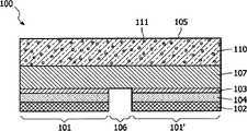
图1以截面图示意性地示出了本发明的发光器件。Fig. 1 schematically shows a light emitting device of the present invention in a cross-sectional view.
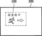
图2a以平面视图示意性地示出了关断状态下本发明的基于OLED的装置。Figure 2a schematically shows the OLED-based device of the invention in the off state in plan view.
图2b以平面视图示意性地示出了接通状态下图2a的装置。FIG. 2b schematically shows the device of FIG. 2a in the switched-on state in plan view.
具体实施方式Detailed ways
本发明涉及包括电极对的有机光电器件,所述电极对即有机光电材料夹在其间的后电极和前电极,后电极是反射的,而覆盖层设置在前电极之前。The invention relates to an organic optoelectronic device comprising a pair of electrodes, namely a back electrode and a front electrode sandwiched between an organic optoelectronic material, the back electrode being reflective and a cover layer placed in front of the front electrode.
图1中示意性地示出了依照本发明的发光器件100,即其中有机光电材料是电致发光材料的有机光电器件,并且该发光器件包括两个OLED有源区101和101’。每个OLED有源区101、101’包括有机电致发光材料104,该材料设置在(即,夹在)后电极102与前电极103之间。OLED有源区101被定义为其中电致发光材料104夹在两个电极102、103之间的区域。相邻OLED有源区101、101’之间的区域在下文中表示为间隙区106。A
当在本文中使用时,就覆盖层设置在前电极之前的语境而言,措辞“设置在……之前”表示覆盖层设置在器件的前电极与器件的外部环境之间。对于OLED器件而言,这意味着覆盖层接收OLED发射的光并且将其传递到环境中。对于OPV器件而言,这意味着环境光在其穿过前电极并且到达光生伏打层之前穿过覆盖层。As used herein, in the context of a covering layer being disposed in front of the front electrode, the expression "disposed in front of" means that the covering layer is disposed between the front electrode of the device and the external environment of the device. For OLED devices, this means that the cover layer receives the light emitted by the OLED and transmits it to the environment. For an OPV device, this means that ambient light passes through the cover layer before it passes through the front electrode and reaches the photovoltaic layer.
在图1的实施例中,前电极103是透明的,从而它代表OLED器件的发光(前)侧,而后电极102是反射的。In the embodiment of Fig. 1, the
适合于电极的材料以及有机电致发光或有机光生伏打材料对于本领域技术人员应当是已知的,并且在此将不详细讨论。但是,典型地,透射前电极可以由诸如ITO(氧化铟锡)之类的透明导电材料制成,并且反射后电极可以由诸如金属或涂敷了金属的材料之类的反射导电材料制成。Materials suitable for electrodes as well as organic electroluminescent or organic photovoltaic materials should be known to those skilled in the art and will not be discussed in detail here. Typically, however, the transmissive front electrode may be made of a transparent conductive material such as ITO (Indium Tin Oxide), and the reflective rear electrode may be made of a reflective conductive material such as metal or metallized material.
有机光电材料可以是聚合物材料或者具有小的有机分子的材料,如本领域中所公知的。Organic optoelectronic materials can be polymeric materials or materials with small organic molecules, as known in the art.
如本领域中所已知的,光电器件常规上还可以包括附加层,例如阻挡层、用于均匀电流分布的金属分流器、缓冲层和衬底。然而,为了简单起见,省略了对这样的层的描述,因为它们的位置和用途对于本领域技术人员而言是熟知的。诸如发光器件100之类的光电器件典型地还包括本领域中常规的驱动电子部件(未示出)。As is known in the art, optoelectronic devices may also conventionally include additional layers, such as barrier layers, metal shunts for uniform current distribution, buffer layers, and substrates. However, descriptions of such layers are omitted for simplicity since their positions and uses are well known to those skilled in the art. An optoelectronic device such as light emitting
覆盖层105设置在OLED有源区101、101’之上、前电极103之前,并且也覆盖位于这些有源区之间的间隙区106。A
覆盖层105设置在衬底107上,该衬底位于前电极与覆盖层105之间。该衬底可以例如由玻璃或塑料形成,并且可以例如包括保护有源层不受水和/或氧气影响的缓冲层。The
覆盖层包括其中散布散射颗粒110的至少部分地水解的二氧化硅(silica)溶胶凝胶的基本上非吸收基质111。The cover layer comprises an essentially
典型地,基质111是二氧化硅溶胶凝胶,其具有是透明、坚硬、防刮和玻璃状的材料的优点。Typically, the
散射颗粒110典型地由具有比周围基质111的折射率更高的折射率的材料形成。例如,散射颗粒的折射率优选地为至少2.0。周围基质典型地具有大约1.3至1.6的折射率。The scattering
散射颗粒110典型地由选自包括TiO2锐钛矿、TiO2金红石、ZrO2、Ta2O5、ZnS、ZnSe或者其中两种或更多种的混合物的组的材料制成。The scattering
这些材料是适合于要散布在所述基质中的基本上非吸收的散射颗粒的材料的良好实例。These materials are good examples of materials suitable for the substantially non-absorbing scattering particles to be dispersed in the matrix.
散射颗粒典型地按重量计算占所述覆盖层材料的大约10%到大约80%,优选地按重量计算占15%到70%。Scattering particles typically comprise from about 10% to about 80% by weight of the cover layer material, preferably from 15% to 70% by weight.
光散射颗粒以上面给定范围内的浓度包含在覆盖层中以便在覆盖层中提供良好的散射效应。The light-scattering particles are contained in the cover layer in a concentration within the range given above in order to provide a good scattering effect in the cover layer.
散射颗粒110的颗粒尺寸可以被选择成匹配OLED发射的光的颜色以便获得最大的散射效应。平均颗粒尺寸应当接近用于此的发射的光的波长。因此,散射颗粒的平均颗粒尺寸范围为从100nm到1000nm,优选地从200nm到800nm(即从UV到可见光的波长范围)。The particle size of the scattering
典型地选择基质中散射颗粒110的浓度以及覆盖层105的厚度以便获得这样的涂层,该涂层当OLED有源区处于非工作(关断)状态时隐蔽OLED结构,但是允许OLED有源区发射的光通过覆盖层105发出。The concentration of scattering
典型地,具有大于每次通过50%的反射率的涂层是所希望的,该反射率优选地大于75%,例如大于85%,由此获得良好的隐藏能力。Typically, a coating having a reflectivity of greater than 50% per pass is desired, preferably greater than 75%, such as greater than 85%, whereby good hiding power is obtained.
覆盖层的厚度典型地从1μm到50μm以便提供良好的隐藏特性和希望的透射率。The thickness of the cover layer is typically from 1 μm to 50 μm in order to provide good hiding properties and desired transmittance.
在理想的情况下,采用非吸收覆盖层,OLED发射的光通过覆盖层的总透射可以计算为In the ideal case, with a non-absorbing cover layer, the total transmission of light emitted by the OLED through the cover layer can be calculated as
其中T为每次通过覆盖层的透射(1-反射率)并且R为OLED有源区的反射电极的反射率。where T is the transmission (1-reflectivity) per pass through the cover layer and R is the reflectivity of the reflective electrode of the active region of the OLED.
对于作为本发明器件的代表值的20%的T值(80%的反射)和80%的R值,Ttot等于0.6。For a T value of 20% (reflection of 80%) and an R value of 80%, which are representative values of the device of the present invention, Ttot is equal to 0.6.
因此,OLED有源区发射的光将通过覆盖层而清晰可见,而OLED结构在关断状态下通过覆盖层将基本上不可见。覆盖层105可以例如通过如下方式获得。Thus, the light emitted by the active region of the OLED will be clearly visible through the cover layer, while the OLED structure will be substantially invisible through the cover layer in the off state. The
二氧化硅前体溶胶凝胶通过例如利用充当催化剂的酸在水中预水解烷氧基硅烷(alkoxysilane)溶液而获得。Silica precursor sol-gels are obtained, for example, by prehydrolysis of alkoxysilane solutions in water with acids acting as catalysts.
将二氧化硅颗粒的悬浮液添加到预水解溶胶。然后,将散射颗粒110添加到该混合物。A suspension of silica particles was added to the prehydrolyzed sol. Then, scattering
得到的混合物于是可以通过本领域技术人员已知的方式(例如滚轧工作台)来均质化。结果是稳定的悬浮液。如果保持在冷冻装置中,那么该悬浮液具有至少两个月的保存期。The resulting mixture can then be homogenized by means known to the person skilled in the art, for example a rolling bench. The result is a stable suspension. If kept in a freezer, the suspension has a shelf life of at least two months.
然后,可以借助于诸如旋涂、喷涂或者刮涂之类的任何常规使用的涂敷方法将悬浮液涂敷到OLED表面上。The suspension can then be applied to the OLED surface by means of any conventionally used coating method such as spin coating, spray coating or blade coating.
涂敷层允许在室温下干燥,无需进一步的热处理就获得具有透射与隐藏特性之间的希望的折衷的硬保护覆盖层。The coating layer is allowed to dry at room temperature, obtaining a hard protective cover layer with the desired compromise between transmission and hiding properties without further heat treatment.
使用的OLED可以是均匀的瓦状物,或者可以具有图案化的图画或者其它在涂敷之前可见的创造气氛的设计。The OLEDs used may be uniform tiles, or may have patterned drawings or other ambience-creating designs visible prior to coating.
本领域技术人员容易理解的是,如果有机电致发光材料被有机光生伏打材料代替,那么上面描述的实施例也可以应用于有机光生伏打器件(OPV)中。Those skilled in the art can easily understand that if the organic electroluminescent material is replaced by an organic photovoltaic material, the above-described embodiments can also be applied in an organic photovoltaic device (OPV).
典型地,OPV(也称为有机太阳能电池)用于通过将诸如阳光或室内光之类的光转换成电能而驱动某些种类的电子器件(例如OLED)。对于观看者隐蔽的本发明的OPV在许多应用中是有利的,例如希望OPV应当不干扰OPV向其提供电压的器件的视觉外观的情况。由于OPV不再可见,因而从设计的观点来看增强了该方法的可应用性。这样的应用的实例包括但不限于太阳能电池驱动的手表、PDA、移动电话等等,其中OPV充当所述太阳能电池。Typically, OPVs (also known as organic solar cells) are used to drive certain kinds of electronic devices (such as OLEDs) by converting light, such as sunlight or indoor light, into electrical energy. The OPV of the present invention which is concealed from a viewer is advantageous in many applications, for example where it is desired that the OPV should not interfere with the visual appearance of the device to which the OPV supplies voltage. Since the OPV is no longer visible, the applicability of the method is enhanced from a design point of view. Examples of such applications include, but are not limited to, solar cell powered watches, PDAs, mobile phones, etc. where the OPV acts as the solar cell.
对于OPV的功能,可以非常充分地散射所利用的光,因为这不大影响器件的光转换效率。因此,OPV可以像在本发明中那样有利地位于覆盖层之后。For the function of the OPV, the light used can be scattered very well, since this does not affect the light conversion efficiency of the device much. Thus, the OPV can advantageously be located behind the covering layer as in the present invention.
然而,如果本发明的光电器件是OPV,那么覆盖层的透射率优选地不像上面在OLED实施例中描述的那样受限。取而代之,覆盖层典型地被选择成具有每次通过至少20%的透射率(每次通过低于80%的反射),例如每次通过至少50%的透射率。然而,覆盖层典型地被选择成具有良好的隐藏特性,即高度散射的。However, if the optoelectronic device of the present invention is an OPV, the transmissivity of the cover layer is preferably not as limited as described above in the OLED embodiment. Instead, the cover layer is typically selected to have a transmission of at least 20% per pass (less than 80% reflection per pass), such as at least 50% transmission per pass. However, the cover layer is typically chosen to have good hiding properties, ie to be highly scattering.
本发明的器件可以嵌入在至少部分地被表面材料框架包围的表面中,其中器件和框架材料均由相同的覆盖层材料涂敷。因此,器件的位置将对观看者隐蔽(在OLED器件的情况下,至少直到器件处于其接通状态并且发射光)。这可以根据需要用在大量的应用中,以便快速地在墙壁上呈现信息、警告标志或艺术图案。The device of the invention may be embedded in a surface at least partially surrounded by a frame of surface material, wherein both the device and the frame material are coated with the same cover material. Thus, the position of the device will be hidden from the viewer (in the case of an OLED device, at least until the device is in its on state and emitting light). This can be used in a multitude of applications as needed to quickly present information, warning signs or artwork on walls.
图2a和图2b中示出了包括嵌入到普通墙壁200中的本发明的发光器件100的这种装置。在图2a中,发光器件处于关断状态,并且虚线仅仅表示发光器件100的位置。在墙壁200中切出开口以形成发光器件100设置于其中的框架。覆盖层105不仅用来涂敷发光器件100,而且用来涂敷墙壁200。Such an arrangement comprising a
在图2b中,当发光器件100接通时,在墙壁上点亮了文本“安全出口”和指向希望的方向的箭头。这显然仅仅代表设置在周围材料的框架中的发光器件的装置的一种可能用途。In Fig. 2b, when the
本发明中使用的基于二氧化硅溶胶凝胶的覆盖层材料不仅粘附到OLED表面,而且粘附到其它表面,这些其它表面例如但不限于玻璃、金属、陶瓷、塑料或木制表面。因此,本发明的发光器件可以设置在几乎任何材料的框架中。由于可以在柔性/可弯曲实施例中制造OLED发光器件,因而本发明的发光器件可以设置在例如柱形物等的弯曲表面中。The silica sol-gel based overlay material used in the present invention adheres not only to the OLED surface but also to other surfaces such as but not limited to glass, metal, ceramic, plastic or wooden surfaces. Thus, the light-emitting device of the invention can be arranged in a frame of almost any material. Since the OLED light emitting device can be fabricated in a flexible/bendable embodiment, the light emitting device of the present invention can be placed in a curved surface such as a pillar or the like.
本领域技术人员应当认识到,其中光电器件和框架材料均由相同覆盖层材料涂敷的光电器件部分地被框架包围的这种装置也可以应用到OPV器件。Those skilled in the art will realize that such an arrangement in which the optoelectronic device and the frame material are both coated with the same cover layer material and the optoelectronic device is partially surrounded by the frame can also be applied to OPV devices.
在上面描述的实施例中,覆盖层覆盖不止光电器件的有源区。然而,在本发明的其它实施例(未示出)中,覆盖层仅仅或者基本上仅仅覆盖(一个或多个)有源区,使得即使光电器件的实际层结构被覆盖层隐蔽,(一个或多个)有源区的形状或图案也清晰可见。例如,可以通过引入染料或色素使得覆盖层清晰可见。In the embodiments described above, the cover layer covers more than the active area of the optoelectronic device. However, in other embodiments of the invention (not shown), the cover layer only or substantially only covers the active region(s), so that even if the actual layer structure of the optoelectronic device is concealed by the cover layer, (one or The shapes or patterns of the active regions are also clearly visible. For example, the cover layer can be made visible by introducing dyes or pigments.
本领域技术人员应当认识到,本发明绝不限于上面描述的优选实施例。相反地,许多修改和变型都可能处于所附权利要求的范围内。Those skilled in the art will realize that the present invention is by no means limited to the preferred embodiments described above. On the contrary, many modifications and variations are possible within the scope of the appended claims.
例如,覆盖层材料可以包含色素或染料以便赋予覆盖层希望的颜色。For example, the cover material may contain pigments or dyes to impart a desired color to the cover.
Claims (15)
Translated fromChineseApplications Claiming Priority (3)
| Application Number | Priority Date | Filing Date | Title |
|---|---|---|---|
| EP08152016.5 | 2008-02-27 | ||
| EP08152016 | 2008-02-27 | ||
| PCT/IB2009/050686WO2009107043A1 (en) | 2008-02-27 | 2009-02-19 | Hidden organic optoelectronic devices with a light scattering layer |
Related Child Applications (1)
| Application Number | Title | Priority Date | Filing Date |
|---|---|---|---|
| CN201410096688.8ADivisionCN103824960A (en) | 2008-02-27 | 2009-02-19 | Hidden organic optoelectronic devices with a light scattering layer |
Publications (1)
| Publication Number | Publication Date |
|---|---|
| CN101960919Atrue CN101960919A (en) | 2011-01-26 |
Family
ID=40718804
Family Applications (2)
| Application Number | Title | Priority Date | Filing Date |
|---|---|---|---|
| CN201410096688.8APendingCN103824960A (en) | 2008-02-27 | 2009-02-19 | Hidden organic optoelectronic devices with a light scattering layer |
| CN2009801066906APendingCN101960919A (en) | 2008-02-27 | 2009-02-19 | Hidden organic optoelectronic devices with light-scattering layers |
Family Applications Before (1)
| Application Number | Title | Priority Date | Filing Date |
|---|---|---|---|
| CN201410096688.8APendingCN103824960A (en) | 2008-02-27 | 2009-02-19 | Hidden organic optoelectronic devices with a light scattering layer |
Country Status (9)
| Country | Link |
|---|---|
| US (2) | US8552446B2 (en) |
| EP (1) | EP2248391B1 (en) |
| JP (1) | JP5791904B2 (en) |
| CN (2) | CN103824960A (en) |
| AT (1) | ATE535028T1 (en) |
| ES (1) | ES2377598T3 (en) |
| RU (1) | RU2480967C2 (en) |
| TW (1) | TW200945645A (en) |
| WO (1) | WO2009107043A1 (en) |
Cited By (4)
| Publication number | Priority date | Publication date | Assignee | Title |
|---|---|---|---|---|
| CN102299266A (en)* | 2011-09-15 | 2011-12-28 | 四川虹视显示技术有限公司 | Substrate of organic light-emitting diode (OLED) and manufacturing method for substrate |
| CN103311332A (en)* | 2012-03-12 | 2013-09-18 | 杜邦太阳能有限公司 | Solar module and manufacturing method thereof |
| CN105247702A (en)* | 2013-09-30 | 2016-01-13 | 株式会社Lg化学 | Organic Electronic Devices |
| CN105684173A (en)* | 2013-11-08 | 2016-06-15 | 奥斯兰姆奥普托半导体有限责任公司 | Optoelectronic component, optoelectronic arrangement, method for producing an optical element, and method for producing an optoelectronic component |
Families Citing this family (15)
| Publication number | Priority date | Publication date | Assignee | Title |
|---|---|---|---|---|
| CN103329284B (en)* | 2011-01-24 | 2016-08-03 | Lg化学株式会社 | Photovoltaic battery module |
| TWI463717B (en)* | 2011-07-29 | 2014-12-01 | Au Optronics Corp | Organic light-emitting element, manufacturing method thereof and lighting device using same |
| KR101353434B1 (en)* | 2011-10-17 | 2014-01-21 | 주식회사 엘지화학 | Substrate for organic electronic device |
| KR20130111155A (en)* | 2012-03-30 | 2013-10-10 | 주식회사 엘지화학 | Substrate for organic electronic devices |
| US20150122324A1 (en)* | 2012-05-18 | 2015-05-07 | Brookhaven Science Associates, Llc | Thin-film photovoltaic device with optical field confinement and method for making same |
| KR101475331B1 (en)* | 2013-02-22 | 2014-12-22 | 주식회사 창강화학 | Scattering member and organic Lighting Emitting display apparatus having the same |
| EP3034548A1 (en)* | 2014-12-18 | 2016-06-22 | Nederlandse Organisatie voor toegepast- natuurwetenschappelijk onderzoek TNO | Barrier film laminate comprising submicron getter particles and electronic device comprising such a laminate |
| DE102015101683A1 (en)* | 2015-02-05 | 2016-08-11 | Osram Oled Gmbh | Light-emitting device and method for producing a light-emitting device |
| US10340844B2 (en)* | 2016-05-05 | 2019-07-02 | Washington State University | High-performance planar solar concentrators based on nanoparticle doping |
| CN109844975A (en)* | 2016-07-20 | 2019-06-04 | 华为技术有限公司 | Organic light emitting display and method for manufacturing organic light emitting display |
| CN106292074B (en)* | 2016-10-17 | 2020-03-31 | 纳晶科技股份有限公司 | Photoluminescent device and luminescent device with same |
| EP3421278B1 (en)* | 2017-06-29 | 2022-10-19 | PLASMAN Europe AB | Illuminated decorative strip |
| CN110277503A (en)* | 2018-03-14 | 2019-09-24 | 江苏三月光电科技有限公司 | Organic light-emitting device and its preparation method |
| CN108987382A (en)* | 2018-07-27 | 2018-12-11 | 京东方科技集团股份有限公司 | A kind of electroluminescent device and preparation method thereof |
| KR102137258B1 (en)* | 2020-01-13 | 2020-07-22 | 부경대학교 산학협력단 | Variable color photovoltaic module using double sided dot printing and manufacturing method of the same |
Family Cites Families (31)
| Publication number | Priority date | Publication date | Assignee | Title |
|---|---|---|---|---|
| DE3151350A1 (en)* | 1981-12-24 | 1983-07-07 | Bayer Ag, 5090 Leverkusen | PLASTIC MOLDED BODIES EQUIPPED WITH A 3-LAYER COVER AND A METHOD FOR PRODUCING THE EQUIPMENT |
| JPH0529641A (en)* | 1991-10-04 | 1993-02-05 | Seikosha Co Ltd | Solar battery device |
| BE1007282A3 (en)* | 1993-07-12 | 1995-05-09 | Philips Electronics Nv | An opto-electronic semiconductor device with an array of semiconductor diode lasers and a method for the production thereof. |
| WO1996034514A1 (en)* | 1995-04-25 | 1996-10-31 | Citizen Watch Co., Ltd. | Organic electroluminescence apparatus |
| JP3394718B2 (en)* | 1995-04-25 | 2003-04-07 | シチズン時計株式会社 | Organic electroluminescence device |
| GB9522135D0 (en) | 1995-10-30 | 1996-01-03 | John Mcgavigan Holdings Limite | Display panels |
| CN1263354A (en)* | 1999-02-12 | 2000-08-16 | 同济大学 | Wide band antireflective nano-coating layer for glass display screen and its production method |
| US20020003403A1 (en)* | 2000-04-25 | 2002-01-10 | Ghosh Amalkumar P. | Thin film encapsulation of organic light emitting diode devices |
| US6501218B1 (en)* | 2000-06-12 | 2002-12-31 | General Electric Company | Outdoor electroluminescent display devices |
| JP4230170B2 (en)* | 2001-06-08 | 2009-02-25 | 株式会社半導体エネルギー研究所 | Method for manufacturing light emitting device |
| JP2003004916A (en)* | 2001-06-20 | 2003-01-08 | Dainippon Printing Co Ltd | Window material for display device, method for manufacturing the same, and display device |
| WO2003026357A1 (en)* | 2001-09-13 | 2003-03-27 | Nissan Chemical Industries, Ltd. | Organic electroluminescence element-use transparent substrate and organic electroluminescence element |
| ITTO20020033A1 (en)* | 2002-01-11 | 2003-07-11 | Fiat Ricerche | ELECTRO-LUMINESCENT DEVICE. |
| CN1503009A (en)* | 2002-11-20 | 2004-06-09 | 力特光电科技股份有限公司 | anti-glare film |
| GB0302550D0 (en)* | 2003-02-05 | 2003-03-12 | Cambridge Display Tech Ltd | Organic optoelectronic device |
| WO2004089042A1 (en)* | 2003-03-12 | 2004-10-14 | Mitsubishi Chemical Corporation | Electroluminescence device |
| CN100463578C (en)* | 2003-03-12 | 2009-02-18 | 三菱化学株式会社 | Electroluminescent element |
| DE102004026730A1 (en) | 2004-05-28 | 2005-12-15 | Manfred Kluth | Surface with electrical consumers, in particular bulbs |
| US20060066586A1 (en)* | 2004-09-27 | 2006-03-30 | Gally Brian J | Touchscreens for displays |
| EP1860919B1 (en) | 2005-03-11 | 2012-02-15 | Mitsubishi Chemical Corporation | Electroluminescence element and lighting apparatus |
| US20060290276A1 (en)* | 2005-06-22 | 2006-12-28 | Eastman Kodak Company | OLED device having spacers |
| WO2007035529A2 (en) | 2005-09-16 | 2007-03-29 | University Of Washington | Thin-profile therapeutic ultrasound applicators |
| JP2007180014A (en)* | 2005-11-30 | 2007-07-12 | Alps Electric Co Ltd | Light emitting device and method of manufacturing same |
| GB0602678D0 (en)* | 2006-02-09 | 2006-03-22 | Dupont Teijin Films Us Ltd | Polyester film and manufacturing process |
| US7791271B2 (en)* | 2006-02-24 | 2010-09-07 | Global Oled Technology Llc | Top-emitting OLED device with light-scattering layer and color-conversion |
| WO2007107903A1 (en) | 2006-03-23 | 2007-09-27 | Koninklijke Philips Electronics N.V. | Led-based lighting device with colour control |
| KR101460813B1 (en)* | 2006-09-29 | 2014-11-11 | 오스람 옵토 세미컨덕터스 게엠베하 | Organic light emitting devices and lighting devices |
| TWI326923B (en)* | 2007-03-07 | 2010-07-01 | Lite On Technology Corp | White light emitting diode |
| TW200926454A (en)* | 2007-08-03 | 2009-06-16 | Panasonic Corp | Light-emitting device |
| JP2009070515A (en)* | 2007-09-14 | 2009-04-02 | Mitsubishi Chemicals Corp | Optical recording medium |
| KR101318072B1 (en)* | 2008-06-04 | 2013-10-15 | 엘지디스플레이 주식회사 | Organic light emitting diode display device and method fabricating the same |
- 2009
- 2009-02-19USUS12/918,563patent/US8552446B2/enactiveActive
- 2009-02-19WOPCT/IB2009/050686patent/WO2009107043A1/enactiveApplication Filing
- 2009-02-19CNCN201410096688.8Apatent/CN103824960A/enactivePending
- 2009-02-19CNCN2009801066906Apatent/CN101960919A/enactivePending
- 2009-02-19JPJP2010548223Apatent/JP5791904B2/enactiveActive
- 2009-02-19RURU2010139474/07Apatent/RU2480967C2/enactive
- 2009-02-19ATAT09713749Tpatent/ATE535028T1/enactive
- 2009-02-19ESES09713749Tpatent/ES2377598T3/enactiveActive
- 2009-02-19EPEP09713749Apatent/EP2248391B1/enactiveActive
- 2009-02-24TWTW098105830Apatent/TW200945645A/enunknown
- 2013
- 2013-09-20USUS14/032,245patent/US9040970B2/enactiveActive
Cited By (6)
| Publication number | Priority date | Publication date | Assignee | Title |
|---|---|---|---|---|
| CN102299266A (en)* | 2011-09-15 | 2011-12-28 | 四川虹视显示技术有限公司 | Substrate of organic light-emitting diode (OLED) and manufacturing method for substrate |
| CN103311332A (en)* | 2012-03-12 | 2013-09-18 | 杜邦太阳能有限公司 | Solar module and manufacturing method thereof |
| CN105247702A (en)* | 2013-09-30 | 2016-01-13 | 株式会社Lg化学 | Organic Electronic Devices |
| US9755188B2 (en) | 2013-09-30 | 2017-09-05 | Lg Display Co., Ltd. | Organic electronic device |
| CN105684173A (en)* | 2013-11-08 | 2016-06-15 | 奥斯兰姆奥普托半导体有限责任公司 | Optoelectronic component, optoelectronic arrangement, method for producing an optical element, and method for producing an optoelectronic component |
| US10916686B2 (en) | 2013-11-08 | 2021-02-09 | Osram Oled Gmbh | Optoelectronic component, optoelectronic arrangement, method of producing an optical element, and method of producing an optoelectronic component |
Also Published As
| Publication number | Publication date |
|---|---|
| ES2377598T3 (en) | 2012-03-29 |
| JP5791904B2 (en) | 2015-10-07 |
| CN103824960A (en) | 2014-05-28 |
| EP2248391B1 (en) | 2011-11-23 |
| US9040970B2 (en) | 2015-05-26 |
| US20100326519A1 (en) | 2010-12-30 |
| RU2480967C2 (en) | 2013-04-27 |
| US8552446B2 (en) | 2013-10-08 |
| US20140054573A1 (en) | 2014-02-27 |
| ATE535028T1 (en) | 2011-12-15 |
| RU2010139474A (en) | 2012-04-10 |
| JP2011513907A (en) | 2011-04-28 |
| WO2009107043A1 (en) | 2009-09-03 |
| TW200945645A (en) | 2009-11-01 |
| EP2248391A1 (en) | 2010-11-10 |
Similar Documents
| Publication | Publication Date | Title |
|---|---|---|
| CN101960919A (en) | Hidden organic optoelectronic devices with light-scattering layers | |
| US8125145B2 (en) | OLEDs with increased light yield | |
| KR101558629B1 (en) | Radiation-emitting arrangement | |
| CN100481573C (en) | Light source for extracting light from flat light source | |
| JP2011513907A5 (en) | ||
| CN104040750B (en) | Organic building blocks that emit radiation | |
| JP2008091911A (en) | Optoelectronic device having a luminescence conversion layer | |
| CN102290533B (en) | Organic light emitting device, method of manufacturing the same, and lighting apparatus using the same | |
| KR101466831B1 (en) | Light extraction substrate for oled, method of fabricating thereof and oled including the same | |
| Zhou et al. | Ideal microlens array based on polystyrene microspheres for light extraction in organic light-emitting diodes | |
| WO2009053890A2 (en) | A colored organic electronic device | |
| EP2720284B1 (en) | Method of fabricating a metal oxide thin film substrate for OLED | |
| EP3200254B1 (en) | Light extraction substrate for organic light emitting element and organic light emitting element comprising same | |
| CN102290532A (en) | Organic electroluminescent element with high light extraction rate and optimization method thereof | |
| JP5854173B2 (en) | Surface emitting unit | |
| JP6428599B2 (en) | Organic electroluminescence device and method for manufacturing the same | |
| ES2825099T3 (en) | Light Extraction Electrode and Organic Light Emitting Diode with Light Extraction Electrode | |
| US20160308167A1 (en) | Organic light-emitting element | |
| Kwon et al. | Highly efficient, reliable, and ultraflexible bio-organic light-emitting diode patch | |
| CN102110779B (en) | organic light emitting device | |
| JP2014232766A (en) | Light-emitting device | |
| JP2017022073A (en) | EL element sealing material, EL element, and lighting device | |
| JP2016162591A (en) | Surface light emission module |
Legal Events
| Date | Code | Title | Description |
|---|---|---|---|
| C06 | Publication | ||
| PB01 | Publication | ||
| C10 | Entry into substantive examination | ||
| SE01 | Entry into force of request for substantive examination | ||
| C12 | Rejection of a patent application after its publication | ||
| RJ01 | Rejection of invention patent application after publication | Application publication date:20110126 |