CN101960572B - Devices with cavity-defined gates and methods of making same - Google Patents
Devices with cavity-defined gates and methods of making sameDownload PDFInfo
- Publication number
- CN101960572B CN101960572BCN200980107635.9ACN200980107635ACN101960572BCN 101960572 BCN101960572 BCN 101960572BCN 200980107635 ACN200980107635 ACN 200980107635ACN 101960572 BCN101960572 BCN 101960572B
- Authority
- CN
- China
- Prior art keywords
- gate
- fin
- forming
- sacrificial material
- cavity
- Prior art date
- Legal status (The legal status is an assumption and is not a legal conclusion. Google has not performed a legal analysis and makes no representation as to the accuracy of the status listed.)
- Active
Links
Images


Classifications
- H—ELECTRICITY
- H10—SEMICONDUCTOR DEVICES; ELECTRIC SOLID-STATE DEVICES NOT OTHERWISE PROVIDED FOR
- H10D—INORGANIC ELECTRIC SEMICONDUCTOR DEVICES
- H10D64/00—Electrodes of devices having potential barriers
- H10D64/01—Manufacture or treatment
- H10D64/017—Manufacture or treatment using dummy gates in processes wherein at least parts of the final gates are self-aligned to the dummy gates, i.e. replacement gate processes
- H—ELECTRICITY
- H01—ELECTRIC ELEMENTS
- H01L—SEMICONDUCTOR DEVICES NOT COVERED BY CLASS H10
- H01L21/00—Processes or apparatus adapted for the manufacture or treatment of semiconductor or solid state devices or of parts thereof
- H01L21/02—Manufacture or treatment of semiconductor devices or of parts thereof
- H01L21/04—Manufacture or treatment of semiconductor devices or of parts thereof the devices having potential barriers, e.g. a PN junction, depletion layer or carrier concentration layer
- H01L21/18—Manufacture or treatment of semiconductor devices or of parts thereof the devices having potential barriers, e.g. a PN junction, depletion layer or carrier concentration layer the devices having semiconductor bodies comprising elements of Group IV of the Periodic Table or AIIIBV compounds with or without impurities, e.g. doping materials
- H01L21/28—Manufacture of electrodes on semiconductor bodies using processes or apparatus not provided for in groups H01L21/20 - H01L21/268
- H—ELECTRICITY
- H10—SEMICONDUCTOR DEVICES; ELECTRIC SOLID-STATE DEVICES NOT OTHERWISE PROVIDED FOR
- H10D—INORGANIC ELECTRIC SEMICONDUCTOR DEVICES
- H10D30/00—Field-effect transistors [FET]
- H10D30/01—Manufacture or treatment
- H10D30/021—Manufacture or treatment of FETs having insulated gates [IGFET]
- H10D30/024—Manufacture or treatment of FETs having insulated gates [IGFET] of fin field-effect transistors [FinFET]
- H—ELECTRICITY
- H10—SEMICONDUCTOR DEVICES; ELECTRIC SOLID-STATE DEVICES NOT OTHERWISE PROVIDED FOR
- H10D—INORGANIC ELECTRIC SEMICONDUCTOR DEVICES
- H10D30/00—Field-effect transistors [FET]
- H10D30/60—Insulated-gate field-effect transistors [IGFET]
- H10D30/62—Fin field-effect transistors [FinFET]
- H10D30/6211—Fin field-effect transistors [FinFET] having fin-shaped semiconductor bodies integral with the bulk semiconductor substrates
- H—ELECTRICITY
- H10—SEMICONDUCTOR DEVICES; ELECTRIC SOLID-STATE DEVICES NOT OTHERWISE PROVIDED FOR
- H10D—INORGANIC ELECTRIC SEMICONDUCTOR DEVICES
- H10D30/00—Field-effect transistors [FET]
- H10D30/60—Insulated-gate field-effect transistors [IGFET]
- H10D30/62—Fin field-effect transistors [FinFET]
- H10D30/6217—Fin field-effect transistors [FinFET] having non-uniform gate electrodes, e.g. gate conductors having varying doping
- H—ELECTRICITY
- H10—SEMICONDUCTOR DEVICES; ELECTRIC SOLID-STATE DEVICES NOT OTHERWISE PROVIDED FOR
- H10D—INORGANIC ELECTRIC SEMICONDUCTOR DEVICES
- H10D30/00—Field-effect transistors [FET]
- H10D30/60—Insulated-gate field-effect transistors [IGFET]
- H10D30/63—Vertical IGFETs
Landscapes
- Engineering & Computer Science (AREA)
- Physics & Mathematics (AREA)
- Condensed Matter Physics & Semiconductors (AREA)
- General Physics & Mathematics (AREA)
- Manufacturing & Machinery (AREA)
- Computer Hardware Design (AREA)
- Microelectronics & Electronic Packaging (AREA)
- Power Engineering (AREA)
- Insulated Gate Type Field-Effect Transistor (AREA)
- Element Separation (AREA)
- Thin Film Transistor (AREA)
Abstract
Translated fromChineseDescription
Translated fromChinese技术领域technical field
本发明的实施例大体涉及电子装置,且更具体来说,在特定实施例中,涉及鳍式场效晶体管。Embodiments of the invention relate generally to electronic devices, and more particularly, in certain embodiments, to fin field effect transistors.
背景技术Background technique
鳍式场效晶体管(finFET)经常建置于从衬底大体垂直地上升的鳍片(例如,高薄半导电部件)周围。通常,栅极通过共形地沿着鳍片的一侧向上、越过顶部且沿着鳍片的另一侧向下而横越鳍片。在一些情况下,栅极被安置成与鳍片的侧相抵且不越过顶部而延伸。通常,源极和漏极位于栅极的在鳍片的末端附近的相对侧上。在操作中,穿过源极与漏极之间的鳍片的电流是通过选择性地激励栅极而加以控制。Fin field effect transistors (finFETs) are often built around fins (eg, tall thin semiconducting features) that rise generally vertically from a substrate. Typically, the gate traverses the fin by conformally up one side of the fin, over the top, and down the other side of the fin. In some cases, the gate is positioned against the sides of the fin and does not extend beyond the top. Typically, the source and drain are located on opposite sides of the gate near the end of the fin. In operation, current flow through the fin between the source and drain is controlled by selectively energizing the gate.
一些finFET包括通过侧壁-隔片工艺而形成的栅极。在此工艺的一些型式中,通过以共形导电薄膜覆盖鳍片且接着各向异性地蚀刻导电薄膜而形成栅极。在蚀刻期间,导电材料从水平表面比从垂直表面更快速地被移除。因此,导电材料的一部分保持与鳍片的垂直侧壁相抵,借此形成栅极。此工艺的优点在于:相对于通过经常经受对准和分辨率约束的光刻而图案化的栅极,可形成相对较窄的栅极。Some finFETs include a gate formed by a sidewall-spacer process. In some versions of this process, the gate is formed by covering the fins with a conformal conductive film and then anisotropically etching the conductive film. During etching, conductive material is removed more rapidly from horizontal surfaces than from vertical surfaces. Accordingly, a portion of the conductive material remains against the vertical sidewalls of the fin, thereby forming the gate. An advantage of this process is that relatively narrow gates can be formed relative to gates patterned by photolithography, which often suffers from alignment and resolution constraints.
尽管通过侧壁-隔片工艺形成栅极会避免一些工艺问题,但其可引入其它故障机制。由于鳍片是通过较不完全地各向异性的蚀刻步骤而形成,因此鳍片的侧壁经常成角度而非垂直。这些成角度侧壁可使用于侧壁隔片工艺的工艺窗口变窄,且在一些状况下可将其关闭。所述角度将邻近鳍片的基底置放成较接近于彼此,且当共形薄膜沉积于此较窄间隙中时,薄膜的覆盖邻近侧壁的部分可接合,从而在间隙中形成具有较大垂直厚度的薄膜。薄膜可在间隙中变得如此厚,以至于侧壁-隔片蚀刻未移除邻近栅极之间的所有导电薄膜。所得导电残余物形成使邻近finFET短路且降低产量的纵梁(stringer)。Although forming the gate by a sidewall-spacer process avoids some process issues, it can introduce other failure mechanisms. Since the fins are formed by a less fully anisotropic etch step, the sidewalls of the fins are often angled rather than vertical. These angled sidewalls can narrow and in some cases close the process window for the sidewall spacer process. The angle places the bases of adjacent fins closer to each other, and when a conformal film is deposited in this narrower gap, the portion of the film covering the adjacent sidewalls can join, forming a larger fin in the gap. film of vertical thickness. The film can become so thick in the gap that the sidewall-spacer etch does not remove all the conductive film between adjacent gates. The resulting conductive residue forms stringers that short out adjacent finFETs and reduce yield.
附图说明Description of drawings
图1到图24说明根据本技术的实施例的制造工艺的实例。1-24 illustrate examples of fabrication processes in accordance with embodiments of the present technology.
具体实施方式Detailed ways
以上所论述的一些问题可通过新制造工艺的特定实施例而得以减轻。在以下所描述的一个实施例中,栅极是沿着鳍片的侧而形成于绝缘孔洞中。此实施例的孔洞是通过形成呈栅极的形状的碳质模具、以绝缘体覆盖碳质模具且接着通过燃烧模具而从绝缘体下方移除碳质模具进行构造。接着对所得空腔至少部分地填充栅极绝缘体和导电栅极材料以形成晶体管。由于空腔是在栅极形成之前彼此绝缘,因此栅极被认为不太可能短路到其它栅极。以下参考图1到图24来描述此工艺和其它工艺。Some of the problems discussed above can be mitigated by certain embodiments of the new manufacturing process. In one embodiment described below, the gate is formed in the insulating hole along the side of the fin. The hole of this embodiment is constructed by forming a carbonaceous mold in the shape of a gate, covering the carbonaceous mold with an insulator, and then removing the carbonaceous mold from under the insulator by burning the mold. The resulting cavity is then at least partially filled with a gate insulator and a conductive gate material to form a transistor. Since the cavities are insulated from each other before the gates are formed, the gates are considered less likely to short to other gates. This process and others are described below with reference to FIGS. 1 to 24 .
如由图1所说明,制造工艺通过提供衬底110而开始。衬底110可包括半导电材料,例如,单晶硅或多晶硅、砷化镓、磷化铟,或具有半导体性质的其它材料。或者,或另外,衬底110可包括可构造有电子装置的非半导体表面,例如,塑料或陶瓷工作表面。术语“衬底”涵盖在各种制造阶段中的主体,包括未经处理的全晶片、经部分处理的全晶片、经完全处理的全晶片、经分割晶片的一部分,或已封装电子装置中的经分割晶片的一部分。As illustrated by FIG. 1 , the fabrication process begins by providing a
在此实施例中,衬底110包括上部掺杂区112和下部掺杂区114。上部掺杂区112与下部掺杂区114可经不同地掺杂。举例而言,上部掺杂区112可包括n+材料且下部掺杂区114可包括p-材料。上部掺杂区112的深度可在衬底110的一实质部分上(例如,贯穿(例如)存储器装置的阵列区域的一实质部分)为大体均匀的。上部掺杂区112和下部掺杂区114可通过植入掺杂物材料或使掺杂物材料扩散而形成。或者,或另外,这些区112和/或114中的一者或两者可在衬底110的全部或一部分的生长或沉积期间(例如,在半导电材料的外延沉积期间或在晶片可被切割自的半导电铸锭的生长期间)被掺杂。如以下所解释,上部掺杂区112可提供用以形成晶体管的源极和漏极的材料,且下部掺杂区114可提供用以形成晶体管的沟道的材料。In this embodiment, the
紧接着,如由图2所说明,形成深沟槽掩模116,且如由图3所说明,蚀刻深隔离沟槽118。深沟槽掩模116可为光致抗蚀剂或硬掩模,且深沟槽掩模116可通过光刻设备或其它类型的光刻设备(例如,纳米压印系统或电子束系统)而进行图案化。深沟槽掩模116包括具有通常等于或小于1/4F、1/2F或F的宽度120的大体线性且大体平行的经暴露区,以及具有通常等于或小于3/4F、3/2F或3F的宽度122的经遮蔽区,其中F为用以使深沟槽掩模116图案化的系统的分辨率。Next, as illustrated by FIG. 2 ,
在一些实施例中,深沟槽掩模116是通过对掩模(未图示)进行双间距而形成。在所述工艺的一个实例中,深沟槽掩模116首先通过遮蔽每隔一对经暴露区域之间的区域且接着在对应于经暴露区域中的每一者的区域上在掩模的侧上形成多晶硅侧壁隔片而形成。接着,初始掩模可经移除且例如氧化物等硬掩模材料可沉积于剩余多晶硅侧壁隔片上,且硬掩模材料可经回蚀或通过化学机械平坦化(CMP)而进行平坦化以暴露多晶硅。紧接着,多晶硅可经选择性地蚀刻以形成经暴露区(由图2所说明的氧化物硬掩模)。由于经暴露区的宽度122通常由侧壁隔片的宽度界定,因此在一些实施例中,宽度122可小于F。In some embodiments,
如由图3所说明,可蚀刻衬底110的由掩模116所暴露的区以形成深隔离沟槽118。在此实施例中,蚀刻是大体各向异性干式蚀刻。深隔离沟槽118可在Y方向上大体横向地延伸且在Z方向上向下延伸。深隔离沟槽118可具有大体矩形或梯形横截面,且在一些实施例中,其横截面在Y方向上的某一距离中可为大体均匀的。As illustrated by FIG. 3 , the regions of
紧接着,在本实施例中,移除深沟槽掩模116,且使深隔离沟槽118填充有电介质,如由图4所说明。深沟槽掩模116可通过各种技术(例如,使光致抗蚀剂与氧在熔炉中或在等离子体蚀刻室中进行反应或选择性地湿式蚀刻掩模材料)而被移除。在一些实施例中,在填充深隔离沟槽118之后移除深沟槽掩模116。在其它实施例中,可在填充深隔离沟槽118之前移除深沟槽掩模116。举例而言,电介质覆盖层(overburden)可沉积于深沟槽掩模116上和深隔离沟槽118中,且深沟槽掩模116可在用以移除覆盖层的化学机械平坦化(CMP)期间充当终止区。深隔离沟槽118可部分地或全部地填充有各种电介质材料(例如,高密度等离子体(HDP)氧化物、旋涂式玻璃(SOG)或正硅酸四乙酯(TEOS))以电隔离特征。为了进一步隔离特征,在一些实施例中,可在填充沟槽118之前用经选择以增强隔离的掺杂物来植入深隔离沟槽118的底部。另外,深隔离沟槽118可包括例如氮化硅等各种衬垫材料,以消除薄膜应力、改善粘着力或充当障壁材料。在填充深隔离沟槽118之后,将浅沟槽掩模124形成于衬底110上,如由图5所说明。如同深沟槽掩模116一样,浅沟槽掩模124可为光致抗蚀剂或硬掩模,且其可通过例如以上所论述的各种光刻系统而进行图案化。在一些实施例中,浅沟槽掩模124是通过类似于以上针对隔离沟槽掩模116所描述的工艺的双间距掩模工艺而形成的硬掩模,不同的是此掩模在X方向上移位1/2间距。所说明的浅沟槽掩模124包括具有可具有通常等于或小于1/4F、1/2F或F的宽度的空间126的经暴露区,以及具有可通常等于或小于3/4F、3/2F或3F的宽度128的经覆盖区。经暴露区可为大体线性的、大体平行的,且大体等距地插入于深隔离沟槽118之间。Next, in this embodiment, the
紧接着,如由图6所说明,可蚀刻衬底110的经暴露区以形成浅沟槽130。浅沟槽130可为大体线性的、大体平行的、大体在Y方向上大体横向地延伸,且在Z方向上大体向下延伸,且因此,可大体平行于深隔离沟槽118。在此实施例中,浅沟槽130是通过大体各向异性干式蚀刻而形成,且比上部掺杂区112深,但不与深隔离沟槽118一样深。浅沟槽130可具有大体矩形或大体梯形轮廓,其在Y方向上在一实质距离内为大体均匀的。Next, as illustrated by FIG. 6 , the exposed regions of
如由图7所说明,使浅沟槽130填充有例如氮化物等牺牲材料。在此实施例中,浅沟槽130填充有与填充深隔离沟槽118的材料不同的材料,使得可在后续步骤中在未从深隔离沟槽118移除实质量材料的情况下选择性地蚀刻浅沟槽130。然而,在其它实施例中,这些沟槽118和130可包括相同材料。As illustrated by FIG. 7 ,
紧接着,如由图8所说明,形成鳍片掩模132。鳍片掩模132可由光致抗蚀剂制成,或其可为硬掩模。鳍片掩模132可通过以上所描述的光刻系统中的任一者或其它光刻系统而进行图案化。在此实施例中,鳍片掩模132界定具有宽度134的经遮蔽区和具有宽度136的经暴露区。宽度134可通常等于或小于F,且宽度136可通常等于或小于3/2F。经遮蔽区可为大体笔直的、大体彼此平行,且大体垂直于深隔离沟槽118和浅沟槽130两者,且在X方向上大体延伸。Next, as illustrated by FIG. 8 , a
在一些实施例中,对鳍片掩模132进行双间距。如由图9所说明,可与鳍片掩模132的侧壁相抵而形成侧壁隔片138。侧壁隔片138可通过将共形薄膜沉积于衬底110上且各向异性地蚀刻共形薄膜以将其从水平表面移除而形成。侧壁隔片138可由与鳍片掩模132的材料不同的材料制成以促进在后续步骤中选择性地移除鳍片掩模132。侧壁隔片138可具有通常等于或小于1/4F、1/2F或F的宽度140。In some embodiments,
紧接着,如由图10所说明,移除鳍片掩模132,且如由图11所说明,形成鳍片行142。鳍片掩模132可通过蚀刻或其它工艺而被移除,所述其它工艺以大体上高于移除衬底110的其它材料的速率的速率而选择性地移除鳍片掩模材料。经暴露侧壁隔片138中的每一者可遮蔽通常与鳍片行142的顶部对应的区域。在此实施例中,鳍片行142是通过大体各向异性蚀刻而蚀刻到深度144,深度144通常大于浅沟槽130的深度,但不与深隔离沟槽118一样深。鳍片行142可具有大体梯形横截面,其在X方向上在一实质距离内大体均匀地延伸。在其它实施例中,鳍片行142可具有其它轮廓,例如,大体矩形或弯曲轮廓。Next, as illustrated by FIG. 10 ,
紧接着,如由图12所说明,可移除隔片138,或在一些实施例中,隔片138可留在鳍片行142上且在后续步骤期间被移除。Next, as illustrated by FIG. 12 , the
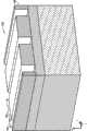
图13和图14说明可与鳍片行142的侧壁相抵而形成的牺牲材料146(其在此实施例中充当模具且可被称作模具)。牺牲材料142可通过侧壁隔片工艺而形成。牺牲材料142可由可在随后参考图18描述的行列传导下变得可流动(例如,其可变成例如气体或液体等流体)的材料形成。抛弃式模具材料的实例包括碳和特定聚合物,其皆可通过将其与氧在熔炉中进行反应而作为气体从衬底110移除。共形薄膜可沉积于衬底110上,从而覆盖上部掺杂区112和下部掺杂区114,且随后经各向异性蚀刻。侧壁隔片蚀刻可移除下部掺杂区114的一部分以形成凹部148。凹部148可具有通常等于或小于1F、1/2F或1/4F的宽度150。如下文所解释,继续侧壁隔片蚀刻直到其形成凹部148为止被认为减少了通过模具146形成的栅极彼此短路的可能性。在此实施例中,牺牲材料146在上部掺杂区112的底部上方延伸且具有可小于或通常等于1F、1/2F或1/4F的宽度152。13 and 14 illustrate a sacrificial material 146 (which in this embodiment acts as a mold and may be referred to as a mold) that may be formed against the sidewalls of the row of
在形成牺牲材料146之后,可将电介质区154形成于牺牲材料146上,如由图15所说明。在一些实施例中,电介质区154可为通过例如原子层沉积(ALD)等低温工艺而沉积的氧化物。所说明的电介质154大体上或完全包封牺牲材料146且包括覆盖层156。After forming
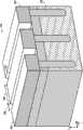
覆盖层156在图16所说明的平坦化步骤中被消耗。可通过回蚀、CMP或其它工艺对衬底110进行平坦化。在一些实施例中,可移除覆盖层156,直到暴露上部掺杂区112的顶部、深隔离沟槽118和浅沟槽130为止。电介质区154与这些结构112、118和130之间的转变可产生对用以对衬底110进行平坦化的工艺触发端点的现象。举例而言,此转变可得到衬底110的光学性质(例如,颜色)的改变、离开衬底110的废料的化学性质(例如,蚀刻室中的废气或浆料pH值)的改变,或衬底110的机械性质(例如,滑动摩擦)的改变。Capping layer 156 is consumed in the planarization step illustrated in FIG. 16 .
紧接着,如由图17所说明,可移除浅沟槽130中的材料的至少一部分。在一些实施例中,此材料为氮化物,且其是通过相对于硅和氧化物为选择性以避免损失这些材料的实质量的干式蚀刻而被移除。清除浅沟槽130的至少一部分会打开通向牺牲材料146的侧壁158的通路,且此通路可促进移除牺牲材料146。Next, at least a portion of the material in
如由图18所说明,可通过经由浅隔离沟槽130的打开通路而移除牺牲材料146。为了移除牺牲材料146,可将衬底110在(例如)等离子体蚀刻室中暴露于氧等离子体或在熔炉中暴露于氧。等离子体或其它反应物经由浅隔离沟槽130而流入,且(例如)通过燃烧牺牲材料146而与牺牲材料146的侧壁158进行反应。在一些实施例中,反应的副产物为气体,例如,蒸汽、一氧化碳和二氧化碳,且气体经由浅隔离沟槽130而回流出。在一些实施例中,继续燃烧,直到燃尽实质部分或大体上整个牺牲材料146且形成空腔160为止。所得空腔160在一侧上由电介质154界限且在另一侧上由鳍片行142界限。As illustrated by FIG. 18 ,
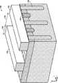
空腔160的形状由图19说明,图19说明在不具有衬底110的其它部分的情况下的空腔160。空腔160中的每一者可包括两个大体反射对称、大体线性且大体平行的空隙162和164以及多个沟槽区段166。所说明的沟槽区段166安置于空隙162和164的顶部部分中,且将空隙162与164彼此接合。邻近空腔160可通过电介质154(图18)而彼此大体上或全部地分离。The shape of
紧接着,如由图20所说明,可将栅极电介质166形成于空腔160内。栅极电介质166可(例如)通过CVD而沉积或通过将衬底110暴露于氧而生长。在所说明实施例中,栅极电介质166是通过将衬底110的硅部分与氧进行反应而生长,因此,栅极电介质166安置于鳍片行142的经暴露表面(包括浅沟槽130的表面)上。进行反应以形成栅极电介质166的氧或其它化学品经由沟槽区段166而流入至空腔160中,且与线性空隙162和164(图19)内的表面进行反应。在各种实施例中,栅极电介质166可由各种材料制成,包括氧化物、氮氧化物、铪基高k电介质,或其它适当材料。Next, as illustrated by FIG. 20 , a
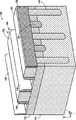
一旦形成栅极电介质166,便可将栅极材料沉积于空腔166内以形成栅极168,如由图21、图22和图23所说明。所说明的栅极168可通过沉积氮化钛或其它适当导电材料而形成。栅极材料可通过气相反应物而输送至衬底110且输送至空腔166中。反应物可经由浅沟槽130而流入至空腔166中且在空腔166的表面上进行反应。在一些实施例中,栅极材料在填充空腔166之前关闭浅沟槽130,借此留下空隙170。栅极材料的覆盖层可形成于衬底110的表面上,且覆盖层可通过湿式蚀刻、干式蚀刻或CMP工艺而被移除。Once
图24是通过上述工艺而形成的晶体管171的实例的分解透视图。然而,应注意,本技术不限于晶体管,且可用以形成例如电容器或浮动栅极晶体管等其它装置。所说明的晶体管171包括鳍片172、栅极电介质166和栅极168。所说明的鳍片172包括通过与浅沟槽130对应的大体U形狭槽178而分离的两个支柱174和176。鳍片172的远端部分由上部掺杂区112制成,且鳍片172的下部部分由下部掺杂区114制成。边缘180和182通常由深隔离沟槽118界定且可长于鳍片172的侧184和185。所说明的栅极166被安置成与侧184和185以及狭槽178的表面邻近。FIG. 24 is an exploded perspective view of an example of the transistor 171 formed through the above-described process. It should be noted, however, that the present technique is not limited to transistors, and may be used to form other devices such as capacitors or floating gate transistors. The illustrated transistor 171 includes a
在所说明实施例中,栅极168包括两个侧栅极186和188以及一顶部栅极190。两个侧栅极186和188为大体反射对称的且皆大体在X方向上延伸,其在一实质距离内具有大体均匀的横截面。除了空隙170之外,侧栅极186和188的形状与牺牲材料146的形状大体互补。所说明的顶部栅极190在Y方向上具有大体均匀的横截面且其将侧栅极186与188彼此接合。顶部栅极190可通常为实心、不具有空隙,或在一些实施例中,顶部栅极190也可包括空隙。侧栅极186被安置成与鳍片172的侧185至少部分地邻近,顶部栅极190被安置成至少部分地在狭槽178内,且侧栅极188被安置成与鳍片172的侧184至少部分地邻近。由于栅极168被安置成与鳍片172的两个侧和顶部部分邻近,因此所说明的晶体管171可被表征为三栅极晶体管。In the illustrated embodiment,
在操作中,两个支柱174和176可充当源极和漏极,且晶体管171可根据栅极168的电压而选择性地控制电流在源极与漏极之间的流动。所说明的晶体管171包括三个通道:由箭头192所表示的一大体水平通道,和由箭头194所表示的两个大体垂直通道。可通过从顶部栅极190发散的电场而建立大体水平通道192,且可通过从两个侧栅极186和188发散的电场而建立大体垂直通道194。In operation, the two
虽然本发明可易受各种修改和替代形式,但已在图式中通过实例而展示特定实施例且本文中已详细地描述特定实施例。然而,应理解,不希望本发明限于所揭示的特定形式。更确切而言,本发明将涵盖属于如由随附权利要求书所界定的本发明的精神和范围内的所有修改、均等物和替代物。While the invention is susceptible to various modifications and alternative forms, specific embodiments have been shown by way of example in the drawings and have been described herein in detail. It should be understood, however, that the invention is not intended to be limited to the particular forms disclosed. Rather, the invention is to cover all modifications, equivalents and alternatives falling within the spirit and scope of the invention as defined by the appended claims.
Claims (25)
Translated fromChineseApplications Claiming Priority (3)
| Application Number | Priority Date | Filing Date | Title |
|---|---|---|---|
| US12/043,813 | 2008-03-06 | ||
| US12/043,813US7915659B2 (en) | 2008-03-06 | 2008-03-06 | Devices with cavity-defined gates and methods of making the same |
| PCT/US2009/035018WO2009111225A1 (en) | 2008-03-06 | 2009-02-24 | Devices with cavity-defined gates and methods of making the same |
Publications (2)
| Publication Number | Publication Date |
|---|---|
| CN101960572A CN101960572A (en) | 2011-01-26 |
| CN101960572Btrue CN101960572B (en) | 2014-05-14 |
Family
ID=40551557
Family Applications (1)
| Application Number | Title | Priority Date | Filing Date |
|---|---|---|---|
| CN200980107635.9AActiveCN101960572B (en) | 2008-03-06 | 2009-02-24 | Devices with cavity-defined gates and methods of making same |
Country Status (6)
| Country | Link |
|---|---|
| US (3) | US7915659B2 (en) |
| JP (1) | JP5360507B2 (en) |
| KR (1) | KR101547375B1 (en) |
| CN (1) | CN101960572B (en) |
| TW (1) | TWI430371B (en) |
| WO (1) | WO2009111225A1 (en) |
Families Citing this family (36)
| Publication number | Priority date | Publication date | Assignee | Title |
|---|---|---|---|---|
| US7898857B2 (en) | 2008-03-20 | 2011-03-01 | Micron Technology, Inc. | Memory structure having volatile and non-volatile memory portions |
| US8546876B2 (en) | 2008-03-20 | 2013-10-01 | Micron Technology, Inc. | Systems and devices including multi-transistor cells and methods of using, making, and operating the same |
| US7969776B2 (en) | 2008-04-03 | 2011-06-28 | Micron Technology, Inc. | Data cells with drivers and methods of making and operating the same |
| KR20090105700A (en)* | 2008-04-03 | 2009-10-07 | 주식회사 하이닉스반도체 | Manufacturing method of semiconductor device |
| US8704375B2 (en)* | 2009-02-04 | 2014-04-22 | Taiwan Semiconductor Manufacturing Company, Ltd. | Barrier structures and methods for through substrate vias |
| JP5718585B2 (en)* | 2010-05-19 | 2015-05-13 | ピーエスフォー ルクスコ エスエイアールエルPS4 Luxco S.a.r.l. | Semiconductor device, manufacturing method thereof, and data processing system |
| DE102010030760B4 (en)* | 2010-06-30 | 2014-07-24 | Globalfoundries Dresden Module One Limited Liability Company & Co. Kg | Semiconductor device with via contacts with a stress relaxation mechanism and method of making the same |
| US8334196B2 (en) | 2010-11-01 | 2012-12-18 | Micron Technology, Inc. | Methods of forming conductive contacts in the fabrication of integrated circuitry |
| US9553193B2 (en) | 2010-11-19 | 2017-01-24 | Micron Technology, Inc. | Double gated fin transistors and methods of fabricating and operating the same |
| US8294511B2 (en) | 2010-11-19 | 2012-10-23 | Micron Technology, Inc. | Vertically stacked fin transistors and methods of fabricating and operating the same |
| US8293602B2 (en) | 2010-11-19 | 2012-10-23 | Micron Technology, Inc. | Method of fabricating a finFET having cross-hair cells |
| US8921899B2 (en) | 2010-11-19 | 2014-12-30 | Micron Technology, Inc. | Double gated 4F2 dram CHC cell and methods of fabricating the same |
| US8969154B2 (en)* | 2011-08-23 | 2015-03-03 | Micron Technology, Inc. | Methods for fabricating semiconductor device structures and arrays of vertical transistor devices |
| JP5646416B2 (en)* | 2011-09-01 | 2014-12-24 | 株式会社東芝 | Manufacturing method of semiconductor device |
| KR101823105B1 (en) | 2012-03-19 | 2018-01-30 | 삼성전자주식회사 | Method for fabricating field effect transistor |
| CN103531467B (en)* | 2012-07-02 | 2016-08-03 | 中芯国际集成电路制造(上海)有限公司 | Semiconductor device and forming method thereof |
| US9461143B2 (en) | 2012-09-19 | 2016-10-04 | Intel Corporation | Gate contact structure over active gate and method to fabricate same |
| US20140103452A1 (en)* | 2012-10-15 | 2014-04-17 | Marvell World Trade Ltd. | Isolation components for transistors formed on fin features of semiconductor substrates |
| US9263585B2 (en)* | 2012-10-30 | 2016-02-16 | Globalfoundries Inc. | Methods of forming enhanced mobility channel regions on 3D semiconductor devices, and devices comprising same |
| US8946050B2 (en)* | 2012-10-30 | 2015-02-03 | Globalfoundries Inc. | Double trench well formation in SRAM cells |
| CN103855026B (en)* | 2012-12-06 | 2017-04-19 | 中国科学院微电子研究所 | Finfet and manufacturing method thereof |
| CN103928334B (en)* | 2013-01-15 | 2017-06-16 | 中国科学院微电子研究所 | Semiconductor device and method for manufacturing the same |
| JP2014222682A (en)* | 2013-05-13 | 2014-11-27 | ピーエスフォー ルクスコ エスエイアールエルPS4 Luxco S.a.r.l. | Semiconductor device and method of manufacturing the same |
| US9343320B2 (en) | 2013-12-06 | 2016-05-17 | Globalfoundries Inc. | Pattern factor dependency alleviation for eDRAM and logic devices with disposable fill to ease deep trench integration with fins |
| US9871121B2 (en) | 2014-03-10 | 2018-01-16 | Qualcomm Incorporated | Semiconductor device having a gap defined therein |
| TWI642110B (en)* | 2014-12-03 | 2018-11-21 | 聯華電子股份有限公司 | Semiconductor component and manufacturing method thereof |
| US9466602B1 (en) | 2015-06-15 | 2016-10-11 | International Business Machines Corporation | Embedded dynamic random access memory field effect transistor device |
| US9553194B1 (en)* | 2015-07-29 | 2017-01-24 | Globalfoundries Inc. | Method for improved fin profile |
| CN106611787A (en)* | 2015-10-26 | 2017-05-03 | 联华电子股份有限公司 | Semiconductor structure and manufacturing method thereof |
| US10504821B2 (en)* | 2016-01-29 | 2019-12-10 | United Microelectronics Corp. | Through-silicon via structure |
| US9691864B1 (en)* | 2016-05-13 | 2017-06-27 | Infineon Technologies Americas Corp. | Semiconductor device having a cavity and method for manufacturing thereof |
| US10157745B2 (en)* | 2016-06-29 | 2018-12-18 | International Business Machines Corporation | High aspect ratio gates |
| US9934970B1 (en)* | 2017-01-11 | 2018-04-03 | International Business Machines Corporation | Self aligned pattern formation post spacer etchback in tight pitch configurations |
| US10770571B2 (en)* | 2018-09-19 | 2020-09-08 | Taiwan Semiconductor Manufacturing Co., Ltd. | FinFET with dummy fins and methods of making the same |
| US20220231023A1 (en)* | 2021-01-15 | 2022-07-21 | Taiwan Semiconductor Manufacturing Co., Ltd. | Finfet device and method |
| CN118738121A (en)* | 2024-04-15 | 2024-10-01 | 华南师范大学 | Based on multi-region gate single-channel microcavity transistor, optoelectronic full logic gate device, control method and circuit |
Citations (2)
| Publication number | Priority date | Publication date | Assignee | Title |
|---|---|---|---|---|
| US6605514B1 (en)* | 2002-07-31 | 2003-08-12 | Advanced Micro Devices, Inc. | Planar finFET patterning using amorphous carbon |
| CN101044615A (en)* | 2004-09-01 | 2007-09-26 | 微米技术有限公司 | DRAM cell with vertical U-shaped transistors |
Family Cites Families (106)
| Publication number | Priority date | Publication date | Assignee | Title |
|---|---|---|---|---|
| US3885861A (en) | 1972-10-02 | 1975-05-27 | Hughes Aircraft Co | Liquid crystal digital reticle |
| US5196910A (en) | 1987-04-24 | 1993-03-23 | Hitachi, Ltd. | Semiconductor memory device with recessed array region |
| US5160987A (en) | 1989-10-26 | 1992-11-03 | International Business Machines Corporation | Three-dimensional semiconductor structures formed from planar layers |
| US5109256A (en) | 1990-08-17 | 1992-04-28 | National Semiconductor Corporation | Schottky barrier diodes and Schottky barrier diode-clamped transistors and method of fabrication |
| KR930005234B1 (en) | 1990-09-13 | 1993-06-16 | 금성일렉트론주식회사 | Cell manufacture method of fin-stack cell |
| US6791131B1 (en) | 1993-04-02 | 2004-09-14 | Micron Technology, Inc. | Method for forming a storage cell capacitor compatible with high dielectric constant materials |
| US5864181A (en) | 1993-09-15 | 1999-01-26 | Micron Technology, Inc. | Bi-level digit line architecture for high density DRAMs |
| JPH07263576A (en) | 1994-03-25 | 1995-10-13 | Hitachi Ltd | Semiconductor integrated circuit device and manufacturing method thereof |
| US6831322B2 (en) | 1995-06-05 | 2004-12-14 | Fujitsu Limited | Semiconductor memory device and method for fabricating the same |
| JP3853406B2 (en) | 1995-10-27 | 2006-12-06 | エルピーダメモリ株式会社 | Semiconductor integrated circuit device and method for manufacturing the same |
| US6043562A (en) | 1996-01-26 | 2000-03-28 | Micron Technology, Inc. | Digit line architecture for dynamic memory |
| WO1997028532A1 (en) | 1996-02-01 | 1997-08-07 | Micron Technology, Inc. | Digit line architecture for dynamic memory |
| US5688709A (en) | 1996-02-14 | 1997-11-18 | Lsi Logic Corporation | Method for forming composite trench-fin capacitors for DRAMS |
| US5793033A (en) | 1996-03-29 | 1998-08-11 | Metanetics Corporation | Portable data collection device with viewing assembly |
| US7064376B2 (en) | 1996-05-24 | 2006-06-20 | Jeng-Jye Shau | High performance embedded semiconductor memory devices with multiple dimension first-level bit-lines |
| US5821513A (en) | 1996-06-26 | 1998-10-13 | Telxon Corporation | Shopping cart mounted portable data collection device with tethered dataform reader |
| US6285045B1 (en) | 1996-07-10 | 2001-09-04 | Fujitsu Limited | Semiconductor device with self-aligned contact and its manufacture |
| JP3941133B2 (en) | 1996-07-18 | 2007-07-04 | 富士通株式会社 | Semiconductor device and manufacturing method thereof |
| US6072209A (en) | 1997-07-08 | 2000-06-06 | Micro Technology, Inc. | Four F2 folded bit line DRAM cell structure having buried bit and word lines |
| US5925918A (en) | 1997-07-30 | 1999-07-20 | Micron, Technology, Inc. | Gate stack with improved sidewall integrity |
| US6097212A (en) | 1997-10-09 | 2000-08-01 | Lattice Semiconductor Corporation | Variable grain architecture for FPGA integrated circuits |
| US6130551A (en) | 1998-01-19 | 2000-10-10 | Vantis Corporation | Synthesis-friendly FPGA architecture with variable length and variable timing interconnect |
| US6137128A (en) | 1998-06-09 | 2000-10-24 | International Business Machines Corporation | Self-isolated and self-aligned 4F-square vertical fet-trench dram cells |
| US5858829A (en) | 1998-06-29 | 1999-01-12 | Vanguard International Semiconductor Corporation | Method for fabricating dynamic random access memory (DRAM) cells with minimum active cell areas using sidewall-spacer bit lines |
| TW388125B (en) | 1998-08-19 | 2000-04-21 | Vanguard Int Semiconduct Corp | Method for fabricating dynamic random access memory (DRAM) cells with minimum active cell areas |
| DE19842704C2 (en) | 1998-09-17 | 2002-03-28 | Infineon Technologies Ag | Manufacturing process for a capacitor with a high epsilon dielectric or a ferroelectric according to the fin stack principle using a negative mold |
| TW380316B (en) | 1998-10-15 | 2000-01-21 | Worldwide Semiconductor Mfg | Manufacturing method for fin-trench-structure capacitor of DRAM |
| US6100129A (en) | 1998-11-09 | 2000-08-08 | Worldwide Semiconductor Manufacturing Corporation | Method for making fin-trench structured DRAM capacitor |
| US6426175B2 (en) | 1999-02-22 | 2002-07-30 | International Business Machines Corporation | Fabrication of a high density long channel DRAM gate with or without a grooved gate |
| US6258559B1 (en)* | 1999-03-22 | 2001-07-10 | Zymogenetics, Inc. | Method for producing proteins in transformed Pichia |
| KR100325472B1 (en) | 1999-04-15 | 2002-03-04 | 박종섭 | Manufacturing Method of DRAM Memory Cells |
| JP4074051B2 (en) | 1999-08-31 | 2008-04-09 | 株式会社東芝 | Semiconductor substrate and manufacturing method thereof |
| US6282113B1 (en) | 1999-09-29 | 2001-08-28 | International Business Machines Corporation | Four F-squared gapless dual layer bitline DRAM array architecture |
| DE19946719A1 (en) | 1999-09-29 | 2001-04-19 | Infineon Technologies Ag | Trench capacitor used in the production of DRAM storage cells has a conducting contact layer between the substrate and the conducting trench filling in the trench above the insulating collar |
| JP3457236B2 (en) | 1999-11-05 | 2003-10-14 | 茂徳科技股▲ふん▼有限公司 | Method of manufacturing deep trench capacitor storage electrode |
| WO2001061738A1 (en) | 2000-02-15 | 2001-08-23 | Steag Cvd Systems Ltd. | Dram capacitor with ultra-thin nitride layer |
| US6391753B1 (en)* | 2000-06-20 | 2002-05-21 | Advanced Micro Devices, Inc. | Process for forming gate conductors |
| JP3983960B2 (en) | 2000-07-14 | 2007-09-26 | 株式会社ルネサステクノロジ | Manufacturing method of semiconductor integrated circuit device and semiconductor integrated circuit device |
| KR100466689B1 (en) | 2000-08-28 | 2005-01-24 | 인터내셔널 비지네스 머신즈 코포레이션 | Compact dual-port dram architecture system and method for making same |
| US6509226B1 (en) | 2000-09-27 | 2003-01-21 | International Business Machines Corporation | Process for protecting array top oxide |
| US6967147B1 (en) | 2000-11-16 | 2005-11-22 | Infineon Technologies Ag | Nitrogen implantation using a shadow effect to control gate oxide thickness in DRAM semiconductor |
| US6258659B1 (en) | 2000-11-29 | 2001-07-10 | International Business Machines Corporation | Embedded vertical DRAM cells and dual workfunction logic gates |
| US6576944B2 (en) | 2000-12-14 | 2003-06-10 | Infineon Technologies Ag | Self-aligned nitride pattern for improved process window |
| CA2340985A1 (en) | 2001-03-14 | 2002-09-14 | Atmos Corporation | Interleaved wordline architecture |
| US6809368B2 (en) | 2001-04-11 | 2004-10-26 | International Business Machines Corporation | TTO nitride liner for improved collar protection and TTO reliability |
| TW502453B (en)* | 2001-09-06 | 2002-09-11 | Winbond Electronics Corp | MOSFET and the manufacturing method thereof |
| US7190060B1 (en) | 2002-01-09 | 2007-03-13 | Bridge Semiconductor Corporation | Three-dimensional stacked semiconductor package device with bent and flat leads and method of making same |
| US7019353B2 (en) | 2002-07-26 | 2006-03-28 | Micron Technology, Inc. | Three dimensional flash cell |
| US6865100B2 (en) | 2002-08-12 | 2005-03-08 | Micron Technology, Inc. | 6F2 architecture ROM embedded DRAM |
| US7358121B2 (en)* | 2002-08-23 | 2008-04-15 | Intel Corporation | Tri-gate devices and methods of fabrication |
| US6927462B2 (en) | 2002-08-28 | 2005-08-09 | Infineon Technologes Richmond, Lp | Method of forming a gate contact in a semiconductor device |
| US6670682B1 (en) | 2002-08-29 | 2003-12-30 | Micron Technology, Inc. | Multilayered doped conductor |
| KR100481209B1 (en)* | 2002-10-01 | 2005-04-08 | 삼성전자주식회사 | MOS Transistor having multiple channels and method of manufacturing the same |
| DE10248722A1 (en) | 2002-10-18 | 2004-05-06 | Infineon Technologies Ag | Integrated circuit arrangement with capacitor and manufacturing process |
| JP3983167B2 (en)* | 2002-12-26 | 2007-09-26 | 華邦電子股▲ふん▼有限公司 | Method for manufacturing metal oxide semiconductor field effect transistor |
| DE10302128B3 (en) | 2003-01-21 | 2004-09-09 | Infineon Technologies Ag | Buffer amplifier system for buffer storage of signals runs several DRAM chips in parallel and has two output buffer amplifiers in parallel feeding reference and signal networks with capacitors and DRAMs |
| US6845033B2 (en) | 2003-03-05 | 2005-01-18 | International Business Machines Corporation | Structure and system-on-chip integration of a two-transistor and two-capacitor memory cell for trench technology |
| JP2004281782A (en) | 2003-03-17 | 2004-10-07 | Toshiba Corp | Semiconductor device and manufacturing method thereof |
| US6794254B1 (en) | 2003-05-15 | 2004-09-21 | Taiwan Semiconductor Manufacturing Company | Embedded dual-port DRAM process |
| US7099216B2 (en) | 2003-09-05 | 2006-08-29 | International Business Machines Corporation | Single cycle read/write/writeback pipeline, full-wordline I/O DRAM architecture with enhanced write and single ended sensing |
| US6844591B1 (en) | 2003-09-17 | 2005-01-18 | Micron Technology, Inc. | Method of forming DRAM access transistors |
| DE10361695B3 (en) | 2003-12-30 | 2005-02-03 | Infineon Technologies Ag | Transistor structure for dynamic random-access memory cell has recess structure between source/drain regions and vertical gate electrode enclosing active region on at least 2 sides |
| US6998666B2 (en) | 2004-01-09 | 2006-02-14 | International Business Machines Corporation | Nitrided STI liner oxide for reduced corner device impact on vertical device performance |
| DE102004006520B4 (en) | 2004-02-10 | 2010-05-12 | Qimonda Ag | Method for producing a DRAM memory cell arrangement with trench capacitors and ridge field effect transistors (FinFET) and DRAM memory cell arrangement |
| DE102004021052B3 (en) | 2004-04-29 | 2005-12-29 | Infineon Technologies Ag | Method for fabricating trench DRAM memory cells and trench DRAM memory cell array with curved channel bridge field effect transistors (CFET) |
| KR100605104B1 (en)* | 2004-05-04 | 2006-07-26 | 삼성전자주식회사 | Fin-Pet device and its manufacturing method |
| US7098105B2 (en) | 2004-05-26 | 2006-08-29 | Micron Technology, Inc. | Methods for forming semiconductor structures |
| JP4675585B2 (en)* | 2004-06-22 | 2011-04-27 | シャープ株式会社 | Field effect transistor |
| US7132333B2 (en) | 2004-09-10 | 2006-11-07 | Infineon Technologies Ag | Transistor, memory cell array and method of manufacturing a transistor |
| DE102004031385B4 (en) | 2004-06-29 | 2010-12-09 | Qimonda Ag | A method of fabricating ridge field effect transistors in a DRAM memory cell array, curved channel field effect transistors, and DRAM memory cell array |
| JP2006054431A (en) | 2004-06-29 | 2006-02-23 | Infineon Technologies Ag | Transistor, memory cell array, and transistor manufacturing method |
| DE102004043857B3 (en) | 2004-09-10 | 2006-03-30 | Infineon Technologies Ag | DRAM cell pair and DRAM memory cell array with stack and trench memory cells, and method of fabricating a DRAM memory cell array |
| DE102004043858A1 (en) | 2004-09-10 | 2006-03-16 | Infineon Technologies Ag | Method for producing a memory cell, a memory cell arrangement and memory cell arrangement |
| KR100585161B1 (en) | 2004-10-02 | 2006-05-30 | 삼성전자주식회사 | Multichannel transistor device manufacturing method and device |
| US7476920B2 (en) | 2004-12-15 | 2009-01-13 | Infineon Technologies Ag | 6F2 access transistor arrangement and semiconductor memory device |
| US7254074B2 (en) | 2005-03-07 | 2007-08-07 | Micron Technology, Inc. | Open digit line array architecture for a memory array |
| KR100691006B1 (en)* | 2005-04-29 | 2007-03-09 | 주식회사 하이닉스반도체 | Structure of Cell Transistor of Memory Device and Manufacturing Method Thereof |
| KR100608377B1 (en)* | 2005-05-02 | 2006-08-08 | 주식회사 하이닉스반도체 | Cell transistor manufacturing method of memory device |
| US7316953B2 (en) | 2005-05-31 | 2008-01-08 | Nanya Technology Corporation | Method for forming a recessed gate with word lines |
| KR100608380B1 (en) | 2005-06-01 | 2006-08-08 | 주식회사 하이닉스반도체 | Transistor of memory device and method for fabricating the same |
| US7282401B2 (en) | 2005-07-08 | 2007-10-16 | Micron Technology, Inc. | Method and apparatus for a self-aligned recessed access device (RAD) transistor gate |
| US7776715B2 (en) | 2005-07-26 | 2010-08-17 | Micron Technology, Inc. | Reverse construction memory cell |
| US7151023B1 (en) | 2005-08-01 | 2006-12-19 | International Business Machines Corporation | Metal gate MOSFET by full semiconductor metal alloy conversion |
| US20070058468A1 (en) | 2005-09-12 | 2007-03-15 | Promos Technologies Pte.Ltd. Singapore | Shielded bitline architecture for dynamic random access memory (DRAM) arrays |
| KR100663366B1 (en) | 2005-10-26 | 2007-01-02 | 삼성전자주식회사 | Flash memory device manufacturing method having self-aligned floating gate and related devices |
| KR100653712B1 (en) | 2005-11-14 | 2006-12-05 | 삼성전자주식회사 | Semiconductor devices in which an isolation layer having a top surface substantially the same as an active region in a fin FET is disposed and methods of forming the same |
| US7402856B2 (en) | 2005-12-09 | 2008-07-22 | Intel Corporation | Non-planar microelectronic device having isolation element to mitigate fringe effects and method to fabricate same |
| US8716772B2 (en) | 2005-12-28 | 2014-05-06 | Micron Technology, Inc. | DRAM cell design with folded digitline sense amplifier |
| KR100734304B1 (en) | 2006-01-16 | 2007-07-02 | 삼성전자주식회사 | Manufacturing method of transistor |
| KR100720238B1 (en) | 2006-01-23 | 2007-05-23 | 주식회사 하이닉스반도체 | Semiconductor element and manufacturing method thereof |
| US20070176253A1 (en) | 2006-01-31 | 2007-08-02 | Peng-Fei Wang | Transistor, memory cell and method of manufacturing a transistor |
| TWI294640B (en) | 2006-02-16 | 2008-03-11 | Nanya Technology Corp | Alignment mark and alignment method for the fabrication of trench-capacitor dram devices |
| JP2007294680A (en)* | 2006-04-25 | 2007-11-08 | Toshiba Corp | Semiconductor element, semiconductor device and manufacturing method thereof |
| US7573108B2 (en) | 2006-05-12 | 2009-08-11 | Micron Technology, Inc | Non-planar transistor and techniques for fabricating the same |
| KR100751803B1 (en)* | 2006-08-22 | 2007-08-23 | 삼성전자주식회사 | Manufacturing Method of Semiconductor Device |
| US7452766B2 (en)* | 2006-08-31 | 2008-11-18 | Micron Technology, Inc. | Finned memory cells and the fabrication thereof |
| US7776684B2 (en)* | 2007-03-30 | 2010-08-17 | Intel Corporation | Increasing the surface area of a memory cell capacitor |
| KR100942961B1 (en)* | 2007-10-24 | 2010-02-17 | 주식회사 하이닉스반도체 | Manufacturing method of semiconductor device having polysilicon gate electrode of columnar structure |
| US8866254B2 (en) | 2008-02-19 | 2014-10-21 | Micron Technology, Inc. | Devices including fin transistors robust to gate shorts and methods of making the same |
| US7742324B2 (en) | 2008-02-19 | 2010-06-22 | Micron Technology, Inc. | Systems and devices including local data lines and methods of using, making, and operating the same |
| US9190494B2 (en) | 2008-02-19 | 2015-11-17 | Micron Technology, Inc. | Systems and devices including fin field-effect transistors each having U-shaped semiconductor fin |
| US8546876B2 (en) | 2008-03-20 | 2013-10-01 | Micron Technology, Inc. | Systems and devices including multi-transistor cells and methods of using, making, and operating the same |
| US7808042B2 (en) | 2008-03-20 | 2010-10-05 | Micron Technology, Inc. | Systems and devices including multi-gate transistors and methods of using, making, and operating the same |
| US7898857B2 (en) | 2008-03-20 | 2011-03-01 | Micron Technology, Inc. | Memory structure having volatile and non-volatile memory portions |
| US7969776B2 (en) | 2008-04-03 | 2011-06-28 | Micron Technology, Inc. | Data cells with drivers and methods of making and operating the same |
| US8076229B2 (en) | 2008-05-30 | 2011-12-13 | Micron Technology, Inc. | Methods of forming data cells and connections to data cells |
- 2008
- 2008-03-06USUS12/043,813patent/US7915659B2/enactiveActive
- 2009
- 2009-02-24JPJP2010549726Apatent/JP5360507B2/enactiveActive
- 2009-02-24CNCN200980107635.9Apatent/CN101960572B/enactiveActive
- 2009-02-24KRKR1020107022401Apatent/KR101547375B1/enactiveActive
- 2009-02-24WOPCT/US2009/035018patent/WO2009111225A1/enactiveApplication Filing
- 2009-03-06TWTW098107482Apatent/TWI430371B/enactive
- 2011
- 2011-02-15USUS13/028,064patent/US8669159B2/enactiveActive
- 2014
- 2014-03-06USUS14/198,937patent/US9331203B2/enactiveActive
Patent Citations (2)
| Publication number | Priority date | Publication date | Assignee | Title |
|---|---|---|---|---|
| US6605514B1 (en)* | 2002-07-31 | 2003-08-12 | Advanced Micro Devices, Inc. | Planar finFET patterning using amorphous carbon |
| CN101044615A (en)* | 2004-09-01 | 2007-09-26 | 微米技术有限公司 | DRAM cell with vertical U-shaped transistors |
Also Published As
| Publication number | Publication date |
|---|---|
| KR20100131478A (en) | 2010-12-15 |
| US9331203B2 (en) | 2016-05-03 |
| JP5360507B2 (en) | 2013-12-04 |
| US7915659B2 (en) | 2011-03-29 |
| KR101547375B1 (en) | 2015-08-25 |
| US20090224357A1 (en) | 2009-09-10 |
| US20110143528A1 (en) | 2011-06-16 |
| JP2011514677A (en) | 2011-05-06 |
| US20140183626A1 (en) | 2014-07-03 |
| TW200947565A (en) | 2009-11-16 |
| CN101960572A (en) | 2011-01-26 |
| US8669159B2 (en) | 2014-03-11 |
| WO2009111225A1 (en) | 2009-09-11 |
| TWI430371B (en) | 2014-03-11 |
Similar Documents
| Publication | Publication Date | Title |
|---|---|---|
| CN101960572B (en) | Devices with cavity-defined gates and methods of making same | |
| US9087721B2 (en) | Devices including fin transistors robust to gate shorts and methods of making the same | |
| TWI481030B (en) | System and device with fin transistor and method of using, manufacturing and operating same | |
| CN101159233B (en) | Gate Etching Process for High Voltage Field Effect Transistors | |
| KR102612342B1 (en) | Liner structure in interlayer dielectric structure for semiconductor devices | |
| US10157748B2 (en) | Fin profile improvement for high performance transistor | |
| KR20200049614A (en) | Transistors with stacked semiconductor layers as channels | |
| KR100912960B1 (en) | Transistor having recess channel and manufacturing method thereof | |
| TW202345216A (en) | Semiconductor structure and method of forming the same |
Legal Events
| Date | Code | Title | Description |
|---|---|---|---|
| C06 | Publication | ||
| PB01 | Publication | ||
| C10 | Entry into substantive examination | ||
| SE01 | Entry into force of request for substantive examination | ||
| C14 | Grant of patent or utility model | ||
| GR01 | Patent grant |