CN101946313B - Probe wafer, probe device and test system - Google Patents
Probe wafer, probe device and test systemDownload PDFInfo
- Publication number
- CN101946313B CN101946313BCN2008801270994ACN200880127099ACN101946313BCN 101946313 BCN101946313 BCN 101946313BCN 2008801270994 ACN2008801270994 ACN 2008801270994ACN 200880127099 ACN200880127099 ACN 200880127099ACN 101946313 BCN101946313 BCN 101946313B
- Authority
- CN
- China
- Prior art keywords
- wafer
- probe
- splicing ear
- semiconductor chip
- semiconductor
- Prior art date
- Legal status (The legal status is an assumption and is not a legal conclusion. Google has not performed a legal analysis and makes no representation as to the accuracy of the status listed.)
- Expired - Fee Related
Links
Images


Classifications
- H—ELECTRICITY
- H01—ELECTRIC ELEMENTS
- H01L—SEMICONDUCTOR DEVICES NOT COVERED BY CLASS H10
- H01L22/00—Testing or measuring during manufacture or treatment; Reliability measurements, i.e. testing of parts without further processing to modify the parts as such; Structural arrangements therefor
- G—PHYSICS
- G01—MEASURING; TESTING
- G01R—MEASURING ELECTRIC VARIABLES; MEASURING MAGNETIC VARIABLES
- G01R1/00—Details of instruments or arrangements of the types included in groups G01R5/00 - G01R13/00 and G01R31/00
- G01R1/02—General constructional details
- G01R1/06—Measuring leads; Measuring probes
- G01R1/067—Measuring probes
- G01R1/073—Multiple probes
- G01R1/07307—Multiple probes with individual probe elements, e.g. needles, cantilever beams or bump contacts, fixed in relation to each other, e.g. bed of nails fixture or probe card
- G01R1/07364—Multiple probes with individual probe elements, e.g. needles, cantilever beams or bump contacts, fixed in relation to each other, e.g. bed of nails fixture or probe card with provisions for altering position, number or connection of probe tips; Adapting to differences in pitch
- G01R1/07378—Multiple probes with individual probe elements, e.g. needles, cantilever beams or bump contacts, fixed in relation to each other, e.g. bed of nails fixture or probe card with provisions for altering position, number or connection of probe tips; Adapting to differences in pitch using an intermediate adapter, e.g. space transformers
- G—PHYSICS
- G01—MEASURING; TESTING
- G01R—MEASURING ELECTRIC VARIABLES; MEASURING MAGNETIC VARIABLES
- G01R1/00—Details of instruments or arrangements of the types included in groups G01R5/00 - G01R13/00 and G01R31/00
- G01R1/02—General constructional details
- G01R1/06—Measuring leads; Measuring probes
- G01R1/067—Measuring probes
- G01R1/073—Multiple probes
- G—PHYSICS
- G01—MEASURING; TESTING
- G01R—MEASURING ELECTRIC VARIABLES; MEASURING MAGNETIC VARIABLES
- G01R31/00—Arrangements for testing electric properties; Arrangements for locating electric faults; Arrangements for electrical testing characterised by what is being tested not provided for elsewhere
- G01R31/28—Testing of electronic circuits, e.g. by signal tracer
- G01R31/282—Testing of electronic circuits specially adapted for particular applications not provided for elsewhere
- G01R31/2831—Testing of materials or semi-finished products, e.g. semiconductor wafers or substrates
Landscapes
- Engineering & Computer Science (AREA)
- Power Engineering (AREA)
- Physics & Mathematics (AREA)
- General Physics & Mathematics (AREA)
- Manufacturing & Machinery (AREA)
- Computer Hardware Design (AREA)
- Microelectronics & Electronic Packaging (AREA)
- Testing Or Measuring Of Semiconductors Or The Like (AREA)
- Testing Of Individual Semiconductor Devices (AREA)
- Measuring Leads Or Probes (AREA)
- Tests Of Electronic Circuits (AREA)
Abstract
Description
Translated fromChinese技术领域technical field
本发明涉及探针晶片、探针装置以及测试系统。本发明特别涉及与形成有多个半导体芯片的半导体晶片电连接的探针晶片。The invention relates to a probe wafer, a probe device and a testing system. In particular, the present invention relates to a probe wafer electrically connected to a semiconductor wafer on which a plurality of semiconductor chips are formed.
背景技术Background technique
在半导体芯片测试中,公知有一种装置可以在形成多个半导体芯片的半导体晶片状态,测试各半导体芯片的好坏(例如参考专利文献1)。该装置可认为是具有可与多个半导体芯片整体电连接的探针卡。In semiconductor chip testing, there is known a device that can test the quality of each semiconductor chip in the state of a semiconductor wafer on which a plurality of semiconductor chips are formed (for example, refer to Patent Document 1). This device can be considered as having a probe card integrally electrically connected to a plurality of semiconductor chips.
探针卡配置在测试装置的测试基板与半导体晶片之间。此处,在测试基板的端子排列间距与半导体晶片的端子排列间距相异时,可考虑使探针卡具有吸收该端子排列间距的功能。例如在该探针卡的表面及底面以不同间距配置端子,并与测试基板及半导体晶片电连接。如此可在探针卡内连接表面及底面相对应的端子。The probe card is disposed between the test substrate and the semiconductor wafer of the test device. Here, when the terminal arrangement pitch of the test substrate is different from that of the semiconductor wafer, it may be considered that the probe card has a function of absorbing the terminal arrangement pitch. For example, terminals are arranged at different pitches on the surface and bottom of the probe card, and are electrically connected to the test substrate and the semiconductor chip. In this way, the terminals corresponding to the surface and the bottom surface of the probe card can be connected.
专利文献1:日本专利特开2002-222839号公报Patent Document 1: Japanese Patent Laid-Open No. 2002-222839
专利文献2:国际公开专利第2003/062837号手册Patent Document 2: International Laid-Open Patent No. 2003/062837 Handbook
通常,使用印制电路板形成探针卡(例如参考专利文献2)。在该印制电路板形成多个探针销(probe pin),可与多个半导体芯片共同电连接。Generally, a printed circuit board is used to form a probe card (for example, refer to Patent Document 2). A plurality of probe pins are formed on the printed circuit board to be electrically connected to a plurality of semiconductor chips.
但是,因半导体晶片与印制电路板的热膨胀率不同,所以在测试时半导体芯片的发热、加热测试时或冷却测试等发生温度变动时,可以想象半导体芯片与探针卡之间的电连接有可能松开。此问题,对在大面积的半导体晶片上形成半导体芯片的测试时更为显着。However, since the thermal expansion coefficients of the semiconductor chip and the printed circuit board are different, it is conceivable that the electrical connection between the semiconductor chip and the probe card may be affected when the temperature of the semiconductor chip heats up during the test, or the temperature fluctuates during the heating test or the cooling test. May loosen. This problem is more remarkable in the case of testing semiconductor chips formed on a large-area semiconductor wafer.
发明内容Contents of the invention
为此,本发明的目的是提供一种能够解决上述问题的探针晶片、探针装置以及测试系统。此目的可由申请专利范围的各独立权项所述的特征的组合达成,而各从属权项规定本发明的更有利的具体例。Therefore, an object of the present invention is to provide a probe wafer, a probe device and a test system capable of solving the above problems. This object can be achieved by a combination of the features stated in the independent claims of the patent application, while the dependent claims specify more advantageous embodiments of the invention.
为了解决上述的问题,在本发明的第一方式提供一种与形成多个半导体芯片的半导体晶片电连接的探针晶片。该探针晶片包括:间距变换用晶片基板,具有晶片连接面及在晶片连接面的背面形成的装置连接面;多个晶片侧连接端子,在间距变换用晶片基板的晶片连接面上形成,对各个半导体芯片至少每一芯片设置一个,并与对应的半导体芯片的输入输出端子电连接;多个装置侧连接端子,在晶片基板的装置连接面与多个晶片侧连接端子一一对应,以与晶片侧连接端子不同的间距而形成,用于与外部的装置电连接;以及多个传输电路,用于将对应的晶片侧连接端子与装置侧连接端子电连接。In order to solve the above-mentioned problems, a first aspect of the present invention provides a probe wafer electrically connected to a semiconductor wafer on which a plurality of semiconductor chips are formed. The probe wafer includes: a wafer substrate for pitch conversion, which has a wafer connection surface and a device connection surface formed on the back surface of the wafer connection surface; a plurality of wafer side connection terminals are formed on the wafer connection surface of the pitch conversion wafer substrate. Each semiconductor chip is provided with at least one chip, and is electrically connected to the input and output terminals of the corresponding semiconductor chip; a plurality of device-side connection terminals are in one-to-one correspondence with a plurality of chip-side connection terminals on the device connection surface of the wafer substrate, so as to be connected with The chip-side connection terminals are formed with different pitches for electrical connection with external devices; and a plurality of transmission circuits are used for electrically connecting the corresponding chip-side connection terminals with the device-side connection terminals.
本发明的第二方式提供一种与形成多个半导体芯片的半导体晶片电连接的探针装置,其具有与半导体晶片电连接的间距变换用探针晶片,以及与该间距变换用探针晶片电连接的电路形成用探针晶片。该间距变换用探针晶片包括:间距变换用晶片基板,及多个晶片侧连接端子,其形成于该间距变换用晶片基板的与半导体晶片相对的面,对各个半导体芯片至少每一芯片设置一个,与对应的半导体芯片的输入输出端子电连接;及多个第一中间连接端子,在间距变换用晶片基板的与电路形成用探针晶片相对的面,与多个晶片侧连接端子一一对应,以和晶片侧连接端子不同的间距而形成,并与电路形成用探针晶片电连接;以及多个传输电路,用于电连接相对应的晶片侧连接端子与第一中间连接端子。上述的电路形成用探针晶片包括:电路形成用晶片基板,配置在与间距变换用晶片基板的形成多个第一中间连接端子的面的对面;及多个第二中间连接端子,在电路形成用晶片基板上形成,与多个第一中间连接端子一一对应设置,并与对应的第一中间连接端子电连接;以及多个电路部,对各个半导体芯片至少每一芯片设置一个,生成供给对应的半导体芯片的信号,并通过中间连接端子及晶片侧连接端子,向对应的半导体芯片供给信号。A second aspect of the present invention provides a probe device electrically connected to a semiconductor wafer on which a plurality of semiconductor chips are formed, comprising a pitch changing probe wafer electrically connected to the semiconductor wafer, and electrically connected to the pitch changing probe wafer. Connected circuits are formed using a probe wafer. The probe wafer for pitch conversion includes: a wafer substrate for pitch conversion, and a plurality of wafer-side connection terminals formed on the surface of the wafer substrate for pitch conversion opposite to the semiconductor wafer, and at least one is provided for each semiconductor chip. , are electrically connected to the input and output terminals of the corresponding semiconductor chips; and a plurality of first intermediate connection terminals correspond one-to-one to a plurality of wafer side connection terminals on the surface of the pitch conversion wafer substrate opposite to the circuit forming probe wafer , formed at different pitches from the wafer-side connection terminals and electrically connected to the circuit-forming probe wafer; and a plurality of transmission circuits for electrically connecting the corresponding wafer-side connection terminals with the first intermediate connection terminals. The above-mentioned probe wafer for circuit formation includes: a wafer substrate for circuit formation disposed opposite to the surface of the wafer substrate for pitch conversion on which a plurality of first intermediate connection terminals are formed; and a plurality of second intermediate connection terminals for circuit formation. Formed on a wafer substrate, provided in one-to-one correspondence with a plurality of first intermediate connection terminals, and electrically connected to the corresponding first intermediate connection terminals; and a plurality of circuit parts, at least one for each semiconductor chip, generating a supply The signal of the corresponding semiconductor chip is connected, and the signal is supplied to the corresponding semiconductor chip through the intermediate connection terminal and the wafer side connection terminal.
本发明的第三方式提供一种测试系统,对在半导体晶片上形成的多个半导体芯片进行测试。该测试系统包括:信号生成部,输出供给各半导体芯片的测试信号;及探针晶片,将自信号生成部接收的测试信号分别供给各半导体芯片;以及判定部,通过探针晶片接收各半导体芯片对应测试信号输出的响应信号,并根据该响应信号判定各半导体芯片的好坏。上述探针晶片包括:间距变换用晶片基板,具有晶片连接面及在该晶片连接面的背面形成的装置连接面;及多个晶片侧连接端子,形成于间距变换用晶片基板的晶片连接面,对应各半导体芯片至少每一芯片设置一个,与对应的半导体芯片的输入输出端子电连接;及多个装置侧连接端子,在晶片基板的装置连接面,与多个晶片侧连接端子一一对应,但以与晶片侧连接端子不同的间距而形成,与信号生成部电连接;以及多个传输电路,用于将对应的晶片侧连接端子与装置侧连接端子电连接。A third aspect of the present invention provides a test system for testing a plurality of semiconductor chips formed on a semiconductor wafer. The test system includes: a signal generation unit that outputs a test signal supplied to each semiconductor chip; and a probe wafer that supplies the test signal received from the signal generation unit to each semiconductor chip; and a determination unit that receives each semiconductor chip through the probe wafer. A response signal is output corresponding to the test signal, and the quality of each semiconductor chip is judged according to the response signal. The above-mentioned probe wafer includes: a wafer substrate for pitch conversion, which has a wafer connection surface and a device connection surface formed on the back surface of the wafer connection surface; and a plurality of wafer-side connection terminals formed on the wafer connection surface of the pitch conversion wafer substrate, Corresponding to each semiconductor chip, at least one is provided for each chip, and is electrically connected to the input and output terminals of the corresponding semiconductor chip; and a plurality of device-side connection terminals are in one-to-one correspondence with the plurality of chip-side connection terminals on the device connection surface of the wafer substrate, but formed at different pitches from the wafer-side connection terminals, electrically connected to the signal generation section; and a plurality of transmission circuits for electrically connecting the corresponding wafer-side connection terminals to the device-side connection terminals.
本发明的第四方式提供一种半导体测试系统,对在半导体晶片上形成的多个半导体芯片进行测试。该测试系统包括:信号生成部,输出供给各半导体芯片的测试信号,及探针装置,将自信号生成部接收的测试信号供给各半导体芯片,以及判定部,通过探针装置接收各半导体芯片回应测试信号输出的响应信号,并根据该响应信号判定各半导体芯片的好坏。上述探针装置包括:间距变换用探针晶片,与半导体晶片电连接,以及电路形成用探针晶片,与间距变换用探针晶片电连接。该间距变换用探针晶片还包括:间距变换用晶片基板;及多个晶片侧连接端子,形成于间距变换用晶片基板的与半导体晶片相对的面,对各半导体芯片至少每一芯片设置一个,与对应的半导体芯片的输入输出端子电连接;及多个第一中间连接端子,在间距变换用晶片基板的与电路形成用探针晶片相对的面,与多个晶片侧连接端子一一对应,以和晶片侧连接端子不同的间距而形成,而且与电路形成用探针晶片电连接;以及多个传输电路,用于电连接相对应的晶片侧连接端子与第一中间连接端子。上述电路形成用探针晶片包括:电路形成用晶片基板,配置在间距变换用晶片基板的具有多个第一中间连接端子的面的对面;及多个第二中间连接端子,在电路形成用晶片基板上形成,并与多个第一中间连接端子一一对应设置,与对应的第一中间连接端子电连接;以及多个电路部,对各半导体片至少每一芯片设置一个,通过中间连接端子及晶片侧连接端子测试对应的半导体芯片。A fourth aspect of the present invention provides a semiconductor test system for testing a plurality of semiconductor chips formed on a semiconductor wafer. The test system includes: a signal generation unit that outputs a test signal supplied to each semiconductor chip, and a probe device that supplies the test signal received from the signal generation unit to each semiconductor chip, and a determination unit that receives a response from each semiconductor chip through the probe device. The response signal output by the test signal is used to determine whether each semiconductor chip is good or bad according to the response signal. The above-mentioned probe device includes: a pitch changing probe wafer electrically connected to the semiconductor wafer, and a circuit forming probe wafer electrically connected to the pitch changing probe wafer. The probe wafer for pitch conversion further includes: a wafer substrate for pitch conversion; and a plurality of wafer-side connection terminals formed on a surface of the pitch conversion wafer substrate opposite to the semiconductor wafer, at least one for each semiconductor chip, Electrically connected to the input and output terminals of the corresponding semiconductor chip; and a plurality of first intermediate connection terminals corresponding to a plurality of wafer side connection terminals on the surface of the pitch conversion wafer substrate opposite to the circuit forming probe wafer, formed at different pitches from the wafer-side connection terminals and electrically connected to the circuit-forming probe wafer; and a plurality of transmission circuits for electrically connecting the corresponding wafer-side connection terminals and the first intermediate connection terminals. The above probe wafer for circuit formation includes: a wafer substrate for circuit formation disposed on the opposite surface of the wafer substrate for pitch conversion with a plurality of first intermediate connection terminals; and a plurality of second intermediate connection terminals disposed on the circuit formation wafer Formed on the substrate, and provided in one-to-one correspondence with a plurality of first intermediate connection terminals, and electrically connected to the corresponding first intermediate connection terminals; and a plurality of circuit parts, at least one for each chip of each semiconductor chip, through the intermediate connection terminals And the corresponding semiconductor chip is tested by the connecting terminal on the wafer side.
上述发明概要并未列举发明必要的全部特征,这些特征群的次级组合也可构成发明。The above-mentioned summary of the invention does not list all the necessary features of the invention, and sub-combinations of these feature groups may also constitute the invention.
附图说明Description of drawings
图1为一个实施例涉及的测试系统400的结构示意图。FIG. 1 is a schematic structural diagram of a
图2为一例探针晶片100的侧视图。FIG. 2 is a side view of an example of the
图3表示配有探针晶片100的探针装置200的剖面结构图。FIG. 3 shows a cross-sectional structural view of a
图4表示控制装置10的结构示意图。FIG. 4 shows a schematic structural view of the
图5表示探针晶片100的其它例的侧视图。FIG. 5 shows a side view of another example of
图6表示探针晶片100的其它的结构图。FIG. 6 shows another configuration diagram of the
图7表示测试系统400的其它结构示意图。FIG. 7 shows another structural schematic diagram of the
图8表示具有间距变换用探针晶片100-1及电路形成用探针晶片100-2的探针装置200的结构剖面图。FIG. 8 is a cross-sectional view showing the configuration of a
图9表示电路部110的结构示意图。FIG. 9 shows a schematic configuration diagram of the
图10表示测试电路120的功能的结构示意图。FIG. 10 shows a schematic configuration diagram of the function of the
图11表示测试电路120的其它结构示意图。FIG. 11 shows another structural schematic diagram of the
附图标记说明:Explanation of reference signs:
10 控制装置10 control device
12 主机12 Host
14 测试头14 test heads
100 探针晶片100 Probe Wafer
102 晶片连接面102 chip connection surface
104 装置连接面104 device connection surface
111 晶片基板111 chip substrate
112 晶片侧连接端子112 Chip side connection terminal
113 第一中间连接端子113 First intermediate connection terminal
114 装置侧连接端子114 Device side connection terminal
115 第二中间连接端子115 Second intermediate connection terminal
116 通孔116 through holes
117 配线117 Wiring
118 切换部118 Switching Department
119 垫片119 Gasket
120 测试电路120 test circuit
122 图案发生部122 Pattern Generation Department
124 图案存储器124 pattern memories
126 期待值存储器126 expected value memory
128 失效存储器128 failure memory
130 波形形成部130 Wave forming part
132 驱动器132 drives
134 比较器134 Comparators
136 时序发生部136 Sequence Generation Department
138 逻辑比较部138 Logic comparison department
140 特性检测部140 Characteristic Inspection Department
142 电源供给部142 Power Supply Unit
150 垫片150 spacers
160 开关160 switch
170 切换部170 switch unit
200 探针装置200 probe set
210 晶片托盘210 wafer tray
212 保持构件212 holding member
220 晶片侧隔板220 wafer side partition
222 凸块222 bump
230 晶片侧PCR230 wafer side PCR
240 装置侧PCR240 Device-side PCR
250 装置侧隔板250 unit side partitions
252 凸块252 bumps
260 装置基板260 device substrate
270 中间PCR270 Intermediate PCRs
280 中间隔板280 middle partition
282 凸块282 bumps
300 半导体晶片300 semiconductor wafers
310 半导体芯片310 semiconductor chip
400 测试系统400 test system
具体实施方式Detailed ways
下面通过发明的实施方式说明本发明,但以下实施方式并不限定权利要求所涉及的发明。另外,在实施方式中说明的特征组合并非全部都是发明的解决手段所必须的。Hereinafter, the present invention will be described through embodiments of the invention, but the following embodiments do not limit the invention according to the claims. In addition, not all combinations of features described in the embodiments are essential to the solution means of the invention.
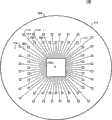
图1是一个实施例的测试系统400的结构示意图。测试系统400用于测试在测试对象半导体晶片300上形成的多个半导体芯片310,其包括探针晶片100以及控制装置10。另外,在图1中显示了半导体晶片300及探针晶片100的立体图的一例。FIG. 1 is a schematic structural diagram of a
半导体晶片300,可为例如圆盘状的半导体基板,更具体地说,半导体晶片300可为硅、化合物半导体或其它的半导体基板。另外,半导体芯片310,可在半导体晶片300上采用曝光等半导体工艺而形成。The
探针晶片100,用于电连接半导体晶片300与控制装置10。更具体地说,探针晶片100配置在控制装置10的各端子以及在半导体晶片300上形成的各端子之间,电连接控制装置10及半导体晶片300的相对应的端子。本例的探针晶片100,如后述的图2所示,包括间距变换用晶片基板111以及多个晶片侧连接端子112。The
控制装置10,通过探针晶片100测试半导体晶片300的各半导体芯片310。例如控制装置10,通过探针晶片100对各半导体芯片310供给测试信号。另外控制装置10可通过探针晶片100接收各半导体芯片310对应测试信号输出的响应信号,依据响应信号判定各半导体芯片310的好坏。The
图2是探针晶片100的侧视图的一例。如图1及图2所示,探针晶片100包括:间距变换用晶片基板111,晶片侧连接端子112,装置侧连接端子114,通孔116,垫片150以及配线117。FIG. 2 is an example of a side view of the
间距变换用晶片基板111,可用与半导体晶片300的基板相同的半导体材料形成。例如间距变换用晶片基板111,可用硅基板。另外,间距变换用晶片基板111,可用与半导体晶片300的基板具有大致相同热膨胀率的半导体材料形成。另外,间距变换用晶片基板111,如图2所示,具有晶片连接面102及在晶片连接面102的背面形成的装置连接面104。晶片连接面102,与图1所示的半导体晶片300相对形成。装置连接面104,与图1所示的控制装置10相对形成。The
另外,间距变换用晶片基板111,具有与半导体晶片300的形成半导体芯片310的面,以及大致相同形状的晶片连接面102。晶片连接面,可具有与半导体晶片的面直径大致相同的圆形。间距变换用晶片基板111,配置成其晶片连接面与半导体晶片300相对的方式。另外,间距变换用晶片基板111,也可为直径比半导体晶片300大的圆盘状的半导体基板。In addition, the
多个晶片侧连接端子112,形成于间距变换用晶片基板111的晶片连接面102。另外,晶片侧连接端子112,对各半导体芯片310至少每一芯片设置一个。例如晶片侧连接端子112,可针对各半导体芯片310的各个输入输出端子而分别设置。即,各半导体芯片310有多个输入输出端子时,晶片侧连接端子112,可对各半导体芯片310各设多个连接端。A plurality of wafer-
分别与半导体晶片300的各个输入输出端子以相同间隔设置各个晶片侧连接端子112,并与对应的半导体芯片310的输入输出端子电连接。另外所谓的电连接是指在两个构件间可传送电信号的状态。例如晶片侧连接端子112及半导体芯片310的输入输出端子可为直接接触,或经过其它的导体间接接触,以进行电连接。另外,晶片侧连接端子112及半导体芯片310的输入输出端子,可用如电容结合(静电结合)或感应结合(磁性结合)等,以非接触的状态电连接。另外晶片侧连接端子112及半导体芯片310的输入输出端子之间的传输线路的一部分,也可使用光学传输线路。The respective wafer-
多个装置侧连接端子114,形成于间距变换用晶片基板111的装置连接面104,与控制装置10电连接。装置侧连接端子114与多个晶片侧连接端子112一一对应设置。此处,装置侧连接端子114与控制装置10的端子以相同的间距设置。因此如图2所示,装置侧连接端子114可与晶片侧连接端子112以不同的间距设置。A plurality of device-
通孔116、垫片150及配线117在间距变换用晶片基板111上形成,使相对应的晶片侧连接端子112及装置侧连接端子114电连接。例如垫片150在装置连接面104上,设在与晶片侧连接端子112相对的位置。通孔116以一端连接晶片侧连接端子112,另一端与垫片150连接的方式,贯通间距变换用晶片基板111而形成。另外,配线117在装置连接面104上,电连接垫片150及装置侧连接端子114。通过上述的结构,能够电连接排列间距不同的装置侧连接端子114及晶片侧连接端子112。Via
例如,可使晶片侧连接端子112,为了与半导体芯片310的各输入端子电连接,与各输入端子以相同的间距配置。因此,晶片侧连接端子112,例如图1所示,可在每一半导体芯片310的预先决定的区域,以微小的间隔设置。For example, the wafer-
对此,各个装置侧连接端子114,可以比对应一个半导体芯片310的多个晶片侧连接端子112的间距更大的间隔设置。例如装置侧连接端子114,可在装置连接面104内以分布大致均等的等间距进行配置。In contrast, the respective device-
本例的探针晶片100,其间距变换用晶片基板111采用与半导体晶片300相同的半导体材料形成。故即使在周围的温度变动的场合,亦能良好维持探针晶片100与半导体晶片300之间的电连接。因此,例如在进行半导体晶片300的加热测试时,也能够精度良好地测试半导体晶片300。In the
另外,因间距变换用晶片基板111为用半导体材料形成,能够容易地在间距变换用晶片基板111上形成多个晶片侧连接端子112等。例如可使用曝光等的半导体工艺,容易地形成晶片侧连接端子112、装置侧连接端子114、通孔116以及配线117。因此,可将对应多个半导体芯片310的多个晶片侧连接端子112等,很容易地在间距变换用晶片基板111上形成。另外,探针晶片100的端子可利用导电材料的电镀、蒸镀等在间距变换用晶片基板111上形成。In addition, since the pitch
以上说明了探针晶片100在测试系统400中的使用例,但探针晶片100的用途不限于测试系统400。例如在半导体晶片300中形成多个半导体芯片310的状态,且该多个半导体芯片310用于电器等时,探针晶片100也可安装于相应的电器,与半导体晶片300电连接。The use example of the
图3表示配有探针晶片100的探针装置200结构的剖面图。本例利用探针装置200的各构成要件相分离的图进行说明,但探针装置200的各构成要件,在图3的上下方向与相邻的其它构成要件接触配置。本探针装置200用于保持半导体晶片300,使探针晶片100与半导体晶片300电连接。FIG. 3 shows a cross-sectional view of the structure of the
探针装置200包括:晶片托盘210、晶片侧隔板220、晶片侧PCR230、探针晶片100、装置侧PCR240、装置侧隔板250以及装置基板260。晶片托盘210用于保持半导体晶片300,例如晶片托盘210配置于半导体晶片300的无端子面312的对面。另外,晶片托盘210配有保持半导体晶片300的保持构件212。The
保持构件212,为将半导体晶片300夹持于晶片托盘210的挟持构件。另外保持构件212亦可以将半导体晶片300吸附于晶片托盘210,此时,在晶片托盘210形成贯通孔,保持构件212通过该贯通孔将半导体晶片300吸附于晶片托盘210。The holding
晶片侧隔板220配置在半导体晶片300及晶片侧PCR230之间,用于电连接半导体晶片300与晶片侧PCR230。晶片侧隔板220上设有贯通绝缘材料形成的薄板的表面与底面的多个导电体凸块222。凸块222与半导体晶片300的各半导体芯片310的各端子电连接,凸块222可以与探针晶片100的晶片侧连接端子112相同的配置设置。The wafer-
晶片侧PCR230,配置在晶片侧隔板220与探针晶片100之间,用于电连接晶片侧隔板220的凸块222与探针晶片100的晶片侧连接端子112。晶片侧PCR230为利用凸块222及晶片侧连接端子112按压从而电连接凸块222及晶片侧连接端子112的,可使用异向性导电膜形成的薄板。Wafer-
装置侧PCR240,配置在探针晶片100与装置侧隔板250之间,用于电连接探针晶片100的装置侧连接端子114与装置侧隔板250的凸块252。装置侧PCR240,为利用装置侧连接端子114及凸块252的按压而电连接装置侧连接端子114及凸块252的,可使用异向性导电膜形成的薄板。The device-
装置侧隔板250,配置在装置侧PCR240与装置基板260之间,用于电连接装置侧PCR240与装置基板260。装置侧隔板250上设有贯通绝缘材料形成的薄板的表面与底面的多个导电体的凸块252。凸块252与装置基板260的各端子电连接。凸块252可用与探针晶片100的装置侧连接端子114相同的配置设置。The device-
装置基板260可用于固定由晶片托盘210起至装置侧隔板250之间的构件。例如可利用螺丝钉或真空吸附等固定由晶片托盘210至装置基板260之间的构件。另外装置基板260可电连接控制装置10与装置侧隔板250的各凸块252。装置基板260可为印制电路板。The
此外,各个隔板在通过隔板电连接的端子(垫片)的面积较小,或端子为铝膜等而在其表面形成氧化膜的情况下也有效。因此,在通过隔板电连接的端子的面积充分大时,省略隔板亦可。例如装置基板260的端子为大面积而容易进行镀金,故探针装置200也可以不设置装置侧隔板250。In addition, each spacer is also effective when the area of the terminal (pad) electrically connected through the spacer is small, or the terminal is formed of an aluminum film or the like and an oxide film is formed on the surface thereof. Therefore, when the area of the terminal electrically connected via the spacer is sufficiently large, the spacer may be omitted. For example, the terminal of the
根据上述的结构,可使探针晶片100与半导体晶片300电连接,又可使探针晶片100与控制装置10电连接。再者优选晶片侧隔板220,用与半导体晶片300的基板具有同等热膨胀率的材料形成。另外,装置侧隔板250,最好使用与间距变换用晶片基板111具有同等膨胀率的材料形成。According to the above configuration, the
图4是控制装置10的结构示意图。控制装置10包括主机12及测试头14。主机12用于控制测试头14测试半导体晶片300的各个半导体芯片310。测试头14回应由主机12的控制而产生测试信号,并经过探针装置200供给各个半导体芯片310。例如,测试头14可对各半导体芯片310供给相同的测试信号。FIG. 4 is a schematic structural diagram of the
另外,测试头14通过探针装置200接收各个半导体芯片310的响应信号。测试头14可依据各响应信号来判断各半导体芯片310的好坏。测试头14可将各个半导体芯片310的好坏判定结果,传送到主机12。根据这样的结构,能够进行进半导体芯片310的测试。In addition, the test head 14 receives the response signal of each
此外,在图4中所示的为主机12与测试头14分开的装置,但主机12与测试头14可为一体的装置。例如控制装置10包括的测试设备少的场合,可将主机12及测试头14容纳于一个筐体内。In addition, what is shown in FIG. 4 is a device in which the host 12 and the test head 14 are separated, but the host 12 and the test head 14 may be an integrated device. For example, when the
图5表示探针晶片100的其它例的侧视图。本例的探针晶片100,在图2所说明的探针晶片100的构造中再加设开关160。FIG. 5 shows a side view of another example of
开关160,设在垫片150与装置侧连接端子114之间,用于切换垫片150及装置侧连接端子114是否经过配线117连接。开关160,可借助于在半导体工艺形成的晶体管切换该连接。The
开关160,可对全部装置侧连接端子114设置,也可只对一部分装置侧连接端子114设置。通过这样的构造,可对半导体芯片310的每个管脚分别切换,确定控制装置10与半导体芯片310是否电连接。The
另外,装置侧连接端子114的至少一个,可用于接受从控制装置10应供给半导体芯片310的电源电力。例如,每个半导体芯片310至少有一个装置侧输入端子114,从控制装置10接受电源电力。所述装置侧连接端子114对应的晶片侧连接端子112,通过通孔116接受电源电力,向对应的半导体芯片310供给电源电力。In addition, at least one of the device-
此外,在接受电源电力的装置侧连接端子114对应的通孔116上,可填充与其它传送信号的通孔116不同的导电材料。例如传送电源电力的通孔116,因不需高精度传送高频率的信号,故可填充比其它通孔116的填充材料高频特性低的导电材料。例如可在传送电源电力的通孔116上填充铜,其它的通孔116上填充金。In addition, the through-
图6上探针晶片100的其它构造图。图6中示出了探针晶片100的装置连接面104。本例的探针晶片100为在图2所说明的探针晶片100的构造之外,再加设切换部170。Other structural diagrams of the
切换部170,用于切换各装置侧连接端子114与任一垫片150连接。例如切换部170通过配线117连接各个装置侧连接端子114及各个垫片150。然后,可将对应于各个装置侧连接端子114的配线117,切换至与某一个垫片150对应的配线117电连接。例如,切换部170可利用多个晶体管切换所述配线117的连接。The
还有图6中示出了用一个切换部170控制全部配线117的连接例。但其它例也可用多个切换部170控制配线117的连接。例如,将探针晶片100依规定的区域分割,各个切换部170控制其对应的区域内的配线117的连接亦可。多个切换部170对应多个半导体芯片310而设置,各个切换部170进行与各半导体芯片310对应的晶片侧连接端子112和装置侧连接端子114的连接的切换。Also, FIG. 6 shows a connection example in which all
另外,垫片150、配线117以及切换部170可配置在晶片连接面102上。此时,通孔116一端连接装置侧连接端子114,另一端连接到垫片150。另外,配线117将各个垫片150及各个晶片侧连接端子112连接到切换部170。切换部170对各个垫片150是否连接某一个晶片侧连接端子112进行切换。In addition, the
通常,对于连接多个装置侧连接端子114的控制装置10的多个测试模块,依其功能而决定配置于测试头14的某一槽口。例如作为电源供给模块的测试模块,为连接半导体芯片310的电源管脚对应的装置侧连接端子114,配置在该装置侧连接端子114对应的槽口上。Usually, a plurality of test modules of the
与此相反,本例的探针晶片100能够变更多个装置侧连接端子114与多个晶片侧连接端子112的连接关系。因此,能够将配置在任意槽口的各个测试模块,由切换部170的设定变更连接到半导体芯片310的规定的端子312。即,本例的测试系统400可以提高测试头14的设计的自由度。In contrast, in the
图7是测试系统400的其它结构的示意图。本例的测试系统400包括:间距变换用探针晶片100-1,电路形成用探针晶片100-2,以及控制装置10。探针晶片100-1配置在半导体晶片300与探针晶片100-2之间。另外探针晶片100-2,配置在探针晶片100-1及控制装置10之间。各个探针晶片100-1及探针晶片100-2,可形成与半导体晶片300的形成半导体芯片310的面大致相同直径的圆形面。FIG. 7 is a schematic diagram of other structures of the
探针晶片100-1,可具有与图1至图6所说明的探针晶片100相同的功能与构造。惟在探针晶片100-1的装置连接面104上形成多个第一中间连接端子以取代多个装置侧连接端子114,并经过第一中间连接端子与探针晶片100-2电连接。第一中间连接端子的构造可与装置侧连接端子114相同。The probe wafer 100-1 may have the same function and structure as the
探针晶片100-2包括:电路形成用晶片基板111-2,多个电路部110,多个第二中间连接端子115以及多个装置侧连接端子。晶片基板111-2可用与探针晶片100-1的间距变换用基板111-1相同的材料形成。The probe wafer 100-2 includes a wafer substrate 111-2 for circuit formation, a plurality of
多个第二中间连接端子115,在晶片基板111-2的与探针晶片100-1相对的面上形成。多个第二中间连接端子115,与探针晶片100-1的第一中间连接端子一一对应设置,分别与对应的第一中间连接端子电连接。探针晶片100-2经过第二中间连接端子115与探针晶片100-1交接信号。A plurality of second
多个装置侧连接端子,与图1至图6所说明的装置侧连接端子114同样地与控制装置10电连接。各个装置侧连接端经过通孔等与对应的第二中间连接端子115电连接。The plurality of device-side connection terminals are electrically connected to the
电路部110,对各个半导体芯片310至少每一芯片设置一个。各个电路部110,在晶片基板111-2上形成,通过第二中间连接端子115及探针晶片100-1与对应的半导体芯片310交接信号。另外,各个电路部110通过装置侧连接端子与控制装置10交接信号。At least one
各个电路部110,可发生测试对应的半导体芯片310的测试信号并供给半导体芯片310。另外,各个电路部110,可以接收对应的半导体芯片310输出的响应信号。各个电路部110,可借助于对各响应信号的逻辑图案与预定的期待值图案进行比较,而判定各半导体芯片310的好坏。Each
各个电路部110,可具有图4所示的主机12及测试头14的全部功能或部分功能。通过上述结构可减低控制装置10的规模。例如控制装置10,只要具有对电路部110通知测试开始等时序的功能,将电路部110的测试结果读出的功能,以及向电路部110和半导体芯片310供给驱动电力的功能等各功能即可。Each
另外因晶片基板111-2用半导体材料制成,所以可容易地在晶片基板111-2形成高密度的电路部110。例如可利用曝光等半导体工艺,能够容易地在晶片基板111上形成高密度的电路部110。因此,可在晶片基板111上容易地形成对应于多个半导体芯片的多个电路部110。In addition, since the wafer substrate 111-2 is made of a semiconductor material, a high-
如以上说明,本例测试系统400能够降低因温度变动等引起的端子间的接触不良。另外能够降低测试系统400的规模。因设有间距变换用探针晶片100-1及电路形成用探针晶片100-2,例如在进行测试内容相同但端子间距不同的半导体晶片300的测试时,可以共同使用电路形成用探针晶片100-2,只要更换间距变换用探针晶片100-1即可,能够减少测试成本。As described above, the
图8是具有间距变换用探针晶片100-1及电路形成用探针晶片100-2的探针装置200的构造剖面图。本例中用探针装置200的各构成要件互相分离的图进行了说明,但探针装置200的各构成要件,在图8的上下方向与相邻的其它构成要件接触配置。8 is a cross-sectional view showing the structure of a
探针装置200包括:晶片托盘210、晶片侧隔板220、晶片侧PCR230、探针晶片100、装置侧PCR240、装置侧隔板250、中间PCR270、中间隔板280以及装置基板260。晶片托盘210用于保持半导体晶片300。The
其中的晶片托盘210、晶片侧隔板220以及晶片侧PCR230,可与图3所说明的晶片托盘210、晶片侧隔板220以及晶片侧PCR具有相同的功能及结构。另外,晶片侧PCR230配置在晶片侧隔板220与探针晶片100-1之间,用于电连接晶片侧隔板220的凸块222与探针晶片100-1的晶片侧连接端子112。The
另外,探针晶片100-1在与中间PCR270相对的面上,设有多个第一中间连接端子113。各个第一中间连接端子113,与图2所说明的装置侧连接端子114同样地经过通孔116与对应的晶片侧连接端子112电连接。另外,多个第一中间连接端子113,设置成与后述的第二中间连接端子115相同的配置。另外,第一中间连接端子113可以设置成与晶片侧连接端子112不同的配置。In addition, the probe wafer 100 - 1 is provided with a plurality of first
中间PCR270配置在探针晶片100-1与中间隔板280之间,用于电连接探针晶片100-1的第一中间连接端子113与中间隔板280的凸块282。中间PCR270可为由第一中间连接端子113及凸块282按压而电连接第一中间连接端子113及凸块282的,可使用异向性导电膜形成的薄板。The
中间隔板280配置在中间PCR270与探针晶片100-2之间,用于电连接中间PCR270与探针晶片100-2。中间隔板280上设有贯通用绝缘材料形成的薄板表面与底面的多个导电体凸块282。凸块282与探针晶片100-2的第二中间连接端子115电连接。凸块282可设置成与探针晶片100-2的第二中间连接端子115相同的配置。The
另外,探针晶片100-2,在晶片基板111-2的与中间隔板280对应的面上,设有与多个第一中间连接端子113一一对应的多个第二中间连接端子115。各个第二中间连接端子115,经由贯通晶片基板112的通孔,电连接到对应的装置侧连接端子114。第二中间连接端子115,可与装置侧连接端子114设置为相同的配置。In addition, the probe wafer 100-2 is provided with a plurality of second
装置侧PCR240、装置侧隔板250及装置基板260,可具有与图3所说明的装置侧PCR240、装置侧隔板250及装置基板260相同的功能及构造。另外,装置侧PCR240配置在探针晶片100-2与装置侧隔板250之间,用于电连接探针晶片100-2与装置侧隔板250。通过这样的构造,可利用两个探针晶片100测试半导体晶片300。The device-
另外,如图3所述,本例的探针装置200也可省略任一个隔板。例如与图3已说明的实施例同样地,探针装置200可不设置装置侧隔板250。又因探针晶片100的端子为大面积且比较容易用镀金等方法形成,故探针装置200可以不设中间隔板280。In addition, as shown in FIG. 3 , the
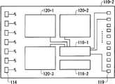
图9表示电路部110的构造示意图。在本例中,以电路部110形成于晶片基板111-2的与控制装置10相对的面为例加以说明。另外,在晶片基板111-2上形成的多个电路部110,每一个可具有相同的构造。FIG. 9 shows a schematic configuration diagram of the
各个电路部110,设有多个测试电路120及多个切换部118。又在电路部110中设有多个垫片119。多个垫片119,如图7及图8所述经过通孔与第二中间连接端子115电连接。Each
各个测试电路120可经过装置侧连接端子114连接到控制装置10。各个测试电路120可由控制部10供给控制信号、电源电力等。另外,平常时由第一测试电路120-1工作,其它的测试电路120在第一测试电路故障时工作。多个测试电路120,各个可以为相同的电路。Each
各个切换部118从多个测试电路120中,选择正在动作的测试电路120。在平常时,由第一切换部118-1工作,其它的切换部118在第一切换部118-1故障时工作。多个切换部118,各个可为相同的电路。切换部118,使选择的测试电路120经过垫片119连接第二中间连接端子115,以测试对应的半导体芯片310。Each switching unit 118 selects an
如上所述,因电路部110在半导体晶片基板111上形成,故能够高密度地形成含有半导体组件的测试电路120。因此,能够容易地在半导体芯片310的对应区域内,设置已含预备电路的多个测试电路120。另外电路部110可为含有一个测试电路120而不具有切换部118的结构。As described above, since the
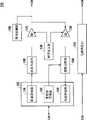
图10是测试电路120的功能构成示意图。测试电路120包括:图案发生部122、波形形成部130、驱动器132、比较器134、时序发生部136、逻辑比较部138、特性检测部140以及电源供给部142。又测试电路120,可在每一个连接的半导体芯片310的输入输出管脚的管脚,设有如图5所示的构造。FIG. 10 is a schematic diagram of the functional configuration of the
图案发生部122,发生测试信号的逻辑图案。本例的图案发生部122包括图案存储器124、期待值存储器126以及失效存储器128。图案发生部122,可将预先储存于图案存储器124的逻辑图案输出。图案存储器124,可储存在测试开始前由控制装置10供给的逻辑图案。另外,图案发生部122可依据预先给予的演算方法,生成该逻辑图案。The
波形形成部130,依据图案发生部122供给的逻辑图案,形成测试信号的波形。例如波形形成部130可将对应于逻辑图案的各逻辑值的电压,在各个规定的间隔期间输出以形成测试信号的波形。The
驱动器132,将从波形形成部130供给的波形所对应的测试信号输出。驱动器132,可回应由时序发生部136供给的时序信号,而输出测试信号。例如驱动器132可输出与时序信号相同周期的测试信号。驱动器132输出的测试信号,经过切换部118等而供给对应的半导体芯片310。The
比较器134,用于检测半导体芯片310输出的响应信号。例如比较器134可对应由时序发生部136供给的选通信号,而依次检测出响应信号的逻辑值,以检测响应信号的逻辑图案。The
逻辑比较部138,依据比较器134检测的响应信号的逻辑值,而判定对应的半导体芯片310的好坏,具有判定部的功能。例如,逻辑比较部138可依据由图案发生部122供给的期待值图案,与比较器134检测的逻辑值图案是否一致,判断半导体芯片310的好坏。图案发生部122,可将预先储存于期待值存储器126的期待值图案,供给逻辑比较部138。期待值存储器126,可储存在测试开始前由控制装置10供给的逻辑图案。另外,图案发生部122,也可依据预先供给的演算方法生成该期待值图案。The
失效存储器128,用于储存由逻辑比较部138比较的比较结果。例如在测试半导体芯片310的存储区域时,失效存储器128,可储存逻辑比较部138对半导体芯片310的每一地址的好坏判定结果。控制装置10可以读出在失效存储器128储存的好坏判定结果,例如,装置侧连接端子114可将失效存储器128储存的好坏判定结果,输出到探针晶片100-2外部的控制装置10。The
特性检测部140用于检测驱动器132输出的电压或电流的波形。例如,特性检测部140,可依据由驱动器132供给半导体芯片310的电流或电压的波形是否满足规定的规格而判定半导体芯片310好坏,即具有作为判定部的功能。The
电源供给部142,供给驱动半导体芯片310的电源电力,例如电源供给部142,可在测试中将对应于由控制装置10供给的电力的电源电力,供给半导体芯片310。另外,电源供应部142也可对测试电路120的各构成要件供给驱动电力。The
测试电路120因具有上述的构造,故能实现降低了控制装置10的规模的测试系统400。例如,作为控制装置10可使用一般的个人电脑等。Since the
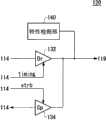
图11表示测试电路120的其它构造示意图。本例的测试电路120,具有图10中说明的测试电路120的结构中的一部分。例如本例的测试电路120可具备驱动器132、比较器134、以及特性检测部140。驱动器132、比较器134以及特性检测部140,可与图10中说明的驱动器132、比较器134以及特性检测部140相同。FIG. 11 shows a schematic diagram of another configuration of the
在这种情况下,控制部10可包括在图10中说明的图案发生部122、波形形成部130、时序发生部136、逻辑比较部138以及电源供给部142。测试电路120回应由控制装置10供给的控制信号而输出测试信号。另外,测试电路120,将比较器134的检测结果传送到控制装置10。依本例的测试电路120的结构,能够降低控制装置10的规模。In this case, the
另外,探针晶片100,可对规定个数的半导体芯片310的每一个设置一个电路部110。在此种情况下,各个电路部110可以测试从对应的多个半导体芯片310之中选出的任何一个半导体芯片310。In addition, in the
以上,通过实施方式说明了本发明,但以上实施方式并不限定权利要求所涉及的发明。另外,本领域技术人员明白,能够对上述实施例加以多种多样的改良和变更。根据权利要求的记载可以明确,实施了这样的变更和改良的实施方式也包含在本发明的技术范围之内。As mentioned above, although this invention was demonstrated based on embodiment, the said embodiment does not limit the invention which concerns on a claim. In addition, it is clear to those skilled in the art that various improvements and changes can be added to the above-described embodiments. It is clear from the description of the claims that embodiments including such changes and improvements are also included in the technical scope of the present invention.
Claims (10)
Applications Claiming Priority (1)
| Application Number | Priority Date | Filing Date | Title |
|---|---|---|---|
| PCT/JP2008/055790WO2009118850A1 (en) | 2008-03-26 | 2008-03-26 | Probe wafer, probe device, and testing system |
Publications (2)
| Publication Number | Publication Date |
|---|---|
| CN101946313A CN101946313A (en) | 2011-01-12 |
| CN101946313Btrue CN101946313B (en) | 2012-09-26 |
Family
ID=41113091
Family Applications (1)
| Application Number | Title | Priority Date | Filing Date |
|---|---|---|---|
| CN2008801270994AExpired - Fee RelatedCN101946313B (en) | 2008-03-26 | 2008-03-26 | Probe wafer, probe device and test system |
Country Status (7)
| Country | Link |
|---|---|
| US (1) | US8134379B2 (en) |
| EP (1) | EP2259297A1 (en) |
| JP (1) | JP5306326B2 (en) |
| KR (2) | KR101265974B1 (en) |
| CN (1) | CN101946313B (en) |
| TW (1) | TWI401446B (en) |
| WO (1) | WO2009118850A1 (en) |
Families Citing this family (8)
| Publication number | Priority date | Publication date | Assignee | Title |
|---|---|---|---|---|
| TWI455222B (en)* | 2011-08-25 | 2014-10-01 | Chipmos Technologies Inc | Testing method for stacked semiconductor device structure |
| JP5492230B2 (en)* | 2012-01-20 | 2014-05-14 | 株式会社日本マイクロニクス | Inspection device |
| US9391447B2 (en) | 2012-03-06 | 2016-07-12 | Intel Corporation | Interposer to regulate current for wafer test tooling |
| CN103018501B (en)* | 2012-12-11 | 2014-12-10 | 江苏汇成光电有限公司 | Wafer test probe card |
| KR102179245B1 (en)* | 2014-03-19 | 2020-11-16 | 주식회사 아도반테스토 | Wafer for inspection and test system |
| US20200292578A1 (en)* | 2017-08-03 | 2020-09-17 | FemtoDx | Wafer level probing of electrical biosensors |
| US10877089B2 (en)* | 2018-09-24 | 2020-12-29 | Taiwan Semiconductor Manufacturing Co., Ltd. | Semiconductor wafer testing system and related method for improving external magnetic field wafer testing |
| CN112444727A (en)* | 2019-08-28 | 2021-03-05 | 飞锃半导体(上海)有限公司 | Wafer testing system and method |
Citations (2)
| Publication number | Priority date | Publication date | Assignee | Title |
|---|---|---|---|---|
| US6229329B1 (en)* | 1997-09-04 | 2001-05-08 | Matsushita Electric Industrial Co., Ltd. | Method of testing electrical characteristics of multiple semiconductor integrated circuits simultaneously |
| CN101065681A (en)* | 2004-10-15 | 2007-10-31 | 泰拉丁公司 | Interface apparatus for semiconductor device tester |
Family Cites Families (12)
| Publication number | Priority date | Publication date | Assignee | Title |
|---|---|---|---|---|
| JPH11274252A (en)* | 1998-03-19 | 1999-10-08 | Mitsubishi Electric Corp | Semiconductor device inspection apparatus and inspection method |
| US6420884B1 (en) | 1999-01-29 | 2002-07-16 | Advantest Corp. | Contact structure formed by photolithography process |
| US6535003B2 (en) | 1999-01-29 | 2003-03-18 | Advantest, Corp. | Contact structure having silicon finger contactor |
| US6917525B2 (en)* | 2001-11-27 | 2005-07-12 | Nanonexus, Inc. | Construction structures and manufacturing processes for probe card assemblies and packages having wafer level springs |
| JP2001021587A (en) | 1999-07-08 | 2001-01-26 | Nec Corp | Inspection probe and its manufacture |
| JP2001210685A (en)* | 1999-11-19 | 2001-08-03 | Hitachi Ltd | Test system and method of manufacturing semiconductor integrated circuit device |
| JP2002222839A (en) | 2001-01-29 | 2002-08-09 | Advantest Corp | Probe card |
| WO2003062837A1 (en) | 2002-01-25 | 2003-07-31 | Advantest Corporation | Probe card and method for manufacturing probe card |
| JP2004170314A (en) | 2002-11-21 | 2004-06-17 | Advantest Corp | Testing device, testing method, and electric current measuring instrument |
| JP2004288911A (en) | 2003-03-24 | 2004-10-14 | Casio Comput Co Ltd | Semiconductor wafer test apparatus and test method therefor |
| JP2005079144A (en)* | 2003-08-28 | 2005-03-24 | Kyocera Corp | Multilayer wiring board and probe card |
| KR100712561B1 (en)* | 2006-08-23 | 2007-05-02 | 삼성전자주식회사 | Wafer type probe card, manufacturing method thereof and semiconductor inspection device provided with wafer type probe card |
- 2008
- 2008-03-26CNCN2008801270994Apatent/CN101946313B/ennot_activeExpired - Fee Related
- 2008-03-26KRKR1020127022714Apatent/KR101265974B1/ennot_activeExpired - Fee Related
- 2008-03-26KRKR1020107014592Apatent/KR101265973B1/ennot_activeExpired - Fee Related
- 2008-03-26WOPCT/JP2008/055790patent/WO2009118850A1/enactiveApplication Filing
- 2008-03-26JPJP2010505091Apatent/JP5306326B2/ennot_activeExpired - Fee Related
- 2008-03-26EPEP08738957Apatent/EP2259297A1/ennot_activeWithdrawn
- 2009
- 2009-03-17TWTW098108617Apatent/TWI401446B/ennot_activeIP Right Cessation
- 2010
- 2010-08-16USUS12/857,478patent/US8134379B2/ennot_activeExpired - Fee Related
Patent Citations (2)
| Publication number | Priority date | Publication date | Assignee | Title |
|---|---|---|---|---|
| US6229329B1 (en)* | 1997-09-04 | 2001-05-08 | Matsushita Electric Industrial Co., Ltd. | Method of testing electrical characteristics of multiple semiconductor integrated circuits simultaneously |
| CN101065681A (en)* | 2004-10-15 | 2007-10-31 | 泰拉丁公司 | Interface apparatus for semiconductor device tester |
Non-Patent Citations (2)
| Title |
|---|
| JP特开2000-249722A 2000.09.14 |
| JP特开2005-79144A 2005.03.24 |
Also Published As
| Publication number | Publication date |
|---|---|
| US20110109337A1 (en) | 2011-05-12 |
| KR101265974B1 (en) | 2013-05-22 |
| KR20120112847A (en) | 2012-10-11 |
| CN101946313A (en) | 2011-01-12 |
| EP2259297A1 (en) | 2010-12-08 |
| KR20100090718A (en) | 2010-08-16 |
| TWI401446B (en) | 2013-07-11 |
| WO2009118850A1 (en) | 2009-10-01 |
| JP5306326B2 (en) | 2013-10-02 |
| JPWO2009118850A1 (en) | 2011-07-21 |
| TW200944815A (en) | 2009-11-01 |
| KR101265973B1 (en) | 2013-05-22 |
| US8134379B2 (en) | 2012-03-13 |
Similar Documents
| Publication | Publication Date | Title |
|---|---|---|
| CN101946313B (en) | Probe wafer, probe device and test system | |
| KR101204109B1 (en) | Probe wafer, probe device, and testing system | |
| US7436199B2 (en) | Stack-type semiconductor package sockets and stack-type semiconductor package test systems | |
| US7541680B2 (en) | Semiconductor device package | |
| JP5269897B2 (en) | Test system and test board unit | |
| JP5588347B2 (en) | Probe apparatus and test apparatus | |
| CN104465436B (en) | Substrate check device | |
| US7372286B2 (en) | Modular probe card | |
| TWI389234B (en) | Testing wafer unit and test system | |
| JP5461394B2 (en) | Test wafer unit and test system | |
| US20130169302A1 (en) | System and adapter for testing packaged integrated circuit chips | |
| JPH04262551A (en) | Wafer testing method and semiconductor device tested thereby | |
| JPH09252031A (en) | Wafer tester | |
| KR102840197B1 (en) | Probe card having power conversion unit and test system including the same | |
| JPH07318587A (en) | Probe card | |
| KR20110005287A (en) | Test wafers, test systems, and semiconductor wafers |
Legal Events
| Date | Code | Title | Description |
|---|---|---|---|
| C06 | Publication | ||
| PB01 | Publication | ||
| C10 | Entry into substantive examination | ||
| SE01 | Entry into force of request for substantive examination | ||
| C14 | Grant of patent or utility model | ||
| GR01 | Patent grant | ||
| C17 | Cessation of patent right | ||
| CF01 | Termination of patent right due to non-payment of annual fee | Granted publication date:20120926 Termination date:20140326 |