CN101930147A - Electrophoretic display device - Google Patents
Electrophoretic display deviceDownload PDFInfo
- Publication number
- CN101930147A CN101930147ACN2010102163861ACN201010216386ACN101930147ACN 101930147 ACN101930147 ACN 101930147ACN 2010102163861 ACN2010102163861 ACN 2010102163861ACN 201010216386 ACN201010216386 ACN 201010216386ACN 101930147 ACN101930147 ACN 101930147A
- Authority
- CN
- China
- Prior art keywords
- substrate
- display device
- electrophoretic display
- particles
- thin film
- Prior art date
- Legal status (The legal status is an assumption and is not a legal conclusion. Google has not performed a legal analysis and makes no representation as to the accuracy of the status listed.)
- Granted
Links
Images


Classifications
- G—PHYSICS
- G02—OPTICS
- G02F—OPTICAL DEVICES OR ARRANGEMENTS FOR THE CONTROL OF LIGHT BY MODIFICATION OF THE OPTICAL PROPERTIES OF THE MEDIA OF THE ELEMENTS INVOLVED THEREIN; NON-LINEAR OPTICS; FREQUENCY-CHANGING OF LIGHT; OPTICAL LOGIC ELEMENTS; OPTICAL ANALOGUE/DIGITAL CONVERTERS
- G02F1/00—Devices or arrangements for the control of the intensity, colour, phase, polarisation or direction of light arriving from an independent light source, e.g. switching, gating or modulating; Non-linear optics
- G02F1/01—Devices or arrangements for the control of the intensity, colour, phase, polarisation or direction of light arriving from an independent light source, e.g. switching, gating or modulating; Non-linear optics for the control of the intensity, phase, polarisation or colour
- G02F1/165—Devices or arrangements for the control of the intensity, colour, phase, polarisation or direction of light arriving from an independent light source, e.g. switching, gating or modulating; Non-linear optics for the control of the intensity, phase, polarisation or colour based on translational movement of particles in a fluid under the influence of an applied field
- G02F1/1675—Constructional details
- G—PHYSICS
- G02—OPTICS
- G02F—OPTICAL DEVICES OR ARRANGEMENTS FOR THE CONTROL OF LIGHT BY MODIFICATION OF THE OPTICAL PROPERTIES OF THE MEDIA OF THE ELEMENTS INVOLVED THEREIN; NON-LINEAR OPTICS; FREQUENCY-CHANGING OF LIGHT; OPTICAL LOGIC ELEMENTS; OPTICAL ANALOGUE/DIGITAL CONVERTERS
- G02F1/00—Devices or arrangements for the control of the intensity, colour, phase, polarisation or direction of light arriving from an independent light source, e.g. switching, gating or modulating; Non-linear optics
- G02F1/01—Devices or arrangements for the control of the intensity, colour, phase, polarisation or direction of light arriving from an independent light source, e.g. switching, gating or modulating; Non-linear optics for the control of the intensity, phase, polarisation or colour
- G02F1/165—Devices or arrangements for the control of the intensity, colour, phase, polarisation or direction of light arriving from an independent light source, e.g. switching, gating or modulating; Non-linear optics for the control of the intensity, phase, polarisation or colour based on translational movement of particles in a fluid under the influence of an applied field
- G02F1/166—Devices or arrangements for the control of the intensity, colour, phase, polarisation or direction of light arriving from an independent light source, e.g. switching, gating or modulating; Non-linear optics for the control of the intensity, phase, polarisation or colour based on translational movement of particles in a fluid under the influence of an applied field characterised by the electro-optical or magneto-optical effect
- G02F1/167—Devices or arrangements for the control of the intensity, colour, phase, polarisation or direction of light arriving from an independent light source, e.g. switching, gating or modulating; Non-linear optics for the control of the intensity, phase, polarisation or colour based on translational movement of particles in a fluid under the influence of an applied field characterised by the electro-optical or magneto-optical effect by electrophoresis
- H—ELECTRICITY
- H10—SEMICONDUCTOR DEVICES; ELECTRIC SOLID-STATE DEVICES NOT OTHERWISE PROVIDED FOR
- H10D—INORGANIC ELECTRIC SEMICONDUCTOR DEVICES
- H10D86/00—Integrated devices formed in or on insulating or conducting substrates, e.g. formed in silicon-on-insulator [SOI] substrates or on stainless steel or glass substrates
- H10D86/40—Integrated devices formed in or on insulating or conducting substrates, e.g. formed in silicon-on-insulator [SOI] substrates or on stainless steel or glass substrates characterised by multiple TFTs
- H10D86/441—Interconnections, e.g. scanning lines
- H—ELECTRICITY
- H10—SEMICONDUCTOR DEVICES; ELECTRIC SOLID-STATE DEVICES NOT OTHERWISE PROVIDED FOR
- H10D—INORGANIC ELECTRIC SEMICONDUCTOR DEVICES
- H10D86/00—Integrated devices formed in or on insulating or conducting substrates, e.g. formed in silicon-on-insulator [SOI] substrates or on stainless steel or glass substrates
- H10D86/40—Integrated devices formed in or on insulating or conducting substrates, e.g. formed in silicon-on-insulator [SOI] substrates or on stainless steel or glass substrates characterised by multiple TFTs
- H10D86/60—Integrated devices formed in or on insulating or conducting substrates, e.g. formed in silicon-on-insulator [SOI] substrates or on stainless steel or glass substrates characterised by multiple TFTs wherein the TFTs are in active matrices
Landscapes
- Physics & Mathematics (AREA)
- Nonlinear Science (AREA)
- General Physics & Mathematics (AREA)
- Optics & Photonics (AREA)
- Health & Medical Sciences (AREA)
- Life Sciences & Earth Sciences (AREA)
- Chemical & Material Sciences (AREA)
- Chemical Kinetics & Catalysis (AREA)
- Electrochemistry (AREA)
- Molecular Biology (AREA)
- Electrochromic Elements, Electrophoresis, Or Variable Reflection Or Absorption Elements (AREA)
Abstract
Translated fromChinese
Description
Translated fromChinese相关申请的交叉引用Cross References to Related Applications
本申请基于2009年6月24日提出的日本专利申请第2009-149357号以及2009年6月24日提出的日本专利申请第2009-149359号,并主张其优先权,这里引用该日本专利申请的全部内容。This application is based on Japanese Patent Application No. 2009-149357 filed on June 24, 2009 and Japanese Patent Application No. 2009-149359 filed on June 24, 2009, and claims its priority. The Japanese patent application is cited here all content.
技术领域technical field
本发明涉及电泳显示装置。The present invention relates to electrophoretic display devices.
背景技术Background technique
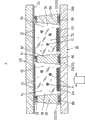
以往,作为电泳显示装置,已知有使用了微隔壁结构的电泳方式的电泳显示装置。这种电泳显示装置100例如图10所示,设有构成显示面的对置基板101以及与对置基板101对置配置的薄膜晶体管基板102。在薄膜晶体管基板102中的与对置基板101对置的内面设有:以矩阵状排列的多个像素电极103;以及信号线(扫描线、数据线)104,包围像素电极103的周围并经由未图示的薄膜晶体管与该像素电极103电连接。各信号线104形成有朝向对置基板101立设的、截面大致为梯形状的隔壁105,通过该隔壁105,各像素电极103的上侧区域从相邻的像素电极103的上侧区域隔开。Conventionally, as an electrophoretic display device, an electrophoretic display device using a micro-barrier rib structure is known. Such an
另一方面,在对置基板101的与薄膜晶体管基板102对置的内面,设有与多个像素电极103对置排列的对置电极106。On the other hand, on the inner surface of the
在由这些对置基板101、薄膜晶体管基板102以及隔壁105形成的空间内填充有溶媒107。在溶媒107中分散有多个带正电的黑粒子108以及带负电的白粒子109。A
并且,若将对置电极106的电压设为比像素电极103高,则白粒子109向对置电极106侧移动,并且黑粒子108向像素电极103侧移动,从而在显示面上显示白色(例如,图10所示的状态)。相反,若将对置电极106的电压设为比像素电极103小,则白粒子109向像素电极103侧移动,并且黑粒子108向对置电极106侧移动,从而在显示面上显示黑色。通过对每一个像素进行这些,在显示面上描绘规定的图形或文字。And, if the voltage of the
这里,在制造电泳显示装置100时,在薄膜晶体管基板102的内面,形成像素电极103、信号线104以及薄膜晶体管之后形成隔壁105。然后,在薄膜晶体管基板102的内面,流入分散了粒子108、109的溶媒107,并在其上叠加了形成有对置电极106的对置基板101。由于是这样的制造工序,因此制造上必然存在在隔壁103的上面残留粒子108、109的问题。若在隔壁103的上面残留着粒子108、109,则在像素间存在与想要显示的颜色相反的颜色的粒子(在图10中为黑粒子108a),因此成为使对比率下降的主要原因。Here, when the
发明内容Contents of the invention
因此,本发明的目的是提供一种抑制了对比率的下降的电泳显示装置。Therefore, an object of the present invention is to provide an electrophoretic display device in which a decrease in contrast ratio is suppressed.
本发明的电泳显示装置的一个方式是具备:One aspect of the electrophoretic display device of the present invention includes:
第一基板及第二基板,以预先设定的间隔对置配置;The first substrate and the second substrate are arranged facing each other at a preset interval;
多个像素电极,排列于上述第一基板;a plurality of pixel electrodes arranged on the first substrate;
布线,配置在相邻的上述像素电极之间;Wiring arranged between adjacent pixel electrodes;
对置电极,设置于上述第二基板;The opposite electrode is arranged on the above-mentioned second substrate;
隔壁,朝向上述第二基板而设置在上述第一基板的上述布线上,以包围上述多个像素电极;以及a partition wall disposed on the wiring of the first substrate facing the second substrate so as to surround the plurality of pixel electrodes; and
溶媒,填充在由上述隔壁包围的区域,并且分散有多个粒子。The solvent is filled in the region surrounded by the above-mentioned partition walls, and a plurality of particles are dispersed therein.
并且,在上述第一基板上,与上述隔壁对应地形成有防反射膜。Furthermore, an antireflection film is formed on the first substrate corresponding to the partition walls.
此外,在上述隔壁与上述防反射膜之间的层有形成有上述布线。Moreover, the said wiring is formed in the layer between the said partition wall and the said antireflection film.
本发明的电泳显示装置的其他方式是,具备:Another aspect of the electrophoretic display device of the present invention includes:
第一基板及第二基板,以预先设定的间隔对置配置;The first substrate and the second substrate are arranged facing each other at a preset interval;
第一电极,设置于上述第一基板;a first electrode disposed on the first substrate;
第二电极,设置于上述第二基板;The second electrode is arranged on the above-mentioned second substrate;
隔壁,配置在上述第一基板及上述第二基板之间,以包围第一电极的方式立设;以及The partition wall is arranged between the first substrate and the second substrate, and stands upright to surround the first electrode; and
溶媒,填充在被上述隔壁包围的区域,分散有多个粒子。The solvent is filled in the region surrounded by the above-mentioned partition walls, and a plurality of particles are dispersed therein.
并且,在上述第一基板上形成的上述隔壁的与上述第二基板对置的上述隔壁的面形成为凸状的曲面。In addition, a surface of the partition wall formed on the first substrate and facing the second substrate is formed as a convex curved surface.
根据本发明,能够提供抑制了对比率的下降的电泳显示装置。According to the present invention, it is possible to provide an electrophoretic display device in which a decrease in contrast ratio is suppressed.
本发明的其他特征和优点将在随后的说明中进行阐述,一部分可以通过说明书而明了,或者可以通过本发明的实践而体验到。通过说明书、权利要求书和附图中具体指出的结构,可以实现或获得本发明的这些和其它优点。Other features and advantages of the present invention will be set forth in the following description, some of them can be understood through the description, or can be experienced through the practice of the present invention. These and other advantages of the invention may be realized or attained by the structure particularly pointed out in the written description, claims hereof and the appended drawings.
附图说明Description of drawings
本发明所包括的附图也构成本说明书的一部分,对本发明的实施例进行阐明,并且和上面给出的总体描述及下面给出的对实施方案的详细说明一起,解释本发明的原理。The accompanying drawings included in the present invention also constitute a part of this specification, illustrate embodiments of the present invention, and together with the general description given above and the detailed description of the embodiments given below, explain the principle of the present invention.
图1是示意地表示第一实施方式的电泳显示装置的要部结构的截面图。FIG. 1 is a cross-sectional view schematically showing the configuration of main parts of an electrophoretic display device according to a first embodiment.
图2是表示图1的电泳显示装置所具备的薄膜晶体管基板的要部结构的截面图,是从图3的II-II切断线看的截面图。2 is a cross-sectional view showing the structure of a main part of a thin film transistor substrate included in the electrophoretic display device of FIG. 1 , and is a cross-sectional view viewed from line II-II in FIG. 3 .
图3是表示图1的电泳显示装置所具备的薄膜晶体管基板的要部结构的透射平面图。3 is a transmissive plan view showing the configuration of main parts of a thin film transistor substrate included in the electrophoretic display device of FIG. 1 .
图4A是在图1的薄膜晶体管基板形成的各层的形成方法的说明图,是在薄膜晶体管基板上形成了防反射膜的状态。4A is an explanatory diagram of a method of forming each layer formed on the thin film transistor substrate of FIG. 1 , showing a state in which an antireflection film is formed on the thin film transistor substrate.
图4B是在图1的薄膜晶体管基板形成的各层的形成方法的说明图,是形成了栅极、扫描线以及栅极布线的状态。FIG. 4B is an explanatory diagram of a method of forming each layer formed on the thin film transistor substrate of FIG. 1 , showing a state where gates, scanning lines, and gate wirings are formed.
图4C是在图1的薄膜晶体管基板形成的各层的形成方法的说明图,是形成了辅助容量线的状态。FIG. 4C is an explanatory diagram of a method of forming each layer formed on the thin film transistor substrate of FIG. 1 , showing a state in which auxiliary capacity lines are formed.
图4D是在图1的薄膜晶体管基板形成的各层的形成方法的说明图,是形成了栅极绝缘膜、本征非晶形硅及沟道保护膜的状态。4D is an explanatory diagram of a method of forming layers formed on the thin film transistor substrate of FIG. 1 , showing a state in which a gate insulating film, intrinsic amorphous silicon, and a channel protective film are formed.
图5A是在图1的薄膜晶体管基板形成的各层的形成方法的说明图,是形成了半导体薄膜、欧姆接触层、源极电极、漏极电极以及漏极膜,并形成了薄膜晶体管及数据线的状态。5A is an explanatory diagram of the formation method of each layer formed on the thin film transistor substrate of FIG. state of the line.
图5B是在图1的薄膜晶体管基板形成的各层的形成方法的说明图,是形成了外敷膜及接触孔的状态。5B is an explanatory diagram of a method of forming each layer formed on the thin film transistor substrate of FIG. 1 , showing a state where an overcoat film and a contact hole are formed.
图5C是在图1的薄膜晶体管基板形成的各层的形成方法的说明图,是形成了像素电极24的状态。FIG. 5C is an explanatory diagram of a method of forming each layer formed on the thin film transistor substrate of FIG. 1 , and shows a state where the
图6是表示用于形成图1的电泳显示装置所具有的隔壁的隔壁用膜的概略结构的分解斜视图。6 is an exploded perspective view showing a schematic structure of a barrier rib film for forming barrier ribs included in the electrophoretic display device of FIG. 1 .
图7是示意地表示第二实施方式的电泳显示装置的要部结构的截面图。7 is a cross-sectional view schematically showing the configuration of main parts of an electrophoretic display device according to a second embodiment.
图8是表示图7的电泳显示装置所具备的薄膜晶体管基板的要部结构的截面图,是从图3的II-II切断线看的截面图。8 is a cross-sectional view showing the structure of a main part of a thin film transistor substrate included in the electrophoretic display device of FIG. 7 , and is a cross-sectional view viewed from line II-II in FIG. 3 .
图9是示意地表示第二实施方式的电泳显示装置的变形例的截面图。9 is a cross-sectional view schematically showing a modified example of the electrophoretic display device of the second embodiment.
图10是示意地表示以往的电泳显示装置的要部结构的截面图。FIG. 10 is a cross-sectional view schematically showing the configuration of main parts of a conventional electrophoretic display device.
具体实施方式Detailed ways
以下,利用附图说明用于实施本发明的最优方式。其中,在以下所述的实施方式中虽然进行了用于实施本发明而在技术上优选的各种限定,但发明的范围不限定于以下的实施方式及图示例。Hereinafter, the best mode for carrying out the present invention will be described with reference to the drawings. In addition, in the embodiment described below, although various limitations technically preferable for carrying out the present invention are made, the scope of the invention is not limited to the following embodiment and illustrated examples.
[第一实施方式][first embodiment]
首先,参照附图说明本发明的第一实施方式。First, a first embodiment of the present invention will be described with reference to the drawings.
图1是示意地表示第一实施方式的电泳显示装置的要部结构的截面图。如该图1所示,在电泳显示装置1中设有对置基板10、通过隔壁60以与对置电极10之间的规定的间隔对置配置的薄膜晶体管基板20。该对置基板10为第二基板,薄膜晶体管基板20为第一基板。在薄膜晶体管基板20,以矩阵状形成有像素电极24,在像素电极之间形成有作为布线的扫描线22及数据线23。在扫描线22及数据线23上以格子状形成有隔壁60,在扫描线22及数据线23与薄膜晶体管基板20之间形成有防反射膜80。在对置基板10与薄膜晶体管基板20之间形成有未图示的框状的密封材料,并以隔壁60为间隔件,在一对基板之间形成了空间,在该空间内封入有分散了黑色粒子71与白色粒子72的溶媒70。FIG. 1 is a cross-sectional view schematically showing the configuration of main parts of an electrophoretic display device according to a first embodiment. As shown in FIG. 1 , an
对置基板10例如由玻璃形成。在对置基板10的与薄膜晶体管基板20对置的内面层叠有对置电极11。对置电极11例如由ITO(Indium Tin Oxide:氧化铟锡)形成。The
在溶媒70中分散有表面的极性和颜色不同的多个两种粒子。两种粒子中的一种是例如由碳构成的带正电的黑粒子71,另一种是例如由TiO2(氧化钛)构成的带负电的白粒子72。这里,黑粒子71的直径是5.0μm以下,白粒子72的直径是0.3μm以下。并且,作为溶媒70,使用介电常数比黑粒子71、白粒子72低的分散煤。In the solvent 70, a plurality of two types of particles having different surface polarities and colors are dispersed. One of the two kinds of particles is positively charged
下面,参照图2及图3对薄膜晶体管基板20进行详细的说明。图3是表示薄膜晶体管基板20的要部结构的透射平面图。另外,图2是图3中的II-II截面图。Next, the thin
首先,参照图3对薄膜晶体管基板20的平面结构进行说明。薄膜晶体管基板20由玻璃等形成,在其上面,多个扫描线22及多个数据线23相互交叉地形成。在该情况下,多个扫描线22在行方向上延伸而设置,多个数据线23在列方向上延伸而配置。First, the planar structure of the thin
在薄膜晶体管基板20上由扫描线22与数据线23包围的各区域内,设有一部分被切断的大致方形状的像素电极24。由此,在薄膜晶体管基板20上,以矩阵状排列多个像素电极24。在各像素电极24的切口部241配置有作为开关元件的薄膜晶体管25。经由该薄膜晶体管25,像素电极24与扫描线22及数据线23电连接。In each area surrounded by the
并且,在扫描线22及数据线23上形成有朝向对置基板10而立设的隔壁60。通过该隔壁60,由像素电极24构成的多个像素被单独地分离。In addition,
此外,在薄膜晶体管基板20上设有多个辅助容量线26。辅助容量线26形成为与像素电极24的除了图中的下边以外的3个边重叠。In addition, a plurality of
下面,对薄膜晶体管基板20的截面结构进行说明。Next, the cross-sectional structure of the thin
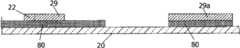
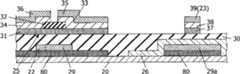
如图2所示,在与对置基板10对置的薄膜晶体管基板20的内面,由CrO2(氧化铬)构成的防反射膜80分别与扫描线22及数据线23对置地形成。该防反射膜80形成为比形成扫描线22及数据线23的区域宽。另外,防反射膜80除了CrO2以外,例如也可以由感光(光敏)黑色聚酰亚胺等的感光树脂形成。As shown in FIG. 2 ,
此外,在薄膜晶体管基板20的内面侧,在其规定的地方形成有由Cr(铬)等构成的栅极电极29、以及与该栅极电极29连接的扫描线22。栅极电极29以及扫描线22形成在防反射膜80上。栅极电极29配置在构成薄膜晶体管29的地方。此外,在薄膜晶体管基板20的内面侧的其他规定的地方,形成有由Cr等构成的栅极布线29a、覆盖栅极布线29a的由ITO(氧化锡铟)等构成的辅助容量线26。栅极布线29a形成在防反射膜80上,辅助容量线26形成为覆盖这些栅极布线29a以及防反射膜80两者。In addition,
并且,在薄膜晶体管基板20形成有例如由氧化硅或氮化硅等构成的栅极绝缘膜30,以覆盖栅极电极29、扫描线22及辅助容量线26。由此,栅极电极29配置在栅极绝缘膜30的下层侧。Furthermore, a
在栅极绝缘膜30的上面的栅极电极29上方,形成有例如由本征非晶形硅等的半导体构成的半导体薄膜31。在该半导体薄膜31的上面的大致中央部设有由氮化硅等构成的沟道保护膜32。在沟道保护膜32的上面两侧及其两侧的半导体薄膜31的上面,设有由n型非晶形硅等构成的欧姆接触层33、34。A semiconductor
在欧姆接触层33、34的上面,设有例如由Cr构成的源极电极35及漏极电极36。由此,在栅极绝缘膜30的上层侧配置源极电极35及漏极电极36。这里,薄膜晶体管25为反交错型,由栅极电极29、栅极绝缘膜30、半导体薄膜31、沟道保护膜32、欧姆接触层33、34、源极电极35以及漏极电极36构成。On the upper surfaces of the ohmic contact layers 33 and 34, a
此外,在栅极绝缘膜30的上面的数据线23的形成区域,也形成有例如由本征非晶形硅等的半导体构成的半导体薄膜37。在半导体薄膜37的上面,设有由n型非晶形硅等构成的欧姆接触层38。并且,在欧姆接触层38的上面形成有由铬等构成的漏极膜39。该漏极膜39构成数据线23。In addition, a semiconductor
并且,在薄膜晶体管25及数据线23的上层侧,形成有由氧化硅等构成的作为层间绝缘膜的外敷膜50,以覆盖这些薄膜晶体管25及数据线23。在该外敷膜50的源极电极35的上面形成有接触孔40。具体而言,接触孔40相对于源极电极35的从沟道保护膜32离开的部分的上面而形成。Furthermore, an
在外敷膜50的上面的规定的地方,如图2及图3所示,由ITO等构成的透明性的像素电极24以经由接触孔40而与源极电极35及辅助容量线26电连接的方式形成。At predetermined places on the upper surface of the
并且,在薄膜晶体管基板20,例如由感光丙烯等的感光树脂形成了从扫描线22及数据线23上朝向对置面板10而立设的隔壁60。隔壁60的截面大致形成为梯形状,其底边部60a形成为比扫描线22及数据线23的宽度宽,以覆盖这些线22、23。Further, on the thin
下面,参照图4~图6说明电泳显示装置1的制造方法。Next, a method of manufacturing the
首先,如图4A所示,对于薄膜晶体管基板20的内面,在规定地方使氧化铬成膜,形成防反射膜80。First, as shown in FIG. 4A , on the inner surface of the thin
并且,如图4B所示,在防反射膜80的规定地方,使Cr成膜,并形成栅极电极29、扫描线22及栅极布线29a。Then, as shown in FIG. 4B , Cr is deposited on a predetermined portion of the
然后,如图4C所示,使ITO成膜以覆盖栅极布线29a,而形成辅助容量线26。Then, as shown in FIG. 4C , an ITO film is formed to cover the
接着,如图4D所示,例如使氧化硅或氮化硅等成膜以覆盖栅极电极29、扫描线22及辅助容量线26,从而形成栅极绝缘膜30。在形成栅极绝缘膜30之后,在其上面使本征非晶形硅31a成膜。进而,在形成本征非晶形硅31a之后,在其上面的规定地方使氮化硅等成膜而形成沟道保护膜32。Next, as shown in FIG. 4D , for example, silicon oxide or silicon nitride is deposited to cover the
此外,如图5A所示,利用周知的蚀刻法等去除本征非晶形硅31a的不需要的部分,形成半导体薄膜31、37。在去除之后,在规定地方使n形非晶形硅等成膜而形成欧姆接触层33、34、38,并在该欧姆接触层33、34、38上使Cr成膜而形成源极电极35、漏极电极36以及漏极膜39。由此,形成薄膜晶体管25及数据线23。Further, as shown in FIG. 5A , unnecessary portions of the intrinsic
如图5B所示,在薄膜晶体管25及数据线23的上层侧,使氧化硅等成膜而形成外敷膜50。然后,通过周知的蚀刻法去除外敷膜50的规定地方,形成接触孔40。As shown in FIG. 5B , on the upper layer side of the
并且,如图5C所示,在外敷膜50的上面的规定的地方,使ITO成膜而形成像素电极24。Then, as shown in FIG. 5C , at predetermined places on the upper surface of the
若完成薄膜晶体管基板20,则在薄膜晶体管基板20上形成隔壁60。具体而言,利用图6所示的隔壁用膜61形成隔壁60。在图6中示出了各层被剥离的状态,但实际上,隔壁用膜61是支承膜62、抗蚀膜63以及盖膜64层叠而形成的。例如,支承膜62由PET等树脂膜形成,盖膜64由OPP等树脂膜形成。并且,抗蚀膜63由构成隔壁60的感光丙烯等感光树脂形成,在一个面上粘贴了支承膜62,在另一个面上粘贴了盖膜64。When the thin
为了利用该隔壁用膜61来形成隔壁60,首先将盖膜64剥掉,而在薄膜晶体管基板20上贴合抗蚀膜63。在该状态下将抗蚀膜63曝光,将感光丙烯复制到薄膜晶体管基板20的规定位置。在复制之后,将支承膜62剥掉,然后将抗蚀膜63进行显影而去除复制到薄膜晶体管基板20上的部分以外的部分。并且,对复制到薄膜晶体管基板20上的感光丙烯施加后烘烤,提高密合性,从而如图2所示形成隔壁60。In order to form the
在形成隔壁60之后,将分散有多个黑粒子71、白粒子72的溶媒70注入至由隔壁60包围的多个区域。注入后,将对置基板10配置在薄膜晶体管基板20上以使对置电极11和像素电极24对置,并通过在对置的基板10、20之间形成的未图示的框状的密封材料进行贴合和密封。或者,也可以在对置基板10的整个面上预先利用树脂膜等来形成粘接层,并贴合和密封(参照图1)。After the
下面,对第一实施方式的电泳显示装置1的作用进行说明。另外,在电泳显示装置1中,显示面为薄膜晶体管基板20的外面20a,进行视觉辨认的方向为图1的箭头方向。Next, the operation of the
并且,若将对置电极11的电压设为比像素电极24高,则带负电的由氧化钛构成的白粒子72向对置电极11侧移动,并且带正电的由炭黑构成的黑粒子71向像素电极24侧移动,从而在显示面上显示黑色(例如,图1所示的状态)。反之,若将对置电极11的电压设为比像素电极24小,则白粒子72向像素电极24侧移动,并且黑粒子71向对置电极11侧移动,从而在显示面上显示白色。对配置在矩阵上的每一个像素进行这些,由此在显示面上描绘规定的图形或文字。And, when the voltage of the
如图1所示,在制造之后,隔壁60与对置基板10之间残存黑粒子71、白粒子72,是被夹持在对置基板10的状态。若将对置基板10侧设为显示面,则由于在像素间存在与想要显示的颜色相反的颜色的粒子(图1中为白粒子72),因此引起对比度的下降,但在该电泳显示装置1中,薄膜晶体管基板20的外面20a为显示面,因此即使在像素间存在与想要显示的颜色相反的颜色的粒子(图1中为白粒子72),也能够防止该粒子显示在显示面上,并且防止对比率的下降。As shown in FIG. 1 , after manufacture,
并且,在以薄膜晶体管基板20的外面20a为显示面的情况下,由于扫描线22及数据线23由金属模形成,因此会产生镜面反射,反光变得强烈。因此,在第一实施方式的电泳显示装置1中,在扫描线22及数据线23与薄膜晶体管基板20之间夹入了防反射膜80,以使其与扫描线线22及数据线23重叠,因此即使从显示面侧进行视觉辨认,也能够防止上述的反光,且防止显示品质的下降。In addition, when the
如上所述,根据第一实施方式,能够提供可抑制反光并且防止对比率的下降的电泳显示装置1。As described above, according to the first embodiment, it is possible to provide the
此外,由于防反射膜80形成为比形成扫描线22及数据线23的区域更宽,因此即使扫描线22及数据线23存在位置偏移,也能够由防反射膜80可靠地覆盖显示面侧。In addition, since the
[第二实施方式][Second Embodiment]
下面,参照附图对本发明的第二实施方式进行说明。这里,在第二实施方式的说明中,对与第一实施方式的不同点进行说明,对于与第一实施方式相同的部分赋予相同的符号,并省略其说明。Next, a second embodiment of the present invention will be described with reference to the drawings. Here, in the description of the second embodiment, differences from the first embodiment will be described, and the same reference numerals will be assigned to the same parts as in the first embodiment, and descriptions thereof will be omitted.
图7是示意地表示第二实施方式的电泳显示装置的要部结构的截面图。如该图7所示,在电泳显示装置1中,设有:对置基板10;以及薄膜晶体管基板20,通过将上面60b形成为凸状的曲面的隔壁60,以规定的间隔与对置基板10对置配置。7 is a cross-sectional view schematically showing the configuration of main parts of an electrophoretic display device according to a second embodiment. As shown in FIG. 7 , in the
图8是图3的II-II截面图,与第一实施方式的图2的不同点是上面60b形成为凸状的曲面的隔壁60。FIG. 8 is a cross-sectional view taken along line II-II of FIG. 3 , and differs from FIG. 2 of the first embodiment in that the
为了使隔壁60的上面60b成为凸的曲面,而在形成隔壁60时,通过实施过曝光或过蚀刻,来去除隔壁60的上部的角,从而上面60b成为凸的曲面。In order to make the
在形成隔壁60后,将分散有多个黑粒子71、白粒子72的溶媒70注入至由隔壁60包围的多个区域。这里,在注入溶媒70时,将要放置在隔壁60上的黑粒子71、白粒子72沿着隔壁60的上面60b的曲面向下方流下。由此,降低在隔壁60的上部残存的粒子量。After the
在注入后,以对置电极11与像素电极24对置的方式将对置基板10配置在薄膜晶体管基板20上,并通过未图示的框状的密封材料粘贴并密封。这里也在注入溶媒70时,放置在隔壁60上的黑粒子71、白粒子72在将隔壁60与对置基板10的内面抵接的过程中沿着曲面60b被排除,只不过是直径比黑粒子71小的白粒子72被夹持在隔壁60的上面60b的曲面的前端部分与对置基板10之间而残留一点。由此,隔壁60与对置基板10抵接(参照图7)。After implantation, the
在如上所述的制造后,在隔壁60的上面60b上几乎没有残存黑粒子71及白粒子72,但如图7所示,虽然是一点点,但在隔壁60的上面60b上残存黑粒子71及白粒子72,成为被对置基板10夹持的状态。在该电泳显示装置1中,由于薄膜晶体管基板20的外面20a成为显示面,因此即使在像素间存在与想要显示的颜色相反的颜色的粒子(在图7中为白粒子72),也能够防止从显示面观察到该粒子,而能够防止对比率的下降。After manufacturing as described above, almost no
另外,一般在将薄膜晶体管基板20的外面20a作为了显示面的情况下,扫描线22及数据线23会引起镜面反射,导致反光强烈。因此,在本实施方式的电泳显示装置1中,在扫描线22及数据线23与薄膜晶体管基板20之间,夹入防反射膜80,以使其与扫描线22及数据线23重叠,因此,即使从显示面侧进行视觉辨认,也能够方式上述的反光。In addition, generally when the
如上所述,根据第二实施方式,能够提供可抑制反光并且防止对比度的下降的电泳显示装置1。As described above, according to the second embodiment, it is possible to provide the
此外,由于防反射膜80形成为比形成扫描线22及数据线23的区域宽,因此,即使在扫描线22及数据线23存在位置偏移,也能够由防反射膜80可靠地覆盖显示面侧。In addition, since the
此外,由于隔壁60的上面60b与对置基板10抵接,因此在隔壁60的上面60b上难以残存粒子71、72,对置基板10与薄膜晶体管基板20的间隔保持一定,因此能够抑制像素之间的对比度不均匀。In addition, since the
另外,本发明不限于上述实施方式,而可进行适当变更。In addition, this invention is not limited to the said embodiment, It can change suitably.
例如,在第二实施方式中,以隔壁60的上面60b与对置基板10抵接的情况为例进行了说明,但隔壁60的上面60b与对置基板10可以隔开规定的间隔。在该情况下,优选的是,将隔壁60的上面60b与对置基板10的间隔设定为比两种粒子71、72中小的粒子(在第二实施方式中为白粒子72)的直径还小。由此,在隔壁60的上面60b上难以残存粒子71、72,能够进一步抑制对比率的下降。为了隔开规定的间隔,只要将比隔壁60的高度大的规定的粒子直径的间隔件(珠子等)混合到密封剂中即可。For example, in the second embodiment, the case where the
另外,在第二实施方式中,以对置基板10及薄膜晶体管基板20由玻璃基板形成的情况为例进行了说明,但这些基板10、20中的至少一方可以由PET基板等挠性基板形成。例如,若考虑对置基板10为挠性基板的情况,则由于对置基板10的挠度而会在隔壁60与对置基板10之间开出流路。这是将电泳显示装置立起来时明显产生的现象。在出现该现象时,如图10所示,在以往的电泳显示装置100中,在隔壁105的上部会大量残存粒子直径比作为流路的间隙大的黑粒子108a,有发生黑显示斑点或条纹的问题。但是,如果是第二实施方式的电泳显示装置1,则如图7所示,由于隔壁60的上面60b为凸的曲面,因此,粒子71、71本身难以在隔壁60的上部的像素间残存。由此,在一对基板10、20的至少一方由挠性基板形成的情况下,也能够抑制黑显示斑点或条纹的产生。In addition, in the second embodiment, the case where the
并且,如果对置基板10及薄膜晶体管基板20两者均由挠性基板形成,则对于显示部分整体为挠性的电泳显示装置,也能够抑制黑显示斑点或黑条纹的产生。Furthermore, if both the
并且,在第二实施方式的电泳显示装置1中,例示了显示面为薄膜晶体管基板20的外面20a的情况,但也可以为如图9所示的电泳显示装置1A那样,将显示面作为对置基板10的外面10a。在这样的情况下,也在隔壁60与对置基板10之间几乎没有残存粒子71、72,因此在像素间难以存在与想要显示的颜色相反的颜色的粒子(在图9中为黑粒子71)。因此,即使将对置基板10的外面10a作为显示面,也能够抑制对比率的下降。进而,在将对置基板10的外面10a作为显示面的情况下,扫描线22及数据线23成为背面侧,因此也不需要考虑这些线22、23的镜面反射。即,能够省略防反射膜80,并能够减少制造成本。In addition, in the
Claims (20)
Translated fromChineseApplications Claiming Priority (4)
| Application Number | Priority Date | Filing Date | Title |
|---|---|---|---|
| JP2009149359AJP4831211B2 (en) | 2009-06-24 | 2009-06-24 | Electrophoretic display device |
| JP2009149357AJP4735744B2 (en) | 2009-06-24 | 2009-06-24 | Electrophoretic display device |
| JP149359/2009 | 2009-06-24 | ||
| JP149357/2009 | 2009-06-24 |
Publications (2)
| Publication Number | Publication Date |
|---|---|
| CN101930147Atrue CN101930147A (en) | 2010-12-29 |
| CN101930147B CN101930147B (en) | 2012-11-28 |
Family
ID=43369405
Family Applications (1)
| Application Number | Title | Priority Date | Filing Date |
|---|---|---|---|
| CN2010102163861AExpired - Fee RelatedCN101930147B (en) | 2009-06-24 | 2010-06-23 | Electrophoretic displaying apparatus |
Country Status (4)
| Country | Link |
|---|---|
| US (1) | US8111449B2 (en) |
| KR (1) | KR20100138762A (en) |
| CN (1) | CN101930147B (en) |
| TW (1) | TWI456327B (en) |
Cited By (5)
| Publication number | Priority date | Publication date | Assignee | Title |
|---|---|---|---|---|
| CN103149766A (en)* | 2013-02-28 | 2013-06-12 | 京东方科技集团股份有限公司 | Electrophoretic display device and preparation method thereof |
| CN103309113A (en)* | 2012-03-16 | 2013-09-18 | 富士施乐株式会社 | Display medium and display device |
| CN108303832A (en)* | 2018-02-13 | 2018-07-20 | 京东方科技集团股份有限公司 | A kind of electronic-paper display screen and its driving method, display device of electronic paper |
| CN112631035A (en)* | 2015-01-05 | 2021-04-09 | 伊英克公司 | Electro-optic display and method for driving an electro-optic display |
| CN114859620A (en)* | 2022-05-18 | 2022-08-05 | 无锡威峰科技股份有限公司 | Display plasma module with supporting and blocking retaining wall structure and plasma display screen |
Families Citing this family (9)
| Publication number | Priority date | Publication date | Assignee | Title |
|---|---|---|---|---|
| JP2012027163A (en)* | 2010-07-22 | 2012-02-09 | Casio Comput Co Ltd | Electrophoretic display device |
| KR101409430B1 (en)* | 2010-12-16 | 2014-06-20 | 코오롱인더스트리 주식회사 | Preparation method of electrophoresis display device |
| KR101759643B1 (en)* | 2010-12-17 | 2017-08-01 | 삼성디스플레이 주식회사 | Electrophoresis display apparatus |
| US20120275013A1 (en)* | 2011-04-19 | 2012-11-01 | Seiko Epson Corporation | Display sheet, method of manufacturing display sheet, display device and electronic apparatus |
| TWI479249B (en)* | 2012-04-25 | 2015-04-01 | Hsiung Kuang Tsai | Reflective visual interface apparatus |
| KR101486363B1 (en)* | 2012-08-22 | 2015-01-26 | 엘지디스플레이 주식회사 | Organic Light Emitting Diode Display Device |
| US10705404B2 (en)* | 2013-07-08 | 2020-07-07 | Concord (Hk) International Education Limited | TIR-modulated wide viewing angle display |
| KR102086805B1 (en)* | 2013-11-19 | 2020-03-09 | 엘지디스플레이 주식회사 | Organic Light Emitting Display Device |
| JP2016148795A (en)* | 2015-02-13 | 2016-08-18 | セイコーエプソン株式会社 | Electrophoretic display device, electrophoretic display device manufacturing method, and electronic apparatus |
Citations (5)
| Publication number | Priority date | Publication date | Assignee | Title |
|---|---|---|---|---|
| US20040160187A1 (en)* | 2003-02-18 | 2004-08-19 | Fuji Xerox Co., Ltd. | Image display medium ribs, production process thereof, and image display medium using the ribs |
| JP2005221520A (en)* | 2004-02-03 | 2005-08-18 | Toshiba Corp | Electrophoretic display device |
| JP2007034037A (en)* | 2005-07-28 | 2007-02-08 | Canon Inc | Particle movement type display device |
| CN101093335A (en)* | 2006-06-22 | 2007-12-26 | 三星电子株式会社 | Electrophoretic display and manufacturing method thereof |
| CN101393370A (en)* | 2007-09-21 | 2009-03-25 | 株式会社半导体能源研究所 | Electrophoretic display device and manufacturing method thereof |
Family Cites Families (9)
| Publication number | Priority date | Publication date | Assignee | Title |
|---|---|---|---|---|
| US7999787B2 (en)* | 1995-07-20 | 2011-08-16 | E Ink Corporation | Methods for driving electrophoretic displays using dielectrophoretic forces |
| JP4940157B2 (en) | 2003-09-25 | 2012-05-30 | 株式会社 日立ディスプレイズ | Driving method of display device |
| JP4160521B2 (en) | 2004-03-08 | 2008-10-01 | 株式会社東芝 | Electrophoretic display device |
| JP2006058544A (en) | 2004-08-19 | 2006-03-02 | Bridgestone Corp | Panel for picture display and method for manufacturing the same |
| KR20070009015A (en) | 2005-07-14 | 2007-01-18 | 삼성전자주식회사 | Driving Method of Electrophoretic Display and Electrophoretic Display |
| EP1785767A1 (en)* | 2005-11-09 | 2007-05-16 | Bridgestone Corporation | Information display panel |
| JP2008139519A (en) | 2006-11-30 | 2008-06-19 | Brother Ind Ltd | Display medium and display device |
| US7936498B2 (en)* | 2007-03-08 | 2011-05-03 | Ricoh Company, Ltd. | Display element, image display device, and image display system |
| JP2009223094A (en) | 2008-03-18 | 2009-10-01 | Brother Ind Ltd | Display device and display rewriting method in display device |
- 2010
- 2010-06-14KRKR1020100056020Apatent/KR20100138762A/ennot_activeCeased
- 2010-06-22TWTW099120180Apatent/TWI456327B/ennot_activeIP Right Cessation
- 2010-06-22USUS12/820,287patent/US8111449B2/enactiveActive
- 2010-06-23CNCN2010102163861Apatent/CN101930147B/ennot_activeExpired - Fee Related
Patent Citations (5)
| Publication number | Priority date | Publication date | Assignee | Title |
|---|---|---|---|---|
| US20040160187A1 (en)* | 2003-02-18 | 2004-08-19 | Fuji Xerox Co., Ltd. | Image display medium ribs, production process thereof, and image display medium using the ribs |
| JP2005221520A (en)* | 2004-02-03 | 2005-08-18 | Toshiba Corp | Electrophoretic display device |
| JP2007034037A (en)* | 2005-07-28 | 2007-02-08 | Canon Inc | Particle movement type display device |
| CN101093335A (en)* | 2006-06-22 | 2007-12-26 | 三星电子株式会社 | Electrophoretic display and manufacturing method thereof |
| CN101393370A (en)* | 2007-09-21 | 2009-03-25 | 株式会社半导体能源研究所 | Electrophoretic display device and manufacturing method thereof |
Cited By (9)
| Publication number | Priority date | Publication date | Assignee | Title |
|---|---|---|---|---|
| CN103309113A (en)* | 2012-03-16 | 2013-09-18 | 富士施乐株式会社 | Display medium and display device |
| CN103149766A (en)* | 2013-02-28 | 2013-06-12 | 京东方科技集团股份有限公司 | Electrophoretic display device and preparation method thereof |
| WO2014131243A1 (en)* | 2013-02-28 | 2014-09-04 | 京东方科技集团股份有限公司 | Electrophoretic display device and manufacturing method thereof |
| CN103149766B (en)* | 2013-02-28 | 2016-05-11 | 京东方科技集团股份有限公司 | The preparation method of a kind of electrophoretic display apparatus and electrophoretic display apparatus |
| US9470949B2 (en) | 2013-02-28 | 2016-10-18 | Chengdu Boe Optoelectronics Technology Co., Ltd. | Electrophoretic display device and method for manufacturing the same |
| CN112631035A (en)* | 2015-01-05 | 2021-04-09 | 伊英克公司 | Electro-optic display and method for driving an electro-optic display |
| CN108303832A (en)* | 2018-02-13 | 2018-07-20 | 京东方科技集团股份有限公司 | A kind of electronic-paper display screen and its driving method, display device of electronic paper |
| CN114859620A (en)* | 2022-05-18 | 2022-08-05 | 无锡威峰科技股份有限公司 | Display plasma module with supporting and blocking retaining wall structure and plasma display screen |
| CN114859620B (en)* | 2022-05-18 | 2023-11-10 | 无锡威峰科技股份有限公司 | Display plasma module with supporting barrier wall structure and plasma display screen |
Also Published As
| Publication number | Publication date |
|---|---|
| TW201106080A (en) | 2011-02-16 |
| TWI456327B (en) | 2014-10-11 |
| CN101930147B (en) | 2012-11-28 |
| US20100328756A1 (en) | 2010-12-30 |
| KR20100138762A (en) | 2010-12-31 |
| US8111449B2 (en) | 2012-02-07 |
Similar Documents
| Publication | Publication Date | Title |
|---|---|---|
| CN101930147B (en) | Electrophoretic displaying apparatus | |
| US8427737B2 (en) | Electrophoretic display device | |
| US8421973B2 (en) | Liquid crystal display device | |
| CN103543561B (en) | Liquid crystal display device | |
| US10042213B2 (en) | Display device including projections opposed to each other in a sealant | |
| KR20080039147A (en) | Electrophoretic display device and manufacturing method thereof | |
| US20130286312A1 (en) | Display device and manufacturing method thereof | |
| JP2004272012A (en) | Display apparatus | |
| US11294216B2 (en) | Display substrate and display device | |
| JP2017116797A (en) | Liquid crystal display | |
| KR100760940B1 (en) | LCD and its manufacturing method | |
| JP5066943B2 (en) | Liquid crystal display | |
| KR20140086395A (en) | Liquid crystal display device and Method for manufacturing the same | |
| JP5143664B2 (en) | LCD panel | |
| CN111952321B (en) | Display device and array structure | |
| US9810936B2 (en) | Display panel | |
| JP6676793B2 (en) | Display device | |
| CN101427176A (en) | Liquid crystal display device, and its manufacturing method | |
| JP5605051B2 (en) | Electrophoretic display device | |
| JP4831211B2 (en) | Electrophoretic display device | |
| JP4735744B2 (en) | Electrophoretic display device | |
| CN223450293U (en) | Liquid crystal display device having a light shielding layer | |
| JP6739564B2 (en) | Liquid crystal display | |
| JP2017116949A (en) | Display panel | |
| CN118276368A (en) | Electronic paper display device and manufacturing method thereof |
Legal Events
| Date | Code | Title | Description |
|---|---|---|---|
| C06 | Publication | ||
| PB01 | Publication | ||
| C10 | Entry into substantive examination | ||
| SE01 | Entry into force of request for substantive examination | ||
| C14 | Grant of patent or utility model | ||
| GR01 | Patent grant | ||
| CF01 | Termination of patent right due to non-payment of annual fee | Granted publication date:20121128 Termination date:20160623 | |
| CF01 | Termination of patent right due to non-payment of annual fee |