CN101926008B - Field Effect Transistor Using Amorphous Oxide - Google Patents
Field Effect Transistor Using Amorphous OxideDownload PDFInfo
- Publication number
- CN101926008B CN101926008BCN2009801030020ACN200980103002ACN101926008BCN 101926008 BCN101926008 BCN 101926008BCN 2009801030020 ACN2009801030020 ACN 2009801030020ACN 200980103002 ACN200980103002 ACN 200980103002ACN 101926008 BCN101926008 BCN 101926008B
- Authority
- CN
- China
- Prior art keywords
- field effect
- equal
- effect transistor
- film
- transistor
- Prior art date
- Legal status (The legal status is an assumption and is not a legal conclusion. Google has not performed a legal analysis and makes no representation as to the accuracy of the status listed.)
- Expired - Fee Related
Links
Images


Classifications
- H—ELECTRICITY
- H10—SEMICONDUCTOR DEVICES; ELECTRIC SOLID-STATE DEVICES NOT OTHERWISE PROVIDED FOR
- H10D—INORGANIC ELECTRIC SEMICONDUCTOR DEVICES
- H10D30/00—Field-effect transistors [FET]
- H10D30/60—Insulated-gate field-effect transistors [IGFET]
- H10D30/67—Thin-film transistors [TFT]
- H10D30/674—Thin-film transistors [TFT] characterised by the active materials
- H10D30/6755—Oxide semiconductors, e.g. zinc oxide, copper aluminium oxide or cadmium stannate
- H—ELECTRICITY
- H01—ELECTRIC ELEMENTS
- H01L—SEMICONDUCTOR DEVICES NOT COVERED BY CLASS H10
- H01L21/00—Processes or apparatus adapted for the manufacture or treatment of semiconductor or solid state devices or of parts thereof
- H01L21/02—Manufacture or treatment of semiconductor devices or of parts thereof
- H01L21/02104—Forming layers
- H01L21/02365—Forming inorganic semiconducting materials on a substrate
- H01L21/02518—Deposited layers
- H01L21/02521—Materials
- H01L21/02565—Oxide semiconducting materials not being Group 12/16 materials, e.g. ternary compounds
Landscapes
- Engineering & Computer Science (AREA)
- Physics & Mathematics (AREA)
- Condensed Matter Physics & Semiconductors (AREA)
- General Physics & Mathematics (AREA)
- Manufacturing & Machinery (AREA)
- Computer Hardware Design (AREA)
- Microelectronics & Electronic Packaging (AREA)
- Power Engineering (AREA)
- Thin Film Transistor (AREA)
- Liquid Crystal (AREA)
- Electroluminescent Light Sources (AREA)
- Dram (AREA)
Abstract
Description
Translated fromChinese技术领域technical field
本发明涉及一种使用非晶氧化物的场效应晶体管。The present invention relates to a field effect transistor using amorphous oxide.
背景技术Background technique
场效应晶体管(FET)包括栅极电极、源极电极和漏极电极,并且是电子有源器件,其通过借助于对栅极电极的电压施加来控制进入沟道层的电流的流动来控制源极电极与漏极电极之间的电流。将绝缘基板(例如陶瓷、玻璃或塑料基板)上淀积的薄膜用作沟道层的FET具体地被称为薄膜晶体管(TFT)。A field effect transistor (FET) includes a gate electrode, a source electrode, and a drain electrode, and is an electronically active device that controls the source by controlling the flow of current into the channel layer by means of voltage application to the gate electrode. The current flow between the pole electrode and the drain electrode. A FET using a thin film deposited on an insulating substrate such as a ceramic, glass or plastic substrate as a channel layer is specifically called a thin film transistor (TFT).
上述TFT是通过使用薄膜技术而被形成的,故此TFT具有易于形成在具有相对大面积的基板上的优点,因此广泛用作平板显示器(例如液晶显示器)的驱动器件。具体地说,有源液晶显示器(ALCD)通过使用玻璃基板上形成的TFT来开启/关断每一图像像素。此外,对于未来高性能有机LED显示器(OLED),由TFT控制每一像素的电流是有效的。此外,具有更高性能的液晶显示器被实现,其中,具有驱动并且控制整个图像的功能的外围电路通过使用TFT而在图像区域附近被形成在基板上。The above-mentioned TFT is formed by using a thin film technology, so the TFT has an advantage of being easily formed on a substrate having a relatively large area, and thus is widely used as a driving device of a flat panel display such as a liquid crystal display. Specifically, an active liquid crystal display (ALCD) turns on/off each image pixel by using TFTs formed on a glass substrate. In addition, for future high-performance organic LED displays (OLEDs), it is effective to control the current of each pixel by TFT. In addition, a liquid crystal display having higher performance is realized in which a peripheral circuit having a function of driving and controlling an entire image is formed on a substrate near an image area by using TFTs.
目前最流行的TFT是采用多晶硅膜或非晶硅膜作为沟道层材料的TFT。用于像素驱动的非晶硅TFT以及用于全局图像驱动/控制的高性能多晶硅TFT已经投入实际使用。The most popular TFT at present is a TFT using a polysilicon film or an amorphous silicon film as a channel layer material. Amorphous silicon TFTs for pixel driving and high-performance polysilicon TFTs for global image driving/control have been put into practical use.
过去开发出来的TFT(包括非晶硅TFT和多晶硅TFT)的缺点在于,在制造这些器件中需要高温工艺,这使得难以将TFT形成在塑料板、膜、或其它相似的基板上。A disadvantage of TFTs developed in the past, including amorphous silicon TFTs and polysilicon TFTs, is that high temperature processes are required in manufacturing these devices, which makes it difficult to form TFTs on plastic plates, films, or other similar substrates.
同时,开发柔性显示器近年来已经变得活跃,在柔性显示器中,形成在树脂基板(例如聚合体板或膜)上的TFT充当LCD或OLED的驱动电路。这将注意力吸引到有机半导体膜,作为可以淀积在塑料等上的材料,有机半导体膜可以在低温被淀积,并且具有电导率。Meanwhile, development of flexible displays in which TFTs formed on a resin substrate such as a polymer plate or film serve as a driving circuit for LCDs or OLEDs has become active in recent years. This draws attention to organic semiconductor films, which can be deposited at low temperatures and have electrical conductivity, as materials that can be deposited on plastics and the like.
并五苯是有机半导体膜的示例,并且其研究和开发正在进行。据报道,并五苯的载流子迁移率大约是0.5cm2/Vs,其等于非晶Si TFT的载流子迁移率。Pentacene is an example of an organic semiconductor film, and research and development thereof are ongoing. The carrier mobility of pentacene is reported to be about 0.5 cm2 /Vs, which is equal to that of amorphous Si TFT.
然而,并五苯和其它有机半导体具有的问题是:热稳定性低(<150℃),并且尚未成功地制造出在实际使用中可用的器件。However, pentacene and other organic semiconductors have problems in that thermal stability is low (<150° C.), and devices usable in practical use have not been successfully fabricated.
作为可应用于TFT的沟道层的近来已经引起关注的另一材料是氧化物材料。例如,使用具有ZnO作为主要组分的透明导电氧化物多晶薄膜作为沟道层的TFT正在被积极开发。这种薄膜可以在相对低的温度淀积并且形成在塑料板、膜或其它相似的树脂基板上。然而,通常,具有ZnO作为主要组分的化合物无法在室温形成稳定非晶态,而是形成多晶态,这在多晶晶界中产生电子散射,并且使得难以增加电子迁移率。此外,这种多晶化合物的电特性极大地受可能取决于膜淀积条件等的制造工艺的多晶颗粒的形状和互连所影响,因此所得到的TFT器件在某些情况下具有波动特性。Another material that has recently attracted attention as a channel layer applicable to TFTs is an oxide material. For example, a TFT using a transparent conductive oxide polycrystalline thin film having ZnO as a main component as a channel layer is being actively developed. Such thin films can be deposited at relatively low temperatures and formed on plastic plates, films, or other similar resin substrates. However, in general, compounds having ZnO as a main component fail to form a stable amorphous state at room temperature but form a polycrystalline state, which causes electron scattering in polycrystalline grain boundaries and makes it difficult to increase electron mobility. In addition, the electrical characteristics of such polycrystalline compounds are greatly affected by the shape and interconnection of polycrystalline grains that may depend on the manufacturing process such as film deposition conditions, so the resulting TFT devices have fluctuating characteristics in some cases .
关于这个问题,使用基于In-Ga-Zn-O的非晶氧化物的薄膜晶体管已经报道于K.Nomura et al.,Nature vol.432,pp.488-492(2004-11)中。该晶体管可以在室温形成在塑料或玻璃基板上。晶体管还实现具有大约6至9的场效应迁移率的常断型晶体管的特性。另一有利特性在于,晶体管关于可见光是透明的。具体地说,上述文献描述了一种使用具有In∶Ga∶Zn=1.1∶1.1∶0.9的组成比率(原子比率)的非晶氧化物用于TFT的沟道层的技术。Regarding this issue, a thin film transistor using an In-Ga-Zn-O-based amorphous oxide has been reported in K. Nomura et al., Nature vol. 432, pp. 488-492 (2004-11). The transistor can be formed on a plastic or glass substrate at room temperature. The transistor also realizes the characteristics of a normally-off transistor having a field effect mobility of about 6 to 9. Another advantageous property is that the transistor is transparent with respect to visible light. Specifically, the above document describes a technique of using an amorphous oxide having a composition ratio (atomic ratio) of In:Ga:Zn=1.1:1.1:0.9 for a channel layer of a TFT.
虽然使用三种金属元素In、Ga和Zn的非晶氧化物在上述文献中被采用,但就组分控制和材料调整的容易性而言,更好的是,使用更少数量的金属元素。Although amorphous oxides using three metal elements In, Ga, and Zn are employed in the above documents, it is better to use a smaller amount of metal elements in terms of composition control and ease of material adjustment.
另一方面,当通过溅射或相似方法淀积时,使用一种类型的金属元素的氧化物(例如ZnO和In2O3)通常形成多晶薄膜,并且相应地可能如上所述地在TFT器件的特性方面产生波动。On the other hand, when deposited by sputtering or the like, oxides (such as ZnO and In2 O3 ) of one type of metal element are generally used to form a polycrystalline thin film, and accordingly it is possible to form a polycrystalline film as described above in a TFT The characteristics of the device fluctuate.
关于作为使用两种类型的金属元素的示例的基于In-Zn-O的非晶氧化物的研究结果已经从Applied Physics Letters 89,062103(2006)的报告中获知。然而,已知的是,当基于In-Zn-O的非晶氧化物存储于大气中时,该氧化物的电阻率可能改变,由此改善环境是期望的。Research results on In-Zn-O-based amorphous oxides as examples using two types of metal elements have been known from a report in Applied Physics Letters 89, 062103 (2006). However, it is known that when an In-Zn-O-based amorphous oxide is stored in the atmosphere, the resistivity of the oxide may change, and thus improvement of the environment is desired.
此外,关于基于In-Zn-O的非晶氧化物的研究结果已经报道于Solid-State Electronics,50(2006),pp.500-503。在该报告中,执行500℃的热处理,因此期望以较低温度制造器件。这是因为,如果可以在低温制造器件,则可以使用廉价的玻璃基板或树脂基板。In addition, research results on In-Zn-O-based amorphous oxides have been reported in Solid-State Electronics, 50 (2006), pp.500-503. In this report, heat treatment at 500°C was performed, so it is expected to manufacture devices at lower temperatures. This is because an inexpensive glass substrate or resin substrate can be used if the device can be manufactured at low temperature.
因此,由较少数量的金属元素组成的并且具有优异稳定性的非晶氧化物在薄膜晶体管领域是期望的。Therefore, an amorphous oxide composed of a small amount of metal elements and having excellent stability is desired in the field of thin film transistors.
发明内容Contents of the invention
鉴于上述问题而做出本发明,并且因此本发明的一个目的在于提供一种场效应晶体管,其使用由少数量的元素构成的并且展现出较大的通/断比率的非晶氧化物。此外,本发明的另一目的在于提供一种场效应晶体管,其对于大气中的存储具有优异的环境稳定性。The present invention has been made in view of the above problems, and thus an object of the present invention is to provide a field effect transistor using an amorphous oxide composed of a small amount of elements and exhibiting a large on/off ratio. Furthermore, another object of the present invention is to provide a field effect transistor having excellent environmental stability for storage in the atmosphere.
根据本发明的场效应晶体管至少包括形成在基板上的沟道层、栅绝缘层、源极电极、漏极电极和栅极电极,其中,所述沟道层以至少包含In(铟)和B(硼)的非晶氧化物材料制成,并且其中,所述非晶氧化物材料具有等于或大于0.05并且等于或小于0.29的元素比率B/(In+B)。The field effect transistor according to the present invention includes at least a channel layer formed on a substrate, a gate insulating layer, a source electrode, a drain electrode and a gate electrode, wherein the channel layer contains at least In (indium) and B (boron), and wherein the amorphous oxide material has an element ratio B/(In+B) equal to or greater than 0.05 and equal to or less than 0.29.
此外,根据本发明的场效应晶体管至少包括形成在基板上的沟道层、栅绝缘层、源极电极、漏极电极和栅极电极,其中,所述沟道层以至少包含In、Zn和B的非晶氧化物材料制成,并且其中,所述非晶氧化物材料的元素比率B/(In+Zn+B)是等于或大于0.05并且等于或小于0.29。Furthermore, the field effect transistor according to the present invention includes at least a channel layer formed on a substrate, a gate insulating layer, a source electrode, a drain electrode, and a gate electrode, wherein the channel layer contains at least In, Zn and B is made of an amorphous oxide material, and wherein the element ratio B/(In+Zn+B) of the amorphous oxide material is equal to or greater than 0.05 and equal to or less than 0.29.
此外,根据本发明的显示器包括:所述场效应晶体管;以及至少一个像素器件,其具有与所述场效应晶体管的源极电极和漏极电极之一连接的电极。Furthermore, a display according to the present invention includes: the field effect transistor; and at least one pixel device having an electrode connected to one of a source electrode and a drain electrode of the field effect transistor.
根据本发明,所述沟道层以例如包含铟和硼的非晶氧化物的新型材料制成,因此可以实现展现出良好特性的薄膜晶体管。具体地说,本发明实现了这样的效果,即:包括通/断比率和S值的晶体管特性优异,并且环境稳定性良好。According to the present invention, the channel layer is made of a novel material such as amorphous oxide containing indium and boron, so a thin film transistor exhibiting good characteristics can be realized. Specifically, the present invention achieves the effect that transistor characteristics including on/off ratio and S value are excellent, and environmental stability is good.
附图说明Description of drawings
图1是示出基于In-B-O的场效应晶体管的传输特性的曲线图。FIG. 1 is a graph showing transfer characteristics of an In-B-O-based field effect transistor.
图2是示出基于In-B-O的场效应晶体管的电阻率的时间改变的曲线图。FIG. 2 is a graph showing temporal changes in resistivity of an In-B-O-based field effect transistor.
图3A和图3B是示出在基于In-B-O的场效应晶体管、基于In-Al-O的场效应晶体管以及基于In-Ga-O的场效应晶体管之间的特性比较的曲线图,其中,图3A示出待比较的通/断比率,图3B示出待比较的S值。3A and 3B are graphs showing a comparison of characteristics between an In-B-O-based field effect transistor, an In-Al-O-based field effect transistor, and an In-Ga-O-based field effect transistor, wherein, FIG. 3A shows on/off ratios to be compared, and FIG. 3B shows S values to be compared.
图4是示出具有各种元素比率B/(In+B)的基于In-B-O的场效应晶体管的传输特性的曲线图。FIG. 4 is a graph showing transfer characteristics of In-B-O-based field effect transistors having various element ratios B/(In+B).
图5是示出场效应迁移率的元素比率B/(In+B)依赖性的曲线图。FIG. 5 is a graph showing the element ratio B/(In+B) dependence of field-effect mobility.
图6是示出阈值电压的元素比率B/(In+B)依赖性的曲线图。FIG. 6 is a graph showing the element ratio B/(In+B) dependence of the threshold voltage.
图7是示出S值的元素比率B/(In+B)依赖性的曲线图。FIG. 7 is a graph showing the element ratio B/(In+B) dependence of the S value.
图8A、图8B和图8C是示出根据本发明实施例的场效应晶体管的结构示例的截面图。8A , 8B and 8C are cross-sectional views showing structural examples of field effect transistors according to embodiments of the present invention.
图9A和图9B是示出根据本发明实施例的场效应晶体管的特性的示例的曲线图。9A and 9B are graphs showing examples of characteristics of a field effect transistor according to an embodiment of the present invention.
图10是示出用于制造场效应晶体管的薄膜形成装置的结构的示图。FIG. 10 is a diagram showing the structure of a thin film forming apparatus for manufacturing a field effect transistor.
图11是示出基于In-B-O的半导体薄膜的电阻率的元素比率B/(In+B)依赖性的曲线图。11 is a graph showing the dependence of the resistivity of an In-B-O-based semiconductor thin film on the element ratio B/(In+B).
图12是示出根据本发明的显示器的示例的示意性截面图。FIG. 12 is a schematic cross-sectional view showing an example of a display according to the present invention.
图13是示出根据本发明的显示器的另一示例的示意性截面图。Fig. 13 is a schematic cross-sectional view showing another example of a display according to the present invention.
图14是示出其中以二维方式布置均包括有机EL器件和薄膜晶体管的像素的显示器的示意性结构图。FIG. 14 is a schematic structural view showing a display in which pixels each including an organic EL device and a thin film transistor are arranged two-dimensionally.
图15是示出基于In-B-O的半导体薄膜的电阻率的时间改变的曲线图。FIG. 15 is a graph showing temporal changes in resistivity of an In-B-O-based semiconductor thin film.
具体实施方式Detailed ways
描述用于实施本发明的示例性实施例模式。Exemplary embodiment modes for carrying out the present invention are described.
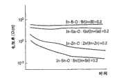
本发明的发明人已经认真研究了包含两种类型的金属元素的氧化物材料(例如包含铟(In)和硼(B)的氧化物)作为薄膜晶体管的沟道层的材料。图2示出通过溅射形成的各种氧化物薄膜的电阻率的时间改变。在图2中,所使用的每一薄膜具有近似0.2的在In与另一金属元素M之间的元素比率M/(In+M)。如从图2明显看出的那样,包含In和Zn的氧化物(In-Zn-O)以及包含In和Sn的氧化物(In-Sn-O)中的每一个的电阻率的时间改变是大的。与之对照,显然,包含In和B的氧化物(In-B-O)以及包含In和Ga的氧化物(In-Ga-O)中的每一个的电阻率的时间改变几乎不出现。氧化物(In-B-O)在电特性方面具有优异的环境稳定性,因此成为期望的半导体材料。The inventors of the present invention have earnestly studied an oxide material including two types of metal elements, such as an oxide including indium (In) and boron (B), as a material of a channel layer of a thin film transistor. FIG. 2 shows temporal changes in resistivity of various oxide thin films formed by sputtering. In FIG. 2, each thin film used has an element ratio M/(In+M) between In and another metal element M of approximately 0.2. As is apparent from FIG. 2, the temporal change in resistivity of each of the oxide containing In and Zn (In-Zn-O) and the oxide containing In and Sn (In-Sn-O) is big. In contrast, it is apparent that the temporal change in resistivity of each of the oxide containing In and B (In-B-O) and the oxide containing In and Ga (In-Ga-O) hardly occurs. Oxide (In-B-O) has excellent environmental stability in terms of electrical characteristics, and thus becomes a desired semiconductor material.
接下来,上述各材料用于沟道,以制造薄膜晶体管的原型。在氧化物(In-Zn-O)和氧化物(In-Sn-O)的每一个的情况下,难以实现具有等于或大于五个数量级的通/断比率的晶体管。与之对照,在氧化物(In-B-O)的情况下,如从图1所示的传输特性(Id-Vg曲线图)显而易见的那样,可以实现具有等于或大于十个数量级的通/断比率的晶体管。Next, the above-mentioned materials are used in the channel to manufacture the prototype of the thin film transistor. In the case of each of oxide (In—Zn—O) and oxide (In—Sn—O), it is difficult to realize a transistor having an on/off ratio equal to or greater than five orders of magnitude. In contrast, in the case of an oxide (In-B-O), as is apparent from the transfer characteristics (Id-Vg graph) shown in FIG. of transistors.
图3A和图3B是其中在氧化物In-M-O(金属元素M是周期表中的III族元素)用于沟道时的晶体管特性彼此比较的曲线图。如图3A所示,包括包含In-B-O的沟道的薄膜晶体管(TFT)展现出比包括包含In-Ga-O的沟道的TFT以及包括包含In-Al-O的沟道的TFT更大的通/断比率。如图3B所示,包括包含In-B-O的沟道的TFT展现出比包括包含In-Ga-O的沟道的TFT以及包括包含In-Al-O的沟道的TFT更小的S值。因此,使用In-B-O用于沟道的TFT展现出期望的晶体管特性。3A and 3B are graphs in which transistor characteristics when an oxide In-M-O (a metal element M is a Group III element in the periodic table) is used for a channel are compared with each other. As shown in FIG. 3A, a thin film transistor (TFT) including a channel including In-B-O exhibits a larger TFT than a TFT including a channel including In-Ga-O and a TFT including a channel including In-Al-O. on/off ratio. As shown in FIG. 3B , the TFT including the channel including In-B-O exhibited a smaller S value than the TFT including the channel including In-Ga-O and the TFT including the channel including In-Al-O. Therefore, a TFT using In-B-O for a channel exhibits desired transistor characteristics.
接下来,详细描述根据本发明的场效应晶体管的实施例。Next, embodiments of the field effect transistor according to the present invention are described in detail.
首先,描述根据该实施例的场效应晶体管的结构。First, the structure of the field effect transistor according to this embodiment is described.
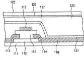
图8A、图8B和图8C是示出根据该实施例的场效应晶体管的结构示例的截面图。在图8A、图8B和图8C中,基板、沟道层、栅绝缘层、源极电极、漏极电极和栅极电极分别由标号10、11、12、13、14和15表示。8A , 8B and 8C are cross-sectional views showing structural examples of the field effect transistor according to this embodiment. In FIGS. 8A, 8B, and 8C, the substrate, channel layer, gate insulating layer, source electrode, drain electrode, and gate electrode are denoted by
根据该实施例的场效应晶体管是三端子器件,包括栅极电极15、源极电极13和漏极电极14。场效应晶体管具有的功能是:将电压Vg施加到栅极电极,控制流过沟道层的电流Id,并且在源极电极与漏极电极之间切换电流Id。The field effect transistor according to this embodiment is a three-terminal device including a
图8A示出其中栅绝缘层12和栅极电极15依次形成在半导体沟道层11上的顶栅结构的示例。此外,图8B示出其中栅绝缘层12和半导体沟道层11依次形成在栅极电极15上的底栅结构的示例。此外,图8C示出底栅晶体管的另一示例。在图8C中,基板(n+Si基板,其还作为栅极电极)、绝缘层(SiO2)、沟道层(氧化物)、源极电极和漏极电极分别由标号21、22、25、23和24表示。FIG. 8A shows an example of a top gate structure in which a
场效应晶体管的结构不限于本发明中的上述结构,并且可以使用任意顶栅/底栅结构或交错/反转交错结构。The structure of the field effect transistor is not limited to the above-mentioned structure in the present invention, and any top-gate/bottom-gate structure or staggered/inverted staggered structure may be used.
接下来更详细地描述构成该实施例的场效应晶体管的组件。Next, components constituting the field effect transistor of this embodiment are described in more detail.
(沟道层)(channel layer)
如上所述,该实施例的场效应晶体管的特征在于,对于沟道层使用至少包含铟和硼的非晶氧化物。包含In和B的非晶氧化物(In-B-O)以及包含In、B和Zn的氧化物(In-Zn-B-O)是特别期望的材料。同样可采用包含In、Sn和B的非晶氧化物。As described above, the field effect transistor of this embodiment is characterized in that an amorphous oxide containing at least indium and boron is used for the channel layer. Amorphous oxides containing In and B (In-B-O) and oxides containing In, B, and Zn (In-Zn-B-O) are particularly desirable materials. Amorphous oxides containing In, Sn, and B can also be used.
在该实施例中,硼对于非晶氧化物中包含的所有金属元素的比率等于或大于10原子%并且等于或小于40原子%。在所有元素当中,以In-B-O制成的非晶氧化物包含的氧的量最大、铟的量第二大以及硼的量第三大。在所有元素当中,以In-Zn-B-O制成的非晶氧化物包含的氧的量最大、锌(或铟)的量第二大、铟(或锌)的量第三大、以及硼的量第四大。In this embodiment, the ratio of boron to all metal elements contained in the amorphous oxide is equal to or greater than 10 atomic % and equal to or less than 40 atomic %. Among all the elements, the amorphous oxide made of In-B-O contains the largest amount of oxygen, the second largest amount of indium, and the third largest amount of boron. Among all elements, the amorphous oxide made of In-Zn-B-O contains the largest amount of oxygen, the second largest amount of zinc (or indium), the third largest amount of indium (or zinc), and the amount of boron The fourth largest volume.
本发明的发明人在对于使用包含铟和硼的非晶氧化物用于沟道层的薄膜晶体管的认真研究期间发现以下事实。也就是说,当具有特定元素比率B/(In+B)的氧化物半导体应用于沟道时,可以实现展现出期望特性的晶体管。The inventors of the present invention discovered the following fact during earnest studies on a thin film transistor using an amorphous oxide containing indium and boron for a channel layer. That is, when an oxide semiconductor having a specific element ratio B/(In+B) is applied to a channel, a transistor exhibiting desired characteristics can be realized.
在对于薄膜晶体管的沟道采用In-B-O是,存在优选的In和B元素比率。优选元素比率B/(In+B)是等于或大于0.05(5原子%),因为,按该元素比率,可以通过在以室温保持基板温度的情况下通过溅射-淀积来获得非晶薄膜。这是因为,如上所述,其中多晶颗粒的形状和互连取决于膜淀积方法而极大变化的多晶态在TFT器件的特性方面引起波动。When In-B-O is used for the channel of the thin film transistor, there is a preferable ratio of In and B elements. It is preferable that the element ratio B/(In+B) is equal to or more than 0.05 (5 atomic %) because, with this element ratio, an amorphous thin film can be obtained by sputtering-deposition while maintaining the substrate temperature at room temperature . This is because, as described above, the polycrystalline state in which the shape and interconnection of polycrystalline grains greatly varies depending on the film deposition method causes fluctuations in the characteristics of the TFT device.
图5是示出当制造使用In-B-O薄膜的场效应晶体管时场效应迁移率对元素比率B/(In+B)的依赖性的示例的曲线图。如从图5显而易见的那样,场效应迁移率随着B的含量减少而变大。所需的场效应迁移率的值取决于场效应晶体管的使用。例如,电泳显示器可以由具有近似0.05cm2/Vs的场效应迁移率的TFT所驱动。液晶显示器可以由具有近似0.1cm2/Vs的场效应迁移率的TFT所驱动。在有机EL显示器中,期望的场效应迁移率等于或大于1cm2/Vs。据此,In与B之间的元素比率B/(In+B)期望地等于或小于0.29,更期望地等于或小于0.22,以及最期望地等于或小于0.2。FIG. 5 is a graph showing an example of the dependence of field effect mobility on the element ratio B/(In+B) when manufacturing a field effect transistor using an In—BO thin film. As is apparent from FIG. 5 , the field effect mobility becomes larger as the B content decreases. The value of field effect mobility required depends on the use of field effect transistors. For example, electrophoretic displays can be driven by TFTs with field effect mobility of approximately 0.05 cm2 /Vs. Liquid crystal displays can be driven by TFTs having a field effect mobility of approximately 0.1 cm2 /Vs. In an organic EL display, the desired field effect mobility is equal to or greater than 1 cm2 /Vs. Accordingly, the element ratio B/(In+B) between In and B is desirably equal to or less than 0.29, more desirably equal to or less than 0.22, and most desirably equal to or less than 0.2.
图6是示出通过研究基于In-B-O的场效应晶体管的阈值电压的组成依赖性而获得的结果的曲线图。当基于In-B-O的场效应晶体管的阈值电压Vth等于或大于0V时,容易构建电路。如图6所示,元素比率B/(In+B)期望地等于或大于0.1,因为阈值电压Vth在此情况下是正的。FIG. 6 is a graph showing the results obtained by studying the composition dependence of the threshold voltage of an In-B-O-based field effect transistor. When the threshold voltage Vth of the In-B-O-based field effect transistor is equal to or greater than 0V, it is easy to construct a circuit. As shown in FIG. 6, the element ratio B/(In+B) is desirably equal to or greater than 0.1 because the threshold voltage Vth is positive in this case.
图7是示出通过研究基于In-B-O的场效应晶体管的晶体管特性而获得的结果的曲线图。如图7所示,当元素比率B/(In+B)设置为等于或大于0.12并且等于或小于0.2的值时,可以实现具有较小S值的晶体管。FIG. 7 is a graph showing results obtained by studying transistor characteristics of an In-B-O-based field effect transistor. As shown in FIG. 7, when the element ratio B/(In+B) is set to a value equal to or greater than 0.12 and equal to or less than 0.2, a transistor having a smaller S value can be realized.
从以上断定,在对于场效应晶体管的沟道层采用In-B-O时,In和B之间的元素比率B/(In+B)期望地是等于或大于0.05并且等于或小于0.29,更期望地是等于或大于0.1并且等于或小于0.22,最期望地是等于或大于0.12并且等于或小于0.2。As concluded from the above, when In-B-O is employed for the channel layer of the field effect transistor, the element ratio B/(In+B) between In and B is desirably equal to or greater than 0.05 and equal to or less than 0.29, more desirably is equal to or greater than 0.1 and equal to or less than 0.22, most desirably equal to or greater than 0.12 and equal to or less than 0.2.
该实施例中氧化物(沟道层)的厚度期望地等于或大于10nm并且等于或小于200nm,更期望地是等于或大于20nm并且等于或小于70nm,最期望地是等于或大于25nm并且等于或小于40mn。The thickness of the oxide (channel layer) in this embodiment is desirably equal to or greater than 10 nm and equal to or less than 200 nm, more desirably equal to or greater than 20 nm and equal to or less than 70 nm, most desirably equal to or greater than 25 nm and equal to or Less than 40mn.
此外,为了获得优异的TFT特性,用作沟道层的非晶氧化物膜的电导率期望地设置为等于或大于0.000001S/cm并且等于或小于10S/cm。当电导率大于10S/cm时,难以获得常断型晶体管,并且难以增加通/断比率。在极端情况下,施加栅极电压无法开启/关断源极电极与漏极电极之间的电流,并且TFT不用作为晶体管。另一方面,当电导率小于0.000001S/cm时(这使得氧化物膜成为绝缘体),难以增加导通电流。在极端情况下,施加栅极电压无法开启/关断源极电极与漏极电极之间的电流,并且TFT不用作为晶体管。Furthermore, in order to obtain excellent TFT characteristics, the electrical conductivity of the amorphous oxide film used as a channel layer is desirably set to be equal to or greater than 0.000001 S/cm and equal to or less than 10 S/cm. When the conductivity is greater than 10 S/cm, it is difficult to obtain a normally-off transistor, and it is difficult to increase the on/off ratio. In extreme cases, applying a gate voltage cannot turn on/off the current flow between the source and drain electrodes, and the TFT does not function as a transistor. On the other hand, when the conductivity is less than 0.000001 S/cm, which makes the oxide film an insulator, it is difficult to increase the on-current. In extreme cases, applying a gate voltage cannot turn on/off the current flow between the source and drain electrodes, and the TFT does not function as a transistor.
尽管沟道层的材料组成也是在获得上述电导率的期望范围时的因素,但非晶氧化物膜期望地具有大约1014至1018/cm3的电子载流子浓度。Although the material composition of the channel layer is also a factor in obtaining the desired range of electrical conductivity described above, the amorphous oxide film desirably has an electron carrier concentration of about 1014 to 1018 /cm3 .
应用于沟道层的氧化物的电导率可以基于金属元素的组成比率、在膜淀积期间的氧分压、以及薄膜形成后的退火状况而受控。图11是示出In-B-O半导体薄膜的电阻率对元素比率B/(In+B)的依赖性的曲线图。显而易见,电导率随着元素比率B/(In+B)增加而变得较小(其电阻率变得较大)。在膜淀积期间的氧分压受控,以主要控制氧化物半导体膜中的氧缺乏量,由此可以控制电子载流子浓度。图11示出通过以不同氧分压进行溅射而淀积的薄膜的电导率。显而易见,电导率随着在膜淀积期间的氧分压增加而变得较小。The conductivity of the oxide applied to the channel layer can be controlled based on the composition ratio of metal elements, oxygen partial pressure during film deposition, and annealing conditions after film formation. 11 is a graph showing the dependence of the resistivity of an In-B-O semiconductor thin film on the element ratio B/(In+B). It is obvious that the conductivity becomes smaller (the resistivity thereof becomes larger) as the element ratio B/(In+B) increases. The oxygen partial pressure during film deposition is controlled to mainly control the oxygen deficiency amount in the oxide semiconductor film, whereby the electron carrier concentration can be controlled. Figure 11 shows the conductivity of films deposited by sputtering at different oxygen partial pressures. It is apparent that the conductivity becomes smaller as the oxygen partial pressure increases during film deposition.
如上所述,可以基于膜淀积条件来在某种程度上控制电导率。然而,控制电导率是有限制的,其取决于元素比率B/(In+B)。例如,当元素比率B/(In+B)等于或大于0.4时,薄膜基本上变为绝缘体,而不取决于在膜淀积期间的氧分压。在元素比率B/(In+B)等于或小于0.1的情况下,甚至当在膜淀积期间的氧分压增加时,也难以形成具有等于或小于1S/cm的值的电导率的半导体膜。As described above, conductivity can be controlled to some extent based on film deposition conditions. However, there is a limit to controlling the conductivity, which depends on the element ratio B/(In+B). For example, when the element ratio B/(In+B) is equal to or greater than 0.4, the film becomes substantially an insulator regardless of the oxygen partial pressure during film deposition. In the case where the element ratio B/(In+B) is equal to or less than 0.1, even when the oxygen partial pressure during film deposition increases, it is difficult to form a semiconductor film having a conductivity equal to or less than a value of 1 S/cm .
在该实施例中,除了In、B和O之外,不可避免地包含的元素或具有非不利地影响特性的含量的元素被允许作为非晶氧化物中包含的元素。In this embodiment, other than In, B, and O, elements that are unavoidably contained or have a content that does not adversely affect the characteristics are allowed as elements contained in the amorphous oxide.
(栅绝缘层)(gate insulating layer)
只要栅绝缘层12的材料具有优异绝缘性能,该材料就并非特别受限的。然而,因为优异的晶体管特性,因此期望使用主要成分是硅的薄膜。虽然并不确切明了特性为何变得优异,但原因被认为是在于可以在包含硼的沟道层与主要成分为硅的栅绝缘层之间形成优异的界面。The material of the
具体地说,主要成分为硅的材料的期望示例包括硅氧化物SiOx、硅氮化物SiNx、以及硅氧氮化物SiOxNy。此外,Si-B-O、Si-Hf-O、Si-Al-O或Si-Y-O可以用作主要成分为硅的复合氧化物。Specifically, desirable examples of the material whose main component is silicon include siliconoxideSiOx , silicon nitrideSiNx , and silicon oxynitrideSiOxNy . In addition, Si-BO, Si-Hf-O, Si-Al-O, or Si-YO can be used as the composite oxide whose main component is silicon.
通过采用如上所述具有优异绝缘特性的薄膜,在源极电极与栅极电极之间以及漏极电极与栅极电极之间漏电流可以减少到大约10-11安培。By using a thin film having excellent insulating properties as described above, the leakage current between the source electrode and the gate electrode and between the drain electrode and the gate electrode can be reduced to about 10-11 amperes.
栅绝缘层的厚度是例如大约50至300nm。The thickness of the gate insulating layer is, for example, about 50 to 300 nm.
(电极)(electrode)
只要可以获得优异电导率并且对于沟道层的电连接成为可能,则源极电极13、漏极电极14和栅极电极15的每种材料就不特别受限。Each material of
例如,可以使用诸如In2O3:Sn或ZnO的透明导电膜或诸如Au、Ni、W、Mo、Ag或Pt的金属电极。也可采用包括Au-Ti分层结构的任何分层结构。For example, a transparent conductive film such as In2 O3 :Sn or ZnO or a metal electrode such as Au, Ni, W, Mo, Ag or Pt can be used. Any layered structure including an Au-Ti layered structure may also be employed.
(基板)(substrate)
作为基板10,可以使用玻璃基板、塑料基板、塑料膜等。As the
上述沟道层和栅绝缘层对于可见光是透明的,因此可通过使用透明材料作为上述电极和基板的每种材料而获得透明场效应晶体管。The above-mentioned channel layer and gate insulating layer are transparent to visible light, and thus a transparent field effect transistor can be obtained by using a transparent material as each material of the above-mentioned electrode and substrate.
作为淀积上述氧化物薄膜的方法,提供一种气相工艺(gas phaseprocess),例如溅射方法(SP方法)、脉冲激光淀积方法(PLD方法)、以及电子束淀积方法。应注意,在各气相工艺中,从生产力的观点来看,溅射方法是合适的。然而,膜淀积方法不限于这些方法。此外,在膜淀积期间的基板温度可以保持在基板并非有意地被加热(即基本上在室温)的状态下。相应地,该方法可以在低温工艺期间被执行,并且因此场效应晶体管可以形成在例如塑料板或薄片的基板上。As a method of depositing the above oxide thin film, there is provided a gas phase process such as a sputtering method (SP method), a pulsed laser deposition method (PLD method), and an electron beam deposition method. It should be noted that among the respective gas phase processes, the sputtering method is suitable from the viewpoint of productivity. However, the film deposition method is not limited to these methods. Furthermore, the substrate temperature during film deposition can be maintained in a state where the substrate is not intentionally heated (ie, substantially at room temperature). Accordingly, the method can be performed during a low temperature process and thus field effect transistors can be formed on a substrate such as a plastic plate or sheet.
下文中,参照图9A和图9B,描述该实施例的场效应晶体管的特性。Hereinafter, with reference to FIGS. 9A and 9B , characteristics of the field effect transistor of this embodiment are described.
图9A示出以各个栅极电压Vg获得的Id-Vd特性的示例,图9B示出当Vd=6V时的Id-Vg特性(传输特性)的示例。晶体管的特性差异可以表述为场效应迁移率μ、阈值电压(Vth)、通/断比率和S值的差异。FIG. 9A shows an example of Id-Vd characteristics obtained at respective gate voltages Vg, and FIG. 9B shows an example of Id-Vg characteristics (transfer characteristics) when Vd=6V. Differences in characteristics of transistors can be expressed as differences in field-effect mobility μ, threshold voltage (Vth), on/off ratio, and S value.
场效应迁移率可以从线性区域或饱和区域的特性获得。例如,有可能采用这样的方法:根据传输特性的结果创建表示Id1/2-Vg的曲线图,从而根据该曲线图的斜率获得场效应迁移率。在本发明的说明书中,除非另外陈述,否则通过该方法来执行评估。Field-effect mobility can be obtained from properties in either the linear region or the saturated region. For example, it is possible to employ a method of creating a graph representing Id1/2 -Vg from the results of the transfer characteristics, thereby obtaining field-effect mobility from the slope of the graph. In the description of the present invention, evaluation is performed by this method unless stated otherwise.
虽然提供了某些获得阈值的方法,但可以根据例如表示Id1/2-Vg的曲线图的x截距获得阈值电压Vth。Although some methods of obtaining the threshold are provided, the threshold voltage Vth can be obtained from, for example, the x-intercept of a graph representing Id1/2 −Vg.
可以根据传输特性中最大Id值对于最小Id值的比率获得通/断比率。The on/off ratio can be obtained from the ratio of the largest Id value to the smallest Id value in the transfer characteristic.
可以根据从传输特性的结果创建的表示Log(Id)-Vg的曲线图的倾度(inclination)的倒数(inverse number)来获得S值。The S value can be obtained from the inverse number of the inclination of the graph representing Log(Id)-Vg created from the results of the transmission characteristics.
晶体管特性的差异不限于上述情况,而是也可以通过各种参数来表示。The difference in transistor characteristics is not limited to the above, but can also be represented by various parameters.
比如有源矩阵基板的半导体器件被设置有上面所述的根据该实施例的场效应晶体管。透明半导体器件被设置有透明基板和透明非晶氧化物TFT。因此,当透明有源矩阵基板应用于显示器时,显示器的孔径比率可以增加。具体地说,当有源矩阵基板用于有机EL显示器时,可以采用从基板侧发射光(底部发射)的结构。被设置有根据该实施例的场效应晶体管的有源矩阵基板可以用于例如ID标签或IC标签的各种用途。A semiconductor device such as an active matrix substrate is provided with the above-described field effect transistor according to this embodiment. A transparent semiconductor device is provided with a transparent substrate and a transparent amorphous oxide TFT. Therefore, when the transparent active matrix substrate is applied to a display, the aperture ratio of the display can be increased. Specifically, when an active matrix substrate is used for an organic EL display, a structure in which light is emitted from the substrate side (bottom emission) may be employed. The active matrix substrate provided with the field effect transistor according to this embodiment can be used for various uses such as ID tags or IC tags.
下文中,显示器被具体地详细描述,作为被设置有根据该实施例的场效应晶体管的有源矩阵基板的示例。Hereinafter, a display is specifically described in detail as an example of an active matrix substrate provided with field effect transistors according to this embodiment.
漏极电极作为根据该实施例的场效应晶体管的输出端子,它与像素器件(例如有机或无机电致发光(EL)器件或液晶器件)的电极连接,由此可以构建显示器。下文中,参照示出显示器的截面图来描述显示器的具体结构示例。The drain electrode serves as an output terminal of the field effect transistor according to this embodiment, which is connected to an electrode of a pixel device such as an organic or inorganic electroluminescent (EL) device or a liquid crystal device, whereby a display can be constructed. Hereinafter, specific structural examples of the display are described with reference to cross-sectional views showing the display.
例如,如图12所示,场效应晶体管形成在基底111上。场效应晶体管包括沟道层112、源极电极113、漏极电极114、栅绝缘层115和栅极电极116。漏极电极114通过层间绝缘层117与电极118连接。电极118与发光层119接触。发光层119与电极120接触。根据上述这种结构,注入发光层119的电流可以基于通过沟道层112中形成的沟道从源极电极113到漏极电极114流动的电流的值而受控。因此,电流可以基于场效应晶体管的栅极电极116的电压而受控。电极118、发光层119和电极120充当无机或有机电致发光器件。For example, as shown in FIG. 12 , field effect transistors are formed on a
如图13所示,可以采用如下结构:漏极电极114延伸,从而也充当电极118,因此用作用于将电压施加到高电阻膜121和122中间夹着的液晶单元或电泳微粒单元123的电极118。液晶单元或电泳微粒单元123、高电阻膜121和122以及电极118和120构成像素器件。施加到像素器件的电压可以基于通过沟道层112中形成的沟道从源极电极113到漏极电极114流动的电流的值而受控。因此,电流可以基于TFT的栅极电极116的电压而受控。当像素器件的显示介质是其中液体和微粒被密封在绝缘覆盖层内的胶囊时,高电阻膜121和122并非是必要的。As shown in FIG. 13 , a structure may be employed in which the
在上述两个示例中的每一个中,薄膜晶体管典型地具有交错结构(顶栅类型)。然而,本发明不必受限于上述这样的结构。例如,当作为薄膜晶体管的输出端子的漏极电极和像素器件相连接从而在拓扑上相同时,可以采用其它结构,例如共面类型。In each of the above two examples, the thin film transistor typically has a staggered structure (top gate type). However, the present invention is not necessarily limited to such a structure as described above. For example, when a drain electrode which is an output terminal of a thin film transistor and a pixel device are connected so as to be topologically identical, other structures such as a coplanar type may be employed.
在上述两个示例中的的每一个中,平行于基底提供用于驱动像素器件的电极对。然而,本发明不必受限于上述这样的结构。例如,当作为薄膜晶体管的输出端子的漏极电极和像素器件相连接从而在拓扑上相同时,可以垂直于基底提供两电极中的任一个或两电极二者。In each of the above two examples, a pair of electrodes for driving the pixel device is provided in parallel to the substrate. However, the present invention is not necessarily limited to such a structure as described above. For example, when a drain electrode which is an output terminal of a thin film transistor and a pixel device are connected so as to be topologically identical, either or both electrodes may be provided perpendicular to the substrate.
在平行于基底提供用于驱动像素器件的电极对的情况下,当像素器件是EL器件或反射类型像素器件(例如反射型液晶器件)时,两电极中的任一个须对于光发射波长或反射光波长是透明的。当像素器件是透射型像素器件(例如透射型液晶器件)时,两电极二者必须对于透射光是透明的。In the case where a pair of electrodes for driving a pixel device is provided in parallel to the substrate, when the pixel device is an EL device or a reflective type pixel device (such as a reflective liquid crystal device), either one of the two electrodes must be sensitive to the light emission wavelength or reflection Light wavelengths are transparent. When the pixel device is a transmissive pixel device (such as a transmissive liquid crystal device), both electrodes must be transparent to transmitted light.
根据该实施例的薄膜晶体管可以包括所有透明构成元件,因此可以形成透明显示器。也可以将显示器提供在低耐热性基底(例如重量轻、柔性、透明的塑料基板)上。The thin film transistor according to this embodiment can include all transparent constituent elements, and thus can form a transparent display. Displays can also be provided on low heat resistance substrates such as lightweight, flexible, transparent plastic substrates.
接下来,参照图14,描述显示器,其中,均包括EL元件(在该实施例中,有机EL元件)和场效应晶体管的多个像素按二维方式而被布置。Next, referring to FIG. 14 , a display in which a plurality of pixels each including an EL element (in this embodiment, an organic EL element) and a field effect transistor are arranged two-dimensionally will be described.
图14示出用于驱动有机EL层204的晶体管201和用于进行像素选择的晶体管202。电容器203被提供为保持所选条件并且存储公共电极线207与晶体管202的源极部分之间的电荷,由此保持晶体管201的栅极信号。待选择的像素是由扫描电极线205和信号电极线206确定的。FIG. 14 shows a
更具体地说,图像信号作为脉冲信号通过扫描电极线205从驱动器电路(未示出)被施加到栅极电极。同时,脉冲信号通过信号电极线206从另一驱动器电路(未示出)被施加到晶体管202,以选择像素。此时,晶体管202开启,由此电荷被存储在位于信号电极线206与晶体管202的源极部分之间的电容器203中。然后,晶体管201的栅极电压保持为期望电压,以开启晶体管201。该状态被保持,直到接收到下一信号。在晶体管201处于开启的状态期间,电压和电流被连续供应给有机EL层204,由此保持发光。More specifically, an image signal is applied as a pulse signal from a driver circuit (not shown) to the gate electrode through the
图14示出每一像素包括两个晶体管和一个电容器的结构示例。但是,为了改进性能,例如,更大数量的晶体管可以合并在每一像素中。FIG. 14 shows an example of a structure in which each pixel includes two transistors and one capacitor. However, to improve performance, for example, a larger number of transistors can be incorporated in each pixel.
(示例)(example)
以下描述的是本发明的各示例。然而,本发明不限于以下示例。Described below are examples of the present invention. However, the present invention is not limited to the following examples.
示例1Example 1
在该示例中,图8A所示的顶栅TFT器件是以基于In-B-O的非晶氧化物作为沟道层而制造的。In this example, the top-gate TFT device shown in FIG. 8A was fabricated with an In-B-O-based amorphous oxide as the channel layer.
基于In-B-O的非晶氧化物膜首先作为沟道层形成在玻璃基板(Corning Co.制造的1737)上。具体地说,基于In-B-O的非晶氧化物在氩气和氧气的混合气氛中通过射频溅射而被形成。此时,使用图10所示的溅射淀积装置。在图10中,样本、靶、真空泵、真空计和基板支承物分别由标号31、32、33、34和35表示。提供气体流率控制器36,用于每一气体引入系统。压力控制器和膜淀积室分别由标号37和38表示。真空泵33是排气单元,用于排空膜淀积室38的内部。基板支承物35是用于在膜淀积室内保持在其上要形成氧化物膜的基板的单元。靶(固体材料源)32放置为与基板支承物相对。淀积装置还配备有:用于使得材料从靶32蒸发的能量源(射频电源)(未示出)以及用于将气体供应到膜淀积室内部的单元。An In-B-O-based amorphous oxide film was first formed as a channel layer on a glass substrate (1737 manufactured by Corning Co.). Specifically, In-B-O-based amorphous oxide was formed by radio frequency sputtering in a mixed atmosphere of argon and oxygen. At this time, the sputter deposition apparatus shown in FIG. 10 was used. In Fig. 10, the sample, target, vacuum pump, vacuum gauge and substrate support are denoted by
淀积装置具有两个气体引入系统,一个用于氩气,另一个用于氩气和氧气的混合气体(Ar∶O2=95∶5)。通过使得装置能够单独控制各个气体流率的气体流率控制器36和用于控制排气速率的压力控制器37,可以在膜淀积室中获得预定气体气氛。The deposition apparatus has two gas introduction systems, one for argon and the other for a mixed gas of argon and oxygen (Ar:O2 =95:5). A predetermined gas atmosphere can be obtained in the film deposition chamber by a gas
在该示例中,作为靶,In2O3和B2O3的2英寸大小的靶用于通过同时溅射而形成In-B-O膜。输入RF功率对于各个靶是70W和35W。在膜淀积期间的气氛设置为:总压力0.4Pa、气体流率比率Ar∶O2=100∶1。膜淀积速率和基板温度分别设置为12nm/min和25℃。在膜淀积之后,膜在大气中在300℃历经退火工艺达60分钟。In this example, as targets, a 2-inch-sized target of In2 O3 and B2 O3 was used to form an In—BO film by simultaneous sputtering. The input RF power was 70W and 35W for the respective targets. The atmosphere settings during film deposition were: total pressure 0.4 Pa, gas flow rate ratio Ar:O2 =100:1. The film deposition rate and substrate temperature were set at 12 nm/min and 25°C, respectively. After film deposition, the film was subjected to an annealing process at 300° C. for 60 minutes in the atmosphere.
对因此而获得的膜的表面执行掠入射X射线衍射分析(薄膜方法,入射角0.5°)。没有明显的衍射峰被检测到,这说明,所形成的基于In-B-O的膜的是非晶膜。Grazing incidence X-ray diffraction analysis (thin film method, incident angle 0.5°) was performed on the surface of the film thus obtained. No obvious diffraction peaks were detected, which indicated that the formed In-B-O-based film was amorphous.
分光镜椭圆偏光法测量被进一步进行,用于图案分析,以显示所述薄膜具有大约0.5nm的以均方根(Rrms)表示的粗糙度和大约30nm的厚度。感应耦合的等离子体发射分光镜方法(ICP方法)用于分析金属组成比率,以显示薄膜的金属组成比率是In∶B=85∶15。换句话说,我们发现,元素比率B/(In+B)是0.15。Spectroscopic ellipsometry measurements were further performed for pattern analysis to show that the film had a roughness in root mean square (Rrms) of about 0.5 nm and a thickness of about 30 nm. An inductively coupled plasma emission spectroscopy method (ICP method) was used to analyze the metal composition ratio to reveal that the metal composition ratio of the thin film was In:B=85:15. In other words, we found that the element ratio B/(In+B) is 0.15.
电导率、电子载流子浓度以及电子迁移率分别被评估和估计为大约10-3S/cm、2×1015/cm3、以及大约4cm2/Vs。Conductivity, electron carrier concentration, and electron mobility were evaluated and estimated to be about 10−3 S/cm, 2×10¹⁵ /cm3 , and about 4 cm2 /Vs, respectively.
漏极电极14和源极电极13接下来通过光刻和剥离方法而被形成并且刻图。电极的材料是Au-Ti分层膜。Au层的厚度是40nm,Ti层的厚度是5nm。The
栅绝缘层12接下来通过光刻和剥离方法而被形成并且刻图。栅绝缘层12是通过溅射-淀积到150nm的厚度而淀积的SiO2膜。SiO2膜的具体介电常数是大约3.7。The
栅极电极15也通过光刻和剥离方法而被形成。沟道长度和沟道宽度分别是50μm和200μm。电极的材料是Au,其厚度是30nm。通过上述方式来制造TFT。The
接下来,评估TFT的特性。Next, the characteristics of the TFT were evaluated.
图9A和图9B示出在室温测量的TFT的电流-电压特性的示例。图9A示出Id-Vd特性,而图9B示出Id-Vg特性。在图9A中,由Vd变化而引起的源漏电流Id对漏极电压Vd的依赖性在施加恒定栅极电压Vg的情况下而被测量。如图9A所示,在Vd=6V左右观测到饱和(夹断),这是典型的半导体晶体管行为。TFT特性是:在Vd=6V时大约1.5V的阈值。在Vg=10V时,Id=大约1.0×10⁻⁴A的电流流动。9A and 9B show examples of current-voltage characteristics of TFTs measured at room temperature. FIG. 9A shows Id-Vd characteristics, and FIG. 9B shows Id-Vg characteristics. In FIG. 9A , the dependence of the source-drain current Id on the drain voltage Vd caused by a change in Vd was measured with a constant gate voltage Vg applied. As shown in Fig. 9A, saturation (pinch-off) is observed around Vd = 6V, which is typical semiconductor transistor behavior. TFT characteristics are: a threshold value of about 1.5V at Vd=6V. At Vg=10V, a current of Id=approximately 1.0×10⁻⁴ A flows.
此外,晶体管的通/断比率超过109。根据输出特性计算出的场效应迁移率在饱和区域中大约是2.5cm2/Vs。In addition, the on/off ratio of the transistor exceeds 109 . The field-effect mobility calculated from the output characteristics is about 2.5 cm2 /Vs in the saturation region.
该示例中制造的TFT具有优异的可再现性,并且所制造的多个器件中的特性波动小。The TFT manufactured in this example has excellent reproducibility, and fluctuations in characteristics among the manufactured devices are small.
如上所述,当In-B-O的新型非晶氧化物应用于沟道层时,可以实现优异晶体管特性。具体地说,优点在于,构成元件的数量小于传统的基于In-Ga-Zn-O的氧化物中的情况。因此,可以预期减少制造负担和制造成本。As described above, when the novel amorphous oxide of In-B-O is applied to the channel layer, excellent transistor characteristics can be achieved. Specifically, there is an advantage in that the number of constituent elements is smaller than that in conventional In-Ga-Zn-O-based oxides. Therefore, reduction of manufacturing burden and manufacturing cost can be expected.
示例2。Example 2.
在该示例中,对于具有包含In和B作为主要组分的沟道层的薄膜晶体管检查In-B组成依赖性。In this example, In-B composition dependence was examined for a thin film transistor having a channel layer containing In and B as main components.
该示例采用了用于膜淀积的组合方法来检查沟道层的材料组成依赖性。也就是说,使用通过溅射而在单个基板上一次形成具有各种组成的氧化物的薄膜的方法来进行检查。然而,并不必需应用这种组合技术。可以制备期望组成的靶(材料源)来淀积每一组成的膜。此外,可以通过分离地控制用于多个靶的输入功率来形成具有各种组成的膜。This example employs a combinatorial approach for film deposition to examine the material composition dependence of the channel layer. That is, inspection is performed using a method of forming thin films of oxides having various compositions on a single substrate at one time by sputtering. However, it is not necessary to apply this combination technique. A target (material source) of the desired composition can be prepared to deposit a film of each composition. Furthermore, films with various compositions can be formed by separately controlling the input power for a plurality of targets.
通过使用三重掠入射溅射装置来形成In-B-O膜。通过相对于基板倾斜定位的靶,基板表面上的膜的组成因距靶的距离差异而变化。结果,可以获得在基板上具有宽组成分级的膜。在形成In-B-O膜中,In2O3的两个靶和B2O3的一个靶同时历经溅射。输入RF功率分别设置为35W和70W。在膜淀积期间的气氛设置为:总压力0.35Pa、气体流率比率Ar∶O2=100∶1。基板温度设置为25℃。The In-BO film was formed by using a triple grazing incidence sputtering device. With a target positioned obliquely relative to the substrate, the composition of the film on the substrate surface changes due to the difference in distance from the target. As a result, films with broad compositional grading on the substrate can be obtained. In forming the In-BO film, two targets of In2 O3 and one target of B2 O3 were simultaneously subjected to sputtering. The input RF power was set to 35W and 70W, respectively. The atmosphere settings during film deposition were: total pressure 0.35 Pa, gas flow rate ratio Ar:O2 =100:1. The substrate temperature was set to 25 °C.
因此而形成的膜的物理特性通过荧光X射线分析、分光镜椭圆偏光法、X射线衍射、以及四点探针电阻率测量而被评估。此外,通过使用In-B-O组成分级膜来制造组合TFT库(在基板上具有各种沟道组成的TFT)。TFT结构是底栅类型和顶栅类型。The physical properties of the films thus formed were evaluated by fluorescent X-ray analysis, spectroscopic ellipsometry, X-ray diffraction, and four-point probe resistivity measurements. In addition, combinatorial TFT libraries (TFTs with various channel compositions on substrates) were fabricated by using In-B-O composition graded films. The TFT structure is a bottom gate type and a top gate type.
通过X射线衍射(XRD)测量所确认的是,所形成的In-B-O膜在元素比率B/(In+B)为等于或大于0.05的区域中是非晶的。在元素比率B/(In+B)小于0.05的某些膜区域中,观测到晶体的衍射峰。根据上述结果可知,可以通过将In-B-O膜中的元素比率B/(In+B)设置为等于或大于0.05来获得非晶薄膜。It was confirmed by X-ray diffraction (XRD) measurement that the formed In-B-O film was amorphous in a region where the element ratio B/(In+B) was equal to or greater than 0.05. In some film regions where the element ratio B/(In+B) is less than 0.05, crystal diffraction peaks are observed. From the above results, it is known that an amorphous thin film can be obtained by setting the element ratio B/(In+B) in the In-B-O film to be equal to or greater than 0.05.
In-B-O组成分级膜的薄层电阻是通过四点探针方法测量的,膜的厚度是通过分光镜椭圆偏光法测量的,以获得膜的电阻率。结果,如图11所示,确认的是,电阻率随元素比率B/(In+B)而改变,并且发现电阻在富铟的组成(元素比率B/(In+B)小的组成)上低,而在富硼的组成(元素比率B/(In+B)大的组成)上高。The sheet resistance of the In-B-O composition graded film was measured by the four-point probe method, and the film thickness was measured by spectroscopic ellipsometry to obtain the resistivity of the film. As a result, as shown in FIG. 11 , it was confirmed that the resistivity changed with the element ratio B/(In+B), and it was found that the resistance was on the indium-rich composition (the composition with the small element ratio B/(In+B)) Low, but high in a boron-rich composition (a composition with a large element ratio B/(In+B)).
此外,获得当膜淀积气氛中的氧分压已经改变时的In-B-O组成分级膜的电阻率。结果发现,如图11所示,氧分压的增加使得In-B-O膜的电阻上升。这可能是由于氧缺乏性的减弱以及电子载流子浓度的因此降低。还发现,电阻适合于TFT活性层的组成范围关于氧分压而改变。Furthermore, the resistivity of the In-B-O composition graded film was obtained when the oxygen partial pressure in the film deposition atmosphere had been changed. As a result, it was found that, as shown in FIG. 11 , an increase in oxygen partial pressure caused an increase in the resistance of the In-B-O film. This may be due to the weakening of the oxygen deficiency and the consequent reduction of the electron carrier concentration. It was also found that the resistance suitable for the composition range of the TFT active layer varies with respect to the oxygen partial pressure.
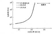
图15示出测量In-B-O膜的电阻率随着时间的改变的结果。在宽组成范围(元素比率B/(In+B)为0.05至0.5的范围)上在基于In-B-O的薄膜中未观测到电阻率随时间的改变。此外,图2示出在其它材料中电阻率随时间的改变的比较。以与In-B-O膜相同方式而形成的In-Zn-O膜和In-Sn-O膜展现出的趋势是,随时间而减少电阻率。这些结果证明了In-B-O膜具有出众的环境稳定性。FIG. 15 shows the results of measuring the change in resistivity with time of the In-B-O film. No change in resistivity over time was observed in In-B-O-based thin films over a wide composition range (element ratio B/(In+B) ranging from 0.05 to 0.5). Furthermore, Figure 2 shows a comparison of the change in resistivity over time in other materials. The In-Zn-O film and the In-Sn-O film formed in the same manner as the In-B-O film exhibit a tendency to decrease the resistivity with time. These results demonstrate the superior environmental stability of In-B-O films.
接下来,检查具有In-B-O膜作为n沟道层的场效应晶体管(FET)的特性以及组成依赖性。晶体管具有图8C所示的底栅结构。具体地说,In-B-O组成分级膜形成在具有热氧化物膜的Si基板上,然后刻图和电极形成被执行,由此在单个基板上形成包括具有彼此不同的组成的活性层的器件。在器件形成之后,在大气中在300℃执行退火工艺。很多FET制造在3英寸晶片上,并且关于特性而被评估。FET具有对于栅极电极使用n+-Si、对于绝缘层使用SiO2并且对于源极电极和漏极电极使用Au/Ti的底栅型顶部接触结构。沟道层宽度和沟道层长度分别是150μm和10μm。在FET评估中使用的源-漏电压是6V。Next, characteristics and composition dependence of a field effect transistor (FET) having an In-BO film as an n-channel layer were examined. The transistor has a bottom gate structure as shown in Fig. 8C. Specifically, an In-BO composition graded film was formed on a Si substrate having a thermal oxide film, and then patterning and electrode formation were performed, thereby forming a device including active layers having mutually different compositions on a single substrate. After the device was formed, an annealing process was performed at 300° C. in the atmosphere. Many FETs were fabricated on 3-inch wafers and evaluated for characteristics. The FET has a bottom gate type top contact structure using n+ -Si for a gate electrode, SiO2 for an insulating layer, and Au/Ti for a source electrode and a drain electrode. The channel layer width and channel layer length were 150 μm and 10 μm, respectively. The source-drain voltage used in the FET evaluation was 6V.
在TFT特性评估中,根据Id1/2(Id:漏极电流)相对于栅极电压(Vg)的斜率获得电子迁移率,并且根据最大Id值与最小Id值的比率获得电流通/断比率。当相对于Vg绘制Id1/2时关于Vg轴的截距被取作阈值电压,以及dVg/d(log Id)的最小值取作S值(将电流增加一个数量级所需的电压值)。In TFT characteristic evaluation, the electron mobility is obtained from the slope of Id1/2 (Id: drain current) with respect to the gate voltage (Vg), and the current on/off ratio is obtained from the ratio of the maximum Id value to the minimum Id value . The intercept on the Vg axis when Id1/2 is plotted against Vg is taken as the threshold voltage, and the minimum value of dVg/d(log Id) is taken as the S value (voltage value required to increase the current by one order of magnitude).
通过评估基板上各个位置处的TFT特性来检查TFT特性相对于元素比率B/(In+B)的改变。结果发现,TFT特性根据基板上的位置(即元素比率B/(In+B))而变化。图4示出各种组成中的Id-Vg特性。Changes in TFT characteristics with respect to the element ratio B/(In+B) were examined by evaluating the TFT characteristics at various positions on the substrate. As a result, it was found that TFT characteristics vary depending on the position on the substrate (ie, the element ratio B/(In+B)). FIG. 4 shows Id-Vg characteristics in various compositions.
在富铟的组成的情况下(例如图4的(A)),导通电流大,以及关断电流相对大。可以使用具有富铟的组成的器件,以用于需要大的导通电流的用途。当应用具有小于图4的(A)的情况的元素比率B/(In+B)的膜时,阈值为负数。In the case of an indium-rich composition (for example, (A) of FIG. 4 ), the on-current is large, and the off-current is relatively large. Devices with indium-rich compositions can be used for applications requiring large on-currents. When a film having an element ratio B/(In+B) smaller than the case of (A) of FIG. 4 is applied, the threshold value is a negative number.
与之对照,在富硼的组成的情况下(例如图4的(C)或(D)),导通电流相对小,但是阈值电压为正数,因此获得″常断特性″。可以使用具有富硼的组成的器件,以用于需要小的关断电流的用途。In contrast, in the case of a boron-rich composition (for example, (C) or (D) of FIG. 4 ), the on-current is relatively small, but the threshold voltage is positive, and thus "normally-off characteristics" are obtained. Devices with boron-rich compositions can be used for applications requiring small off currents.
图4的(B)的情况下的器件展现出最优异的特性。图1还单独示出该器件(图4的(B))的特性。如图1所示,在具有0.16的元素比率B/(In+B)的器件(图4的(B))的情况下,可以获得等于或大于十个数量级的通/断比率。S值是0.4V/decade,场效应迁移率是3cm2/Vs,阈值是4V。The device in the case of (B) of FIG. 4 exhibited the most excellent characteristics. FIG. 1 also separately shows the characteristics of the device ((B) of FIG. 4 ). As shown in FIG. 1 , in the case of a device ((B) of FIG. 4 ) having an element ratio B/(In+B) of 0.16, an on/off ratio equal to or greater than ten orders of magnitude can be obtained. The S value is 0.4V/decade, the field effect mobility is 3cm2 /Vs, and the threshold is 4V.
图5示出场效应迁移率的元素比率B/(In+B)依赖性。可见,场效应迁移率随硼含量减少而增加。当元素比率B/(In+B)为等于或小于0.29时,获得等于或大于0.05cm2/Vs的场效应迁移率。此外,当元素比率B/(In+B)为等于或小于0.22时,获得等于或大于0.1cm2/Vs的场效应迁移率,而当元素比率B/(In+B)为等于或小于0.2时,获得等于或大于1cm2/Vs的场效应迁移率。FIG. 5 shows the element ratio B/(In+B) dependence of field-effect mobility. It can be seen that the field effect mobility increases with the decrease of boron content. When the element ratio B/(In+B) is equal to or less than 0.29, field effect mobility equal to or greater than 0.05 cm2 /Vs is obtained. Furthermore, when the element ratio B/(In+B) is equal to or less than 0.22, field-effect mobility equal to or greater than 0.1 cm2 /Vs is obtained, while when the element ratio B/(In+B) is equal to or less than 0.2 , a field-effect mobility equal to or greater than 1 cm2 /Vs is obtained.
此外,图6示出阈值电压的元素比率B/(In+B)依赖性。通常,当薄膜晶体管的阈值电压Vth是等于或大于0V时,容易构建电路。从图6可见,当元素比率B/(In+B)是等于或大于0.1时,Vth变为正数。In addition, FIG. 6 shows the element ratio B/(In+B) dependence of the threshold voltage. In general, when the threshold voltage Vth of the thin film transistor is equal to or greater than 0V, it is easy to construct a circuit. It can be seen from FIG. 6 that when the element ratio B/(In+B) is equal to or greater than 0.1, Vth becomes a positive number.
图7示出S值的元素比率B/(In+B)依赖性。从图7显而易见,当元素比率B/(In+B)等于或大于0.12并且等于或小于0.2时,获得小S值,这是期望的。FIG. 7 shows the element ratio B/(In+B) dependence of the S value. As apparent from FIG. 7 , when the element ratio B/(In+B) is equal to or greater than 0.12 and equal to or less than 0.2, a small S value is obtained, which is desirable.
在图3A和图3B中,In-Ga-O应用于沟道层的晶体管的特性与In-Al-O应用于沟道层的晶体管的特性进行比较。In-Ga-O应用于沟道层的晶体管的样本以及In-Al-O应用于沟道层的晶体管的样本被制造并且评估,如在上述In-B-O应用于沟道层的晶体管情况下那样。在具有In与Ga之间各种组成比率的各器件(具有In与Al或Ga之间的各种组成比率的各器件)之中,挑选出展现优异晶体管特性的器件。图3A和图3B示出待比较的晶体管特性。如图3A所示,在作为III族元素的B(硼)、Al和Ga之一与In的组合中,In-B-O展现出最大通/断比率。从图3B显而易见,当使用In-B-O时,可以实现具有最小S值的晶体管。因此,显而易见,在使用两种金属元素的非晶氧化物半导体之中,In-B-O作为TFT的沟道材料是优异的。In FIGS. 3A and 3B , characteristics of a transistor in which In-Ga-O is applied to a channel layer are compared with characteristics of a transistor in which In-Al-O is applied to the channel layer. Samples of transistors in which In-Ga-O was applied to the channel layer and samples of transistors in which In-Al-O was applied to the channel layer were fabricated and evaluated as in the case of the above-mentioned transistors in which In-B-O was applied to the channel layer . Among devices having various composition ratios between In and Ga (devices having various composition ratios between In and Al or Ga), devices exhibiting excellent transistor characteristics were selected. 3A and 3B show transistor characteristics to be compared. As shown in FIG. 3A , in a combination of one of B (boron), Al, and Ga, which are group III elements, and In, In—B—O exhibits the largest on/off ratio. It is evident from FIG. 3B that when In-B-O is used, a transistor with a minimum S value can be realized. Therefore, it is apparent that, among amorphous oxide semiconductors using two metal elements, In—B—O is excellent as a channel material of TFT.
示例3Example 3
在该示例中,制造非晶In-Zn-B-O氧化物半导体应用于沟道层的TFT器件。TFT具有图8B所示的结构。In this example, a TFT device in which an amorphous In-Zn-B-O oxide semiconductor was applied to a channel layer was manufactured. The TFT has the structure shown in Fig. 8B.
制备聚对苯二甲酸乙二醇酯(polyethylene terephthalate,PET)膜作为基板。晶体管的沟道长度和沟道宽度分别是60μm和180μm。A polyethylene terephthalate (PET) film was prepared as a substrate. The channel length and channel width of the transistor were 60 μm and 180 μm, respectively.
首先,在该PET基板10上,通过光刻和剥离方法形成栅极电极15,并且栅绝缘层12被形成和刻图。First, on the
栅极电极15以厚度50nm的Mo膜制成。栅绝缘层12是通过溅射为具有150nm厚度而淀积的SiOx膜。SiOx膜的具体介电常数是大约3.7。The
接下来,晶体管的沟道层通过溅射而被形成,并且通过光刻和剥离方法而被刻图。沟道层以基于In-Zn-B-O的非晶氧化物制成,其以组成比率In∶Zn∶B=4∶6∶1而包含In、Zn和B。Next, the channel layer of the transistor is formed by sputtering and patterned by photolithography and lift-off methods. The channel layer was made of an In-Zn-B-O-based amorphous oxide containing In, Zn, and B at a composition ratio of In:Zn:B=4:6:1.
基于In-Zn-B-O的非晶氧化物在氩气和氧气的混合气氛中通过射频溅射而被形成。The In-Zn-B-O-based amorphous oxide was formed by radio frequency sputtering in a mixed atmosphere of argon and oxygen.
在该示例中,三个靶(材料源)用于通过同时淀积来形成膜。三个靶分别是In2O3、B2O3和ZnO的2英寸大小的烧结材料。通过分别控制用于这些靶的输入RF功率,获得具有期望In∶Zn∶B组成比率的氧化物薄膜。气氛被设置为:总压力0.5Pa、气体流率比率Ar∶O2=100∶1。基板温度设置为25℃。In this example, three targets (material sources) were used to form a film by simultaneous deposition. The three targets were 2 inch sintered materials of In2 O3 , B2 O3 and ZnO, respectively. By individually controlling the input RF power for these targets, oxide thin films with desired In:Zn:B composition ratios were obtained. The atmosphere was set as: total pressure 0.5 Pa, gas flow rate ratio Ar:O2 =100:1. The substrate temperature was set to 25 °C.
发现因此而形成的氧化物膜是非晶膜,因为在X射线衍射(薄膜方法,入射角0.5°)中并未检测到明显衍射峰。非晶氧化物膜的厚度大约是30nm。The oxide film thus formed was found to be an amorphous film because no clear diffraction peak was detected in X-ray diffraction (thin film method, incident angle 0.5°). The thickness of the amorphous oxide film is about 30 nm.
光学吸收谱分析表明,所形成的非晶氧化物膜具有大约3eV的禁带能量宽度,并且对于可见光是透明的。Optical absorption spectrum analysis showed that the formed amorphous oxide film had a bandgap energy width of about 3 eV and was transparent to visible light.
源极电极、漏极电极和栅极电极以包括In2O3∶Sn的透明导电膜制成,每一电极具有100nm的厚度。The source electrode, drain electrode, and gate electrode were made of a transparent conductive film including In2 O3 :Sn, each having a thickness of 100 nm.
因此而制造的TFT关于特性而被评估。The TFTs thus manufactured were evaluated with respect to characteristics.
在室温测量并且评估的PET膜上形成的该示例的晶体管的通/断比率超过109。计算出的场效应迁移率大约是5cm2/Vs。The on/off ratio of the transistor of this example formed on the PET film measured and evaluated at room temperature exceeded 109 . The calculated field effect mobility is about 5 cm2 /Vs.
此外,根据该示例的对于沟道采用In-Zn-B-O的薄膜晶体管具有高性能和高环境稳定性。Furthermore, the thin film transistor employing In-Zn-B-O for the channel according to this example has high performance and high environmental stability.
当非晶氧化物材料的元素比率B/(In+Zn+B)是等于或大于0.05并且等于或小于0.29时,优异的晶体管操作被确保。When the element ratio B/(In+Zn+B) of the amorphous oxide material is equal to or greater than 0.05 and equal to or less than 0.29, excellent transistor operation is ensured.
与使用不含B的In-Zn-O作为沟道的薄膜晶体管相比,使用基于In-Zn-B-O的氧化物半导体作为沟道的该示例的薄膜晶体管在环境稳定性方面也得到改进(在大气中存储期间的特性波动小)。The thin film transistor of this example using an In-Zn-B-O-based oxide semiconductor as a channel is also improved in environmental stability compared to a thin film transistor using In-Zn-O not containing B as a channel (in Small fluctuations in properties during storage in the atmosphere).
虽然已经参照示例性实施例描述了本发明,但应理解,本发明不限于所公开的示例性实施例。所附权利要求的范围与最宽泛的解释一致,从而包括所有这样的修改和等同结构及功能。While the present invention has been described with reference to exemplary embodiments, it is to be understood that the invention is not limited to the disclosed exemplary embodiments. The scope of the appended claims is to be accorded the broadest interpretation thereby including all such modifications and equivalent structures and functions.
本申请要求2008年1月23日提交的日本专利申请No.2008-012592的权益,其在此全部引入作为参考。This application claims the benefit of Japanese Patent Application No. 2008-012592 filed on January 23, 2008, which is hereby incorporated by reference in its entirety.
Claims (10)
Translated fromChineseApplications Claiming Priority (3)
| Application Number | Priority Date | Filing Date | Title |
|---|---|---|---|
| JP2008012592AJP5219529B2 (en) | 2008-01-23 | 2008-01-23 | Field effect transistor and display device including the field effect transistor |
| JP2008-012592 | 2008-01-23 | ||
| PCT/JP2009/051144WO2009093724A1 (en) | 2008-01-23 | 2009-01-20 | Field-effect transistor using amorphous oxide |
Publications (2)
| Publication Number | Publication Date |
|---|---|
| CN101926008A CN101926008A (en) | 2010-12-22 |
| CN101926008Btrue CN101926008B (en) | 2012-08-29 |
Family
ID=40599920
Family Applications (1)
| Application Number | Title | Priority Date | Filing Date |
|---|---|---|---|
| CN2009801030020AExpired - Fee RelatedCN101926008B (en) | 2008-01-23 | 2009-01-20 | Field Effect Transistor Using Amorphous Oxide |
Country Status (7)
| Country | Link |
|---|---|
| US (1) | US8314425B2 (en) |
| EP (1) | EP2243164B1 (en) |
| JP (1) | JP5219529B2 (en) |
| KR (1) | KR101186858B1 (en) |
| CN (1) | CN101926008B (en) |
| TW (1) | TWI405334B (en) |
| WO (1) | WO2009093724A1 (en) |
Families Citing this family (16)
| Publication number | Priority date | Publication date | Assignee | Title |
|---|---|---|---|---|
| EP2453481B1 (en) | 2004-11-10 | 2017-01-11 | Canon Kabushiki Kaisha | Field effect transistor with amorphous oxide |
| CN102598283B (en)* | 2009-09-04 | 2016-05-18 | 株式会社半导体能源研究所 | Semiconductor device and manufacturing method thereof |
| WO2011027701A1 (en)* | 2009-09-04 | 2011-03-10 | Semiconductor Energy Laboratory Co., Ltd. | Light-emitting device and method for manufacturing the same |
| KR102162746B1 (en)* | 2009-10-21 | 2020-10-07 | 가부시키가이샤 한도오따이 에네루기 켄큐쇼 | Analog circuit and semiconductor device |
| KR101490726B1 (en) | 2009-10-21 | 2015-02-09 | 가부시키가이샤 한도오따이 에네루기 켄큐쇼 | Semiconductor device |
| CN105702688B (en)* | 2009-10-21 | 2020-09-08 | 株式会社半导体能源研究所 | Liquid crystal display device and electronic apparatus including the same |
| SG10201406869QA (en)* | 2009-10-29 | 2014-12-30 | Semiconductor Energy Lab | Semiconductor device |
| KR101893332B1 (en) | 2009-11-13 | 2018-08-31 | 가부시키가이샤 한도오따이 에네루기 켄큐쇼 | Semiconductor device and driving method thereof |
| KR102719739B1 (en)* | 2009-12-04 | 2024-10-21 | 가부시키가이샤 한도오따이 에네루기 켄큐쇼 | Semiconductor device |
| KR102352590B1 (en)* | 2009-12-18 | 2022-01-17 | 가부시키가이샤 한도오따이 에네루기 켄큐쇼 | Liquid crystal display device and electronic device |
| CN103985760B (en) | 2009-12-25 | 2017-07-18 | 株式会社半导体能源研究所 | Semiconductor device |
| JP2014142986A (en) | 2012-12-26 | 2014-08-07 | Semiconductor Energy Lab Co Ltd | Semiconductor device |
| KR20140106977A (en)* | 2013-02-27 | 2014-09-04 | 삼성전자주식회사 | Metal oxide semiconductor Thin Film Transistors having high performance and methods of manufacturing the same |
| US9112460B2 (en)* | 2013-04-05 | 2015-08-18 | Semiconductor Energy Laboratory Co., Ltd. | Signal processing device |
| US9899457B2 (en)* | 2015-04-24 | 2018-02-20 | Universal Display Corporation | Flexible OLED display having increased lifetime |
| US20210343876A1 (en)* | 2018-08-01 | 2021-11-04 | Idemitsu Kosan Co.,Ltd. | Crystal structure compound, oxide sintered body, sputtering target, crystalline oxide thin film, amorphous oxide thin film, thin film transistor and electronic equipment |
Family Cites Families (31)
| Publication number | Priority date | Publication date | Assignee | Title |
|---|---|---|---|---|
| JP3205167B2 (en) | 1993-04-05 | 2001-09-04 | キヤノン株式会社 | Method of manufacturing electron source and method of manufacturing image forming apparatus |
| TW297142B (en)* | 1993-09-20 | 1997-02-01 | Handotai Energy Kenkyusho Kk | |
| JP2946189B2 (en) | 1994-10-17 | 1999-09-06 | キヤノン株式会社 | Electron source, image forming apparatus, and activation method thereof |
| US6231412B1 (en) | 1996-09-18 | 2001-05-15 | Canon Kabushiki Kaisha | Method of manufacturing and adjusting electron source array |
| WO2002016679A1 (en)* | 2000-08-18 | 2002-02-28 | Tohoku Techno Arch Co., Ltd. | Polycrystalline semiconductor material and method of manufacture thereof |
| US6936854B2 (en) | 2001-05-10 | 2005-08-30 | Canon Kabushiki Kaisha | Optoelectronic substrate |
| JP3833131B2 (en) | 2002-03-25 | 2006-10-11 | キヤノン株式会社 | Optical transmission equipment |
| US7189992B2 (en) | 2002-05-21 | 2007-03-13 | State Of Oregon Acting By And Through The Oregon State Board Of Higher Education On Behalf Of Oregon State University | Transistor structures having a transparent channel |
| US7145174B2 (en) | 2004-03-12 | 2006-12-05 | Hewlett-Packard Development Company, Lp. | Semiconductor device |
| US7242039B2 (en) | 2004-03-12 | 2007-07-10 | Hewlett-Packard Development Company, L.P. | Semiconductor device |
| US7297977B2 (en) | 2004-03-12 | 2007-11-20 | Hewlett-Packard Development Company, L.P. | Semiconductor device |
| CN1998087B (en)* | 2004-03-12 | 2014-12-31 | 独立行政法人科学技术振兴机构 | Amorphous oxide and thin film transistor |
| US7282782B2 (en) | 2004-03-12 | 2007-10-16 | Hewlett-Packard Development Company, L.P. | Combined binary oxide semiconductor device |
| JP4544518B2 (en) | 2004-09-01 | 2010-09-15 | キヤノン株式会社 | Electric field excitation type light emitting device and image display device |
| US7863611B2 (en) | 2004-11-10 | 2011-01-04 | Canon Kabushiki Kaisha | Integrated circuits utilizing amorphous oxides |
| JP5126730B2 (en)* | 2004-11-10 | 2013-01-23 | キヤノン株式会社 | Method for manufacturing field effect transistor |
| US7829444B2 (en)* | 2004-11-10 | 2010-11-09 | Canon Kabushiki Kaisha | Field effect transistor manufacturing method |
| JP4560502B2 (en) | 2005-09-06 | 2010-10-13 | キヤノン株式会社 | Field effect transistor |
| JP5006598B2 (en) | 2005-09-16 | 2012-08-22 | キヤノン株式会社 | Field effect transistor |
| JP5395994B2 (en)* | 2005-11-18 | 2014-01-22 | 出光興産株式会社 | Semiconductor thin film, manufacturing method thereof, and thin film transistor |
| JP5376750B2 (en)* | 2005-11-18 | 2013-12-25 | 出光興産株式会社 | Semiconductor thin film, manufacturing method thereof, thin film transistor, active matrix drive display panel |
| JP5177954B2 (en) | 2006-01-30 | 2013-04-10 | キヤノン株式会社 | Field effect transistor |
| JP5110803B2 (en) | 2006-03-17 | 2012-12-26 | キヤノン株式会社 | FIELD EFFECT TRANSISTOR USING OXIDE FILM FOR CHANNEL AND METHOD FOR MANUFACTURING THE SAME |
| JP5294565B2 (en) | 2006-03-17 | 2013-09-18 | キヤノン株式会社 | Light emitting device and method for manufacturing light emitting device |
| US20080001538A1 (en) | 2006-06-29 | 2008-01-03 | Cok Ronald S | Led device having improved light output |
| JP4332545B2 (en) | 2006-09-15 | 2009-09-16 | キヤノン株式会社 | Field effect transistor and manufacturing method thereof |
| JP5116290B2 (en) | 2006-11-21 | 2013-01-09 | キヤノン株式会社 | Thin film transistor manufacturing method |
| JP5244331B2 (en) | 2007-03-26 | 2013-07-24 | 出光興産株式会社 | Amorphous oxide semiconductor thin film, manufacturing method thereof, thin film transistor manufacturing method, field effect transistor, light emitting device, display device, and sputtering target |
| CN101663762B (en) | 2007-04-25 | 2011-09-21 | 佳能株式会社 | Oxynitride semiconductor |
| JP5213429B2 (en) | 2007-12-13 | 2013-06-19 | キヤノン株式会社 | Field effect transistor |
| JP5451280B2 (en) | 2008-10-09 | 2014-03-26 | キヤノン株式会社 | Wurtzite crystal growth substrate, manufacturing method thereof, and semiconductor device |
- 2008
- 2008-01-23JPJP2008012592Apatent/JP5219529B2/ennot_activeExpired - Fee Related
- 2009
- 2009-01-20USUS12/747,601patent/US8314425B2/ennot_activeExpired - Fee Related
- 2009-01-20KRKR1020107017793Apatent/KR101186858B1/ennot_activeExpired - Fee Related
- 2009-01-20CNCN2009801030020Apatent/CN101926008B/ennot_activeExpired - Fee Related
- 2009-01-20EPEP09704795.5Apatent/EP2243164B1/ennot_activeNot-in-force
- 2009-01-20WOPCT/JP2009/051144patent/WO2009093724A1/enactiveApplication Filing
- 2009-01-21TWTW098102305Apatent/TWI405334B/ennot_activeIP Right Cessation
Also Published As
| Publication number | Publication date |
|---|---|
| US8314425B2 (en) | 2012-11-20 |
| EP2243164B1 (en) | 2017-08-30 |
| JP2009176864A (en) | 2009-08-06 |
| KR20100102709A (en) | 2010-09-24 |
| CN101926008A (en) | 2010-12-22 |
| TW201001701A (en) | 2010-01-01 |
| EP2243164A1 (en) | 2010-10-27 |
| TWI405334B (en) | 2013-08-11 |
| WO2009093724A1 (en) | 2009-07-30 |
| JP5219529B2 (en) | 2013-06-26 |
| US20100264419A1 (en) | 2010-10-21 |
| KR101186858B1 (en) | 2012-10-02 |
Similar Documents
| Publication | Publication Date | Title |
|---|---|---|
| CN101926008B (en) | Field Effect Transistor Using Amorphous Oxide | |
| US8188471B2 (en) | Field effect transistor | |
| JP5213429B2 (en) | Field effect transistor | |
| CN101933150B (en) | Thin film transistor using an oxide semiconductor and display | |
| US8212248B2 (en) | Amorphous oxide and field effect transistor | |
| KR100973124B1 (en) | Field effect transistor having a channel with an oxide semiconductor material comprising indium and zinc | |
| US7906780B2 (en) | Field effect transistor | |
| CN101401213A (en) | Field effect transistor using oxide film for channel and manufacturing method thereof | |
| CN101258607A (en) | Field-effect transistor using amorphous oxide film as channel layer, method for manufacturing field-effect transistor using amorphous oxide film as channel layer, and method for manufacturing amorphous oxide film |
Legal Events
| Date | Code | Title | Description |
|---|---|---|---|
| C06 | Publication | ||
| PB01 | Publication | ||
| C10 | Entry into substantive examination | ||
| SE01 | Entry into force of request for substantive examination | ||
| C14 | Grant of patent or utility model | ||
| GR01 | Patent grant | ||
| CF01 | Termination of patent right due to non-payment of annual fee | Granted publication date:20120829 | |
| CF01 | Termination of patent right due to non-payment of annual fee |