CN101903974A - Method for manufacturing thin film laminated device, method for manufacturing display device, and thin film laminated device - Google Patents
Method for manufacturing thin film laminated device, method for manufacturing display device, and thin film laminated deviceDownload PDFInfo
- Publication number
- CN101903974A CN101903974ACN2008801214975ACN200880121497ACN101903974ACN 101903974 ACN101903974 ACN 101903974ACN 2008801214975 ACN2008801214975 ACN 2008801214975ACN 200880121497 ACN200880121497 ACN 200880121497ACN 101903974 ACN101903974 ACN 101903974A
- Authority
- CN
- China
- Prior art keywords
- film
- inoranic membrane
- substrate
- thin film
- plastic base
- Prior art date
- Legal status (The legal status is an assumption and is not a legal conclusion. Google has not performed a legal analysis and makes no representation as to the accuracy of the status listed.)
- Granted
Links
Images


Classifications
- H—ELECTRICITY
- H10—SEMICONDUCTOR DEVICES; ELECTRIC SOLID-STATE DEVICES NOT OTHERWISE PROVIDED FOR
- H10D—INORGANIC ELECTRIC SEMICONDUCTOR DEVICES
- H10D86/00—Integrated devices formed in or on insulating or conducting substrates, e.g. formed in silicon-on-insulator [SOI] substrates or on stainless steel or glass substrates
- H10D86/01—Manufacture or treatment
- H10D86/021—Manufacture or treatment of multiple TFTs
- H10D86/0214—Manufacture or treatment of multiple TFTs using temporary substrates
- H—ELECTRICITY
- H01—ELECTRIC ELEMENTS
- H01L—SEMICONDUCTOR DEVICES NOT COVERED BY CLASS H10
- H01L21/00—Processes or apparatus adapted for the manufacture or treatment of semiconductor or solid state devices or of parts thereof
- H01L21/67—Apparatus specially adapted for handling semiconductor or electric solid state devices during manufacture or treatment thereof; Apparatus specially adapted for handling wafers during manufacture or treatment of semiconductor or electric solid state devices or components ; Apparatus not specifically provided for elsewhere
- H01L21/683—Apparatus specially adapted for handling semiconductor or electric solid state devices during manufacture or treatment thereof; Apparatus specially adapted for handling wafers during manufacture or treatment of semiconductor or electric solid state devices or components ; Apparatus not specifically provided for elsewhere for supporting or gripping
- H01L21/6835—Apparatus specially adapted for handling semiconductor or electric solid state devices during manufacture or treatment thereof; Apparatus specially adapted for handling wafers during manufacture or treatment of semiconductor or electric solid state devices or components ; Apparatus not specifically provided for elsewhere for supporting or gripping using temporarily an auxiliary support
- H—ELECTRICITY
- H10—SEMICONDUCTOR DEVICES; ELECTRIC SOLID-STATE DEVICES NOT OTHERWISE PROVIDED FOR
- H10D—INORGANIC ELECTRIC SEMICONDUCTOR DEVICES
- H10D30/00—Field-effect transistors [FET]
- H10D30/60—Insulated-gate field-effect transistors [IGFET]
- H10D30/67—Thin-film transistors [TFT]
- H10D30/6758—Thin-film transistors [TFT] characterised by the insulating substrates
- H—ELECTRICITY
- H10—SEMICONDUCTOR DEVICES; ELECTRIC SOLID-STATE DEVICES NOT OTHERWISE PROVIDED FOR
- H10D—INORGANIC ELECTRIC SEMICONDUCTOR DEVICES
- H10D86/00—Integrated devices formed in or on insulating or conducting substrates, e.g. formed in silicon-on-insulator [SOI] substrates or on stainless steel or glass substrates
- H10D86/40—Integrated devices formed in or on insulating or conducting substrates, e.g. formed in silicon-on-insulator [SOI] substrates or on stainless steel or glass substrates characterised by multiple TFTs
- H10D86/411—Integrated devices formed in or on insulating or conducting substrates, e.g. formed in silicon-on-insulator [SOI] substrates or on stainless steel or glass substrates characterised by multiple TFTs characterised by materials, geometry or structure of the substrates
- H—ELECTRICITY
- H10—SEMICONDUCTOR DEVICES; ELECTRIC SOLID-STATE DEVICES NOT OTHERWISE PROVIDED FOR
- H10D—INORGANIC ELECTRIC SEMICONDUCTOR DEVICES
- H10D86/00—Integrated devices formed in or on insulating or conducting substrates, e.g. formed in silicon-on-insulator [SOI] substrates or on stainless steel or glass substrates
- H10D86/40—Integrated devices formed in or on insulating or conducting substrates, e.g. formed in silicon-on-insulator [SOI] substrates or on stainless steel or glass substrates characterised by multiple TFTs
- H10D86/60—Integrated devices formed in or on insulating or conducting substrates, e.g. formed in silicon-on-insulator [SOI] substrates or on stainless steel or glass substrates characterised by multiple TFTs wherein the TFTs are in active matrices
- H—ELECTRICITY
- H01—ELECTRIC ELEMENTS
- H01L—SEMICONDUCTOR DEVICES NOT COVERED BY CLASS H10
- H01L2221/00—Processes or apparatus adapted for the manufacture or treatment of semiconductor or solid state devices or of parts thereof covered by H01L21/00
- H01L2221/67—Apparatus for handling semiconductor or electric solid state devices during manufacture or treatment thereof; Apparatus for handling wafers during manufacture or treatment of semiconductor or electric solid state devices or components; Apparatus not specifically provided for elsewhere
- H01L2221/683—Apparatus for handling semiconductor or electric solid state devices during manufacture or treatment thereof; Apparatus for handling wafers during manufacture or treatment of semiconductor or electric solid state devices or components; Apparatus not specifically provided for elsewhere for supporting or gripping
- H01L2221/68304—Apparatus for handling semiconductor or electric solid state devices during manufacture or treatment thereof; Apparatus for handling wafers during manufacture or treatment of semiconductor or electric solid state devices or components; Apparatus not specifically provided for elsewhere for supporting or gripping using temporarily an auxiliary support
- H01L2221/6835—Apparatus for handling semiconductor or electric solid state devices during manufacture or treatment thereof; Apparatus for handling wafers during manufacture or treatment of semiconductor or electric solid state devices or components; Apparatus not specifically provided for elsewhere for supporting or gripping using temporarily an auxiliary support used as a support during build up manufacturing of active devices
- H—ELECTRICITY
- H10—SEMICONDUCTOR DEVICES; ELECTRIC SOLID-STATE DEVICES NOT OTHERWISE PROVIDED FOR
- H10D—INORGANIC ELECTRIC SEMICONDUCTOR DEVICES
- H10D30/00—Field-effect transistors [FET]
- H10D30/60—Insulated-gate field-effect transistors [IGFET]
- H10D30/67—Thin-film transistors [TFT]
- H10D30/674—Thin-film transistors [TFT] characterised by the active materials
- H10D30/6755—Oxide semiconductors, e.g. zinc oxide, copper aluminium oxide or cadmium stannate
- Y—GENERAL TAGGING OF NEW TECHNOLOGICAL DEVELOPMENTS; GENERAL TAGGING OF CROSS-SECTIONAL TECHNOLOGIES SPANNING OVER SEVERAL SECTIONS OF THE IPC; TECHNICAL SUBJECTS COVERED BY FORMER USPC CROSS-REFERENCE ART COLLECTIONS [XRACs] AND DIGESTS
- Y10—TECHNICAL SUBJECTS COVERED BY FORMER USPC
- Y10T—TECHNICAL SUBJECTS COVERED BY FORMER US CLASSIFICATION
- Y10T156/00—Adhesive bonding and miscellaneous chemical manufacture
- Y10T156/10—Methods of surface bonding and/or assembly therefor
- Y10T156/1052—Methods of surface bonding and/or assembly therefor with cutting, punching, tearing or severing
- Y10T156/1062—Prior to assembly
- Y10T156/1064—Partial cutting [e.g., grooving or incising]
- Y—GENERAL TAGGING OF NEW TECHNOLOGICAL DEVELOPMENTS; GENERAL TAGGING OF CROSS-SECTIONAL TECHNOLOGIES SPANNING OVER SEVERAL SECTIONS OF THE IPC; TECHNICAL SUBJECTS COVERED BY FORMER USPC CROSS-REFERENCE ART COLLECTIONS [XRACs] AND DIGESTS
- Y10—TECHNICAL SUBJECTS COVERED BY FORMER USPC
- Y10T—TECHNICAL SUBJECTS COVERED BY FORMER US CLASSIFICATION
- Y10T156/00—Adhesive bonding and miscellaneous chemical manufacture
- Y10T156/11—Methods of delaminating, per se; i.e., separating at bonding face
- Y10T156/1168—Gripping and pulling work apart during delaminating
- Y10T156/1189—Gripping and pulling work apart during delaminating with shearing during delaminating
- Y—GENERAL TAGGING OF NEW TECHNOLOGICAL DEVELOPMENTS; GENERAL TAGGING OF CROSS-SECTIONAL TECHNOLOGIES SPANNING OVER SEVERAL SECTIONS OF THE IPC; TECHNICAL SUBJECTS COVERED BY FORMER USPC CROSS-REFERENCE ART COLLECTIONS [XRACs] AND DIGESTS
- Y10—TECHNICAL SUBJECTS COVERED BY FORMER USPC
- Y10T—TECHNICAL SUBJECTS COVERED BY FORMER US CLASSIFICATION
- Y10T156/00—Adhesive bonding and miscellaneous chemical manufacture
- Y10T156/11—Methods of delaminating, per se; i.e., separating at bonding face
- Y10T156/1168—Gripping and pulling work apart during delaminating
- Y10T156/1195—Delaminating from release surface
- Y—GENERAL TAGGING OF NEW TECHNOLOGICAL DEVELOPMENTS; GENERAL TAGGING OF CROSS-SECTIONAL TECHNOLOGIES SPANNING OVER SEVERAL SECTIONS OF THE IPC; TECHNICAL SUBJECTS COVERED BY FORMER USPC CROSS-REFERENCE ART COLLECTIONS [XRACs] AND DIGESTS
- Y10—TECHNICAL SUBJECTS COVERED BY FORMER USPC
- Y10T—TECHNICAL SUBJECTS COVERED BY FORMER US CLASSIFICATION
- Y10T428/00—Stock material or miscellaneous articles
- Y10T428/31504—Composite [nonstructural laminate]
Landscapes
- Engineering & Computer Science (AREA)
- Physics & Mathematics (AREA)
- Condensed Matter Physics & Semiconductors (AREA)
- General Physics & Mathematics (AREA)
- Manufacturing & Machinery (AREA)
- Computer Hardware Design (AREA)
- Microelectronics & Electronic Packaging (AREA)
- Power Engineering (AREA)
- Liquid Crystal (AREA)
- Thin Film Transistor (AREA)
Abstract
Translated fromChinese
Description
Translated fromChinese技术领域technical field
本发明涉及薄膜层叠器件的制造方法和显示装置的制造方法、以及薄膜层叠器件。The present invention relates to a method for manufacturing a thin-film laminated device, a method for manufacturing a display device, and a thin-film laminated device.
背景技术Background technique
以往,尝试代替玻璃和硅等较硬的基板,使用塑料和金属薄膜等具有柔软性的基板,制造晶体管和传感器等具有高度性能的薄膜器件。特别是具有透明性、耐久性优良的塑料基板作为用于下一代显示器的基板被高度关注。但是,存在塑料基板与玻璃基板相比较薄且容易弯曲,基板搬运困难的大课题。In the past, attempts have been made to manufacture high-performance thin-film devices such as transistors and sensors by using flexible substrates such as plastic and metal thin films instead of hard substrates such as glass and silicon. In particular, plastic substrates excellent in transparency and durability are attracting attention as substrates for next-generation displays. However, plastic substrates are thinner and more easily bent than glass substrates, and there is a big problem of difficulty in conveying the substrates.
对于与这样的塑料基板相关的问题,例如,专利文献1中,记载有对复合基板进行光刻工序等处理后,通过从背面照射紫外线将塑料基板从支撑基板分离的方法,该复合基板通过使用粘合力会因紫外线而减少的粘合剂将塑料基板贴合到作为支撑基板的玻璃基板而成。此外,专利文献2中,记载有通过加热将塑料基板从支撑基板分离的方法。Regarding the problems related to such plastic substrates, for example, Patent Document 1 describes a method of separating the plastic substrate from the supporting substrate by irradiating ultraviolet light from the back surface after processing such as a photolithography process on the composite substrate. Adhesive whose adhesive force is reduced by ultraviolet rays is made by bonding a plastic substrate to a glass substrate as a supporting substrate. In addition, Patent Document 2 describes a method of separating a plastic substrate from a support substrate by heating.
专利文献1:日本特开平7-325297号公报Patent Document 1: Japanese Patent Application Laid-Open No. 7-325297
专利文献2:日本特开2000-248243号公报Patent Document 2: Japanese Patent Laid-Open No. 2000-248243
发明内容Contents of the invention
但是,在上述方法中,存在如下问题:在复合基板的处理工序中,粘合力在紫外线照射和加热时降低,处理中塑料基板从支撑基板剥离等。该剥离是由于如下原因而产生的:塑料基板和粘合材料(有机材料)的由热和水分吸收导致的基板膨胀与作为无机材料的玻璃基板等支撑基板相比非常大,因其差而在二者的界面产生应力。特别是,在制造高性能的TFT(薄膜晶体管)的情况下,需要在接近250℃的非常高的温度下成膜,或者通过紫外线照射反复制作细微的图案,加热和紫外线照射导致粘合材料的粘合力的降低。因此,在良好地使支撑基板支撑塑料基板的状态下,对塑料基板进行形成薄膜等处理存在折衷的问题(trade-of),在塑料基板上良好地形成器件非常困难。进而,粘合力会因紫外线和热而降低的粘合材料与仅特殊化为高粘合性的粘合材料相比价格非常高,在制造成本方面也存在问题。However, in the above-mentioned method, there are problems such as that the adhesive force is lowered by ultraviolet irradiation and heating during the processing process of the composite substrate, and that the plastic substrate is peeled off from the support substrate during processing, and the like. This delamination occurs due to the fact that the expansion of the substrate due to heat and moisture absorption of the plastic substrate and the adhesive material (organic material) is very large compared with a support substrate such as a glass substrate which is an inorganic material, and it is poor in The interface between the two generates stress. In particular, in the case of manufacturing high-performance TFTs (Thin Film Transistors), it is necessary to form a film at a very high temperature close to 250°C, or to repeatedly create fine patterns by ultraviolet irradiation, and heating and ultraviolet irradiation lead to the deterioration of the adhesive material. Decreased adhesion. Therefore, there is a trade-off in processing such as forming a thin film on the plastic substrate in a state where the support substrate supports the plastic substrate well, and it is very difficult to form devices on the plastic substrate well. Furthermore, an adhesive material whose adhesive force is reduced by ultraviolet rays and heat is very expensive compared with an adhesive material specialized only in high adhesiveness, and there is also a problem in terms of production cost.
本发明是鉴于上述各点而完成的,其目的在于,提供能够以良好的制造成本在塑料基板上良好地形成薄膜器件的薄膜层叠器件和显示装置的制造方法。The present invention has been made in view of the above points, and an object of the present invention is to provide a method for manufacturing a thin-film multilayer device and a display device that can favorably form a thin-film device on a plastic substrate at a favorable manufacturing cost.
本发明的薄膜层叠器件的制造方法是在塑料基板层叠有多层薄膜的薄膜层叠器件的制造方法,包括:第一工序,准备依次层叠有第一无机膜和第二无机膜的塑料基板;第二工序,利用粘合剂从第一无机膜和第二无机膜一侧将塑料基板贴合在支撑基板,使支撑基板以比第一无机膜与第二无机膜之间的粘合力强的粘合力支撑塑料基板;第三工序,在被支撑基板支撑的塑料基板上层叠多层薄膜;和第四工序,通过分离第一无机膜与第二无机膜,将层叠有多层薄膜的塑料基板从支撑基板分离。The method for manufacturing a thin-film laminated device of the present invention is a method for manufacturing a thin-film laminated device with a multilayer thin film laminated on a plastic substrate, comprising: a first step of preparing a plastic substrate on which a first inorganic film and a second inorganic film are laminated in sequence; In the second process, the plastic substrate is bonded to the support substrate from the side of the first inorganic film and the second inorganic film using an adhesive, so that the support substrate is stronger than the adhesive force between the first inorganic film and the second inorganic film. an adhesive force supporting the plastic substrate; a third process of laminating the multilayer film on the plastic substrate supported by the supporting substrate; and a fourth process of separating the plastic laminated with the multilayer film by separating the first inorganic film from the second inorganic film. The substrate is separated from the support substrate.
根据上述结构,能够在使用粘合力强的粘合剂使支撑基板牢固地支撑容易产生弯曲和挠曲的塑料基板的状态下形成多层薄膜。因此,即使在反复进行高温加热和湿式处理等工序的薄膜层叠器件制造中,也能够良好地进行制造处理而塑料基板不会从支撑基板剥离。According to the above structure, it is possible to form a multilayer film in a state where the support substrate firmly supports the plastic substrate, which is prone to bending and warping, using an adhesive having strong adhesive force. Therefore, even in the manufacture of a thin film laminated device in which steps such as high-temperature heating and wet processing are repeated, the manufacturing process can be performed satisfactorily without peeling the plastic substrate from the support substrate.
此外,在塑料基板上形成多层薄膜后,不是从强力粘合的支撑基板直接分离,而是通过分离以弱粘合力粘合的第一无机膜与第二无机膜,将塑料基板从支撑基板分离。因此,不需要粘合性能会因紫外线照射和加热等而降低的高价的粘合材料,此外,不需要紫外线照射和加热所需的处理装置。从而,能够以良好的处理效率和处理成本将塑料基板从支撑基板分离。In addition, after forming a multilayer thin film on a plastic substrate, the plastic substrate is separated from the support substrate by separating the first inorganic film and the second inorganic film that are bonded with weak adhesive force, instead of directly separating from the support substrate that is strongly bonded. Substrate separation. Therefore, an expensive adhesive material whose adhesive performance is lowered by ultraviolet irradiation, heating, etc. is not required, and a processing device required for ultraviolet irradiation and heating is not required. Thus, the plastic substrate can be separated from the support substrate with good processing efficiency and processing cost.
根据本发明,能够以良好的制造成本在塑料基板上良好地形成薄膜器件。According to the present invention, a thin film device can be formed favorably on a plastic substrate at a favorable manufacturing cost.
附图说明Description of drawings
图1表示液晶显示装置的剖视图。FIG. 1 shows a cross-sectional view of a liquid crystal display device.
图2是有源矩阵基板的剖视图。Fig. 2 is a cross-sectional view of an active matrix substrate.
图3是对置基板的剖视图。Fig. 3 is a cross-sectional view of a counter substrate.
图4是依次层叠有SiNx膜、非晶硅膜和ITO膜的塑料基板的剖视图。4 is a cross-sectional view of a plastic substrate on which a SiNx film, an amorphous silicon film, and an ITO film are laminated in this order.
图5是被玻璃基板支撑的塑料基板的剖视图和与其对应的俯视图。5 is a cross-sectional view of a plastic substrate supported by a glass substrate and a corresponding top view thereof.
图6是被玻璃基板支撑且形成有TFT的塑料基板的剖视图。6 is a cross-sectional view of a plastic substrate supported by a glass substrate and on which TFTs are formed.
图7是使SiNx膜与非晶硅膜分离的塑料基板的剖视图。7 is a cross-sectional view of a plastic substrate in which a SiNx film is separated from an amorphous silicon film.
图8是使比截断面靠内侧的SiNx膜从非晶硅膜分离的塑料基板的剖视图。8 is a cross-sectional view of a plastic substrate in which the SiNx film is separated from the amorphous silicon film on the inner side of the cross-section.
符号的说明Explanation of symbols
10液晶显示装置10 liquid crystal display device
13有源矩阵基板13 active matrix substrate
14对置基板14 opposing substrates
16TFT16TFT
19、32塑料基板19, 32 plastic substrate
41SiNx膜(第一无机膜)41SiNx film (first inorganic film)
42非晶硅膜(第二无机膜)42 Amorphous silicon film (second inorganic film)
43ITO膜(第三无机膜)43ITO film (the third inorganic film)
44玻璃基板(支撑基板)44 glass substrate (support substrate)
45粘合剂45 adhesive
50激光50 lasers
51截断面51 section
具体实施方式Detailed ways
以下,基于附图对本发明的实施方式的薄膜层叠器件的制造方法和显示装置的制造方法进行详细说明。另外,本发明不限于以下的实施方式。此外,在本实施方式中,作为显示装置以液晶显示装置为例进行说明。Hereinafter, a method of manufacturing a thin film laminated device and a method of manufacturing a display device according to an embodiment of the present invention will be described in detail with reference to the drawings. In addition, this invention is not limited to the following embodiment. In addition, in this embodiment, a liquid crystal display device will be described as an example of a display device.
(液晶显示装置10的结构)(Structure of Liquid Crystal Display Device 10)
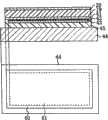
图1表示本发明的实施方式的液晶显示装置10的剖视图。液晶显示装置10由液晶显示面板11和背光源12构成。FIG. 1 shows a cross-sectional view of a liquid
液晶显示装置10包括:分别作为在塑料基板层叠有多层薄膜的薄膜层叠器件的有源矩阵基板13和对置基板14。液晶显示装置10具有在有源矩阵基板13与对置基板14之间形成的液晶层15。The liquid
图2表示有源矩阵基板13的剖视图。在有源矩阵基板13上设置有多个像素(未图示),在各像素上形成有薄膜晶体管(TFT16)。此外,有源矩阵基板13在液晶层15一侧的表面设置有取向膜17,并且在与液晶层15一侧相反的一侧的表面设置有偏光板18。FIG. 2 shows a cross-sectional view of the
有源矩阵基板13包括例如厚度为0.1mm的塑料基板19,塑料基板19由例如环氧树脂、PET树脂、PES树脂、聚酰亚胺树脂、聚酯、聚碳酸酯和聚丙烯酸树脂等的至少一种形成。此外,塑料基板19只要为表现出柔软性的基板即可,也可以为包含玻璃成分等的复合型塑料基板。在塑料基板19的一面上例如以150nm等的厚度形成有SiNx膜20作为底涂层(base coat)。在SiNx膜20的一部分对各个像素(省略图示)以200nm左右的厚度形成有例如由Ti等构成的栅极电极21,以覆盖上述SiNx膜20和栅极电极21的方式例如以400nm左右的厚度形成有由SiNx层等形成的栅极绝缘膜22。The
在栅极绝缘膜22上例如以150nm左右的厚度形成有隔着栅极绝缘膜22覆盖栅极电极21的整体的半导体层23。半导体层23例如由非晶硅(a-Si)、多晶Si、微晶Si和氧化物半导体等中的至少一种形成。On the
在半导体层23上,以例如50nm左右的厚度形成有高浓度掺杂n型杂质的n+半导体层24。在n+半导体层24和栅极绝缘膜22上,例如分别以200nm左右的厚度形成有由Ti等构成的源极电极25和漏极电极26。在有源矩阵基板13上,像这样形成有具有栅极电极21、源极电极25和漏极电极26的TFT16。On the
TFT16被由例如SiNx层等形成的未图示的保护层覆盖。此外,在漏极电极26上形成有构成各像素的未图示的像素电极,漏极电极26与像素电极电连接。The
如图3所示,对置基板14包括塑料基板32,在塑料基板32上以150nm等厚度形成有例如作为底涂层形成的SiNx膜33。在SiNx膜33上以规定的间隔形成有构成各像素的多个彩色滤光片层30。在邻接的彩色滤光片层30之间,形成有划分上述多个彩色滤光片层30的黑矩阵层34,以覆盖上述彩色滤光片层30和黑矩阵层34的方式形成有相对电极31。在对置基板14的液晶层15一侧的表面设置有取向膜27,并且在与液晶层15一侧相反的一侧的表面设置有偏光板28。As shown in FIG. 3 , the counter substrate 14 includes a plastic substrate 32 on which a SiNx film 33 , for example, is formed as an undercoat layer to a thickness of 150 nm or the like. A plurality of color filter layers 30 constituting each pixel are formed at predetermined intervals on the SiNx film 33 . Between adjacent color filter layers 30, a black matrix layer 34 is formed to divide the plurality of color filter layers 30, and an opposite electrode is formed to cover the color filter layer 30 and the black matrix layer 34. 31. An
液晶层15由在有源矩阵基板13与对置基板14之间形成的密封材料29密封。此外,在有源矩阵基板13与对置基板14之间,为了使上述两基板13、14的间隔均匀,形成有例如由塑料、玻璃等构成的柱状间隔物(未图示)。The
(液晶显示装置10的制造方法)(Manufacturing method of liquid crystal display device 10 )
接着,使用附图对本发明的实施方式的液晶显示装置10的制造方法详细说明。Next, a method of manufacturing the liquid
(有源矩阵基板形成工序)(Active matrix substrate formation process)
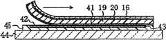
首先,如图4所示,准备例如尺寸为320×420mm左右并且厚度为0.1mm左右的塑料基板19。然后,在塑料基板的两面,通过溅射法等分别形成SiNx膜20、41。SiNx膜20、41的厚度为例如
此时成膜的SiNx膜20具有作为水分低透过性的透明绝缘膜的底涂层的功能。SiNx膜41不仅与SiNx膜20同样具有底涂层的功能,并且发挥如后所述作为弱粘合无机膜的上层膜(第一无机膜)的功能。The
然后,在SiNx膜41上,在从其周端空出10mm以下的宽度的内侧,通过CVD法等形成非晶硅膜42。非晶硅膜42的厚度例如为
接着,在非晶硅膜42上,通过溅射法等形成作为透明薄膜的ITO(氧化铟锡)膜43。ITO膜43的厚度例如为
此处,本发明者对分别成膜于塑料基板19的无机膜彼此的粘合性进行了研究,得到表1所示的结果。Here, the present inventors studied the adhesiveness of the inorganic films formed on the
[表1][Table 1]

已知:由于非晶硅膜42具有较强的膜应力,与无机膜的粘合力较小,如果膜厚为


接着,如图5的塑料基板19的剖视图(图5的上侧图)所示,准备玻璃基板44(支撑基板)。然后,通过利用粘合剂45从SiNx膜41和非晶硅膜42一侧将塑料基板19贴合在玻璃基板44上,使玻璃基板44支撑塑料基板19。此时,粘合剂45覆盖在SiNx膜41表面距离其周端10mm以下宽度的露出部上、和层叠于非晶硅膜42上的ITO膜43上。此外,粘合剂45使用例如在使用250℃以上的加热和药液的湿式工序中也能够获得充分的粘合强度的廉价的材料,使塑料基板19强力地粘合到玻璃基板44上。作为粘合剂,能够使用例如环氧类、硅类、氰丙烯酸酯(cyanoacrylate)类等树脂粘合剂等。Next, as shown in the sectional view of the
其中,本实施方式中,利用粘合剂45将塑料基板19贴合于玻璃基板44,但塑料基板19与玻璃基板44的粘合方法不限于此。例如,还可以将塑料基板19或玻璃基板44的表面通过等离子处理粗糙化后,将其整面向对方侧基板按压而粘合。In this embodiment, the
像这样,如图5的塑料基板19的俯视图(图5的下侧图)所示,在塑料基板19与玻璃基板44之间,在SiNx膜41表面,具有与距离其周端10mm以下宽度的露出部对应的强粘合区域60、和与以被包围在其内侧的方式设置的SiNx膜41与非晶硅膜42的界面区域对应的弱粘合区域61。In this way, as shown in the top view of the
该塑料基板19与玻璃基板44的粘合力比作为弱粘合无机膜的上层膜的SiNx膜41与作为弱粘合无机膜的下层膜的非晶硅膜42的粘合力强。The adhesive force between the
然后,如图6所示,在被玻璃基板44支撑的塑料基板19上,通过溅射法使Ti以例如200nm左右的厚度成膜后,通过光刻法图案化而形成栅极电极21。然后,通过CVD法使SiN膜(400nm)/a-Si(150nm)/n+Si(50nm)作为栅极绝缘膜22/半导体层23/n+半导体层24在250℃的高温下连续成膜,接着通过光刻法使a-Si和n+Si图案化。其后,通过溅射法使Ti以200nm左右的厚度成膜后,通过光刻法图案化而形成源极电极25和漏极电极26。接着,通过干刻法除去TFT16的沟道部的n+Si,在塑料基板19上制造TFT16。塑料基板19与玻璃基板44粘合,因此这样用于形成薄膜的装置能够用与在玻璃基板中使用的装置相同的装置进行处理。Then, as shown in FIG. 6 , on the
其后,如图7所示,通过将作为弱粘合无机膜的上层膜的SiNx膜41与作为弱粘合无机膜的下层膜的非晶硅膜42分离,将形成有TFT16等的塑料基板19从玻璃基板44分离。Thereafter, as shown in FIG. 7, by separating the
此时,在SiNx膜41表面,距离其周端10mm以下宽度的露出部,利用粘合剂45牢固地粘合在玻璃基板44。因此,在该露出部用较强的力分离,在其以外的部分,只要用较弱的力将作为弱粘合无机膜的上层膜的SiNx膜41与作为弱粘合无机膜的下层膜的非晶硅膜42分离即可。从而,能够良好地抑制对塑料基板19和薄膜层叠器件的破坏,能够易于将塑料基板19从玻璃基板44分离。接着,对分离后的塑料基板19施加规定的处理,制作有源矩阵基板13。At this time, on the surface of the
另外,当使用激光照射进行塑料基板19的分离时,能够更容易进行塑料基板19的分离。即,如图8所示,通过激光50的照射等,沿着塑料基板19和SiNx膜41的与非晶硅膜42的周端对应的部位或者比该部位靠内侧的部位,形成在该塑料基板19和SiNx膜41的厚度方向上延伸的截断面51。接着,通过将比截断面51靠内侧的塑料基板19和SiNx膜41从非晶硅膜42分离,将塑料基板19从玻璃基板44分离。In addition, when the separation of the
像这样,如果在分离前形成截断面51,则不需要将比截断面51靠外侧的利用粘合剂45牢固地粘合的部分分离。因此,能够更加易于将塑料基板19从玻璃基板44分离。In this way, if the
(对置基板形成工序)(Counter substrate formation process)
接着,对对置基板形成工序进行说明。首先,与有源矩阵基板形成工序相同,准备塑料基板32,在一个表面上形成弱粘合无机膜的上层膜和弱粘合无机膜的下层膜。此时,弱粘合无机膜的下层膜在弱粘合无机膜的上层膜上,在从其周端空出例如10mm以下宽度的内侧成膜。Next, the counter substrate forming step will be described. First, in the same manner as the active matrix substrate forming process, a plastic substrate 32 is prepared, and an upper layer film of a weakly adhesive inorganic film and a lower layer film of a weakly adhesive inorganic film are formed on one surface. At this time, the lower layer film of the weakly adhesive inorganic film is formed on the upper layer film of the weakly adhesive inorganic film on the inner side with a width of, for example, 10 mm or less from the peripheral end thereof.
进一步,在弱粘合无机膜的下层膜上形成ITO膜等透明无机膜,使用粘合力较强的粘合剂使塑料基板32从ITO膜等透明无机膜一侧与作为支撑基板的玻璃基板粘合。Further, a transparent inorganic film such as an ITO film is formed on the underlayer film of the weakly bonded inorganic film, and an adhesive with strong adhesion is used to connect the plastic substrate 32 from the transparent inorganic film such as the ITO film side to the glass substrate as a supporting substrate. bonding.
接着,在被玻璃基板支撑的塑料基板32上形成彩色滤光片层30和相对电极31等薄膜后,将对置基板14从玻璃基板分离。在该情况下,与有源矩阵基板形成工序相同,在弱粘合无机膜的上层膜表面的距离其周端10mm以下宽度的露出部利用粘合剂牢固地粘合在玻璃基板。因此,在该露出部用较强的力分离,在其以外的部分,只要用较弱的力将弱粘合无机膜的上层膜与弱粘合无机膜的下层膜分离即可。从而,能够良好地抑制对塑料基板32和薄膜层叠器件的破坏,能够易于将塑料基板32从玻璃基板分离。接着,对分离后的塑料基板32施加规定的处理,制造对置基板14。Next, after forming thin films such as the color filter layer 30 and the counter electrode 31 on the plastic substrate 32 supported by the glass substrate, the counter substrate 14 is separated from the glass substrate. In this case, as in the step of forming the active matrix substrate, the exposed portion of the upper film surface of the weakly adhesive inorganic film having a width of 10 mm or less from the peripheral end is firmly bonded to the glass substrate with an adhesive. Therefore, strong force is used to separate the exposed portion, and the upper layer film of the weakly adhesive inorganic film and the lower layer film of the weakly adhesive inorganic film may be separated by relatively weak force in other portions. Therefore, damage to the plastic substrate 32 and the thin-film laminated device can be favorably suppressed, and the plastic substrate 32 can be easily separated from the glass substrate. Next, predetermined processing is applied to the separated plastic substrate 32 to manufacture the counter substrate 14 .
另外,塑料基板32的分离,也可以与有源矩阵基板形成工序相同,通过激光照射等预先在塑料基板32等形成截断面,然后将塑料基板32从玻璃基板分离。In addition, the separation of the plastic substrate 32 may be performed in the same manner as in the active matrix substrate formation process. A cut surface may be formed on the plastic substrate 32 or the like by laser irradiation or the like, and then the plastic substrate 32 may be separated from the glass substrate.
(基板贴合工序)(Board bonding process)
接着,将上述制作的有源矩阵基板13与对置基板14贴合。首先,使密封材料29在有源矩阵基板13或者对置基板14的取向膜17、27一侧的边框区域形成为大致框状。此时,以形成有用于在将有源矩阵基板13与对置基板14贴合时注入液晶材料的注入口的方式形成密封材料29。然后,使有源矩阵基板13与对置基板14以分别设置有取向膜17、27的面相对的方式隔着密封材料29贴合,从注入口注入液晶材料后,将注入口密封,由此形成液晶层15。Next, the
接着,在有源矩阵基板13和对置基板14的与液晶层15一侧相反一侧的面上分别贴合偏光板18、28从而制作液晶显示面板11,在其上设置背光源12完成液晶显示装置10。Next,
另外,在上述实施方式中,支撑基板为玻璃基板44,但本发明不限于此,还可以为金属基板、陶瓷基板、树脂基板等。In addition, in the above-mentioned embodiment, the supporting substrate is the
此外,液晶显示装置10的有源矩阵基板13和对置基板14均由塑料基板19、32构成,但本发明不限于此,只要使有源矩阵基板13和对置基板14的至少一方由塑料基板构成即可。In addition, the
进而,栅极电极21、源极电极25和漏极电极26由Ti形成,但本发明不限于此,还可以由例如Al、Mo、MoW、MoNb、Al合金、Ta或者ITO等形成。Furthermore, the
进而,塑料基板19的截断面51通过照射激光50形成,但不限于此,还可以使用例如划片装置等形成。Furthermore, the
此外,在本实施方式中作为显示装置举例表示了液晶显示装置,但不限于此,还可以为例如场致发光显示装置、等离子体显示装置、电致变色显示装置和场致发射显示器等。In addition, in this embodiment, a liquid crystal display device is shown as an example of the display device, but not limited thereto, for example, an electroluminescent display device, a plasma display device, an electrochromic display device, a field emission display, etc. may be used.
进而,作为弱粘合无机膜的上层膜使用SiNx膜41,但只要能够发挥作为底涂层和弱粘合无机膜的上层膜的功能即可。Furthermore, although the
此外,作为弱粘合无机膜的下层膜使用非晶硅膜42,但只要是与弱粘合无机膜的上层膜的粘合力比粘合剂45小的无机膜即可。In addition, the
(作用效果)(Effect)
接着,对本发明的实施方式的作用效果进行说明。Next, operations and effects of the embodiments of the present invention will be described.
本实施方式的薄膜层叠器件的制造方法,包括利用粘合剂45从作为弱粘合无机膜的上层膜的SiNx膜41和作为弱粘合无机膜的下层膜的非晶硅膜42一侧将塑料基板19贴合到玻璃基板44,使玻璃基板44以比SiNx膜41与非晶硅膜42之间的粘合力强的粘合力支撑塑料基板19的步骤。此外,包括在被玻璃基板44支撑的塑料基板19上层叠多层薄膜的步骤。进而,包括通过分离SiNx膜41与非晶硅膜42,将层叠有多层薄膜的塑料基板19从玻璃基板44分离的步骤。The method of manufacturing a thin film laminated device according to this embodiment includes
根据上述结构,能够使用粘合力强力的粘合剂45使玻璃基板44牢固地支撑容易产生弯曲和挠曲的塑料基板19的状态下,形成多层薄膜。因此,即使在反复进行高温加热和湿式处理等工序的薄膜层叠器件制造中,也能够良好地进行制造处理而使塑料基板19不会从玻璃基板44剥离。According to the above configuration, a multilayer film can be formed in a state where the
此外,在塑料基板19上形成多层薄膜后,不是从强力地粘合的玻璃基板44直接分离,而是通过分离以较弱的粘合力粘合的SiNx膜41与非晶硅膜42,将塑料基板19从玻璃基板44分离。因此,不需要粘合性能会因紫外线照射和加热等而降低这样的高价的粘合材料,此外,不需要紫外线照射和加热所需的处理装置。从而,能够以良好的处理效率和处理成本进行塑料基板19从玻璃基板44的分离。In addition, after forming a multilayer thin film on the
此处,以往的基板剥离的主要原因在于,塑料基板和粘合材料(有机材料)的由热和水分吸收导致的基板膨胀与作为无机材料的玻璃基板等支撑基板相比非常大,因其差而在二者的界面发生应力而产生。与此相对,在本实施方式中,作为无机材料的玻璃基板44与作为进行粘合的有机材料的粘合剂45的界面通过牢固的粘合力粘合,用于在之后的工序中分离基板的弱粘合的界面,由呈现大致相同的热膨胀系数和水分吸收性的无机膜(SiNx膜41和非晶硅膜42)构成。因此,能够抑制在二者的界面产生应力,良好地抑制热和湿式处理工序导致的基板剥离。Here, the main cause of the conventional substrate peeling is that the expansion of the substrate due to the heat and moisture absorption of the plastic substrate and the adhesive material (organic material) is very large compared with the support substrate such as the glass substrate which is an inorganic material. The stress occurs at the interface between the two. On the other hand, in this embodiment, the interface between the
进而,不需要粘合性能因紫外线照射和加热等而降低的高价的粘合材料,能够将需要接近250℃的高温工艺的高性能的TFT16在塑料基板19上通过与玻璃基板的处理相同的工艺简易地制作。Furthermore, there is no need for an expensive adhesive material whose adhesive performance is reduced by ultraviolet irradiation, heating, etc., and the high-
此外,本实施方式中,作为弱粘合无机膜的上层膜,形成作为透明绝缘膜的SiNx膜41。In addition, in the present embodiment, the
根据上述结构,能够将弱粘合无机膜的上层膜作为塑料基板19的底涂层使用。According to the above configuration, the upper layer film of the weakly adhesive inorganic film can be used as an undercoat layer of the
进而,本实施方式中,作为弱粘合无机膜的下层膜,形成非晶硅膜42。Furthermore, in the present embodiment, an
根据上述结构,能够对于粘合剂45,更容易地形成低粘合力的剥离面(非晶硅膜42与其他无机膜的界面)。According to the above configuration, it is possible to more easily form a release surface (interface between the
此外,本实施方式中,非晶硅膜42的厚度为
根据上述结构,如表1所示,由于能够使弱粘合无机膜更加薄膜化,从基板背面一侧的视认性变得良好。从而,例如被两块基板夹住的液晶显示装置和有机EL显示装置的制造处理的自由度变得良好,制造效率变得良好。According to the above configuration, as shown in Table 1, since the weakly adhesive inorganic film can be further thinned, the visibility from the back side of the substrate becomes better. Therefore, for example, a liquid crystal display device and an organic EL display device sandwiched between two substrates have a high degree of freedom in the manufacturing process, and the manufacturing efficiency becomes good.
进而,本实施方式中,在非晶硅膜42上层叠ITO膜43。Furthermore, in the present embodiment, an
根据上述结构,能够保持弱粘合性地使非晶硅膜42良好地变薄至
此外,本实施方式中,在距离SiNx膜41的周端规定宽度的内侧层叠非晶硅膜42。In addition, in the present embodiment, the
根据上述结构,由于在弱粘合无机膜的上层膜即SiNx膜41的周端,SiNx膜41与玻璃基板44利用粘合剂45直接牢固地粘合,在塑料基板上形成薄膜器件之际,对于来自横向的物理的力具有良好的耐性。此外,能够使水和药液等较强地接触从而加速处理时间。According to the above structure, since the
进而,本实施方式中,距离SiNx膜41的周端的上述规定宽度为10mm以下。Furthermore, in the present embodiment, the predetermined width from the peripheral end of the
根据上述结构,能够使塑料基板19牢固地贴合在玻璃基板44的区域为最小限度,使在塑料基板19上制作薄膜层叠器件的区域较广。According to the above configuration, the area where the
此外,在本实施方式中,通过激光50的照射等,沿着塑料基板19和SiNx膜41的与非晶硅膜42的周端对应的部位或者比该部位靠内侧的部位形成截断面51,通过将比截断面51靠内侧的塑料基板19和SiNx膜41从非晶硅膜42分离,由此将塑料基板19从玻璃基板44分离。In addition, in this embodiment, by irradiation of the
根据上述结构,不需要将比塑料基板19的截断面51靠外侧的利用粘合剂45牢固地粘合的部分从玻璃基板44分离。因此,能够更加容易地将塑料基板19从玻璃基板44分离。According to the above configuration, it is not necessary to separate the portion firmly bonded by the adhesive 45 on the outer side of the
产业上的利用可能性Industrial Utilization Possibility
如上所述,本发明对于薄膜层叠器件的制造方法和显示装置的制造方法以及薄膜层叠器件有用。As described above, the present invention is useful for a method of manufacturing a thin film laminated device, a method of manufacturing a display device, and a thin film laminated device.
Claims (11)

Applications Claiming Priority (3)
| Application Number | Priority Date | Filing Date | Title |
|---|---|---|---|
| JP2008-047558 | 2008-02-28 | ||
| JP2008047558 | 2008-02-28 | ||
| PCT/JP2008/002660WO2009107171A1 (en) | 2008-02-28 | 2008-09-25 | Method for manufacturing thin film multilayer device, method for manufacturing display device, and thin film multilayer device |
Publications (2)
| Publication Number | Publication Date |
|---|---|
| CN101903974Atrue CN101903974A (en) | 2010-12-01 |
| CN101903974B CN101903974B (en) | 2012-07-25 |
Family
ID=41015585
Family Applications (1)
| Application Number | Title | Priority Date | Filing Date |
|---|---|---|---|
| CN2008801214975AExpired - Fee RelatedCN101903974B (en) | 2008-02-28 | 2008-09-25 | Method for manufacturing thin film multilayer device, method for manufacturing display device |
Country Status (3)
| Country | Link |
|---|---|
| US (1) | US8236125B2 (en) |
| CN (1) | CN101903974B (en) |
| WO (1) | WO2009107171A1 (en) |
Cited By (3)
| Publication number | Priority date | Publication date | Assignee | Title |
|---|---|---|---|---|
| CN102629593A (en)* | 2011-11-09 | 2012-08-08 | 友达光电股份有限公司 | Flexible electronic device and manufacturing method thereof |
| WO2015172396A1 (en)* | 2014-05-15 | 2015-11-19 | 深圳市华星光电技术有限公司 | Manufacturing method for flexible display |
| CN108574055A (en)* | 2017-03-10 | 2018-09-25 | 株式会社日本显示器 | Manufacturing method of display device, flexible film |
Families Citing this family (10)
| Publication number | Priority date | Publication date | Assignee | Title |
|---|---|---|---|---|
| KR101267529B1 (en)* | 2010-10-30 | 2013-05-24 | 엘지디스플레이 주식회사 | Method of fabricating flexible organic electro luminescent device |
| KR102094729B1 (en)* | 2012-09-27 | 2020-03-30 | 닛테츠 케미컬 앤드 머티리얼 가부시키가이샤 | Display device production method |
| KR101978371B1 (en)* | 2012-10-29 | 2019-05-15 | 삼성디스플레이 주식회사 | Manufacturing method of organic light emitting display device |
| JP2014220348A (en)* | 2013-05-08 | 2014-11-20 | 日東電工株式会社 | Method for manufacturing transparent circuit board |
| KR102215812B1 (en) | 2014-01-09 | 2021-02-17 | 삼성디스플레이 주식회사 | Manufacturing method of device substrate and display device manufatured by using the method |
| EP3151604B1 (en)* | 2014-05-29 | 2019-02-27 | Sony Corporation | Device and method |
| CN107003763A (en) | 2014-11-20 | 2017-08-01 | 东友精细化工有限公司 | Membrane contact sensor and its manufacture method |
| KR20160071735A (en)* | 2014-12-12 | 2016-06-22 | 동우 화인켐 주식회사 | Film Touch Sensor and Method for Fabricating the Same |
| CN104658990B (en)* | 2015-03-02 | 2017-05-17 | 京东方科技集团股份有限公司 | Packaging assembly and preparation method thereof |
| CN106298438A (en)* | 2015-05-13 | 2017-01-04 | 苏州美图半导体技术有限公司 | A kind of method utilizing two-sided adhesive films that substrate is processed |
Family Cites Families (30)
| Publication number | Priority date | Publication date | Assignee | Title |
|---|---|---|---|---|
| JP3739424B2 (en)* | 1994-05-31 | 2006-01-25 | 藤森工業株式会社 | LAMINATED SHEET WITH PLASTICS SUBSTRATE, SUBSTRATE TREATMENT METHOD, AND LIQUID CRYSTAL CELL OR DISPLAY DEVICE MANUFACTURING METHOD |
| JPH1126733A (en) | 1997-07-03 | 1999-01-29 | Seiko Epson Corp | Transfer method of thin film device, thin film device, thin film integrated circuit device, active matrix substrate, liquid crystal display device, and electronic equipment |
| US5856858A (en)* | 1997-12-01 | 1999-01-05 | The Regents Of The University Of California | Plastic substrates for active matrix liquid crystal display incapable of withstanding processing temperature of over 200° C and method of fabrication |
| JP2000248243A (en) | 1999-03-03 | 2000-09-12 | Seiko Epson Corp | Method for manufacturing adhesive sheet and liquid crystal panel |
| KR100407413B1 (en)* | 1999-07-19 | 2003-11-28 | 마쯔시다덴기산교 가부시키가이샤 | Reflector, method of fabricating the same, reflective display device comprising reflector, and method of fabricating the same |
| JP2001267578A (en)* | 2000-03-17 | 2001-09-28 | Sony Corp | Thin film semiconductor device and method of manufacturing the same |
| JP4727024B2 (en)* | 2000-07-17 | 2011-07-20 | 株式会社半導体エネルギー研究所 | Method for manufacturing semiconductor device |
| JP2002122802A (en)* | 2000-10-13 | 2002-04-26 | Fuji Photo Film Co Ltd | Inside surface scanning type image recording device |
| JP2002270553A (en)* | 2001-03-13 | 2002-09-20 | Mitsubishi Gas Chem Co Inc | Manufacturing method of electronic components |
| TW558743B (en)* | 2001-08-22 | 2003-10-21 | Semiconductor Energy Lab | Peeling method and method of manufacturing semiconductor device |
| JP2003229548A (en)* | 2001-11-30 | 2003-08-15 | Semiconductor Energy Lab Co Ltd | Vehicle, display device and method for manufacturing semiconductor device |
| TWI264121B (en)* | 2001-11-30 | 2006-10-11 | Semiconductor Energy Lab | A display device, a method of manufacturing a semiconductor device, and a method of manufacturing a display device |
| KR100443831B1 (en)* | 2001-12-20 | 2004-08-09 | 엘지.필립스 엘시디 주식회사 | Method Of Fabricating Liquid Crystal Display Device |
| US7279239B2 (en)* | 2002-08-07 | 2007-10-09 | Kabushiki Kaisha Toyota Chuo Kenkyusho | Laminating product including adhesion layer and laminate product including protective film |
| TWI313062B (en)* | 2002-09-13 | 2009-08-01 | Ind Tech Res Inst | Method for producing active plastic panel displayers |
| JP2004140267A (en)* | 2002-10-18 | 2004-05-13 | Semiconductor Energy Lab Co Ltd | Semiconductor device and manufacturing method thereof |
| JP2004152563A (en)* | 2002-10-30 | 2004-05-27 | Canon Inc | Display device |
| JP2004311955A (en)* | 2003-03-25 | 2004-11-04 | Sony Corp | Method for manufacturing very thin electro-optical display device |
| JP4725046B2 (en)* | 2003-08-20 | 2011-07-13 | 東ソー株式会社 | Plastic substrate for display and display element |
| US7229900B2 (en)* | 2003-10-28 | 2007-06-12 | Semiconductor Energy Laboratory Co., Ltd. | Semiconductor device, method of manufacturing thereof, and method of manufacturing base material |
| GB0327093D0 (en)* | 2003-11-21 | 2003-12-24 | Koninkl Philips Electronics Nv | Active matrix displays and other electronic devices having plastic substrates |
| US7084045B2 (en)* | 2003-12-12 | 2006-08-01 | Seminconductor Energy Laboratory Co., Ltd. | Method for manufacturing semiconductor device |
| US7259106B2 (en)* | 2004-09-10 | 2007-08-21 | Versatilis Llc | Method of making a microelectronic and/or optoelectronic circuitry sheet |
| EP1760776B1 (en)* | 2005-08-31 | 2019-12-25 | Semiconductor Energy Laboratory Co., Ltd. | Manufacturing method for semiconductor device with flexible substrate |
| JP2010006039A (en)* | 2007-09-05 | 2010-01-14 | Fujifilm Corp | Gas barrier film, and method for sealing display element using gas barrier film |
| JP5226348B2 (en)* | 2008-03-13 | 2013-07-03 | オリンパス株式会社 | Solid-state imaging device and manufacturing method thereof |
| KR101458901B1 (en)* | 2008-04-29 | 2014-11-10 | 삼성디스플레이 주식회사 | Manufacturing method of flexible display device |
| US8182633B2 (en)* | 2008-04-29 | 2012-05-22 | Samsung Electronics Co., Ltd. | Method of fabricating a flexible display device |
| KR101308200B1 (en)* | 2008-05-06 | 2013-09-13 | 엘지디스플레이 주식회사 | Flexible organic electro-luminescence display device and manufacturing method thereof |
| JP2010224422A (en)* | 2009-03-25 | 2010-10-07 | Hitachi Displays Ltd | Display device and manufacturing method thereof |
- 2008
- 2008-09-25CNCN2008801214975Apatent/CN101903974B/ennot_activeExpired - Fee Related
- 2008-09-25WOPCT/JP2008/002660patent/WO2009107171A1/enactiveApplication Filing
- 2008-09-25USUS12/808,275patent/US8236125B2/ennot_activeExpired - Fee Related
Cited By (5)
| Publication number | Priority date | Publication date | Assignee | Title |
|---|---|---|---|---|
| CN102629593A (en)* | 2011-11-09 | 2012-08-08 | 友达光电股份有限公司 | Flexible electronic device and manufacturing method thereof |
| CN102629593B (en)* | 2011-11-09 | 2014-04-02 | 友达光电股份有限公司 | Flexible electronic device and manufacturing method thereof |
| WO2015172396A1 (en)* | 2014-05-15 | 2015-11-19 | 深圳市华星光电技术有限公司 | Manufacturing method for flexible display |
| CN108574055A (en)* | 2017-03-10 | 2018-09-25 | 株式会社日本显示器 | Manufacturing method of display device, flexible film |
| CN108574055B (en)* | 2017-03-10 | 2020-05-05 | 株式会社日本显示器 | Manufacturing method of display device, flexible film |
Also Published As
| Publication number | Publication date |
|---|---|
| CN101903974B (en) | 2012-07-25 |
| WO2009107171A1 (en) | 2009-09-03 |
| US8236125B2 (en) | 2012-08-07 |
| US20100291391A1 (en) | 2010-11-18 |
Similar Documents
| Publication | Publication Date | Title |
|---|---|---|
| CN101903974B (en) | Method for manufacturing thin film multilayer device, method for manufacturing display device | |
| US9013650B2 (en) | Peeling method and method for manufacturing display device using the peeling method | |
| WO2009147769A1 (en) | Method for manufacturing display device, and display device | |
| TW201200933A (en) | Method for fabricating display panel | |
| CN101504947A (en) | Semiconductor device, electro-optical device, electronic apparatus, method for manufacturing semiconductor device, method for manufacturing electro-optical device, and method for manufacturing electro | |
| JP4801579B2 (en) | Method for manufacturing light emitting device | |
| WO2010097855A1 (en) | Method for manufacturing display panel | |
| JP2002072905A (en) | Method for manufacturing thin film laminated device and method for manufacturing liquid crystal display element | |
| US20110043720A1 (en) | Method for manufacturing display device and display device | |
| KR102511463B1 (en) | Thin film transistor array for display device and method for fabricating the same | |
| WO2011155174A1 (en) | Thin film transistor substrate and production method for same | |
| JP2004349520A (en) | Method for transferring thin film device onto plastic substrate and flexible liquid crystal display apparatus | |
| KR20160090959A (en) | Manufacturing method of display device |
Legal Events
| Date | Code | Title | Description |
|---|---|---|---|
| C06 | Publication | ||
| PB01 | Publication | ||
| C10 | Entry into substantive examination | ||
| SE01 | Entry into force of request for substantive examination | ||
| C14 | Grant of patent or utility model | ||
| GR01 | Patent grant | ||
| CF01 | Termination of patent right due to non-payment of annual fee | Granted publication date:20120725 Termination date:20150925 | |
| EXPY | Termination of patent right or utility model |