CN101901834B - Field effect transistor and method for manufacturing the same - Google Patents
Field effect transistor and method for manufacturing the sameDownload PDFInfo
- Publication number
- CN101901834B CN101901834BCN201010194163XACN201010194163ACN101901834BCN 101901834 BCN101901834 BCN 101901834BCN 201010194163X ACN201010194163X ACN 201010194163XACN 201010194163 ACN201010194163 ACN 201010194163ACN 101901834 BCN101901834 BCN 101901834B
- Authority
- CN
- China
- Prior art keywords
- compound semiconductor
- semiconductor layer
- nitride
- defective
- layer
- Prior art date
- Legal status (The legal status is an assumption and is not a legal conclusion. Google has not performed a legal analysis and makes no representation as to the accuracy of the status listed.)
- Expired - Fee Related
Links
Images


Classifications
- H—ELECTRICITY
- H10—SEMICONDUCTOR DEVICES; ELECTRIC SOLID-STATE DEVICES NOT OTHERWISE PROVIDED FOR
- H10D—INORGANIC ELECTRIC SEMICONDUCTOR DEVICES
- H10D30/00—Field-effect transistors [FET]
- H10D30/40—FETs having zero-dimensional [0D], one-dimensional [1D] or two-dimensional [2D] charge carrier gas channels
- H10D30/47—FETs having zero-dimensional [0D], one-dimensional [1D] or two-dimensional [2D] charge carrier gas channels having 2D charge carrier gas channels, e.g. nanoribbon FETs or high electron mobility transistors [HEMT]
- H10D30/471—High electron mobility transistors [HEMT] or high hole mobility transistors [HHMT]
- H10D30/475—High electron mobility transistors [HEMT] or high hole mobility transistors [HHMT] having wider bandgap layer formed on top of lower bandgap active layer, e.g. undoped barrier HEMTs such as i-AlGaN/GaN HEMTs
- H—ELECTRICITY
- H10—SEMICONDUCTOR DEVICES; ELECTRIC SOLID-STATE DEVICES NOT OTHERWISE PROVIDED FOR
- H10D—INORGANIC ELECTRIC SEMICONDUCTOR DEVICES
- H10D30/00—Field-effect transistors [FET]
- H10D30/01—Manufacture or treatment
- H10D30/015—Manufacture or treatment of FETs having heterojunction interface channels or heterojunction gate electrodes, e.g. HEMT
- H—ELECTRICITY
- H10—SEMICONDUCTOR DEVICES; ELECTRIC SOLID-STATE DEVICES NOT OTHERWISE PROVIDED FOR
- H10D—INORGANIC ELECTRIC SEMICONDUCTOR DEVICES
- H10D62/00—Semiconductor bodies, or regions thereof, of devices having potential barriers
- H10D62/80—Semiconductor bodies, or regions thereof, of devices having potential barriers characterised by the materials
- H10D62/85—Semiconductor bodies, or regions thereof, of devices having potential barriers characterised by the materials being Group III-V materials, e.g. GaAs
- H10D62/8503—Nitride Group III-V materials, e.g. AlN or GaN
Landscapes
- Junction Field-Effect Transistors (AREA)
- Thin Film Transistor (AREA)
- Insulated Gate Type Field-Effect Transistor (AREA)
Abstract
Description
Translated fromChinese技术领域technical field
本发明涉及一种由氮化物类Ⅲ-Ⅴ族化合物半导体制造的场效应晶体管,特别涉及常闭型场效应晶体管及其制造方法。The invention relates to a field effect transistor manufactured by nitride-based III-V group compound semiconductors, in particular to a normally closed field effect transistor and a manufacturing method thereof.
背景技术Background technique
目前,作为使用氮化物类Ⅲ-Ⅴ族化合物半导体的AlGaN-GaN异质结构(ヘテロ構造)的场效应晶体管(HFET),将采用纤锌矿结构(ウルツ鉱構造)的氮化物类Ⅲ-Ⅴ族化合物半导体的C面(与表示晶体纵向的C轴垂直的平坦的面)设计成与基板表面平行。因此,在AlGaN-GaN界面通过压电效应、自发极化诱导电子而形成二维电子气(2DEG)。其结果,在上述晶体管中,即使栅极电压为零,当在源极-漏极之间施加电压时,也会使漏极电流流通,因此,将该晶体管称为常开型晶体管。At present, as a field effect transistor (HFET) using an AlGaN-GaN heterostructure (ヘテロ structure) of a nitride-based III-V compound semiconductor, a wurtzite-structure (ウルツ鉱 structure) nitride-based III-V The C-plane (flat plane perpendicular to the C-axis indicating the crystal longitudinal direction) of the group compound semiconductor is designed to be parallel to the substrate surface. Therefore, two-dimensional electron gas (2DEG) is formed at the AlGaN-GaN interface through the piezoelectric effect and spontaneous polarization to induce electrons. As a result, in the above-mentioned transistor, even if the gate voltage is zero, a drain current flows when a voltage is applied between the source and the drain. Therefore, this transistor is called a normally-on transistor.
但是,考虑到在一般电路中的应用时,更希望使用栅极电压为零的情况下不会流通漏极电流的常闭型晶体管,因此,尝试了用于实现常闭化的几种方法。However, in consideration of application to general circuits, it is more desirable to use a normally-off transistor in which a drain current does not flow when the gate voltage is zero, and therefore several methods for realizing normally-off have been tried.
即,在专利文献1(日本特开2000-277724号公报)中,公开了通过采用干式蚀刻减薄栅极电极下方的AlGaN层的厚度来调整2DEG量以谋求实现常闭化的技术。That is, Patent Document 1 (Japanese Patent Application Laid-Open No. 2000-277724 ) discloses a technology for achieving normally-off by adjusting the amount of 2DEG by reducing the thickness of the AlGaN layer below the gate electrode by dry etching.
另外,在非专利文献1(电子情报通信学会技术研究报告ED2005-205、MW2005-159、pp.35~39(2006-1))中,公开了通过利用不产生压电效应、自发极化的纤锌矿结构的无极性面来谋求实现常闭化的技术。In addition, in Non-Patent Document 1 (Technical Research Report ED2005-205, MW2005-159, pp.35-39 (2006-1) of the Society of Electronics, Information and Communications Technology), it is disclosed that by utilizing A technology that realizes normally closed technology by using the non-polar surface of the wurtzite structure.
另外,在非专利文献2(phys.stat,sol.(a)Vol.204、No.6、pp.2064~2067(2007))中,公开了通过使用与Si的MOS晶体管相同的、未采用AlGaN-GaN异质结构的MIS(Metal Insulator Semiconductor:金属绝缘体半导体)结构晶体管来谋求实现常闭化的技术。In addition, in Non-Patent Document 2 (phys.stat, sol.(a) Vol.204, No.6, pp.2064-2067 (2007)), it is disclosed that by using the same MOS transistor as Si, which does not adopt AlGaN-GaN heterostructure MIS (Metal Insulator Semiconductor: Metal Insulator Semiconductor) structure transistors to seek technology to achieve normally-off.
但是,在实现常闭化时成为问题的是如何解决以下(1)和(2)两点。However, how to solve the following two points (1) and (2) becomes a problem when realizing normally closed.
(1)避免导通电阻的增大;(1) Avoid an increase in on-resistance;
(2)维持高沟道迁移率。(2) Maintain high channel mobility.
对此,在专利文献1的技术中,由于在源极-漏极区域存在2DEG,因此能够避免在接触区域中导通电阻增大,但是,由于在沟道区域中2DEG减少,并且通过干式蚀刻进行薄层化造成的损伤导致使沟道迁移率下降,因此产生导通电阻的增大。In contrast, in the technology of
另外,如非专利文献1的技术那样,当采用纤锌矿结构的无极性面(例如a面或m面)时,与利用AlGaAs-GaAs结构时同样,为了生成载流子,必须对AlGaN层进行掺杂。此时,为了降低源极、漏极的接触电阻,不得不增加AlGaN层的掺杂浓度,但是,如果过度增加掺杂浓度,则导致栅极漏电流增大。In addition, as in the technique of Non-Patent
另外,在非专利文献2的技术中,与形成2DEG的情况相比,由于沟道迁移率低,因此,存在无论怎样都不能降低导通电阻的问题。In addition, in the technique of Non-Patent
由此可知,在具有低接触电阻且维持高沟道迁移率的状态下实现常闭型晶体管是多么困难。This shows how difficult it is to realize a normally-off transistor with low contact resistance while maintaining high channel mobility.
发明内容Contents of the invention
本发明的课题在于提供一种具有低接触电阻且能够避免导通电阻的增大、维持高沟道迁移率的实现常闭动作的场效应晶体管及其制造方法。An object of the present invention is to provide a normally-off field effect transistor which has low contact resistance, avoids an increase in on-resistance, and maintains high channel mobility, and a method for manufacturing the same.
为了解决上述课题,本发明的场效应晶体管,其特征在于,具有:In order to solve the above-mentioned problems, the field effect transistor of the present invention is characterized in that, has:
基板,其具有在表面的预先规定的部位形成的表面加工部;A substrate having a surface processed portion formed at a predetermined position on the surface;
缓冲层,其形成在所述基板上;a buffer layer formed on the substrate;
第一氮化物类Ⅲ-Ⅴ族化合物半导体层,其形成在所述缓冲层上,并且具有在对应于所述表面加工部的部位生成的位错,但不具有以所述位错为核的V形的非生长区域即V缺陷;a first nitride-based group III-V compound semiconductor layer formed on the buffer layer and having a dislocation generated at a portion corresponding to the surface processed portion, but having no dislocation having the dislocation as a nucleus The V-shaped non-growth region is the V defect;
第二氮化物类Ⅲ-Ⅴ族化合物半导体层,其形成在所述第一氮化物类Ⅲ-Ⅴ族化合物半导体层上,并且具有以所述位错为核的V形的非生长区域即V缺陷;The second nitride-based III-V group compound semiconductor layer is formed on the first nitride-based III-V group compound semiconductor layer, and has a V-shaped non-growth region with the dislocation as a nucleus, that is, V defect;
第三氮化物类Ⅲ-Ⅴ族化合物半导体层,其以不填埋所述V缺陷的方式形成在所述第二氮化物类Ⅲ-Ⅴ族化合物半导体层上,并且具有与所述V缺陷相连接的非生长区域,但不具有与所述V缺陷不同的新的V缺陷;The third nitride-based III-V group compound semiconductor layer is formed on the second nitride-based III-V group compound semiconductor layer in such a manner that the V defect is not buried, and has a phase similar to the V defect connected non-growth regions, but without new V-defects different from said V-defects;
第四氮化物类Ⅲ-Ⅴ族化合物半导体层,其形成在所述第三氮化物类Ⅲ-Ⅴ族化合物半导体层上,具有薄层部和平坦部,该薄层部沿着所述V缺陷及与所述V缺陷相连接的非生长区域形成,该平坦部与所述薄层部相连接并在所述V缺陷之外形成,厚度比所述薄层部厚;A fourth nitride-based III-V group compound semiconductor layer formed on the third nitride-based III-V group compound semiconductor layer, having a thin portion and a flat portion, the thin portion along the V defect and a non-growth region connected to the V-defect is formed, the flat part is connected to the thin-layer part and formed outside the V-defect, and has a thickness thicker than that of the thin-layer part;
由所述第一至第三氮化物类Ⅲ-Ⅴ族化合物半导体层构成沟道层,由所述第四氮化物类Ⅲ-Ⅴ族化合物半导体层构成势垒层,由所述第三氮化物类Ⅲ-Ⅴ族化合物半导体层和所述第四氮化物类Ⅲ-Ⅴ族化合物半导体层构成异质结。A channel layer is formed by the first to third nitride-based III-V compound semiconductor layers, a barrier layer is formed by the fourth nitride-based III-V compound semiconductor layer, and a barrier layer is formed by the third nitride-based The III-V group-like compound semiconductor layer and the fourth nitride-like III-V group compound semiconductor layer form a heterojunction.
根据该发明的场效应晶体管,在由所述沟道层和势垒层构成的异质结界面附近的、构成所述沟道层一部分的第三氮化物类Ⅲ-Ⅴ族化合物半导体层中,在面对所述势垒层的平坦部的区域,形成与所述平坦部的厚度与组成相对应的二维电子气。另一方面,在构成所述沟道层一部分的第二、第三氮化物类Ⅲ-Ⅴ族化合物半导体层中、面对所述势垒层的薄层部的区域,几乎不形成二维电子气。因此,通过在所述势垒层中的所述薄层部上形成栅极电极,可以实现进行常闭动作的场效应晶体管。According to the field effect transistor of the present invention, in the third nitride-based group III-V compound semiconductor layer constituting a part of the channel layer near the heterojunction interface formed by the channel layer and the barrier layer, In a region facing the flat portion of the barrier layer, a two-dimensional electron gas corresponding to the thickness and composition of the flat portion is formed. On the other hand, in the second and third nitride-based III-V group compound semiconductor layers constituting a part of the channel layer, in the region facing the thin layer portion of the barrier layer, almost no two-dimensional electrons are formed. gas. Therefore, by forming a gate electrode on the thin portion of the barrier layer, a field effect transistor that operates normally off can be realized.
另外,由于所述势垒层的薄层部形成在所述V缺陷及与所述V缺陷相连接的非生长区域上,因此,不进行蚀刻也能够使该薄层部的厚度比平坦部的厚度薄。因此,根据该发明,能够避免导通电阻的增大,而不会由于蚀刻损坏使沟道迁移率下降。作为一个具体例,所述势垒层的薄层部的厚度设定在所述平坦部的厚度的50%以下。In addition, since the thin portion of the barrier layer is formed on the V defect and the non-growth region connected to the V defect, the thin portion can be made thicker than the flat portion without etching. Thin. Therefore, according to this invention, an increase in on-resistance can be avoided without decreasing channel mobility due to etching damage. As a specific example, the thickness of the thin portion of the barrier layer is set to be 50% or less of the thickness of the flat portion.
另外,在一实施方式的场效应晶体管中,所述V缺陷有规则地排列。In addition, in the field effect transistor according to one embodiment, the V defects are regularly arranged.
根据该实施方式,在栅极电极的下方容易集中配置所述V缺陷。According to this embodiment, the V defects are easily arranged concentratedly under the gate electrode.
另外,在一实施方式的场效应晶体管中,具有栅极电极,该栅极电极形成在有规则地排列的所述V缺陷之上。In addition, the field effect transistor according to one embodiment has a gate electrode formed on the regularly arranged V defects.
根据该实施方式,由于栅极电极形成在所述势垒层中的所述V缺陷上的薄层部上,因此能够实现进行常闭动作的场效应晶体管。According to this embodiment, since the gate electrode is formed on the thin layer portion above the V defect in the barrier layer, it is possible to realize a field effect transistor performing a normally-off operation.
另外,在一实施方式的场效应晶体管中,具有绝缘膜,该绝缘膜形成在所述第四氮化物类Ⅲ-Ⅴ族化合物半导体层与栅极电极之间。In addition, the field effect transistor according to one embodiment has an insulating film formed between the fourth nitride-based III-V group compound semiconductor layer and the gate electrode.
根据该实施方式,与未形成绝缘膜的情况相比,由于能够使夹断电压(ピンチオフ)增大,因此适用于电路应用。作为一个具体例,在未形成所述绝缘膜的情况下夹断电压为0V左右,与此相对,能够通过形成所述绝缘膜,使夹断电压保持在+2~+3V左右。According to this embodiment, since the pinch-off voltage can be increased compared with the case where no insulating film is formed, it is suitable for circuit applications. As a specific example, when the insulating film is not formed, the pinch-off voltage is about 0V, but by forming the insulating film, the pinch-off voltage can be maintained at about +2 to +3V.
另外,本发明的场效应晶体管的制造方法,其特征在于,In addition, the method for manufacturing a field effect transistor of the present invention is characterized in that
在基板上使用抗蚀剂或者具有耐蚀性的材料形成掩模图案;Forming a mask pattern on the substrate using a resist or a corrosion-resistant material;
通过对所述基板中未被所述掩模图案覆盖的部分进行蚀刻,在所述基板的预先规定的部分形成凸状的表面加工部;forming a convex surface processing portion on a predetermined portion of the substrate by etching a portion of the substrate not covered by the mask pattern;
接着在所述基板上形成缓冲层;Then forming a buffer layer on the substrate;
在从对应于所述凸状的表面加工部的部位生成位错、但不生成以所述位错为核的V形非生长区域即V缺陷的生长温度条件下,使构成沟道层的第一氮化物类Ⅲ-Ⅴ族化合物半导体层在所述缓冲层上生长;Under the growth temperature condition that dislocations are generated from the portion corresponding to the convex surface processing portion, but the V-shaped non-growth region having the dislocations as nuclei, i.e. V defects, is not generated, the second layer constituting the channel layer is a nitride-type III-V compound semiconductor layer is grown on the buffer layer;
在生成所述V缺陷的生长温度条件下,使构成沟道层的第二氮化物类Ⅲ-Ⅴ族化合物半导体层在所述第一氮化物类Ⅲ-Ⅴ族化合物半导体层上生长;growing the second nitride-based III-V group compound semiconductor layer constituting the channel layer on the first nitride-based III-V group compound semiconductor layer under the growth temperature condition for generating the V defect;
在生成不填埋所述第二氮化物类Ⅲ-Ⅴ族化合物半导体层中生成的V缺陷并且与所述V缺陷相连接的非生长区域、但不生成与所述V缺陷不同的新的V缺陷的生长温度条件下,使构成沟道层的第三氮化物类Ⅲ-Ⅴ族化合物半导体层在所述第二氮化物类Ⅲ-Ⅴ族化合物半导体层上生长;generating a non-growth region that does not fill the V defect generated in the second nitride-based III-V group compound semiconductor layer and is connected to the V defect, but does not generate a new V defect different from the V defect growing the third nitride-based III-V group compound semiconductor layer constituting the channel layer on the second nitride-based III-V group compound semiconductor layer under the growth temperature condition of the defect;
在所述第三氮化物类Ⅲ-Ⅴ族化合物半导体层上形成第四氮化物类Ⅲ-Ⅴ族化合物半导体层,该第四氮化物类Ⅲ-Ⅴ族化合物半导体层构成具有薄层部和平坦部的势垒层,且与所述第三氮化物类Ⅲ-Ⅴ族化合物半导体层构成异质结,该薄层部沿着所述V缺陷及与所述V缺陷相连接的非生长区域形成,该平坦部与所述薄层部相连接并在所述V缺陷之外形成,厚度比所述薄层部厚。A fourth nitride-based III-V compound semiconductor layer is formed on the third nitride-based III-V compound semiconductor layer, and the fourth nitride-based III-V compound semiconductor layer has a thin layer portion and a flat part of the barrier layer, and form a heterojunction with the third nitride-based III-V compound semiconductor layer, the thin layer is formed along the V defect and the non-growth region connected to the V defect , the flat portion is connected to the thin layer portion and formed outside the V defect, and has a thickness greater than that of the thin layer portion.
根据本发明的场效应晶体管的制造方法,由利用掩模图案蚀刻所述基板而形成的凸状的表面加工部引起的位错,形成在第一氮化物类Ⅲ-Ⅴ族化合物半导体层中,以所述位错为核的V缺陷形成在第二氮化物类Ⅲ-Ⅴ族化合物半导体层中,与所述V缺陷相连接的非生长区域形成在第三氮化物类Ⅲ-Ⅴ族化合物半导体层中。另外,所述势垒层的薄层部形成在所述V缺陷及与所述V缺陷相连接的非生长区域上,由于不进行蚀刻也能够使该薄层部厚度比平坦部薄,因此不会使沟道迁移率下降。另外,在构成沟道层一部分的第二、第三氮化物类Ⅲ-Ⅴ族化合物半导体层中、面对所述势垒层的薄层部的区域,几乎不形成二维电子气。因此,能够通过在所述势垒层中的所述薄层部上形成栅极电极来维持高沟道迁移率,并且可以实现进行常闭动作的场效应晶体管。According to the method of manufacturing a field effect transistor of the present invention, dislocations caused by the convex surface processing portion formed by etching the substrate using a mask pattern are formed in the first nitride-based III-V compound semiconductor layer, A V defect with the dislocation as a nucleus is formed in the second nitride-based III-V group compound semiconductor layer, and a non-growth region connected to the V defect is formed in the third nitride-based III-V group compound semiconductor layer. layer. In addition, the thin layer portion of the barrier layer is formed on the V defect and the non-growth region connected to the V defect, and since the thickness of the thin layer portion can be made thinner than that of the flat portion without etching, it is not necessary to will reduce the channel mobility. In addition, in the second and third nitride-based III-V group compound semiconductor layers constituting a part of the channel layer, a region facing the thin portion of the barrier layer hardly forms a two-dimensional electron gas. Therefore, high channel mobility can be maintained by forming a gate electrode on the thin portion of the barrier layer, and a field effect transistor performing a normally-off operation can be realized.
另外,在一实施方式的场效应晶体管的制造方法中,对所述基板进行蚀刻的方法为干式蚀刻、湿式蚀刻或者干式蚀刻与湿式蚀刻的组合。In addition, in the method for manufacturing a field effect transistor according to one embodiment, the method of etching the substrate is dry etching, wet etching, or a combination of dry etching and wet etching.
根据该实施方式,根据所述基板的材质的不同,能够在可进行湿式蚀刻的情况下进行湿式蚀刻,在难以进行湿式蚀刻的情况下进行干式蚀刻。另外,也能够将干式蚀刻与湿式蚀刻组合以充分发挥两者的特长。According to this embodiment, depending on the material of the substrate, wet etching can be performed when wet etching is possible, and dry etching can be performed when wet etching is difficult. In addition, it is also possible to combine dry etching and wet etching to fully utilize the advantages of both.
另外,在一实施方式的场效应晶体管的制造方法中,当所述基板由不容易进行湿式蚀刻的材料制成时,利用干式蚀刻对所述基板进行蚀刻。In addition, in the method for manufacturing a field effect transistor according to one embodiment, when the substrate is made of a material that is not readily wet-etched, the substrate is etched by dry etching.
根据该实施方式,当所述基板由使用溶液难以进行湿式蚀刻的蓝宝石、碳化硅(SiC)或GaN等氮化物类Ⅲ-Ⅴ族化合物半导体层制成时,能够通过采用干式蚀刻,容易地蚀刻所述基板。According to this embodiment, when the substrate is made of a nitride-based III-V group compound semiconductor layer such as sapphire, silicon carbide (SiC), or GaN, which is difficult to perform wet etching using a solution, it can be easily etched by dry etching. The substrate is etched.
另外,在一实施方式的场效应晶体管的制造方法中,用于所述干式蚀刻的蚀刻气体为氯类气体。In addition, in the method for manufacturing a field effect transistor according to one embodiment, the etching gas used for the dry etching is a chlorine-based gas.
根据该实施方式,通过利用氯类气体(氯气、氯化硅、氯化硼等)作为干式蚀刻的蚀刻气体,能够对由使用溶液难以进行湿式蚀刻的材料制成的基板有效地进行蚀刻。According to this embodiment, by using chlorine-based gas (chlorine gas, silicon chloride, boron chloride, etc.) as an etching gas for dry etching, it is possible to efficiently etch a substrate made of a material that is difficult to wet-etch using a solution.
另外,本发明的场效应晶体管的制造方法,其特征在于,In addition, the method for manufacturing a field effect transistor of the present invention is characterized in that
在基板上对用于选择生长的掩模材料进行构图,在所述基板上的预先规定的部位利用已构图的所述掩模材料形成表面加工部;patterning a mask material for selective growth on a substrate, and using the patterned mask material to form a surface processing portion at a predetermined position on the substrate;
接着在所述基板上形成缓冲层;Then forming a buffer layer on the substrate;
在从对应于所述表面加工部的部位生成位错、但不生成以所述位错为核的V形非生长区域即V缺陷的生长温度条件下,使构成沟道层的第一氮化物类Ⅲ-Ⅴ族化合物半导体层在所述缓冲层上生长;The first nitride constituting the channel layer is formed under a growth temperature condition in which dislocations are generated from the portion corresponding to the surface processing portion, but V-shaped non-growth regions, that is, V defects, which have the dislocations as nuclei, are not generated. A group III-V compound semiconductor layer is grown on the buffer layer;
在生成所述V缺陷的生长温度条件下,使构成沟道层的第二氮化物类Ⅲ-Ⅴ族化合物半导体层在所述第一氮化物类Ⅲ-Ⅴ族化合物半导体层上生长;growing the second nitride-based III-V group compound semiconductor layer constituting the channel layer on the first nitride-based III-V group compound semiconductor layer under the growth temperature condition for generating the V defect;
在生成不填埋所述第二氮化物类Ⅲ-Ⅴ族化合物半导体层中生成的V缺陷并且与所述V缺陷相连接的非生长区域、但不生成与所述V缺陷不同的新的V缺陷的生长温度条件下,使构成沟道层的第三氮化物类Ⅲ-Ⅴ族化合物半导体层生长在所述第二氮化物类Ⅲ-Ⅴ族化合物半导体层上;generating a non-growth region that does not fill the V defect generated in the second nitride-based III-V group compound semiconductor layer and is connected to the V defect, but does not generate a new V defect different from the V defect growing the third nitride-based III-V group compound semiconductor layer constituting the channel layer on the second nitride-based III-V group compound semiconductor layer under the defect growth temperature condition;
在所述第三氮化物类Ⅲ-Ⅴ族化合物半导体层上形成第四氮化物类Ⅲ-Ⅴ族化合物半导体层,该第四氮化物类Ⅲ-Ⅴ族化合物半导体层构成具有薄层部和平坦部的势垒层,且与所述第三氮化物类Ⅲ-Ⅴ族化合物半导体层构成异质结,该薄层部沿着所述V缺陷及与所述V缺陷相连接的非生长区域形成,该平坦部与所述薄层部相连接并在所述V缺陷之外形成,厚度比所述薄层部厚。A fourth nitride-based III-V compound semiconductor layer is formed on the third nitride-based III-V compound semiconductor layer, and the fourth nitride-based III-V compound semiconductor layer has a thin layer portion and a flat part of the barrier layer, and form a heterojunction with the third nitride-based III-V compound semiconductor layer, the thin layer is formed along the V defect and the non-growth region connected to the V defect , the flat portion is connected to the thin layer portion and formed outside the V defect, and has a thickness greater than that of the thin layer portion.
根据本发明的制造方法,由于在所述基板上通过对掩模材料进行构图来形成表面加工部,因此,无需蚀刻基板也能够维持基板表面的平坦性。即,在对基板表面进行干式蚀刻加工的情况下,不可避免地会在基板的表面产生加工造成的粗糙。另外,根据该实施方式,与通过干式蚀刻加工来形成表面加工部的情况相比,能够对表面加工部更加精细地进行构图。According to the manufacturing method of the present invention, since the surface processed portion is formed by patterning the mask material on the substrate, the flatness of the substrate surface can be maintained without etching the substrate. That is, when dry etching is performed on the surface of the substrate, roughness due to the processing inevitably occurs on the surface of the substrate. In addition, according to this embodiment, the surface-processed portion can be patterned more finely than when the surface-processed portion is formed by dry etching.
另外,在一实施方式的场效应晶体管的制造方法中,所述用于选择生长的掩模材料为氧化硅。In addition, in a method for manufacturing a field effect transistor according to an embodiment, the mask material for selective growth is silicon oxide.
根据该实施方式的制造方法,通过将作为用于选择生长的掩模材料(表面加工部)设为氧化硅(SiO2),由于难以在所述表面加工部上沉积GaN,因此在所述表面加工部上容易进行选择生长。According to the manufacturing method of this embodiment, by setting silicon oxide (SiO2 ) as the mask material (surface processing portion) for selective growth, since it is difficult to deposit GaN on the surface processing portion, the surface It is easy to perform selective growth on the processed part.
另外,在一实施方式的场效应晶体管的制造方法中,所述第一氮化物类Ⅲ-Ⅴ族化合物半导体层的生长温度在1000℃以上。In addition, in the method for manufacturing a field effect transistor according to one embodiment, the growth temperature of the first nitride-based III-V group compound semiconductor layer is 1000° C. or higher.
根据该实施方式的制造方法,能够防止在所述第一氮化物类Ⅲ-Ⅴ族化合物半导体层中形成凹坑。According to the manufacturing method of this embodiment, formation of pits in the first nitride-based Group III-V compound semiconductor layer can be prevented.
另外,在一实施方式的场效应晶体管的制造方法中,所述第二氮化物类Ⅲ-Ⅴ族化合物半导体层的生长温度在700℃以上且900℃以下。In addition, in the method for manufacturing a field effect transistor according to one embodiment, the growth temperature of the second nitride-based III-V group compound semiconductor layer is 700° C. or higher and 900° C. or lower.
根据该实施方式的制造方法,与所述生长温度的下限不足700℃的情况相比,或者与所述生长温度的上限超过900℃的情况相比,能够容易地在所述第二氮化物类Ⅲ-Ⅴ族化合物半导体层中形成V缺陷。According to the manufacturing method of this embodiment, compared with the case where the lower limit of the growth temperature is less than 700°C, or the case where the upper limit of the growth temperature exceeds 900°C, the second nitride-based V defects are formed in the III-V group compound semiconductor layer.
另外,在一实施方式的场效应晶体管的制造方法中,所述第二氮化物类Ⅲ-Ⅴ族化合物半导体层的层厚在100nm以下。In addition, in the method for manufacturing a field effect transistor according to one embodiment, the layer thickness of the second nitride-based III-V group compound semiconductor layer is 100 nm or less.
根据该实施方式的制造方法,通过使所述第二氮化物类Ⅲ-Ⅴ族化合物半导体层的层厚在100nm以下,能够在尽量使结晶性差的区域变薄的基础上可靠地生成V缺陷。即,低温生长的第二氮化物类Ⅲ-Ⅴ族化合物半导体层与其前后制成的层(第一、第三氮化物类Ⅲ-Ⅴ族化合物半导体层)相比,结晶性差。According to the manufacturing method of this embodiment, by setting the layer thickness of the second nitride-based III-V group compound semiconductor layer to 100 nm or less, it is possible to reliably generate V defects while reducing the thickness of the region poor in crystallinity as much as possible. That is, the second nitride-based III-V compound semiconductor layer grown at a low temperature has lower crystallinity than the layers formed before and after it (first and third nitride-based III-V compound semiconductor layers).
另外,在一实施方式的场效应晶体管的制造方法中,在使所述第二氮化物类Ⅲ-Ⅴ族化合物半导体层生长时,作为Ⅲ族的有机金属原料,采用具有乙基的有机金属。In addition, in the method for manufacturing a field effect transistor according to one embodiment, when growing the second nitride-based Group III-V compound semiconductor layer, an organic metal having an ethyl group is used as a Group III organic metal raw material.
根据该实施方式的制造方法,能够避免大量的碳被掺杂在第二氮化物类Ⅲ-Ⅴ族化合物半导体层中这样的不良现象。即,在利用具有乙基的有机金属(三乙基镓(TEG)、三乙基铝(TEA))使第二氮化物类Ⅲ-Ⅴ族化合物半导体层低温生长时,能够避免发生大量的碳被掺杂在第二氮化物类Ⅲ-Ⅴ族化合物半导体层中这样的不良现象。According to the manufacturing method of this embodiment, it is possible to avoid the disadvantage that a large amount of carbon is doped in the second nitride-based III-V group compound semiconductor layer. That is, when the second nitride-based III-V group compound semiconductor layer is grown at low temperature using an organic metal having an ethyl group (triethylgallium (TEG), triethylaluminum (TEA)), a large amount of carbon can be avoided. The undesirable phenomenon of being doped in the second nitride-based III-V compound semiconductor layer.
另外,在一实施方式的场效应晶体管的制造方法中,所述第三氮化物类Ⅲ-Ⅴ族化合物半导体层的生长温度在950℃以上且1100℃以下。In addition, in the method for manufacturing a field effect transistor according to one embodiment, the growth temperature of the third nitride-based III-V group compound semiconductor layer is 950° C. or higher and 1100° C. or lower.
根据该实施方式的制造方法,通过将所述生长温度的下限温度设定在950℃,即使接受产生少量凹坑这一结果,也能够做到在第三氮化物类Ⅲ-Ⅴ族化合物半导体层中不生成新的V缺陷。另外,通过将所述生长温度的上限温度设定在1100℃,能够通过促进横向生长,做到V缺陷不被填埋。According to the manufacturing method of this embodiment, by setting the lower limit temperature of the growth temperature at 950° C., even if the result of a small number of pits is accepted, it is possible to realize the growth rate in the third nitride-based III-V group compound semiconductor layer. No new V defects are generated in . In addition, by setting the upper limit temperature of the growth temperature at 1100° C., it is possible to prevent V defects from being buried by promoting lateral growth.
另外,在氮化物类Ⅲ-Ⅴ族化合物半导体中,以与InGaN相同程度的生长温度使需要1000℃以上生长温度的AlGaN晶体生长的情况下,则以晶体中的贯通位错或者形成在晶体中的层叠位错为核,形成晶体不生长的V形部分即所谓V缺陷。另一方面,已知这样的事实,例如,在被图案化的蓝宝石基板(PSS基板)上生长的GaN中,当通过横向生长在图案上延伸的晶体融合时,在图案的顶点部分形成贯通位错。In addition, in the case of growing an AlGaN crystal requiring a growth temperature of 1000° C. or higher in a nitride-based III-V compound semiconductor at a growth temperature similar to that of InGaN, threading dislocations in the crystal or formed in the crystal The stacking dislocation is the nucleus, forming a V-shaped part where the crystal does not grow, which is the so-called V defect. On the other hand, the fact is known that, for example, in GaN grown on a patterned sapphire substrate (PSS substrate), when crystals extending on the pattern by lateral growth fuse, a through site is formed at the apex portion of the pattern wrong.
通过将上述两个现象组合,能够在任意的位置形成V缺陷。由于该V缺陷对于发光元件产生增大漏电流等恶劣影响,因此有必要极力抑制该V缺陷的产生,但是,在本发明中,通过积极利用在发光元件中被视为问题的V缺陷,有助于实现晶体管的常闭化。By combining the above two phenomena, V defects can be formed at arbitrary positions. Since this V defect has adverse effects such as increased leakage current on the light-emitting element, it is necessary to suppress the occurrence of this V defect as much as possible. However, in the present invention, by actively utilizing the V defect that is regarded as a problem in the light-emitting element, Contributes to the realization of normally closed transistors.
在此,为了不使晶体管特性极度下降,不优选仅将形成V缺陷的第二氮化物类Ⅲ-Ⅴ族化合物半导体层作为沟道层。这是因为在生成V缺陷的温度下生长的氮化物类Ⅲ-Ⅴ族化合物半导体层的结晶性差。Here, it is not preferable to use only the second nitride-based III-V group compound semiconductor layer in which V defects are formed as the channel layer in order not to degrade the transistor characteristics extremely. This is because the crystallinity of the nitride-based group III-V compound semiconductor layer grown at a temperature at which V defects are generated is poor.
于是,使在不生成V缺陷的生长温度下生长的第一氮化物类Ⅲ-Ⅴ族化合物半导体层生长,接着,使生成有V缺陷的第二氮化物类Ⅲ-Ⅴ族化合物半导体层生长一定厚度,然后,使在抑制V缺陷的生长且不填埋形成在第二氮化物类Ⅲ-Ⅴ族化合物半导体层中的V缺陷的生长温度下生长的、构成沟道层的第三氮化物类Ⅲ-Ⅴ族化合物半导体层生长,由此,与在低温下使所有层生长的情况相比,能够实现优异的晶体管特性。Then, the first nitride-based III-V group compound semiconductor layer grown at a growth temperature at which V defects are not formed is grown, and then the second nitride-based III-V group compound semiconductor layer in which V defects are generated is grown by a certain amount. thickness, and then, the third nitride-based channel layer grown at a growth temperature that suppresses the growth of V-defects and does not bury the V-defects formed in the second nitride-based III-V group compound semiconductor layer By growing the III-V group compound semiconductor layers, excellent transistor characteristics can be realized compared to the case where all the layers are grown at a low temperature.
根据本发明的场效应晶体管,由第四氮化物类Ⅲ-Ⅴ族化合物半导体层构成的势垒层的薄层部,形成在第二氮化物类Ⅲ-Ⅴ族化合物半导体层的V缺陷以及与所述V缺陷相连接的第三氮化物类Ⅲ-Ⅴ族化合物半导体层的非生长区域上。因此,根据本发明,不对所述薄层部进行蚀刻也能够使该薄层部的厚度比平坦部薄,能够在栅极电极区域下维持无蚀刻损伤的状态,避免沟道迁移率的下降,避免导通电阻的增大,并且实现进行常闭动作的场效应晶体管。According to the field effect transistor of the present invention, the thin layer portion of the barrier layer composed of the fourth nitride-based III-V group compound semiconductor layer, the V defect and the V defect formed in the second nitride-based III-V group compound semiconductor layer The V defect is connected to the non-growth region of the third nitride-based III-V group compound semiconductor layer. Therefore, according to the present invention, the thickness of the thin layer portion can be made thinner than that of the flat portion without etching the thin layer portion, a state without etching damage can be maintained under the gate electrode region, and a decrease in channel mobility can be avoided. A field effect transistor that performs normally-off operation is realized while avoiding an increase in on-resistance.
附图说明Description of drawings
图1是表示本发明的场效应晶体管的第一实施方式的层结构的立体图;1 is a perspective view showing a layer structure of a first embodiment of a field effect transistor of the present invention;
图2是包括所述第一实施方式的电极的晶体管结构的剖面图;2 is a cross-sectional view of a transistor structure including electrodes of the first embodiment;
图3A是用于说明该第一实施方式的场效应晶体管的制造工序的立体图;3A is a perspective view for explaining the manufacturing process of the field effect transistor of the first embodiment;
图3B是用于说明上述制造工序的立体图;Fig. 3B is a perspective view for explaining the above-mentioned manufacturing process;
图3C是用于说明上述制造工序的立体图;FIG. 3C is a perspective view for explaining the above-mentioned manufacturing process;
图3D是用于说明上述制造工序的立体图;FIG. 3D is a perspective view for explaining the above manufacturing process;
图3E是用于说明上述制造工序的立体图;FIG. 3E is a perspective view for explaining the above manufacturing process;
图3F是用于说明上述制造工序的立体图;FIG. 3F is a perspective view for explaining the above manufacturing process;
图4A是用于说明本发明的场效应晶体管的第二实施方式的制造工序的立体图;4A is a perspective view for explaining the manufacturing process of the second embodiment of the field effect transistor of the present invention;
图4B是用于说明上述制造工序的立体图;Fig. 4B is a perspective view for explaining the above-mentioned manufacturing process;
图4C是用于说明上述制造工序的立体图;FIG. 4C is a perspective view for explaining the above manufacturing process;
图4D是用于说明上述制造工序的立体图;FIG. 4D is a perspective view for explaining the above manufacturing process;
图4E是用于说明上述制造工序的立体图;FIG. 4E is a perspective view for explaining the above manufacturing process;
图4F是用于说明上述制造工序的立体图;FIG. 4F is a perspective view for explaining the above manufacturing process;
图5是包括上述第二实施方式的电极的晶体管结构的剖面图。FIG. 5 is a cross-sectional view of a transistor structure including electrodes of the second embodiment described above.
附图标记说明Explanation of reference signs
1,51蓝宝石基板1,51 sapphire substrate
2,52低温生长GaN缓冲层2,52 low temperature growth of GaN buffer layer
3,53第一GaN层3,53 First GaN layer
4第二GaN层4 Second GaN layer
5第三GaN层5 third GaN layer
6,56 AlGaN势垒层6,56 AlGaN barrier layer
6a,56a薄层部6a, 56a thin section
6b,56b平坦部6b, 56b flat part
7,8,57,58源极-漏极电极7, 8, 57, 58 source-drain electrodes
9,59栅极电极9, 59 grid electrode
10,60沟道层10, 60 channel layer
11凸状的表面加工部11Convex surface processing part
12,63贯通位错12, 63 threading dislocations
13,65V缺陷13, 65V defect
13A壁面13A wall
22,72二维电子气22,72 Two-dimensional electron gas
23延长V缺陷23 Extended V defect
G1,G51非生长区域G1, G51 non-growth regions
61 SiO2膜61SiO2 film
62点状的SiO2膜62-dotSiO2 film
具体实施方式Detailed ways
通过以下的详细说明及附图能够更加充分地理解本发明。附图只是用来进行说明,并不限定本发明。The present invention can be understood more fully by the following detailed description and accompanying drawings. The accompanying drawings are for illustration only and do not limit the invention.
下面,根据图示的实施方式更加详细地说明本发明。Next, the present invention will be described in more detail based on the illustrated embodiments.
(第一实施方式)(first embodiment)
图1是表示本发明的场效应晶体管的第一实施方式的层结构的立体图,图2是包括所述第一实施方式的电极的晶体管结构的剖面图。另外,图3A~图3E及图3F是用于说明该第一实施方式的场效应晶体管的制造工序的立体图和剖面图。FIG. 1 is a perspective view showing a layer structure of a first embodiment of a field effect transistor according to the present invention, and FIG. 2 is a cross-sectional view of a transistor structure including electrodes of the first embodiment. 3A to 3E and 3F are perspective views and cross-sectional views for explaining the manufacturing process of the field effect transistor of the first embodiment.
首先,说明该第一实施方式的场效应晶体管的制造工序。First, the manufacturing process of the field effect transistor of the first embodiment will be described.
首先,在图3A所示的蓝宝石基板1上涂覆抗蚀剂或具有耐蚀性的材料,接着如图3B所示,利用光刻技术,在成为栅极电极下方的区域形成由所述抗蚀剂构成的多个点状的掩模图案10。该多个点状的掩模图案10有规则地排成一列。另外,所述抗蚀剂为AZ类,厚度设定在10μm。First, a resist or a corrosion-resistant material is coated on the
接着,通过使用氯气的ICP-RIE(感应耦合等离子-反应性离子蚀刻),对蓝宝石基板1仅蚀刻1μm。此时,由于蚀刻过程中的热等,点状的掩模图案10逐渐缩小。因此,如图3C所示,通过所述蚀刻,在所述点状的掩模图案10下方的蓝宝石基板1上,形成大致前端尖细的山形的凸状表面加工部11。Next, the
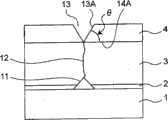
接着,如图3D所示,作为Ga原料气体使用TEG(三乙基镓),在通过表面加工形成有凸状的表面加工部11的蓝宝石基板1上,在基板温度550℃的条件下,使低温生长GaN缓冲层2生长到厚度为50nm。然后,在基板温度1150℃的条件下,使作为第一氮化物类Ⅲ-Ⅴ族化合物半导体层的第一GaN层3生长到厚度为3μm。此时,从与蓝宝石基板1上的GaN缓冲层2相接的底面横向生长的第一GaN层3在凸状的表面加工部11的顶点部分融合时形成贯通位错12。该贯通位错12与形成在所述底面的位错不同,在生长过程中不会消失。另外,该第一GaN层3由于在基板温度1150℃的条件下生长,不生成以所述贯通位错12为核的V缺陷。通过将所述第一GaN层3的生长温度设定在1000℃以上,能够防止在第一GaN层3中形成凹坑。Next, as shown in FIG. 3D , using TEG (triethylgallium) as a Ga source gas, on the
接着,如图3E所示,在所述第一GaN层3上,在基板温度850℃的条件下,使作为第二氮化物类Ⅲ-Ⅴ族化合物半导体层的第二GaN层4生长到厚度为50nm。此时,在该第二GaN层4中,形成以所述贯通位错12为核的V形非生长区域即V缺陷13。作为一个具体例,该V缺陷13在面内方向的大小为50nm÷tan62°=约27nm。如图3F的剖面图所示,作为一个具体例,规定所述V缺陷13的壁面13A与第二GaN层4的底面4A所构成的角度θ为62°。另外,与所述基板温度的下限不足700℃的情况相比,或者与所述基板温度的上限超过900℃的情况相比,通过使所述第二GaN层4在基板温度850℃的条件下生长,能够在所述第二GaN层4中容易地形成V缺陷13。另外,通过使所述第二GaN层4的层厚设定在100nm以下,能够在尽量减薄结晶性差的区域的基础上可靠地形成V缺陷13。即,低温生长的第二GaN层4与在其前后制成的层(第一、第三GaN层3,5)相比结晶性差。Next, as shown in FIG. 3E , on the
另外,在使所述第二GaN层4生长时,作为Ⅲ族有机金属原料,优选采用具有乙基的有机金属。此时,能够避免发生大量的碳被掺杂在第二GaN层4中的不良现象。即,在使用具有乙基的有机金属(三乙基镓(TEG)、三乙基铝(TEA))使第二GaN层4低温生长的情况下,不发生大量的碳被掺杂在第二GaN层4中的不良现象。如果使用具有甲基的有机金属(三甲基镓(TEG)、三甲基铝(TEA))使第二GaN层4低温生长,恐怕会发生大量的碳被掺杂在第二GaN层4中的不良现象。In addition, when growing the
然后,如图1和图2所示,以不填埋所述第二GaN层4的V缺陷13的方式,在基板温度1000℃的条件下,使GaN仅生长1μm的厚度,形成作为第三氮化物类Ⅲ-Ⅴ族化合物半导体层的第三GaN层5。该第三GaN层5成为结晶性改善GaN层。该第三GaN层5由于在基板温度1000℃的条件下生长,生成不填埋V缺陷13并且与所述V缺陷13相连接的非生长区域G1,但不生成与所述V缺陷13不同的新的V缺陷。另外,通过在所述第二GaN层4上形成所述第三GaN层5,由V缺陷13和非生长区域G1构成的延长V缺陷23在面内方向的大小被扩大到约0.56μm。Then, as shown in FIG. 1 and FIG. 2 , in such a way that the
另外,通过将所述第三GaN层5的生长温度的下限温度设定为950℃,即使产生少量的凹坑,也能够做到在第三GaN层5中不生长新的V缺陷。另外,通过将所述生长温度的上限温度设定在1100℃,由于横向生长被促进,能够做到V缺陷13不被填埋。In addition, by setting the lower limit temperature of the growth temperature of the
接着,如图1和图2所示,使作为第四氮化物类Ⅲ-Ⅴ族化合物半导体层的AlGaN势垒层6生长。该AlGaN势垒层6为Al的组分为25%、层厚25nm。该AlGaN势垒层6具有薄层部6a和平坦部6b,其中,薄层部6a沿着所述V缺陷13及与V缺陷13相连接的非生长区域G1形成,平坦部6b与该薄层部6a相连接并形成在V缺陷13之外,厚度比薄层部6a厚。另外,作为一个具体例,所述势垒层6的薄层部6a的厚度在所述平坦部6b的厚度25nm的50%以下。Next, as shown in FIGS. 1 and 2 , an
由此,形成图1的立体图所示的本实施方式的层结构。这样,由所述AlGaN势垒层6和第三GaN层5构成异质结,在该AlGaN势垒层6的平坦部6b与所述第三GaN层5的界面形成浓度约为8×1012cm-2的二维电子气22。另外,所述第一至第三的GaN层3~5构成沟道层10。Thereby, the layer structure of this embodiment shown in the perspective view of FIG. 1 is formed. In this way, a heterojunction is formed by the
在该图1的层结构上,利用抗蚀剂进行构图如图2所示那样形成源极电极7和漏极电极8。作为构成该源极7、漏极电极8的欧姆电极金属,能够采用Hf/Al/Hf/Au、Ti/Al/Mo/Au。另外,形成源极7、漏极电极8时的热处理条件随着金属的膜厚不同而不同,在该实施方式中将该热处理条件设定为在800℃下进行一分钟。On the layered structure of FIG. 1, source electrode 7 and drain electrode 8 are formed as shown in FIG. 2 by patterning with a resist. As the ohmic electrode metal constituting the source electrode 7 and the drain electrode 8, Hf/Al/Hf/Au, Ti/Al/Mo/Au can be used. In addition, the heat treatment conditions for forming the source electrode 7 and the drain electrode 8 vary depending on the film thickness of the metal, and in this embodiment, the heat treatment conditions are set at 800° C. for one minute.
接着,如图2所示,对沉积栅极电极9的区域进行构图,以在所述AlGaN势垒层6上形成栅极电极9,完成该实施方式的场效应晶体管。另外,作为上述栅极电极9的材料,能够采用Pt、Ni、Pd、WN(氮化钨)等,在该实施方式中采用了WN。Next, as shown in FIG. 2 , the area where the gate electrode 9 is deposited is patterned to form the gate electrode 9 on the
这样形成的晶体管显示了夹断电压为0V的常闭动作。另外,由于所述势垒层6的薄层部6a形成在所述V缺陷13及与所述V缺陷13相连接的非生长区域G1上,因此,不进行蚀刻也能够使该薄层部6a的厚度比平坦部6b的厚度薄。因此,根据该实施方式,不会由于蚀刻损伤使沟道迁移率下降,能够避免导通电阻的增大。The transistor thus formed exhibits normally closed action with a pinch-off voltage of 0V. In addition, since the thin layer portion 6a of the
另外,在上述实施方式中,对蓝宝石基板进行干式蚀刻形成了凸状的表面加工部11,但是,在根据基板的材质可进行湿式蚀刻的情况下能够进行湿式蚀刻,在难以进行湿式蚀刻的情况下能够进行干式蚀刻。另外,也能够将干式蚀刻和湿式蚀刻组合而充分发挥两者的特长。本来,在由难以使用溶液湿式蚀刻的蓝宝石、碳化硅(SiC)或GaN等氮化物类Ⅲ-Ⅴ族化合物半导体层制成上述基板的情况下,能够通过采用干式蚀刻容易地蚀刻所述基板。另外,通过将氯类气体(氯气、氯化硅、氯化硼等)作为干式蚀刻的蚀刻气体使用,能够对由难以使用溶液湿式蚀刻的材料制成的基板有效地进行蚀刻。In addition, in the above-mentioned embodiment, the convex
(第二实施方式)(second embodiment)
接着,依次参照图4A~图4F的立体图,说明本发明场效应晶体管的第二实施方式的制造工序。Next, the manufacturing process of the second embodiment of the field effect transistor of the present invention will be described with reference to the perspective views of FIGS. 4A to 4F in order.
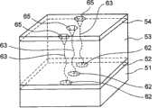
首先,如图4B所示,利用CVD(化学气相生长)或溅射法,在图4A所示的蓝宝石基板51上形成厚度为200nm的SiO2膜61。在此,对于该SiO2膜61的成膜方法不做特别的限定,若采用CVD法,则能够采用热CVD法、等离子体CVD法等。此外,所述成膜方法也可以采用溅射法。在该实施方式中,作为一个具体例,所述SiO2膜61的成膜方法采用了使用SiH4和氧气的等离子体CVD法。First, as shown in FIG. 4B, a SiO2 film 61 is formed to a thickness of 200 nm on the
接着,如图4C所示,在所述SiO2膜61上利用抗蚀剂进行构图,以在成为栅极电极正下方的区域形成由所述抗蚀剂构成的多个点状的掩模图案73。该多个点状的掩模图案73规则地排成一列。接着,如图4D所示,将所述掩模图案73作为蚀刻掩模利用缓冲氢氟酸进行蚀刻,在成为栅极电极正下方的区域以点状残留SiO2膜62。利用为了在蓝宝石基板51上选择生长而构图的掩模材料,该点状的SiO2膜62构成表面加工部。Next, as shown in FIG. 4C, patterning is performed on theSiO2
接着,如图4E所示,作为Ga原料气体使用TEG(三乙基镓),在残留了点状SiO2膜62的蓝宝石基板51上,在基板温度550℃的条件下,使低温生长GaN缓冲层52生长到50nm的厚度。然后,在基板温度1150℃的条件下,使作为第一氮化物类Ⅲ-Ⅴ族化合物半导体层的第一GaN层53生长到3μm的厚度。此时,从与蓝宝石基板51上的GaN缓冲层52相接的底面横向生长的第一GaN层53,在作为表面加工部的点状SiO2膜62的大致中央部分融合时形成贯通位错63。该贯通位错63与形成在所述底面的位错不同,在生长过程中不会消失。另外,该第一GaN层53通过在基板温度1150℃的条件下生长,不生成以所述贯通位错63为核的V缺陷。通过使所述第一GaN层53的生长温度设定在1000℃以上,能够防止凹坑形成在第一GaN层53中。Next, as shown in FIG. 4E , using TEG (triethylgallium) as the Ga source gas, on the
接着,如图4F所示,在所述第一GaN层53上,在基板温度850℃的温度下,使作为第二氮化物类Ⅲ-Ⅴ族化合物半导体层的第二GaN层54生长到50nm的厚度。由此,在该第二GaN层54上形成以所述贯通位错63为核的V形非生长区域即V缺陷65。该V缺陷65在面内方向的大小约为27nm。另外,与所述基板温度的下限不足700℃的情况相比,或者与所述基板温度的上限超过900℃的情况相比,通过使所述第二GaN层54在基板温度850℃的条件下生长,能够在所述第二GaN层54上容易地形成V缺陷65。Next, as shown in FIG. 4F , on the
另外,通过将所述第二GaN层54的层厚形成为100nm以下,能够在尽量使结晶性差的区域较薄的基础上可靠地形成V缺陷65。即,低温生长的第二GaN层54与其前后制成的层(第一、第三GaN层53,55)相比结晶性差。In addition, by forming the layer thickness of the
另外,在使所述第二GaN层54生长时,作为Ⅲ族的有机金属原料,优选采用具有乙基的有机金属。此时,能够避免发生大量的碳被掺杂在第二GaN层54中的不良现象。即,在使用具有乙基的有机金属(三乙基镓(TEG)、三乙基铝(TEA))使第二GaN层54低温生长的情况下,大量的碳被掺杂在第二GaN层54中的不良现象不会发生。In addition, when growing the
然后,如图5所述,以不填埋所述第二GaN层54的V缺陷65的方式,在基板温度1000℃的条件下,使GaN仅生长1μm的厚度,形成作为第三氮化物类Ⅲ-Ⅴ族化合物半导体层的第三GaN层55。该第三GaN层55成为结晶性改善GaN层。通过在基板温度1000℃的条件下使该第三GaN层55生长,生成不填埋V缺陷65并且与所述V缺陷65相连接的非生长区域G51,但不生成与所述V缺陷65不同的新的V缺陷。另外,通过在所述第二GaN层54上形成所述第三GaN层55,由V缺陷65和非生长区域G51构成的延长V缺陷在面内方向的大小被扩大到约0.56μm。Then, as shown in FIG. 5 , in such a way that the
另外,通过将所述第三GaN层55的生长温度的下限温度设定在950℃,即使产生少量的凹坑,也能够做到在第三GaN层55上不生长新的V缺陷。另外,通过将所述生长温度的上限温度设定在1100℃,根据促进横向生长,能够做到V缺陷65不被填埋。In addition, by setting the lower limit temperature of the growth temperature of the
接着,使AlGaN势垒层56生长。该AlGaN势垒层56为Al的组分为25%、层厚为25nm。该AlGaN势垒层56具有薄层部56a和平坦部56b,其中,薄层部56a沿着所述V缺陷65及与V缺陷65相连接的非生长区域G51形成,平坦部56b与该薄层部56a相连接并形成在V缺陷65之外,厚度比薄层部56a厚。Next, the
由此,形成图5的剖面图所示的本实施方式的层结构。这样,由所述AlGaN势垒层56和第三GaN层55构成异质结,在该AlGaN势垒层56的平坦部56b与所述第三GaN层55的界面形成浓度约为8×1012cm-2的二维电子气72。另外,所述第一至第三GaN层53~55构成沟道层60。Thereby, the layer structure of this embodiment shown in the cross-sectional view of FIG. 5 is formed. In this way, a heterojunction is formed by the
然后,在所述层结构上,利用抗蚀剂进行构图以形成源极电极57和漏极电极58。作为构成该源极电极57、漏极电极58的欧姆电极金属,能够采用Hf/Al/Hf/Au、Ti/Al/Mo/Au。另外,形成源极电极57、漏极电极58时的热处理条件随着金属的膜厚不同而不同,在该实施方式中将该热处理条件设定为在800℃下进行一分钟。Then, on the layer structure, patterning is performed using a resist to form
接着,如图5所示,对沉积栅极电极59的区域进行构图,以在所述AlGaN势垒层56上形成栅极电极59,完成该实施方式的场效应晶体管。另外,作为栅极电极59的材料,能够采用Pt、Ni、Pd、WN(氮化钨)等,在该实施方式中采用了WN。Next, as shown in FIG. 5 , the region where the
这样形成的晶体管进行夹断电压为0V的常闭动作。另外,由于所述势垒层56的薄层部56a形成在所述V缺陷65及与所述V缺陷65相连接的非生长区域G51上,因此,不进行蚀刻也能够使该薄层部56a的厚度比平坦部56b的厚度薄。因此,根据该实施方式,不会由于蚀刻损伤造成沟道迁移率下降,能够避免导通电阻的增大。另外,根据所述晶体管的制造方法,由于通过在所述蓝宝石基板51上对掩模材料SiO2进行构图,形成作为表面加工部的点状SiO2膜,因此,无需对基板51进行蚀刻也能够维持基板表面的平坦性。即,在对基板表面进行干式蚀刻加工时,不可避免地会在基板51的表面产生加工粗糙。另外,根据所述制造方法,与通过利用干式蚀刻的加工来形成表面加工部的情况相比,能够对表面加工部进行更加精细的构图。另外,通过将构成作为表面加工部的点状SiO2膜62的、用于选择生长的掩模材料设为氧化硅(SiO2),由于在所述点状SiO2膜62上难以沉积GaN,因此在所述点状的SiO2膜62上容易进行选择生长。The transistor thus formed performs a normally closed operation with a pinch-off voltage of 0V. In addition, since the
另外,在所述实施方式中,作为基板采用了蓝宝石基板,但是,作为所述基板,也可以采用碳化硅(SiC)或GaN等氮化物类Ⅲ-Ⅴ族化合物半导体层。In addition, in the above-described embodiment, a sapphire substrate is used as the substrate, but a nitride-based III-V group compound semiconductor layer such as silicon carbide (SiC) or GaN may also be used as the substrate.
(第三实施方式)(third embodiment)
在本发明的第三实施方式中,与前述的第一实施方式或第二实施方式相比,增加了如下工序。即、在将栅极电极9,59形成在AlGaN势垒层6,56上之前,将由SiO2(厚度为10nm)构成的栅极绝缘膜(未图示)沉积在AlGaN势垒层6,56上,然后,沉积栅极电极9,59。由此,能够制造作为该第三实施方式的MIS型FET。除了制造构成所述栅极绝缘膜的SiO2之外,该第三实施方式的其他制造条件与前述的第一实施方式或第二实施方式中叙述的制造条件相同。In the third embodiment of the present invention, compared with the aforementioned first embodiment or second embodiment, the following steps are added. That is, before forming the
根据该第三实施方式,与未形成有该栅极绝缘膜的情况相比,通过形成所述栅极绝缘膜,能够使夹断电压增大,因此适于电路应用。作为一个具体例,通过形成所述栅极绝缘膜,使夹断电压上升到约+3V,能够实现更好的常闭动作。According to the third embodiment, since the pinch-off voltage can be increased by forming the gate insulating film compared to the case where the gate insulating film is not formed, it is suitable for circuit applications. As a specific example, by forming the gate insulating film, the pinch-off voltage can be increased to about +3V, thereby realizing better normally-off operation.
以上说明了本发明的实施方式,但是不言而喻,可以对实施方式进行各种变更。这样的变更不应视为脱离了本发明的精神和范围,本领域技术人员根据所掌握的知识能够理解的所有变更都包含在权利要求的保护范围中。As mentioned above, although embodiment of this invention was described, it goes without saying that various changes can be made to embodiment. Such changes should not be regarded as departing from the spirit and scope of the present invention, and all changes that can be understood by those skilled in the art based on the knowledge they have mastered are included in the protection scope of the claims.
Claims (15)
Applications Claiming Priority (2)
| Application Number | Priority Date | Filing Date | Title |
|---|---|---|---|
| JP128802/09 | 2009-05-28 | ||
| JP2009128802AJP4786730B2 (en) | 2009-05-28 | 2009-05-28 | Field effect transistor and manufacturing method thereof |
Publications (2)
| Publication Number | Publication Date |
|---|---|
| CN101901834A CN101901834A (en) | 2010-12-01 |
| CN101901834Btrue CN101901834B (en) | 2012-04-25 |
Family
ID=43219246
Family Applications (1)
| Application Number | Title | Priority Date | Filing Date |
|---|---|---|---|
| CN201010194163XAExpired - Fee RelatedCN101901834B (en) | 2009-05-28 | 2010-05-28 | Field effect transistor and method for manufacturing the same |
Country Status (3)
| Country | Link |
|---|---|
| US (1) | US20100301393A1 (en) |
| JP (1) | JP4786730B2 (en) |
| CN (1) | CN101901834B (en) |
Families Citing this family (13)
| Publication number | Priority date | Publication date | Assignee | Title |
|---|---|---|---|---|
| KR101845508B1 (en) | 2011-04-27 | 2018-04-05 | 삼성전자주식회사 | Method of manufacturing semiconductor device |
| JP5883331B2 (en)* | 2012-01-25 | 2016-03-15 | 住友化学株式会社 | Method of manufacturing nitride semiconductor epitaxial wafer and method of manufacturing field effect nitride transistor |
| WO2013147710A1 (en)* | 2012-03-29 | 2013-10-03 | Agency For Science, Technology And Research | Iii-nitride high electron mobility transistor structures and methods for fabrication of same |
| US8603898B2 (en)* | 2012-03-30 | 2013-12-10 | Applied Materials, Inc. | Method for forming group III/V conformal layers on silicon substrates |
| KR20140066015A (en) | 2012-11-22 | 2014-05-30 | 삼성전자주식회사 | Hetero junction field effect transistor and method for manufacturing the same |
| WO2014167876A1 (en)* | 2013-04-12 | 2014-10-16 | シャープ株式会社 | Nitride semiconductor device |
| ITUB20155536A1 (en) | 2015-11-12 | 2017-05-12 | St Microelectronics Srl | NORMALLY OFF TYPE HEMT TRANSISTOR INCLUDING A TRINCE CONTAINING A REGION OF GATE AND FORMER AT LEAST ONE STEP, AND ITS PROCESS OF MANUFACTURE |
| CN105489725B (en)* | 2016-01-25 | 2018-10-16 | 厦门市三安光电科技有限公司 | A kind of LED chip structure and production method |
| US10818778B2 (en)* | 2017-11-27 | 2020-10-27 | Taiwan Semiconductor Manufacturing Co., Ltd. | Heterogeneous semiconductor device substrates with high quality epitaxy |
| CN108735601B (en)* | 2018-04-16 | 2021-04-16 | 厦门市三安集成电路有限公司 | HEMT fabricated by in-situ growth of patterned barrier layer and method thereof |
| CN111816704A (en)* | 2020-08-18 | 2020-10-23 | 松山湖材料实验室 | A kind of nano switch device and preparation method thereof |
| CN112397571B (en)* | 2021-01-18 | 2021-04-23 | 苏州纳维科技有限公司 | A kind of gallium nitride substrate and semiconductor composite substrate |
| CN118738242A (en)* | 2023-03-30 | 2024-10-01 | 宸明科技股份有限公司 | Semiconductor component and method for manufacturing the same |
Family Cites Families (12)
| Publication number | Priority date | Publication date | Assignee | Title |
|---|---|---|---|---|
| JP3201475B2 (en)* | 1998-09-14 | 2001-08-20 | 松下電器産業株式会社 | Semiconductor device and method of manufacturing the same |
| JP3801125B2 (en)* | 2001-10-09 | 2006-07-26 | 住友電気工業株式会社 | Single crystal gallium nitride substrate, method for crystal growth of single crystal gallium nitride, and method for manufacturing single crystal gallium nitride substrate |
| US7105865B2 (en)* | 2001-09-19 | 2006-09-12 | Sumitomo Electric Industries, Ltd. | AlxInyGa1−x−yN mixture crystal substrate |
| US20080006201A1 (en)* | 2001-09-19 | 2008-01-10 | Sumitomo Electric Industries, Ltd. | Method of growing gallium nitride crystal |
| JP3968566B2 (en)* | 2002-03-26 | 2007-08-29 | 日立電線株式会社 | Nitride semiconductor crystal manufacturing method, nitride semiconductor wafer, and nitride semiconductor device |
| JP4559190B2 (en)* | 2003-11-06 | 2010-10-06 | 昭和電工株式会社 | Compound semiconductor device |
| JP2007048842A (en)* | 2005-08-08 | 2007-02-22 | Toshiba Corp | Nitride semiconductor device |
| US7691732B2 (en)* | 2008-06-18 | 2010-04-06 | Sumitomo Electric Industries, Ltd. | Manufacturing method of nitride substrate, nitride substrate, and nitride-based semiconductor device |
| JP5261945B2 (en)* | 2007-02-23 | 2013-08-14 | サンケン電気株式会社 | Field effect semiconductor device and manufacturing method thereof |
| JP5245305B2 (en)* | 2007-07-06 | 2013-07-24 | サンケン電気株式会社 | Field effect semiconductor device and manufacturing method thereof |
| JP5487550B2 (en)* | 2007-08-29 | 2014-05-07 | サンケン電気株式会社 | Field effect semiconductor device and manufacturing method thereof |
| JP5306904B2 (en)* | 2009-05-28 | 2013-10-02 | シャープ株式会社 | Nitride semiconductor light emitting diode device and method for manufacturing the same |
- 2009
- 2009-05-28JPJP2009128802Apatent/JP4786730B2/ennot_activeExpired - Fee Related
- 2010
- 2010-05-27USUS12/788,872patent/US20100301393A1/ennot_activeAbandoned
- 2010-05-28CNCN201010194163XApatent/CN101901834B/ennot_activeExpired - Fee Related
Also Published As
| Publication number | Publication date |
|---|---|
| JP4786730B2 (en) | 2011-10-05 |
| US20100301393A1 (en) | 2010-12-02 |
| JP2010278199A (en) | 2010-12-09 |
| CN101901834A (en) | 2010-12-01 |
Similar Documents
| Publication | Publication Date | Title |
|---|---|---|
| CN101901834B (en) | Field effect transistor and method for manufacturing the same | |
| US10566450B2 (en) | Normally-off HEMT transistor with selective generation of 2DEG channel, and manufacturing method thereof | |
| JP5323527B2 (en) | Manufacturing method of GaN-based field effect transistor | |
| CN103137681B (en) | There is the circuit structure of the islands between source electrode and drain electrode | |
| JP5653607B2 (en) | GaN-based field effect transistor and manufacturing method thereof | |
| TWI431770B (en) | Semiconductor device and method of manufacturing the same | |
| JP5634681B2 (en) | Semiconductor element | |
| CN103548127B (en) | Semiconductor device and manufacturing method thereof | |
| JP7013710B2 (en) | Manufacturing method of nitride semiconductor transistor | |
| JP2006286942A (en) | Semiconductor device and manufacturing method thereof | |
| JP2009099691A (en) | Method of manufacturing field-effect semiconductor device | |
| JPWO2005015642A1 (en) | Semiconductor device and manufacturing method thereof | |
| JP2007165431A (en) | Field effect transistor and manufacturing method thereof | |
| JP2010166027A (en) | GaN-BASED FIELD-EFFECT TRANSISTOR AND METHOD OF MANUFACTURING THE SAME | |
| JP2008010526A (en) | Nitride semiconductor device, and its manufacturing method | |
| CN105470294A (en) | Vertical gallium nitride power switch device and manufacturing method therefor | |
| KR20190112523A (en) | Heterostructure Field Effect Transistor and production method thereof | |
| CN113628962B (en) | III-nitride enhanced HEMT device and manufacturing method thereof | |
| US8283700B2 (en) | Field effect transistor and manufacturing method thereof | |
| JP4869563B2 (en) | Nitride semiconductor device and manufacturing method thereof | |
| JP2011129607A (en) | Gan-based mos field-effect transistor | |
| JP2010165783A (en) | Field effect transistor, and method of manufacturing the same | |
| JP5460016B2 (en) | Semiconductor device and manufacturing method thereof | |
| CN205231071U (en) | Perpendicular type gallium nitride power switch device | |
| TW202406146A (en) | High electron mobility transistor and method for fabricating the same |
Legal Events
| Date | Code | Title | Description |
|---|---|---|---|
| C06 | Publication | ||
| PB01 | Publication | ||
| C10 | Entry into substantive examination | ||
| SE01 | Entry into force of request for substantive examination | ||
| C14 | Grant of patent or utility model | ||
| GR01 | Patent grant | ||
| CF01 | Termination of patent right due to non-payment of annual fee | Granted publication date:20120425 Termination date:20150528 | |
| EXPY | Termination of patent right or utility model |