CN101901090B - Display device - Google Patents
Display deviceDownload PDFInfo
- Publication number
- CN101901090B CN101901090BCN2009102249963ACN200910224996ACN101901090BCN 101901090 BCN101901090 BCN 101901090BCN 2009102249963 ACN2009102249963 ACN 2009102249963ACN 200910224996 ACN200910224996 ACN 200910224996ACN 101901090 BCN101901090 BCN 101901090B
- Authority
- CN
- China
- Prior art keywords
- electrode
- electrodes
- block
- display device
- thin line
- Prior art date
- Legal status (The legal status is an assumption and is not a legal conclusion. Google has not performed a legal analysis and makes no representation as to the accuracy of the status listed.)
- Active
Links
Images


Classifications
- G—PHYSICS
- G06—COMPUTING OR CALCULATING; COUNTING
- G06F—ELECTRIC DIGITAL DATA PROCESSING
- G06F3/00—Input arrangements for transferring data to be processed into a form capable of being handled by the computer; Output arrangements for transferring data from processing unit to output unit, e.g. interface arrangements
- G06F3/01—Input arrangements or combined input and output arrangements for interaction between user and computer
- G06F3/03—Arrangements for converting the position or the displacement of a member into a coded form
- G06F3/041—Digitisers, e.g. for touch screens or touch pads, characterised by the transducing means
- G06F3/044—Digitisers, e.g. for touch screens or touch pads, characterised by the transducing means by capacitive means
- G06F3/0446—Digitisers, e.g. for touch screens or touch pads, characterised by the transducing means by capacitive means using a grid-like structure of electrodes in at least two directions, e.g. using row and column electrodes
- G—PHYSICS
- G06—COMPUTING OR CALCULATING; COUNTING
- G06F—ELECTRIC DIGITAL DATA PROCESSING
- G06F3/00—Input arrangements for transferring data to be processed into a form capable of being handled by the computer; Output arrangements for transferring data from processing unit to output unit, e.g. interface arrangements
- G06F3/01—Input arrangements or combined input and output arrangements for interaction between user and computer
- G06F3/03—Arrangements for converting the position or the displacement of a member into a coded form
- G06F3/041—Digitisers, e.g. for touch screens or touch pads, characterised by the transducing means
- G06F3/044—Digitisers, e.g. for touch screens or touch pads, characterised by the transducing means by capacitive means
- G—PHYSICS
- G06—COMPUTING OR CALCULATING; COUNTING
- G06F—ELECTRIC DIGITAL DATA PROCESSING
- G06F3/00—Input arrangements for transferring data to be processed into a form capable of being handled by the computer; Output arrangements for transferring data from processing unit to output unit, e.g. interface arrangements
- G06F3/01—Input arrangements or combined input and output arrangements for interaction between user and computer
- G06F3/03—Arrangements for converting the position or the displacement of a member into a coded form
- G06F3/041—Digitisers, e.g. for touch screens or touch pads, characterised by the transducing means
- G06F3/0412—Digitisers structurally integrated in a display
- G—PHYSICS
- G06—COMPUTING OR CALCULATING; COUNTING
- G06F—ELECTRIC DIGITAL DATA PROCESSING
- G06F3/00—Input arrangements for transferring data to be processed into a form capable of being handled by the computer; Output arrangements for transferring data from processing unit to output unit, e.g. interface arrangements
- G06F3/01—Input arrangements or combined input and output arrangements for interaction between user and computer
- G06F3/03—Arrangements for converting the position or the displacement of a member into a coded form
- G06F3/041—Digitisers, e.g. for touch screens or touch pads, characterised by the transducing means
- G06F3/044—Digitisers, e.g. for touch screens or touch pads, characterised by the transducing means by capacitive means
- G06F3/0445—Digitisers, e.g. for touch screens or touch pads, characterised by the transducing means by capacitive means using two or more layers of sensing electrodes, e.g. using two layers of electrodes separated by a dielectric layer
- G—PHYSICS
- G06—COMPUTING OR CALCULATING; COUNTING
- G06F—ELECTRIC DIGITAL DATA PROCESSING
- G06F3/00—Input arrangements for transferring data to be processed into a form capable of being handled by the computer; Output arrangements for transferring data from processing unit to output unit, e.g. interface arrangements
- G06F3/01—Input arrangements or combined input and output arrangements for interaction between user and computer
- G06F3/03—Arrangements for converting the position or the displacement of a member into a coded form
- G06F3/041—Digitisers, e.g. for touch screens or touch pads, characterised by the transducing means
- G06F3/044—Digitisers, e.g. for touch screens or touch pads, characterised by the transducing means by capacitive means
- G06F3/0447—Position sensing using the local deformation of sensor cells
- G—PHYSICS
- G06—COMPUTING OR CALCULATING; COUNTING
- G06F—ELECTRIC DIGITAL DATA PROCESSING
- G06F2203/00—Indexing scheme relating to G06F3/00 - G06F3/048
- G06F2203/041—Indexing scheme relating to G06F3/041 - G06F3/045
- G06F2203/04111—Cross over in capacitive digitiser, i.e. details of structures for connecting electrodes of the sensing pattern where the connections cross each other, e.g. bridge structures comprising an insulating layer, or vias through substrate
Landscapes
- Engineering & Computer Science (AREA)
- General Engineering & Computer Science (AREA)
- Theoretical Computer Science (AREA)
- Human Computer Interaction (AREA)
- Physics & Mathematics (AREA)
- General Physics & Mathematics (AREA)
- Position Input By Displaying (AREA)
- Liquid Crystal (AREA)
Abstract
Translated fromChineseDescription
Translated fromChinese本申请要求2008年11月26日提交的日本专利申请JP2008-300678之优先权,该专利申请的内容通过引用而结合于本申请。This application claims priority from Japanese Patent Application JP2008-300678 filed on November 26, 2008, the contents of which are incorporated herein by reference.
技术领域technical field
本发明涉及将坐标输入屏幕的输入装置及具有该输入装置的显示装置,尤其适用于具有电容耦合式输入装置的显示装置中的坐标检测精度的高精度化。The present invention relates to an input device for inputting coordinates on a screen and a display device having the input device, and is particularly suitable for high accuracy of coordinate detection in a display device having a capacitive coupling input device.
背景技术Background technique
PDA或便携终端等移动电子设备、各种家电产品、无人受理机等的固定型顾客引导终端使用具有具备屏幕输入功能的输入装置(以下也称为触摸传感器或触摸屏)的显示装置,使用者用手指等在显示屏幕上进行触摸操作(触压操作,以下简称为触摸)来输入信息。作为进行这样的触摸的输入装置,已知有检测触摸部分的电阻值变化的电阻膜方式或检测电容变化的静电电容耦合方式或检测由于触摸而被遮蔽的部分的光量变化的光传感器方式等。Stationary customer guidance terminals such as mobile electronic devices such as PDAs and portable terminals, various home appliances, and unmanned reception machines use a display device with an input device (hereinafter also referred to as a touch sensor or touch screen) with a screen input function. Information is input by performing a touch operation (touch pressure operation, hereinafter simply referred to as touch) on the display screen with a finger or the like. As an input device that performs such a touch, there are known a resistive film method that detects a change in resistance value of a touched portion, a capacitive coupling method that detects a change in capacitance, or a photosensor method that detects a change in light intensity of a portion blocked by a touch.
静电电容耦合方式与电阻膜方式或光传感器方式相比具有如下优点。例如,相对于电阻膜方式或光传感器方式的低至80%的透过率,静电电容耦合方式的透过率高达约90%,具有不使显示画面品质降低的优势。另外,由于电阻膜方式通过电阻膜的机械接触来探知触摸位置,存在电阻膜劣化或破损之可能性,而静电电容耦合方式则无检测用电极与其他电极等接触的机械接触,有利于耐久性的改善。The capacitive coupling method has the following advantages over the resistive film method or the photosensor method. For example, the transmittance of the capacitive coupling method is as high as about 90% compared to the low transmittance of 80% for the resistive film method or the photosensor method, and has the advantage of not deteriorating the quality of the display screen. In addition, since the resistive film method detects the touch position through the mechanical contact of the resistive film, there is a possibility of deterioration or damage of the resistive film, while the electrostatic capacitive coupling method has no mechanical contact between the detection electrode and other electrodes, which is beneficial to durability improvement.
作为静电电容耦合方式的触摸屏,例如有如下述专利文献1所公开的方式。在所公开的方式中,具有纵横二维矩阵状配置的检测用纵向电极(X电极)和检测用横向电极(Y电极),并用输入处理部检测各电极的电容。由于用手指等导体接触触摸屏的表面时各电极的电容增加,输入处理部检测到该电容增加,并基于各电极探知的电容变化的信号计算出输入坐标。这里,即使检测用电极的电阻值这一物理特性因电极劣化而改变,也很少影响到电容检测,因此对触摸屏的输入位置检测精度的影响小。所以,能够实现高精度的输入位置检测。As a capacitive coupling type touch panel, for example, there is a type disclosed in
再有,与本申请发明关联的在先的技术文献有日本特表2003-511799号公报。In addition, the prior technical document related to the invention of the present application includes JP-A-2003-511799.
但是,如上述专利文献1所记载,由于静电电容耦合方式的触摸屏通过检测各检测用电极的电容变化来检测输入坐标,作为输入工具其前提条件是使用导电性材料。因此,如果用电阻膜方式等使用的非导电性的树脂制触笔等接触静电电容耦合方式的触摸屏,电极的电容几乎不发生变化,因此有检测不到输入坐标的问题。However, as described in the above-mentioned
另外,在2点同时地将树脂制触笔等接触静电电容耦合方式的触摸屏的使用方法中,由于要检测2个X坐标和2个Y坐标,作为接触点的候选点要考虑4个坐标,因此难以检测2点同时地接触的点。In addition, in the method of using a capacitive coupling type touch panel with a resin stylus at two points at the same time, since two X coordinates and two Y coordinates are to be detected, four coordinates are considered as candidates for contact points. Therefore, it is difficult to detect a point where two points touch at the same time.
还有,在对应于小接触面的输入工具时,不增加电极数地进行高精度检测的方法也是一个问题。In addition, in the case of an input tool with a small contact surface, a method of performing high-precision detection without increasing the number of electrodes is also a problem.
发明内容Contents of the invention
本发明为解决上述以往技术的问题而提出,其目的在于提供如下一种技术:在具有静电电容耦合方式的触摸屏的显示装置中,对于非导电性的输入工具的触摸也可作出反应,且即使触摸面积小也可用少量的电极条数实现高精度位置检测。The present invention is made to solve the problems of the above-mentioned conventional technologies, and its object is to provide a technology that can respond to the touch of a non-conductive input tool in a display device having a touch panel of an electrostatic capacitive coupling method, and even The small touch area can also realize high-precision position detection with a small number of electrodes.
本发明的上述及其他目的及新颖特征,通过本说明书的记载及附图阐述。The above and other objects and novel features of the present invention are explained by the description of this specification and the accompanying drawings.
以下,对于本申请公开的发明,就其典型部件的概要作如下的简要说明。Hereinafter, the invention disclosed in this application will be briefly described as follows in terms of the outline of its typical components.
为了解决上述课题,本发明使用具有多个X电极、多个Y电极和多个Z电极的静电电容触摸屏。该静电电容触摸屏中,上述X电极和上述Y电极隔着第1绝缘层相交叉,各自在其延伸方向上以块区部与细线部交互排列而形成,在平面上看,上述X电极的块区部和上述Y电极的块区部不相重叠地配置。In order to solve the above-mentioned problems, the present invention uses a capacitive touch panel having a plurality of X electrodes, a plurality of Y electrodes, and a plurality of Z electrodes. In this electrostatic capacitive touch screen, the above-mentioned X electrodes and the above-mentioned Y electrodes intersect with each other through the first insulating layer, and are formed by alternately arranging block regions and thin line portions in the direction of their extension. The block portion and the block portion of the Y electrode are arranged so as not to overlap each other.
另外,其特征在于,在平面上看,上述Z电极隔着第2绝缘层与相邻的上述X电极和上述Y电极两者重叠而形成,且上述Z电极在电气上相互浮置。此时,通过用厚度因触摸按压而变化的材料、例如弹性绝缘材料形成上述第2绝缘层,非导电性的输入工具也能使上述X电极及上述Y电极与上述Z电极之间发生电容变化,能够以静电电容耦合方式检测触摸。In addition, the Z electrode is formed to overlap both the adjacent X electrode and the Y electrode in a planar view, and the Z electrodes are electrically floating to each other. At this time, by forming the second insulating layer with a material whose thickness changes due to touch and pressure, such as an elastic insulating material, a non-conductive input tool can also change the capacitance between the X electrode, the Y electrode, and the Z electrode. , can detect touch by electrostatic capacitive coupling.
另外,其特征在于,上述X电极的块区部延伸到与该X电极相邻的X电极的细线部附近,在平面上看,该X电极的块区部中的形状是:在上述相邻的X电极的细线部附近面积成为最小,在该X电极的细线部附近面积成为最大,从该X电极的细线部附近开始直至上述相邻的X电极的细线部附近,该块区部的面积减少。从而,即使在上述X电极的电极间隔比触摸操作中的接触面宽的情况下,也可根据相邻的上述X电极的检测电容分量之比计算出触摸坐标位置,能够用少量的电极条数进行高精度的位置检测。In addition, it is characterized in that the block portion of the X electrode extends to the vicinity of the thin line portion of the X electrode adjacent to the X electrode, and the shape of the block portion of the X electrode in plan view is: The area near the thin line portion of the adjacent X electrode becomes the smallest, and the area near the thin line portion of the X electrode becomes the largest. From the vicinity of the thin line portion of the X electrode to the vicinity of the thin line portion of the adjacent X electrode, the The area of the block portion is reduced. Therefore, even if the electrode interval of the above-mentioned X electrodes is wider than the contact surface in the touch operation, the touch coordinate position can be calculated from the ratio of the detection capacitance components of the adjacent X electrodes, and a small number of electrodes can be used. High-precision position detection is performed.
另外,通过将上述多个Z电极与相邻的上述X电极和上述Y电极两者相重叠而形成,在上述X电极上存在因触摸产生的接触面时也能通过上述Z电极检测到相邻的上述Y电极的电容变化,相反地,在上述Y电极上存在因触摸产生的接触面时也能通过上述Z电极检测到相邻的上述X电极的电容变化,因此能够在整个触摸屏上检测输入坐标。同时,也使上述Y电极的电极条数的削减成为可能。In addition, by forming the plurality of Z electrodes overlapping both the adjacent X electrodes and the Y electrodes, even when there is a contact surface caused by a touch on the X electrodes, the adjacent electrodes can be detected by the Z electrodes. On the contrary, when there is a contact surface caused by touch on the above-mentioned Y electrode, the capacitance change of the adjacent above-mentioned X electrode can also be detected through the above-mentioned Z electrode, so the input can be detected on the entire touch screen coordinate. At the same time, it is also possible to reduce the number of Y electrodes described above.
另外,在X电极或Y电极中的一方电极上依次施加信号,用另一方电极检测信号的变化,从而预先判别是在哪个电极上施加的信号,提高了在静电电容耦合方式的触摸屏上同时接触2点时的检测精度。In addition, a signal is sequentially applied to one of the X electrodes or the Y electrodes, and the change of the signal is detected by the other electrode, so as to determine in advance which electrode the signal is applied on, which improves the simultaneous touch on the touch screen of the electrostatic capacitance coupling method. Detection accuracy at 2 o'clock.
根据本发明,通过在触摸屏的电极的形状和配置上设法改进,能够用少量的电极条数以高于以往技术的精度进行位置检测。另外,在同时接触2点的情况下也能提高检测精度。According to the present invention, by trying to improve the shape and arrangement of the electrodes of the touch panel, it is possible to perform position detection with a small number of electrodes with higher precision than the conventional technology. In addition, detection accuracy can be improved even when two points are in contact at the same time.
附图说明Description of drawings
图1是具有本发明实施例的静电电容耦合方式的触摸屏的显示装置的概略结构图。FIG. 1 is a schematic configuration diagram of a display device having a capacitive coupling touch panel according to an embodiment of the present invention.
图2是表示本发明实施例的显示装置的电容检测部的电路结构的方块图。2 is a block diagram showing a circuit configuration of a capacitance detection unit of a display device according to an embodiment of the present invention.
图3是说明本发明实施例的显示装置的电容检测部的动作的时序图。3 is a timing chart illustrating the operation of a capacitance detection unit of the display device according to the embodiment of the present invention.
图4表示本发明实施例的显示装置的电容检测时检测值的存储状态。FIG. 4 shows the storage state of detected values during capacitance detection of the display device according to the embodiment of the present invention.
图5是表示本发明实施例的静电电容耦合方式的触摸屏的电极形状的概略平面图。5 is a schematic plan view showing electrode shapes of a capacitive coupling touch panel according to an embodiment of the present invention.
图6是表示本发明实施例的静电电容耦合方式的触摸屏的电极结构的要部剖视图。6 is a cross-sectional view of main parts showing an electrode structure of a capacitive coupling touch panel according to an embodiment of the present invention.
图7是表示本发明实施例的静电电容耦合方式的触摸屏中因人的手指等的触摸操作导致电容变化的示意图。FIG. 7 is a schematic diagram showing a change in capacitance due to a touch operation by a human finger or the like in a touch panel of an electrostatic capacitive coupling method according to an embodiment of the present invention.
图8是表示本发明实施例的静电电容耦合方式的触摸屏中因压力检测用绝缘层的厚度变化导致电容变化的示意图。FIG. 8 is a schematic diagram showing a change in capacitance due to a change in the thickness of the insulating layer for pressure detection in the touch panel of the capacitive coupling method according to the embodiment of the present invention.
图9是表示本发明实施例的静电电容耦合方式的触摸屏中接触面在X方向移动时的接触位置的概略平面图。9 is a schematic plan view showing the contact position when the contact surface moves in the X direction in the capacitive coupling touch panel according to the embodiment of the present invention.
图10是表示本发明实施例的静电电容耦合方式的触摸屏的电极形状的变形例的概略平面图。10 is a schematic plan view showing a modified example of electrode shape of the capacitive coupling touch panel according to the embodiment of the present invention.
图11是表示本发明实施例的静电电容耦合方式的触摸屏的电极形状的变形例的概略平面图。11 is a schematic plan view showing a modified example of electrode shape of the capacitive coupling touch panel according to the embodiment of the present invention.
图12是表示本发明实施例的静电电容耦合方式的触摸屏的截面结构的概略图。12 is a schematic diagram showing a cross-sectional structure of a capacitive coupling type touch panel according to an embodiment of the present invention.
具体实施方式Detailed ways
以下,参照附图详细说明本发明的实施例。Hereinafter, embodiments of the present invention will be described in detail with reference to the drawings.
再有,在说明实施例的全部附图中,具有相同功能的部件使用相同的附图标记,省略对该部件的重复说明。Note that, in all the drawings for explaining the embodiments, components having the same functions are denoted by the same reference numerals, and repeated description of these components will be omitted.
输入装置(以下称触摸屏)及具有该装置的显示装置的构成如图1所示。图1中,101是基于本发明的实施例的触摸屏。The configuration of an input device (hereinafter referred to as a touch panel) and a display device having the device is shown in FIG. 1 . In FIG. 1 , 101 is a touch screen based on the embodiment of the present invention.
触摸屏101具有电容检测用的X电极XP和Y电极YP。这里,图示了例如X电极4条(XP1至XP4)、Y电极4条(YP1至YP4),但电极数并不限于此。The
触摸屏101设置在显示装置106的前面。因此,使用者观看显示装置上显示的图像时,显示图像须透过触摸屏,因此触摸屏最好具有高的光透过率。The
触摸屏101的X电极和Y电极通过检测用布线201与电容检测部102连接。电容检测部102根据控制运算部103输出的检测控制信号202执行控制,检测触摸屏所包含的各电极(X电极、Y电极)的电容,并将因各电极的电容值而变化的电容检测信号203输出到控制运算部103。The X electrodes and Y electrodes of the
控制运算部103根据各电极的电容检测信号203计算出各电极的信号分量,并根据各电极的信号分量算出输入坐标。控制运算部103通过I/F信号204将输入坐标传送给系统104。如果输入坐标通过触摸操作从触摸屏101传送到系统104,生成与该触摸操作对应的显示图像,并作为显示控制信号205传送给显示控制电路105。显示控制电路105按照由显示控制信号205传送的显示图像生成显示信号206,并在显示装置上显示图像。The
图2(A)以概略方块图表示电容检测部102的电路结构,图2(B)表示信号读出部310的概略结构。电容检测部102由给Y电极输入信号的信号输入部311、从X电极读出信号的信号读出部310及存储部312构成。FIG. 2(A) shows a schematic block diagram of the circuit configuration of the
再有,虽然图2(A)中仅以一对X电极XP1、Y电极YP1图示电路结构,应认为触摸屏101上形成的各X电极、Y电极上分别连接了具有相同结构的信号读出部310-n、信号输入部311-n。In addition, although only a pair of X electrodes XP1 and Y electrodes YP1 are used to illustrate the circuit structure in FIG. 2(A), it should be considered that the X electrodes formed on the
信号输入部311通过开关307、308的切换基准电位Vap和Vref,如波形309那样对Y电极施加电压。The
信号读出部310的构成包括:由运算放大器300、积分电容301、复位开关305组成的积分电路320;由采样开关303、保持电容302组成的采样保持电路330;电压缓冲器304;以及模数变换器306。The composition of the
以下,概略说明电容检测部102的动作。再有,假定在电容检测部102的初始状态下积分电容301处于未充电状态。Hereinafter, the operation of the
在初始状态,首先开关307成为导通状态,由信号输入部311对Y电极YP1施加电压。从而,X电极、Y电极间的耦合电容250对Y电极YP1充电,直至达到施加电压Vap。此时,X电极XP1的电位由于运算放大器300的负反馈作用而始终固定在接地电位上。因此,充电电流经由积分电容301流向运算放大器300的输出端子321。In the initial state, first, the
若设该动作施加到积分电路320的输出端子321的电压为Vo、耦合电容250的电容为Cdv、积分电容301的电容为Cr,则有Vo=-Vap(Cdv/Cr),依存于与X电极和Y电极间的耦合电容250的大小Cdv。If the voltage applied to the output terminal 321 of the integrating
通过上述动作确定了积分电路320的输出电位Vo后,将输出电位Vo用采样保持电路330保持。采样保持电路330首先将采样开关303设于导通状态,接着在经过预定时间后设于截止状态,从而将输出电位Vo保持在保持电容302中。保持电容302中保持的电位Vo经由电压缓冲器304输入到模数变换器306,变换成数字数据。After the output potential Vo of the integrating
再有,虽然采用了通过电压缓冲器304将采样保持电路330的保持电压输入模数变换器306的结构,但也是电压缓冲器304具有电压放大率的结构。Furthermore, although the
另外,与上述X电极XP1以外的X电极各自连接的信号读出部执行跟与X电极XP1连接的信号读出部310同样的动作,由来自Y电极YP1的输入信号导致的积分电路输出电位与X电极XP1同时读出。In addition, the signal readout section connected to each of the X electrodes other than the above-mentioned X electrode XP1 performs the same operation as the
与各X电极连接的信号读出部310的输出被输入存储部312,该输出数据被保持在存储部312中。存储部312与图1所示的运算控制部103之间进行保持数据的收发。The output of the
Y电极YP被依次施加信号309,逐个地对Y电极YP施加电压,并进行电容检测。另外,信号读出部310在电容检测之前将复位开关305暂设为导通状态,其后控制成截止状态,将各积分电路的积分电容301复位。The
以下,重复同样的动作。这里,通过在任意的Y电极YP上设定施加信号309的定时,并在特定的Y电极YP施加特定的期间脉冲状信号,可根据基准时钟等的计数判断X电极XP的输出是来自哪一个Y电极YP的输出信号。Thereafter, the same operation is repeated. Here, by setting the timing of applying the
图3是表示图2所示的电容检测部102的动作的时序图。信号309-1至309-n是信号输入部311-1至311-n的动作信号波形,信号输入部311-1至311-n在检测周期DTC期间依次对Y电极YP1至Ypn输出信号309。再有,以下也将信号309称为脉冲信号。FIG. 3 is a timing chart showing the operation of the
波形Icdv是流向图2所示的XY电极间耦合电容250(Cdv)的电流波形。由于信号输入部311的信号输入,在Y电极YP的电位上升时瞬态地流过电流。另外,在Y电极YP的电位下降时也瞬态地流过电流。The waveform Icdv is a waveform of a current flowing to the coupling capacitance 250 (Cdv) between XY electrodes shown in FIG. 2 . When the potential of the Y electrode YP rises due to the signal input from the
波形VIN是图2所示的积分电路320的输出波形,即对应于各脉冲信号309的上述积分电路320的输出端子321的电压Vo。另外,波形SWRST-1表示图2所示的复位开关305的控制信号波形。The waveform VIN is the output waveform of the integrating
如果复位开关控制信号SWRST-1上升,积分电路320就被复位,波形VIN下降,信号读出部310成为初始状态。之后,从信号输入部311输入脉冲信号309,积分电路320的输出波形VIN再次上升。以下,重复该动作。When the reset switch control signal SWRST-1 rises, the
再有,本例中示出了波形VIN的振幅变化的例子,但这表示每次输入信号的Y电极改变时检测的电容大小在变化。即,在触摸屏101上有检测对象接触时,反映该电容变化的信号VIN显示局部变化的情况来示出接触点。In this example, an example in which the amplitude of the waveform VIN changes is shown, but this means that the magnitude of the detected capacitance changes every time the Y electrode of the input signal changes. That is, when a detection object touches the
波形SWSH-1是控制图2所示的采样保持电路330的采样开关303的信号。另外,波形SH-1表示采样保持电路330的输出信号。在信号SWSH-1上升的时间区,采样开关303成为导通状态,保持电容302上被施加对采样保持电路330的输入电位即积分电路320的输出电位(波形VIN),如果信号SWSH-1下降,采样开关303就成为断开状态,保持电容302中保持施加电压。如波形SH-1所示,采样保持电路330的输出按每次采样动作而更新。The waveform SWSH-1 is a signal for controlling the sample switch 303 of the
波形AD-1表示控制图2所示的模数变换器306的信号,另外,波形ADout-1表示该模数变换器306的输出信号。在采样保持电路的输出波形SH-1每次更新时,设置预定时间差并发出信号AD-1。信号AD-1一被输出,模数变换器306就将其输入电压作为预定分辨率的数字数据ADout-1输出。Waveform AD-1 represents a signal for controlling the analog-to-
波形Mem-1表示图2所示的对存储部312的写入控制信号。每次信号ADout-1更新时,设置预定时间差并发出信号Mem-1。信号Mem-1一发出,数字数据ADout-1就被写入存储部312。Waveform Mem-1 represents the write control signal to the
以上,对伴随电容检测部102的动作的信号波形变化以图2所示的信号读出部310为着眼点作了说明,但与其他X电极连接的信号读出部(310-n)也成为相同的动作及波形变化。Above, the signal waveform change accompanying the operation of the
图4(A)表示通过获取定时区别图2所示的存储部312中存储的检测值,并使之与由XY电极确定的坐标对应。这里,四方形表示与横轴和纵轴所示的各电极之间交叉的位置。另外,这些四方形内的数值反映通过检测过程得到的各交点的电容值。数值越大,表示电容值越大,通过该数值的大小或阈值判断等来判断是否有检测对象对触摸屏101的接触。FIG. 4(A) shows that the detected values stored in the
图4(B)表示对上述图4(A)的状态进行阈值判断,具体就是将数值超过100的状态判断为有接触。通过分组(grouping)处理将该判断结果赋予每组共同的编号。在该处理之后,分析每组信号强度的分布,变换成检测对象对于触摸屏101的接触坐标。FIG. 4(B) shows that threshold value judgment is performed on the state in FIG. 4(A) above, specifically, a state with a value exceeding 100 is judged as being in contact. The determination result is given a common number for each group by grouping processing. After this processing, the distribution of each group of signal intensities is analyzed and transformed into contact coordinates of the detection object on the
这里的分组处理可设想为一般所知的标记(labeling)处理等,但并不受此限定。另外,根据通过上述电容检测过程得到的图4(A)所示的数据算出检测对象对触摸屏101的接触坐标的手段,显然不限于这里记载的方法。The grouping process here can be assumed to be generally known labeling (labeling) process, etc., but it is not limited to this. In addition, the method of calculating the contact coordinates of the detection object on the
接着,用图5及图6说明设于本发明实施例的触摸屏101的电容检测用电极。Next, the electrodes for capacitance detection provided on the
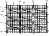
图5(A)表示触摸屏101的电容检测用的X电极XP及Y电极YP以及在其上部重叠设置的Z电极ZP的电极图案。X电极XP和Y电极YP中,例如,X电极XP通过检测用布线201与电容检测部102连接。另一方面,在一定期间在Y电极YP上施加预先确定的定时和电压的脉冲信号309。Z电极ZP不被电气连接,设于浮置状态。FIG. 5(A) shows an electrode pattern of the capacitance detection X electrode XP and Y electrode YP of the
图5(B)中仅示出X电极XP和Y电极YP的电极图案。Y电极YP在触摸屏101的横向延伸,多个Y电极YP在纵向并排。在Y电极YP和X电极XP的交叉部分,为了减小各电极的交叉电容而将Y电极YP和X电极XP的电极宽度收窄。该部分称为细线部327。因此,Y电极YP在其延伸方向上形成为细线部327与其余电极部分(以下称块区部328)交互配置的形状。Only the electrode patterns of the X electrode XP and the Y electrode YP are shown in FIG. 5(B). The Y electrodes YP extend laterally of the
在相邻的Y电极YP之间配置X电极XP。X电极XP在触摸屏101的纵向延伸,多个X电极XP在横向并排。与Y电极YP一样,X电极XP在其延伸方向上形成为细线部327与块区部328X交互配置的形状。The X electrodes XP are arranged between adjacent Y electrodes YP. The X electrodes XP extend in the longitudinal direction of the
如图5(B)所示,X电极XP的块区部328X设为菱形。在说明X电极XP的块区部328X的形状的基础上,假定用以将X电极XP连接于检测用布线的布线位置(或者X电极XP的细线部327)位于X电极XP的横向的中心。X电极XP的块区部328X的电极形状是,随着与相邻的其他X电极XP的中心接近,其面积减小,且越接近该X电极XP的中心,其面积变得越大。As shown in FIG. 5(B), the block portion 328X of the X electrode XP is formed in a rhombus shape. On the basis of describing the shape of the block portion 328X of the X electrode XP, it is assumed that the wiring position (or the thin line portion 327 of the X electrode XP) for connecting the X electrode XP to the detection wiring is located at the center of the lateral direction of the X electrode XP. . The electrode shape of the block portion 328X of the X electrode XP is such that its area decreases as it approaches the center of another adjacent X electrode XP, and its area becomes larger as it approaches the center of the X electrode XP.
因此,如果考虑相邻的2条X电极XP、例如X电极XP1和XP2之间的X电极XP的面积,则在X电极XP1的中心附近X电极XP1的块区部328X的电极面积(电极宽度)成为最大,且X电极XP2的块区部328X的电极面积(电极宽度)成为最小。另一方面,在X电极XP2的中心附近X电极XP1的块区部328X的电极面积(电极宽度)成为最小,且X电极XP2的块区部328X的电极面积(电极宽度)成为最大。这里,相邻的2条X电极XP之间的块区部328X的形状的特征是,朝相邻的X电极XP形成凸状。Therefore, if considering the area of the X electrode XP between two adjacent X electrodes XP, for example, the X electrodes XP1 and XP2, the electrode area (electrode width ) becomes the largest, and the electrode area (electrode width) of the block portion 328X of the X electrode XP2 becomes the smallest. On the other hand, the electrode area (electrode width) of block portion 328X of X electrode XP1 becomes smallest near the center of X electrode XP2, and the electrode area (electrode width) of block portion 328X of X electrode XP2 becomes largest. Here, the feature of the shape of the block portion 328X between two adjacent X electrodes XP is that it is convex toward the adjacent X electrodes XP.
图5(B)中,X电极XP设为朝左右成为凸状,但X电极XP的形状并不限于此。例如,也可将X电极XP的块区部328X的左侧电极形状设为凸状、右侧的电极形状设为凹状,也可将X电极XP右侧的电极形状设为凸状、左侧的电极形状设为凹状,也可将X电极XP左右的电极形状设为凸状、相邻的X电极XP的电极形状设为凹状。In FIG. 5(B) , the X-electrode XP is convex in the left and right directions, but the shape of the X-electrode XP is not limited thereto. For example, the shape of the left electrode of the block portion 328X of the X electrode XP may be convex and the shape of the electrode on the right may be concave, or the shape of the electrode on the right side of the X electrode XP may be convex and the shape of the left electrode may be convex. The electrode shape of the X electrode XP may be concave, and the electrode shapes on the left and right of the X electrode XP may be convex, and the electrode shape of the adjacent X electrode XP may be concave.
接着,说明Z电极ZP的形状。图5(A)中,Z电极ZP被与Y电极YP的延伸方向平行的多条狭缝329和与X电极XP的延伸方向平行的多条狭缝326分割为多个Z电极ZP。Next, the shape of the Z electrode ZP will be described. In FIG. 5(A), Z electrode ZP is divided into a plurality of Z electrodes ZP by a plurality of
图5(A)中,与Y电极YP的延伸方向平行的狭缝329的纵向位置设于各X电极XP上和各Y电极YP上,各X电极XP上的狭缝329的纵向位置最好设于X电极XP的电极宽度的中心附近。另外,各Y电极YP上的狭缝329的纵向位置最好设于Y电极YP的电极宽度的中心附近。再有,狭缝329的纵向位置也可仅设于各X电极XP上,或者仅设于各Y电极YP上。In Fig. 5 (A), the longitudinal position of the
另一方面,与X电极XP平行的狭缝326有数个,在相邻的X电极XP之间多处设置。这时可任意设定与X电极XP的延伸方向平行的狭缝326的间隔,但最好接近于所设想的输入工具的最小接触面的尺寸。On the other hand, there are
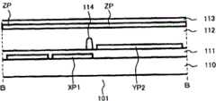
图6是在图5(A)的线A-A处所示的概略剖视图。再有,图6所示的剖视图中只示出为说明触摸屏动作所必需的层。Fig. 6 is a schematic sectional view taken along line A-A of Fig. 5(A). Note that only the layers necessary for explaining the operation of the touch panel are shown in the cross-sectional view shown in FIG. 6 .
触摸屏101的各电极形成在透明基板110上。从透明基板110开始由近及远依次说明各层。首先在靠近透明基板110的位置形成X电极XP,接着形成将X电极和Y电极绝缘的绝缘膜111。随后,形成Y电极YP。这里,也可将X电极XP和Y电极的顺序交换。在设置Y电极YP之后,设置压力检测用绝缘层112,接着设置Z电极ZP和保护层113。Each electrode of the
压力检测用绝缘层112可采用在触摸操作的按压时膜厚变化的透明绝缘材料。例如,可用弹性绝缘材料等来形成压力检测用绝缘层112。压力检测用绝缘层112适合采用空气等受压而发生体积变化的气体。在这种情况下,为了将非接触时的层间距离保持一定,也可在Z电极ZP和X电极XP及Y电极YP之间配置间隔物114等。The insulating
接着,用图7及图8说明触摸屏101中的触摸操作时的电容变化。Next, changes in capacitance during a touch operation on
图7是说明触摸操作的输入工具为手指等导体时的电容变化的示意图。这里,假定由于触摸时的按压小,压力检测用绝缘层112的厚度不变化。FIG. 7 is a schematic diagram illustrating changes in capacitance when the input tool for touch operation is a conductor such as a finger. Here, it is assumed that the thickness of the insulating
另外,各电极的电极电容成为与相邻电极之间的边缘电容、交叉电容和其他寄生电容的合成电容,但这里仅着眼于与Z电极ZP之间的平行平板电容,并假定其他的电极电容在触摸操作时和无触摸操作的情况下没有变化。这里,设无触摸操作时的Z电极ZPA与X电极XP1之间的电容为Cxz、Z电极ZPA与Y电极YP2之间的电容为Cyz。In addition, the electrode capacitance of each electrode becomes the combined capacitance of fringe capacitance, cross capacitance and other parasitic capacitances with adjacent electrodes, but here we only focus on the parallel plate capacitance with the Z electrode ZP, and assume other electrode capacitances There is no change between touch operation and no touch operation. Here, it is assumed that the capacitance between the Z electrode ZPA and the X electrode XP1 during the touchless operation is Cxz, and the capacitance between the Z electrode ZPA and the Y electrode YP2 is Cyz.
电容检测部102检测X电极XP1的电极电容时,Y电极YP2在复位状态下成为特定的基准电位。由于Z电极ZPA浮置,从X电极XP1看到的合成电容成为Cxz与Cyz串联的电容。这时的X电极的合成电容Cxp表示为:Cxp=Cxz·Cyz/(Cxz+Cyz)。When the
另一方面,在由于触摸操作而有手指接触时,可视为在Z电极ZPA上电连接了手指的静电电容分量Cf的状态。用等效电路描述这时的合成电容,则成为图7(B)所示的情况,触摸操作时的X电极的合成电容Cxpf表示为:Cxpf=Cxz·(Cyz+Cf)/(Cxz+Cyz+Cf)。On the other hand, when a finger comes into contact with the touch operation, it can be considered that the electrostatic capacitance component Cf of the finger is electrically connected to the Z electrode ZPA. Using an equivalent circuit to describe the composite capacitance at this time, it becomes the situation shown in FIG. +Cf).
控制运算部103计算出无触摸操作时的X电极XP1的电容Cxp和有触摸操作时的X电极XP1的电容Cxpf之间的差分,作为X电极XP1的信号分量。有无触摸操作时的电极电容的差分ΔCxp成为:ΔCxp=Cxz2·Cf/{(Cxz+Cyz)(Cxz+Cyz+Cf)},X电极电容的差分ΔCxp依存于手指的静电电容Cf。因此,如果通过控制运算部103对Y电极YP2施加特定电压的脉冲信号309,就可将X电极XP1的电容变化作为信号变化检测。The
图8是说明触摸操作的输入工具是例如非导电性的树脂制触笔120,压力检测用绝缘层112的厚度因触摸时的按压而变化时的电容变化的示意图。8 is a schematic diagram illustrating a change in capacitance when the input tool for touch operation is, for example, a non-conductive resin stylus 120 and the thickness of the pressure
无触摸操作时的X电极XP1的电容能够以图7所示进行说明。图8表示触摸时的按压使Z电极ZPA与X电极XP及Y电极YP(以下也将两电极称为电容检测用电极)之间的压力检测用绝缘层112变薄的状况。The capacitance of the X electrode XP1 at the time of no-touch operation can be described as shown in FIG. 7 . 8 shows how the pressure
设这时Z电极ZPA与X电极XP1间的电容为Cxza、Z电极ZPA与Y电极YP2间的电容为Cyza,则由于平行平板电容与厚度成反比例,有Cxza>Cxz、Cyza>Cyz的关系成立。Assuming that the capacitance between the Z electrode ZPA and the X electrode XP1 is Cxza, and the capacitance between the Z electrode ZPA and the Y electrode YP2 is Cyza, then since the capacitance of the parallel plate is inversely proportional to the thickness, the relationship of Cxza>Cxz and Cyza>Cyz holds true .
电容检测部102检测X电极XP1的电极电容时,Y电极YP2在复位状态下成为特定的基准电位。因此,由于Z电极ZPA浮置,从X电极XP1看到的合成电容为Cxza与Cyza串联的电容。这时的X电极的合成电容Cxpa表示为:Cxpa=Cxza·Cyza/(Cxza+Cyza)。When the
控制运算部103算出无触摸操作时的X电极XP1的电容Cxp与有触摸操作时的X电极XP1的电容Cxpa之间的差分,作为X电极XP1的信号分量。触摸操作有无时电容的差分ΔCxpa表示为:ΔCxpa={Cxz·Cxza(Cyza-Cyz)+Cyz·Cyza(Cxza-Cxz)}/{(Cxz+Cyz)(Cxza+Cyza)}。The
如果在Y电极YP2上施加特定电压的脉冲信号309,电容检测部102就可将X电极XP1的电容的差分Δcxpa作为信号变化检测。When the
以上,通过使用压力检测用绝缘层112和Z电极ZP,即便是非导电性的输入工具,也可通过按压导致的压力检测用绝缘层112的厚度变化,利用电容变化检测输入坐标。As described above, by using the pressure
接着,用图9说明在触摸操作的接触面小的情况下,接触面的位置在横向变化时各电极的信号分量。Next, the signal components of the respective electrodes when the position of the touch surface changes laterally when the touch surface is small in the touch operation will be described with reference to FIG. 9 .
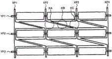
图9表示在相邻的2个X电极即XP2和XP3之间,接触面的位置在X电极上变化的状态。XA是X电极XP2的中心附近、XB是X电极XP2和XP3的中间附近、XC是X电极XP3的中心附近。图9中,为了简化未示出Z电极ZP。FIG. 9 shows a state where the position of the contact surface changes on the X electrodes between two adjacent X electrodes, XP2 and XP3. XA is near the center of X electrode XP2, XB is near the middle of X electrodes XP2 and XP3, and XC is near the center of X electrode XP3. In FIG. 9 , the Z electrode ZP is not shown for simplicity.
图7描述的静电电容Cf或图8描述的Z电极ZP与电容检测用电极之间的电容变化均依存于接触面的面积。因此,如果电容检测用电极与接触面的重叠面积大,信号分量就变大,相反地,如果电容检测用电极与接触面的重叠面积小,信号分量就变小。Both the capacitance Cf shown in FIG. 7 and the capacitance change between the Z electrode ZP and the capacitance detection electrode shown in FIG. 8 depend on the area of the contact surface. Therefore, if the overlapping area of the capacitance detecting electrode and the contact surface is large, the signal component becomes large, and conversely, if the overlapping area of the capacitance detecting electrode and the contact surface is small, the signal component becomes small.
在位置XA,接触面与X电极XP2的重叠部分多,而与X电极XP3之间几乎不重叠,因此,X电极XP2的信号分量大而X电极XP3的信号分量小。在位置XB上,X电极XP2和XP3与接触面的重叠面积大致相等,因此算出的信号分量在X电极XP2和XP3上大致相等。并且,在位置XC处,接触面与X电极XP3的重叠部分多,而与X电极XP2几乎不重叠,因此,X电极XP3的信号分量大而X电极XP2的信号分量小。控制计算部103用各电极的信号分量进行重心计算,算出通过触摸操作对接触面进行接触的输入坐标。At position XA, the contact surface overlaps a lot with X electrode XP2 and hardly overlaps with X electrode XP3, so the signal component of X electrode XP2 is large and the signal component of X electrode XP3 is small. At the position XB, the overlapping areas of the X electrodes XP2 and XP3 with the contact surface are approximately equal, and thus the calculated signal components are approximately equal at the X electrodes XP2 and XP3. In addition, at position XC, the contact surface overlaps a lot with X electrode XP3 and hardly overlaps with X electrode XP2, so the signal component of X electrode XP3 is large and the signal component of X electrode XP2 is small. The
如位置XB那样,如果在X电极XP2与XP3上获得同等的信号分量,则重心位置来到X电极XP2与XP3的中间,因此可算出输入坐标。另一方面,如位置XA或XB那样,如果一方的X电极的信号分量很大,则重心位置在检测大信号分量的X电极附近,因此,同样可算出输入坐标。As in the position XB, if the same signal components are obtained on the X electrodes XP2 and XP3, the center of gravity will be in the middle of the X electrodes XP2 and XP3, so the input coordinates can be calculated. On the other hand, if the signal component of one of the X electrodes is large as in position XA or XB, the center of gravity is near the X electrode that detects the large signal component, and thus the input coordinates can be calculated similarly.
如上所述,通过将X电极的电极形状设为朝相邻的电极收窄的形状,即便在与接触面相比X电极的电极间隔宽的情况下,也能来进行重心计算,以高精度地检测位置。因此,通过与接触面相比来扩大X电极的电极间隔,从而与以往的电极图案相比,可以减少电极条数。另外,尽管将Y电极夹于其间的X电极的电极形状是离散的,但通过将电气上浮置的Z电极ZP配置成跨越相邻的X电极XP和Y电极YP,能够在整个触摸屏上检测X方向的输入坐标。As described above, by making the electrode shape of the X electrode narrow toward the adjacent electrode, even when the electrode interval of the X electrode is wider than that of the contact surface, it is possible to calculate the center of gravity with high accuracy. Detect location. Therefore, by increasing the electrode interval of the X electrodes compared to the contact surface, the number of electrodes can be reduced compared to conventional electrode patterns. In addition, although the electrode shape of the X electrode sandwiching the Y electrode is discrete, by disposing the electrically floating Z electrode ZP to straddle the adjacent X electrode XP and Y electrode YP, it is possible to detect the X electrode on the entire touch screen. The input coordinates for the direction.
图10表示将图5(B)所示的X电极XP的形状改变后的状况。图5(B)和图10中,Y电极YP的形状相同。图5(B)中X电极XP形状朝左右两侧呈凸出形状,而在图10中,如X电极XP2那样,朝相邻的一方的X电极XP1呈凸出形状,并朝相邻的另一方的X电极XP3呈凹入形状。FIG. 10 shows a state in which the shape of the X electrode XP shown in FIG. 5(B) is changed. In FIG. 5(B) and FIG. 10 , the shape of the Y electrode YP is the same. In FIG. 5(B), the shape of the X electrode XP is convex toward the left and right sides. In FIG. The other X electrode XP3 has a concave shape.
图5(B)和图10的共同特征在于,面积随着与相邻的X电极XP的中心接近而减小,且越接近该X电极XP的中心其面积变得越大。因此,图10所示的X电极XP也可望取得与图5(B)相同的效果。再有,电极形状并不限于图5(B)、图10的形状,只要X电极的形状随着与相邻的X电极的中心接近而面积减小且越接近该X电极的中心面积越大的形状就可以。The common feature of FIG. 5(B) and FIG. 10 is that the area decreases as the center of the adjacent X electrode XP approaches, and the area becomes larger as it approaches the center of the X electrode XP. Therefore, the X electrode XP shown in FIG. 10 can also be expected to achieve the same effect as that of FIG. 5(B). Furthermore, the shape of the electrode is not limited to the shape of Fig. 5(B) and Fig. 10, as long as the shape of the X electrode is close to the center of the adjacent X electrode, the area decreases and the closer to the center of the X electrode, the larger the area The shape will do.
接着,用图11表示Z电极ZP上不形成狭缝的触摸屏。图11(B)是在图11(A)的B-B线处剖切的概略剖视图。图11所示的Z电极ZP未被狭缝分割,具有无狭缝电极(solid elctrode,未设置间隔或间隙的连续形状的电极)的形状。该无狭缝电极形状的Z电极ZP也设为电气浮置状态。无狭缝电极形状的Z电极ZP夹着压力检测用绝缘层112而配置在X电极XP和Y电极YP的上部。Next, a touch panel in which no slit is formed on the Z electrode ZP is shown in FIG. 11 . Fig. 11(B) is a schematic sectional view taken along line B-B in Fig. 11(A). The Z electrode ZP shown in FIG. 11 is not divided by a slit, and has a shape without a slit electrode (solid electrode (a continuous shape electrode without intervals or gaps). The Z electrode ZP of this slit-free electrode shape is also in an electrically floating state. The Z electrode ZP of the electrode shape without a slit is arranged on the upper part of the X electrode XP and the Y electrode YP with the pressure
尽管采用无狭缝电极形状的Z电极ZP,也能跟使用有狭缝Z电极ZP时相同程度地将基于压力检测用绝缘层112的层间距离变化的电容变化作为信号分量检测。并且已知,用手指等轻微接触时,在接触时压力检测用绝缘层112的层间距离无变化,但能通过提高Z电极的薄膜电阻来获得与使用有狭缝Z电极ZP时同等程度的信号分量。通过提高Z电极的薄膜电阻,使得只是与所接触的导体的距离近的电容检测用电极能够对由该所接触的导体发生的静电电容进行充放电。如此,通过提高Z电极的电阻来局部地对静电电容充放电,从而能够检测信号分量。Even if the Z electrode ZP having an electrode shape without a slit is used, the change in capacitance due to the change in the interlayer distance of the pressure
图12是触摸屏101的截面结构的说明图。沿图12(A)所示的Xa-Xb线段、Ya-Yb线段剖切的截面示出了结构中的保护层113与透明基板110的距离关系。图12(B)表示沿上述Xa-Xb线段剖切的截面结构。保护层113经由连接部1205与透明基板110连接。这里连接部1205附近的保护层113与透明基板110的距离1201、跟Xa-Xb线段中点附近的保护层113与透明基板110的距离1202的关系,满足距离1201<距离1202。FIG. 12 is an explanatory diagram of a cross-sectional structure of the
另外,图12(C)表示沿上述Ya-Yb线段剖切的截面结构。同样,保护层113经由连接部1205与透明基板110连接。这里,连接部1205附近的保护层113与透明基板110的距离1203、跟Ya-Yb线段中点附近的保护层113与透明基板110的距离1204的关系,满足距离1203<距离1204。In addition, FIG. 12(C) shows a cross-sectional structure cut along the line segment Ya-Yb. Likewise, the
如果满足上述关系中的至少任何一方,则成为向保护层113的上方向回弹力加强的结构,因此,可促使在分离对触摸屏101的接触时保护层113形状的恢复,加快响应速度。If at least one of the above-mentioned relationships is satisfied, it becomes a structure with stronger resilience toward the upper side of the
如以上说明,根据本实施例,即使利用非导电性的输入工具接触到触摸屏上,也可通过电容检测用的X电极XP或Y电极YP跟其上部的Z电极ZP的距离变化来使电容发生变化,能够以静电电容耦合方式检测输入坐标。从而,使导电性低的树脂制触笔也能适用。As described above, according to this embodiment, even if a non-conductive input tool is used to touch the touch screen, capacitance can be generated by changing the distance between the X electrode XP or Y electrode YP for capacitance detection and the upper Z electrode ZP. Changes, the input coordinates can be detected by electrostatic capacitive coupling. Therefore, a stylus made of resin with low conductivity can also be applied.
另外,通过在电极形状上设法改进,以使相邻X电极间的输入位置可根据从相邻的2个X电极得到的电容变化的信号比算出,从而可减少X电极条数,并可通过在Z电极的配置上设法改进来减少Y电极。从而,能够减小从检测用电极到输入处理部引绕布线所需的边框宽度,提高设计上的可能性。另外,由于能够限制输入处理部的端子数增加,能够低成本地实现可进行高精度输入位置检测的静电电容耦合方式的触摸屏。此外,由于用接触面小的输入工具例如触笔等也能高精度地检测输入坐标,所以也可适用于文字输入等的应用。In addition, by trying to improve the electrode shape, the input position between adjacent X electrodes can be calculated according to the signal ratio of the capacitance change obtained from two adjacent X electrodes, so that the number of X electrodes can be reduced, and through Try to improve the configuration of the Z electrodes to reduce the Y electrodes. Therefore, it is possible to reduce the frame width required to route the wiring from the detection electrode to the input processing unit, thereby improving design possibilities. In addition, since the increase in the number of terminals of the input processing unit can be limited, a capacitive coupling type touch panel capable of high-precision input position detection can be realized at low cost. In addition, since input coordinates can be detected with high precision even with an input tool with a small contact surface such as a stylus, it is also suitable for applications such as character input.
另外,对X电极XP或Y电极YP中任何一方依次施加脉冲信号,预先判别是来自哪个电极的信号,即使在接触2点的情况下也能高精度地进行检测。In addition, pulse signals are sequentially applied to either the X electrode XP or the Y electrode YP, and it is judged in advance which electrode the signal comes from, so that even when two points are in contact, it is possible to detect with high precision.
以上,基于上述实施例对本发明人提出的发明作了具体说明,不言而喻,本发明并不限定于上述实施例,在不脱离其要点的范围内可能有各种变更。As mentioned above, the invention proposed by this inventor was concretely demonstrated based on the said Example, It goes without saying that this invention is not limited to the said Example, Various changes are possible in the range which does not deviate from the summary.
Claims (16)
Translated fromChineseApplications Claiming Priority (2)
| Application Number | Priority Date | Filing Date | Title |
|---|---|---|---|
| JP2008300678AJP5491020B2 (en) | 2008-11-26 | 2008-11-26 | Touch panel |
| JP2008-300678 | 2008-11-26 |
Publications (2)
| Publication Number | Publication Date |
|---|---|
| CN101901090A CN101901090A (en) | 2010-12-01 |
| CN101901090Btrue CN101901090B (en) | 2013-10-16 |
Family
ID=42222389
Family Applications (1)
| Application Number | Title | Priority Date | Filing Date |
|---|---|---|---|
| CN2009102249963AActiveCN101901090B (en) | 2008-11-26 | 2009-11-26 | Display device |
Country Status (5)
| Country | Link |
|---|---|
| US (1) | US8487901B2 (en) |
| JP (1) | JP5491020B2 (en) |
| KR (1) | KR101122875B1 (en) |
| CN (1) | CN101901090B (en) |
| TW (1) | TWI433014B (en) |
Families Citing this family (35)
| Publication number | Priority date | Publication date | Assignee | Title |
|---|---|---|---|---|
| JP5100738B2 (en)* | 2009-04-22 | 2012-12-19 | 株式会社ジャパンディスプレイイースト | Input device and display device including the same |
| US20100271328A1 (en)* | 2009-04-22 | 2010-10-28 | Shinji Sekiguchi | Input device and display device having the same |
| US9383881B2 (en) | 2009-06-03 | 2016-07-05 | Synaptics Incorporated | Input device and method with pressure-sensitive layer |
| JP5295914B2 (en)* | 2009-09-18 | 2013-09-18 | 株式会社ジャパンディスプレイ | Display device |
| TWI397843B (en)* | 2009-10-30 | 2013-06-01 | Orise Technology Co Ltd | Touch panel sensing circuit |
| TWI417778B (en)* | 2010-02-26 | 2013-12-01 | Raydium Semiconductor Corp | Capacitance offset compensation for electronic device |
| US8717312B2 (en)* | 2010-07-26 | 2014-05-06 | Au Optronics Corporation | Touch sensing device |
| JP5606242B2 (en)* | 2010-09-24 | 2014-10-15 | 株式会社ジャパンディスプレイ | Display device |
| JP5563417B2 (en)* | 2010-09-30 | 2014-07-30 | 株式会社ジャパンディスプレイ | Display device with touch panel |
| JP5496851B2 (en)* | 2010-10-22 | 2014-05-21 | 株式会社ジャパンディスプレイ | Touch panel |
| JP5797973B2 (en)* | 2011-02-08 | 2015-10-21 | ローム株式会社 | CAPACITANCE / VOLTAGE CONVERSION CIRCUIT, INPUT DEVICE USING SAME, ELECTRONIC DEVICE, AND CAPACITANCE / VOLTAGE CONVERSION METHOD |
| JP5823729B2 (en)* | 2011-05-09 | 2015-11-25 | シナプティクス・ディスプレイ・デバイス合同会社 | Semiconductor device and data processing system |
| JP5777094B2 (en)* | 2011-07-14 | 2015-09-09 | 株式会社ワコム | Position detection sensor and position detection device |
| US8698769B2 (en)* | 2011-08-01 | 2014-04-15 | Sharp Kabushiki Kaisha | Dual mode capacitive touch panel |
| KR101369431B1 (en)* | 2011-11-30 | 2014-03-06 | 주식회사 팬택 | touch panel, apparatus for sensing touch including touch panel and method for sensing touch |
| KR101940759B1 (en)* | 2011-12-23 | 2019-01-21 | 엘지디스플레이 주식회사 | Driving method of touch screen and liquid crystal display device including the touch screen |
| CN103309488B (en)* | 2012-03-15 | 2016-08-24 | 宸鸿科技(厦门)有限公司 | Contact panel and manufacture method thereof |
| KR20140087695A (en)* | 2012-12-31 | 2014-07-09 | 삼성디스플레이 주식회사 | Display device including sensing unit and driving method thereof |
| KR101537231B1 (en)* | 2013-06-27 | 2015-07-16 | 크루셜텍 (주) | Touch detecting apparatus and method |
| KR102245943B1 (en)* | 2014-06-23 | 2021-04-29 | 엘지디스플레이 주식회사 | Touch panel and apparatus for driving thereof |
| KR102384103B1 (en)* | 2014-08-26 | 2022-04-07 | 엘지디스플레이 주식회사 | Apparatus for driving of touch panel |
| CN106293188B (en)* | 2015-06-10 | 2023-10-24 | 宸鸿科技(厦门)有限公司 | Touch panel |
| US10175807B2 (en) | 2015-12-18 | 2019-01-08 | Stmicroelectronics Asia Pacific Pte Ltd | Support of narrow tip styluses on touch screen devices |
| KR101809917B1 (en)* | 2016-01-29 | 2017-12-21 | 엘지디스플레이 주식회사 | Driving circuit, touch display device, and method for driving the touch display device |
| TWI604355B (en) | 2016-06-17 | 2017-11-01 | 速博思股份有限公司 | Sensing apparatus for touch and force sensing |
| TWI633469B (en)* | 2016-08-12 | 2018-08-21 | 鴻海精密工業股份有限公司 | On-cell touch display apparatus |
| US10481723B2 (en)* | 2016-10-28 | 2019-11-19 | Stmicroelectronics Asia Pacific Pte Ltd | Hover rejection through dynamic thresholding |
| CN106547378A (en)* | 2016-12-07 | 2017-03-29 | 歌尔科技有限公司 | A kind of contactor control device and virtual reality system for VR equipment |
| TWI622911B (en)* | 2017-02-14 | 2018-05-01 | 宏碁股份有限公司 | Touch device |
| KR20180099230A (en)* | 2017-02-28 | 2018-09-05 | 동우 화인켐 주식회사 | Digitizer and Method of Preparing the Same |
| TWI664567B (en)* | 2018-06-12 | 2019-07-01 | 友達光電股份有限公司 | Touch device and method of driving touch device |
| JP7106402B2 (en)* | 2018-09-11 | 2022-07-26 | 株式会社ジャパンディスプレイ | Display device |
| TWI710940B (en)* | 2018-12-17 | 2020-11-21 | 日商阿爾卑斯阿爾派股份有限公司 | Input device |
| US11703983B2 (en)* | 2020-03-25 | 2023-07-18 | Sensortek Technology Corp | Capacitance sensing circuit |
| CN112328114B (en)* | 2020-11-13 | 2022-12-23 | 深圳天德钰科技股份有限公司 | Positioning method and positioning device for touch position and touch display device |
Citations (2)
| Publication number | Priority date | Publication date | Assignee | Title |
|---|---|---|---|---|
| CN1758198A (en)* | 2004-10-07 | 2006-04-12 | 阿尔卑斯电气株式会社 | Capacitive coordinate detection device |
| CN1987761A (en)* | 2005-12-19 | 2007-06-27 | 阿尔卑斯电气株式会社 | Input device |
Family Cites Families (13)
| Publication number | Priority date | Publication date | Assignee | Title |
|---|---|---|---|---|
| US4087625A (en)* | 1976-12-29 | 1978-05-02 | International Business Machines Corporation | Capacitive two dimensional tablet with single conductive layer |
| JPS5923410B2 (en)* | 1978-06-09 | 1984-06-01 | パナフアコム株式会社 | tatsuchi keyboard |
| US5113041A (en)* | 1990-12-28 | 1992-05-12 | At&T Bell Laboratories | Information processing |
| AU5697794A (en)* | 1992-12-11 | 1994-07-04 | Signagraphics Corporation (Inc.) | Data input device with a pressure-sensitive input surface |
| JPH0996792A (en)* | 1995-09-29 | 1997-04-08 | Optrex Corp | Liquid crystal display element with input function |
| JP3277896B2 (en)* | 1998-07-31 | 2002-04-22 | ぺんてる株式会社 | Capacitance coordinate detection device that also serves as pressure detection |
| JP4441368B2 (en)* | 2004-09-28 | 2010-03-31 | 日立プラズマディスプレイ株式会社 | Plasma display panel driving method and plasma display apparatus |
| KR100749464B1 (en)* | 2005-09-29 | 2007-08-14 | 삼성에스디아이 주식회사 | Plasma display panel |
| DE202007005237U1 (en)* | 2006-04-25 | 2007-07-05 | Philipp, Harald, Southampton | Touch-sensitive position sensor for use in control panel, has bus bars arranged at distance to substrate, and detection region with units that are arranged at distance by non-conductive openings such that current flows into region |
| GB2437827B (en)* | 2006-05-05 | 2008-03-26 | Harald Philipp | Touch screen element |
| KR20090100639A (en)* | 2008-03-20 | 2009-09-24 | 삼성전자주식회사 | Display panel and manufacturing method thereof |
| JP5345336B2 (en) | 2008-04-15 | 2013-11-20 | 株式会社ジャパンディスプレイ | Input device and display device including the same |
| JP5123774B2 (en) | 2008-07-25 | 2013-01-23 | 株式会社ジャパンディスプレイイースト | Input device and display device including the same |
- 2008
- 2008-11-26JPJP2008300678Apatent/JP5491020B2/enactiveActive
- 2009
- 2009-11-13TWTW098138709Apatent/TWI433014B/enactive
- 2009-11-24USUS12/624,434patent/US8487901B2/ennot_activeExpired - Fee Related
- 2009-11-25KRKR1020090114427Apatent/KR101122875B1/enactiveActive
- 2009-11-26CNCN2009102249963Apatent/CN101901090B/enactiveActive
Patent Citations (2)
| Publication number | Priority date | Publication date | Assignee | Title |
|---|---|---|---|---|
| CN1758198A (en)* | 2004-10-07 | 2006-04-12 | 阿尔卑斯电气株式会社 | Capacitive coordinate detection device |
| CN1987761A (en)* | 2005-12-19 | 2007-06-27 | 阿尔卑斯电气株式会社 | Input device |
Also Published As
| Publication number | Publication date |
|---|---|
| TW201032116A (en) | 2010-09-01 |
| KR20100059714A (en) | 2010-06-04 |
| US8487901B2 (en) | 2013-07-16 |
| TWI433014B (en) | 2014-04-01 |
| CN101901090A (en) | 2010-12-01 |
| US20100134440A1 (en) | 2010-06-03 |
| JP2010128647A (en) | 2010-06-10 |
| KR101122875B1 (en) | 2012-03-20 |
| JP5491020B2 (en) | 2014-05-14 |
Similar Documents
| Publication | Publication Date | Title |
|---|---|---|
| CN101901090B (en) | Display device | |
| US9684409B2 (en) | Hover position calculation in a touchscreen device | |
| JP5345336B2 (en) | Input device and display device including the same | |
| KR101240065B1 (en) | Display device | |
| US8115744B2 (en) | Multi-point touch-sensitive system | |
| US9983738B2 (en) | Contact detection mode switching in a touchscreen device | |
| CN102880364B (en) | A capacitive touch screen system and method for collecting charges in the system | |
| US20090314551A1 (en) | Touch panel | |
| CN101414236A (en) | On-screen input image display system | |
| TW201145134A (en) | Capacitance sensor and information input apparatus | |
| US20160005352A1 (en) | Touch sensing device | |
| KR102139424B1 (en) | Capacitive input device | |
| CN104077000B (en) | Touch panel and its driving method, display device | |
| KR20090076125A (en) | Method of calculating touch coordinate of touch screen and device using same | |
| US8325152B2 (en) | Touch panel with unbalanced conductive patterns, and touch-controlled apparatus and method for determining multi-touch thereof | |
| US20150324044A1 (en) | Capacitive touch sensor architecture with adjustable resistance and noise reduction method | |
| US10303319B2 (en) | Pattern of Electrodes for a touch sensor | |
| CN113056721A (en) | Input device | |
| WO2023053488A1 (en) | Electrostatic capacitance sensor | |
| TWI460646B (en) | Resistive touch panel | |
| KR101094623B1 (en) | Display device | |
| TWI470528B (en) | Resistive touch panel | |
| KR20130099498A (en) | Single layer capacitive multi touch screen apparatus |
Legal Events
| Date | Code | Title | Description |
|---|---|---|---|
| C06 | Publication | ||
| PB01 | Publication | ||
| C10 | Entry into substantive examination | ||
| SE01 | Entry into force of request for substantive examination | ||
| ASS | Succession or assignment of patent right | Owner name:PANASONIC LCD CO., LTD. Free format text:FORMER OWNER: IPS ALPHA SUPPORT CO., LTD. Effective date:20111129 Owner name:IPS ALPHA SUPPORT CO., LTD. Effective date:20111129 | |
| C41 | Transfer of patent application or patent right or utility model | ||
| TA01 | Transfer of patent application right | Effective date of registration:20111129 Address after:Chiba County, Japan Applicant after:Hitachi Displays, Ltd. Co-applicant after:Panasonic Liquid Crystal Display Co.,Ltd. Address before:Chiba County, Japan Applicant before:Hitachi Displays, Ltd. Co-applicant before:IPS pioneer support society Effective date of registration:20111129 Address after:Chiba County, Japan Applicant after:Hitachi Displays, Ltd. Co-applicant after:IPS Pioneer Support Society Address before:Chiba County, Japan Applicant before:Hitachi Displays, Ltd. | |
| C14 | Grant of patent or utility model | ||
| GR01 | Patent grant | ||
| CP01 | Change in the name or title of a patent holder | ||
| CP01 | Change in the name or title of a patent holder | Address after:Chiba County, Japan Patentee after:Japan Display East Inc. Patentee after:Panasonic Liquid Crystal Display Co.,Ltd. Address before:Chiba County, Japan Patentee before:Hitachi Displays, Ltd. Patentee before:Panasonic Liquid Crystal Display Co.,Ltd. | |
| CP03 | Change of name, title or address | ||
| CP03 | Change of name, title or address | Address after:Tokyo, Japan Patentee after:JAPAN DISPLAY Inc. Patentee after:Panasonic Liquid Crystal Display Co.,Ltd. Address before:Chiba County, Japan Patentee before:Japan Display East Inc. Patentee before:Panasonic Liquid Crystal Display Co.,Ltd. | |
| TR01 | Transfer of patent right | ||
| TR01 | Transfer of patent right | Effective date of registration:20231013 Address after:Tokyo, Japan Patentee after:JAPAN DISPLAY Inc. Patentee after:PANASONIC INTELLECTUAL PROPERTY CORPORATION OF AMERICA Address before:Tokyo, Japan Patentee before:JAPAN DISPLAY Inc. Patentee before:Panasonic Liquid Crystal Display Co.,Ltd. | |
| TR01 | Transfer of patent right | ||
| TR01 | Transfer of patent right | Effective date of registration:20240909 Address after:6600 Chase Oaks Avenue, Unit 150, Plano, Texas, USA Patentee after:Touch Panel Technology Co.,Ltd. Country or region after:U.S.A. Address before:Tokyo, Japan Patentee before:JAPAN DISPLAY Inc. Country or region before:Japan Patentee before:PANASONIC INTELLECTUAL PROPERTY CORPORATION OF AMERICA Country or region before:U.S.A. |