CN101894807A - TFT-LCD (Thin Film Transistor-Liquid Crystal Display) array base plate and manufacturing method thereof - Google Patents
TFT-LCD (Thin Film Transistor-Liquid Crystal Display) array base plate and manufacturing method thereofDownload PDFInfo
- Publication number
- CN101894807A CN101894807ACN2009100855066ACN200910085506ACN101894807ACN 101894807 ACN101894807 ACN 101894807ACN 2009100855066 ACN2009100855066 ACN 2009100855066ACN 200910085506 ACN200910085506 ACN 200910085506ACN 101894807 ACN101894807 ACN 101894807A
- Authority
- CN
- China
- Prior art keywords
- tft
- photoresist
- film
- source
- manufacturing
- Prior art date
- Legal status (The legal status is an assumption and is not a legal conclusion. Google has not performed a legal analysis and makes no representation as to the accuracy of the status listed.)
- Granted
Links
- 238000004519manufacturing processMethods0.000titleclaimsabstractdescription37
- 239000010409thin filmSubstances0.000titleclaimsabstractdescription27
- 239000004973liquid crystal related substanceSubstances0.000titleabstractdescription4
- 239000004065semiconductorSubstances0.000claimsabstractdescription55
- 238000000034methodMethods0.000claimsabstractdescription48
- 239000000203mixtureSubstances0.000claimsabstractdescription31
- 238000000151depositionMethods0.000claimsabstractdescription20
- 229910052751metalInorganic materials0.000claimsabstractdescription19
- 239000002184metalSubstances0.000claimsabstractdescription19
- 230000008569processEffects0.000claimsabstractdescription16
- 239000010408filmSubstances0.000claimsdescription90
- 229920002120photoresistant polymerPolymers0.000claimsdescription70
- 239000010410layerSubstances0.000claimsdescription50
- 238000005530etchingMethods0.000claimsdescription30
- 239000000758substrateSubstances0.000claimsdescription21
- 230000008021depositionEffects0.000claimsdescription15
- 238000004380ashingMethods0.000claimsdescription7
- 239000011248coating agentSubstances0.000claimsdescription5
- 238000000576coating methodMethods0.000claimsdescription5
- 229910052750molybdenumInorganic materials0.000claimsdescription5
- NBIIXXVUZAFLBC-UHFFFAOYSA-NPhosphoric acidChemical compoundOP(O)(O)=ONBIIXXVUZAFLBC-UHFFFAOYSA-N0.000claimsdescription4
- QAOWNCQODCNURD-UHFFFAOYSA-NSulfuric acidChemical compoundOS(O)(=O)=OQAOWNCQODCNURD-UHFFFAOYSA-N0.000claimsdescription4
- VYZAMTAEIAYCRO-UHFFFAOYSA-NChromiumChemical compound[Cr]VYZAMTAEIAYCRO-UHFFFAOYSA-N0.000claimsdescription3
- RYGMFSIKBFXOCR-UHFFFAOYSA-NCopperChemical compound[Cu]RYGMFSIKBFXOCR-UHFFFAOYSA-N0.000claimsdescription3
- ZOKXTWBITQBERF-UHFFFAOYSA-NMolybdenumChemical compound[Mo]ZOKXTWBITQBERF-UHFFFAOYSA-N0.000claimsdescription3
- 229910000583Nd alloyInorganic materials0.000claimsdescription3
- VYPSYNLAJGMNEJ-UHFFFAOYSA-NSilicium dioxideChemical compoundO=[Si]=OVYPSYNLAJGMNEJ-UHFFFAOYSA-N0.000claimsdescription3
- 229910052782aluminiumInorganic materials0.000claimsdescription3
- XAGFODPZIPBFFR-UHFFFAOYSA-NaluminiumChemical compound[Al]XAGFODPZIPBFFR-UHFFFAOYSA-N0.000claimsdescription3
- 229910052804chromiumInorganic materials0.000claimsdescription3
- 239000011651chromiumSubstances0.000claimsdescription3
- 239000011733molybdenumSubstances0.000claimsdescription3
- WFKWXMTUELFFGS-UHFFFAOYSA-NtungstenChemical compound[W]WFKWXMTUELFFGS-UHFFFAOYSA-N0.000claimsdescription3
- 229910052721tungstenInorganic materials0.000claimsdescription3
- 239000010937tungstenSubstances0.000claimsdescription3
- GRYLNZFGIOXLOG-UHFFFAOYSA-NNitric acidChemical compoundO[N+]([O-])=OGRYLNZFGIOXLOG-UHFFFAOYSA-N0.000claimsdescription2
- 229910004205SiNXInorganic materials0.000claimsdescription2
- 229910020286SiOxNyInorganic materials0.000claimsdescription2
- 229910000147aluminium phosphateInorganic materials0.000claimsdescription2
- 239000000463materialSubstances0.000claimsdescription2
- 229910017604nitric acidInorganic materials0.000claimsdescription2
- 150000002978peroxidesChemical class0.000claimsdescription2
- 229910052814silicon oxideInorganic materials0.000claimsdescription2
- 238000000059patterningMethods0.000claims3
- 239000002356single layerSubstances0.000claims2
- UBSJOWMHLJZVDJ-UHFFFAOYSA-Naluminum neodymiumChemical compound[Al].[Nd]UBSJOWMHLJZVDJ-UHFFFAOYSA-N0.000claims1
- 229910052802copperInorganic materials0.000claims1
- 239000010949copperSubstances0.000claims1
- 238000005516engineering processMethods0.000description37
- 238000009413insulationMethods0.000description12
- 238000011161developmentMethods0.000description7
- 101100214491Solanum lycopersicum TFT3 geneProteins0.000description6
- 239000003795chemical substances by applicationSubstances0.000description4
- 238000001312dry etchingMethods0.000description4
- 238000002161passivationMethods0.000description3
- VVTQWTOTJWCYQT-UHFFFAOYSA-Nalumane;neodymiumChemical compound[AlH3].[Nd]VVTQWTOTJWCYQT-UHFFFAOYSA-N0.000description2
- 239000004411aluminiumSubstances0.000description2
- 230000008901benefitEffects0.000description2
- 230000015572biosynthetic processEffects0.000description2
- 230000009977dual effectEffects0.000description2
- 238000001755magnetron sputter depositionMethods0.000description2
- 150000002739metalsChemical class0.000description2
- 238000002207thermal evaporationMethods0.000description2
- 238000003325tomographyMethods0.000description2
- 238000012546transferMethods0.000description2
- 238000001039wet etchingMethods0.000description2
- 229910021417amorphous siliconInorganic materials0.000description1
- 230000004888barrier functionEffects0.000description1
- 230000008859changeEffects0.000description1
- 238000005229chemical vapour depositionMethods0.000description1
- 238000005202decontaminationMethods0.000description1
- 230000003588decontaminative effectEffects0.000description1
- 230000002950deficientEffects0.000description1
- 230000005684electric fieldEffects0.000description1
- 230000002708enhancing effectEffects0.000description1
- 239000011521glassSubstances0.000description1
- 230000003760hair shineEffects0.000description1
- 238000013507mappingMethods0.000description1
- 239000012528membraneSubstances0.000description1
- 238000012986modificationMethods0.000description1
- 230000004048modificationEffects0.000description1
- 238000012545processingMethods0.000description1
- 239000010453quartzSubstances0.000description1
- 230000009467reductionEffects0.000description1
Images


Classifications
- H—ELECTRICITY
- H10—SEMICONDUCTOR DEVICES; ELECTRIC SOLID-STATE DEVICES NOT OTHERWISE PROVIDED FOR
- H10D—INORGANIC ELECTRIC SEMICONDUCTOR DEVICES
- H10D86/00—Integrated devices formed in or on insulating or conducting substrates, e.g. formed in silicon-on-insulator [SOI] substrates or on stainless steel or glass substrates
- H10D86/01—Manufacture or treatment
- H10D86/021—Manufacture or treatment of multiple TFTs
- H10D86/0231—Manufacture or treatment of multiple TFTs using masks, e.g. half-tone masks
- H—ELECTRICITY
- H10—SEMICONDUCTOR DEVICES; ELECTRIC SOLID-STATE DEVICES NOT OTHERWISE PROVIDED FOR
- H10D—INORGANIC ELECTRIC SEMICONDUCTOR DEVICES
- H10D86/00—Integrated devices formed in or on insulating or conducting substrates, e.g. formed in silicon-on-insulator [SOI] substrates or on stainless steel or glass substrates
- H10D86/40—Integrated devices formed in or on insulating or conducting substrates, e.g. formed in silicon-on-insulator [SOI] substrates or on stainless steel or glass substrates characterised by multiple TFTs
- H10D86/60—Integrated devices formed in or on insulating or conducting substrates, e.g. formed in silicon-on-insulator [SOI] substrates or on stainless steel or glass substrates characterised by multiple TFTs wherein the TFTs are in active matrices
Landscapes
- Liquid Crystal (AREA)
- Thin Film Transistor (AREA)
Abstract
Description
Technical field
The present invention relates to a kind of LCD and manufacture method thereof, especially a kind of TFT-LCD array base palte and manufacture method thereof.
Background technology
Thin-film transistor LCD device (Thin Film Transistor Liquid Crystal Display is called for short TFT-LCD) is a kind of main panel display apparatus (Flat Panel Display abbreviates FPD as).
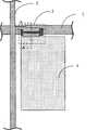
Fig. 1 is the floor map of existing TFT-LCD array base palte.As shown in Figure 1, existing array base palte (Array Substrate) comprising:grid line 1,data wire 2, thin-film transistor (Thin FirmTransistor abbreviates TFT as) 3 and pixel electrode 4.Grid line 1 is horizontally installed on thetransparency carrier 11, anddata wire 2 vertically is arranged on thetransparency carrier 11, andgrid line 1 is provided with TFT3 with the infall of data wire 2.TFT3 is the active switch element.
Fig. 2 is that the A-A of Fig. 1 is to profile.As shown in Figure 2, existing array base palte comprises:gate electrode 12,gate insulation layer 13,semiconductor layer 14,doping semiconductor layer 15,source electrode 16,drain electrode 17, passivation layer 18.Said structure all is arranged on the transparency carrier 11.Gate electrode 12 is one-body molded withgrid line 1, andsource electrode 16 is one-body molded withdata wire 2, anddrain electrode 17 generally is connected by passivation layer via hole (via hole) with pixel electrode 4.When importing Continuity signal in thegrid line 1, active layer (semiconductor layer 14 and doping semiconductor layer 15) conduction, the data-signal ofdata wire 2 can arrivedrain electrodes 17 through TFT raceway groove (channel) 19 fromsource electrode 16, finally input to pixel electrode 4.Pixel electrode 4 obtains behind the signal being formed for driving the electric field that liquid crystal rotates with public electrode (different according to the TFT-LCD type, can be arranged on the array base palte or on the color membrane substrates, not shown).
At present, the TFT-LCD array base palte is to form structure graph by composition technology repeatedly to finish, technology such as comprise mask exposure, development, etching each time in the composition technology again respectively and peel off, wherein etching technics comprises dry etching and wet etching, so the number of times of composition technology can be weighed the complicated and simple degree of making the TFT-LCD array base palte, the number of times that reduces composition technology just means the reduction of manufacturing cost.Five composition technologies of prior art comprise: grid line and gate electrode composition, active layer composition, source electrode/drain electrode composition, via hole composition and pixel electrode composition.
Disclose in a large number in the prior art, reduce manufacturing cost by reducing composition technology number of times, and the technical literature of enhancing productivity by the simplification of technology.Wherein, comparatively leading technology is: by the method for three composition technology manufacturing TFT-LCD array base paltes.This method comprises:
Step 1: deposit first metallic film, form the figure of grid line, gate electrode with normal masks plate (mask);
Step 2: deposit first insulation film, semiconductive thin film, doped semiconductor films and second metallic film successively, with first pair of figure of transferring mask plate (dual tone mask) to form TFT raceway groove, source electrode, drain electrode and data wire;
Step 3: deposit second insulation film, transfer mask plate to form via hole with second pair, residual photoresist is carried out ashing, and deposit transparent conductive layer, by liftoff peeling off (lift off) technology, with forming the pixel electrode figure after the photoresist one logical transparency conducting layer that peels off on the residual photoresist.
Deposit transparent conductive layer and the first metal layer successively instep 1, and adopt the 3rd pair to transfer mask plate, form grid line, gate electrode and common pattern of electrodes, be able on array base palte, form the figure of public electrode.
The key of above-mentionedstep 3 is, during the deposit transparent conductive layer, forms tomography in the marginal portion that forms pattern of pixel electrodes, makes follow-up liftoff stripping technology to implement, and is easy to implement.Normally when etching (etch) passivation layer, photoresist (Photo resist abbreviates PR as) is formed undercut (under cut), so-called undercut is exactly intilted hypotenuse.After forming undercut, the transparency conducting layer that is deposited in the undercut can form tomography in undercut place, the undercut of exposing photoresist, at this moment just can be from undercut with photoresist lift off, an and logical transparency conducting layer that peels off above the photoresist, and obtaining the pixel electrode figure, this method is referred to as liftoff stripping technology.
But, owing to after the undercut of etching second insulating barrier formation photoresist, also need to carry out ashing (ashing) technology of photoresist, so in the actual production, be difficult to keep photoresist and form undercut.And the different problem of degree that undercut forms can take place, i.e. the intilted degree difference of undercut, and bad probability height takes place, the problem that causes yields to reduce when causing carrying out liftoff stripping technology.In addition, can pollute transparency conducting layer during photoresist ashing, bring high fraction defective, also bring this corresponding loaded down with trivial details handling procedure.
Summary of the invention
The purpose of this invention is to provide a kind of TFT-LCD array base palte and manufacture method thereof, can be under the prerequisite that does not adopt liftoff stripping technology, only by 3 composition technology manufacturing array substrates.
Another object of the present invention provides a kind of TFT-LCD array base palte and manufacture method thereof, can avoid the cineration technics of photoresist to pollute transparency conducting layer, reduces the loaded down with trivial details handling procedure of decontamination, improves yield of products then.
For achieving the above object, the invention provides a kind of manufacture method of TFT-LCD array base palte, described array base palte comprises gate electrode zone, data wire zone, semiconductor layer zone, source electrode zone, drain electrode zone, grid region and pixel electrode area, and manufacture method comprises:
Step 1: metallic film and doped semiconductor films are leaked in deposit transparent conductive film, source successively on transparency carrier, form by the first composition technology to comprise doping semiconductor layer, source electrode, drain electrode, data wire and pattern of pixel electrodes;
Step 2: the deposited semiconductor film forms the figure that comprises TFT raceway groove and semiconductor layer by the second composition technology;
Step 3: deposition insulation film and grid metallic film form the figure that comprises grid line and gate electrode by the 3rd composition technology.
For achieving the above object, the present invention also provides a kind of TFT-LCD array base palte that obtains by the manufacture method of above-mentioned TFT-LCD array base palte.
As shown from the above technical solution, TFT-LCD array base palte of the present invention and manufacture method thereof have following advantage:
1, TFT-LCD array base palte of the present invention and manufacture method thereof, made the TFT-LCD array base palte of top grid structure by three composition technology, compare the method for existing three composition technology manufacturing array substrates, the present invention need not to peel off (lift off) technology, simplify technology difficulty greatly, improved yield of products.
2, TFT-LCD array base palte of the present invention and manufacture method thereof, because after metallic film and doped semiconductor films are leaked in first deposit transparent conductive film, source, carry out the cineration technics of photoresist, the deposit transparent conductive layer is compared after carrying out photoresist ashing technology compared to existing technology, avoided the pollution of cineration technics, improved yield of products transparency conducting layer.
Description of drawings
Fig. 1 is the floor map of existing TFT-LCD array base palte;
Fig. 2 is that the A-A of Fig. 1 is to profile;
Fig. 3 is the plane graph of TFT-LCD array base palte of the present invention;
Fig. 4 be among Fig. 3 A1-A1 to profile;
Fig. 5 is the profile after metallic film and doped semiconductor films are leaked in deposit transparent conductive film, source on the transparency carrier;
Fig. 6 has been for after having applied photoresist on the structure of Fig. 5, and photoresist has been carried out profile after exposure and the development treatment;
Fig. 7 is for having carried out the profile behind first etching technics to the structure of Fig. 6;
Fig. 8 is for having carried out cineration technics profile afterwards to the photoresist among Fig. 7;
Fig. 9 is for having carried out the profile behind second etching technics to the structure of Fig. 8;
Figure 10 is for having peeled off the profile behind the residue photoresist on the structure of Fig. 9;
Figure 11 is for having deposited the profile behind the semiconductive thin film on the structure of Figure 10;
Figure 12 is the profile after applying photoresist on the structure of Figure 11;
Figure 13 is for carrying out the profile behind the etching technics to the structure of Figure 12;
Figure 14 is the profile behind deposition insulation film on the structure of Figure 13;
Figure 15 is the profile behind deposition grid metallic film on the structure of Figure 14;
Figure 16 is the profile that applies on the structure of Figure 15 behind the photoresist;
Figure 17 is for carrying out the profile behind the etching technics to the structure of Figure 16;
Figure 18 is the profile behind the photoresist that peels off among Figure 17.
Embodiment
Below by drawings and Examples, technical scheme of the present invention is described in further detail.
Need to prove:
1, in for example " X is arranged on the Y " described in the present invention " on " comprised X and contacted with Y, and X is positioned at the meaning of the top of Y, as shown in drawings, transparency carrier is defined as is arranged at below among the present invention;
2, the alleged composition technology of the present invention comprises technologies such as photoresist coating, mask, exposure, development, etching, photoresist lift off, and photoresist is example with the positive photoresist;
3, " so-and-so zone " described in the present invention is the zone that so-and-so figure shines upon on transparency carrier, promptly should the zone and so-and-so figure be of similar shape, grid region for example, be the zone of the mapping of figure on transparency carrier of grid line, also can be understood as the zone that the grid line figure will be set on the transparency carrier.
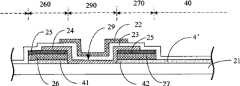
Fig. 3 is the plane graph of TFT-LCD array base palte of the present invention, and what reflected is the structure of a pixel cell.As shown in Figure 3, present embodiment TFT-LCD array base palte mainly comprises grid line 1 ', data wire 2 ', TFT3 ' and pixel electrode 4 ', orthogonal grid line 1 ' and data wire 2 ' have defined pixel cell, TFT3 ' and pixel electrode 4 ' are formed in the pixel cell, grid line 1 ' is used for providing start signal to TFT3 ', and data wire 2 ' is used for providing data-signal topixel electrode 4 '.TFT3 ' is the active switch element.
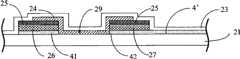
Fig. 4 be among Fig. 3 A1-A1 to profile, what reflected is the structure of TFT.As shown in Figure 4, TFT of the present invention comprises: transparency carrier 21, the first electrically conducting transparent portion 41, the second electrically conducting transparent portion 42, source electrode 26, drain electrode 27, doping semiconductor layer 25, semiconductor layer 24, gate insulation layer 23 and gate electrode 22.Wherein, the first electrically conducting transparent portion 41 is arranged on the source electrode zone 260, and the first electrically conducting transparent portion 41 is not connected with pixel electrode 4 '; The first electrically conducting transparent portion 41 is provided with source electrode 26; The second electrically conducting transparent portion 42 is arranged at drain electrode zone 270, and the second electrically conducting transparent portion 42 forms with pixel electrode 4 ' one; The second electrically conducting transparent portion 42 is provided with drain electrode 27; Be respectively arranged with doping semiconductor layer 25 on source electrode 26 and the drain electrode 27, between source electrode 26 and drain electrode 27, have the TFT channel region; Doping semiconductor layer 25 is provided with semiconductor layer 24, and semiconductor layer 24 also is arranged on the TFT channel region 290, forms TFT raceway groove 29; Gate insulation layer 23 is arranged on the said structure figure and covers whole transparency carrier 21; Gate insulation layer 23 is provided with gate electrode 22, and gate electrode 22 is positioned at the top of TFT channel region, and is connected with grid line 1 '.
Technique scheme of the present invention is a kind of top gate electrode structure, can adopt three composition prepared to finish, advantage such as have that processing step is simplified, the process time is short, production efficiency is high and production cost is low.In addition, compare the method for existing three composition technology manufacturing array substrates, the present invention need not to peel off (lift off) technology, has simplified technology difficulty greatly, has improved yield of products.
Fig. 5-Figure 18 has illustrated the manufacturing process of TFT-LCD array base palte of the present invention successively.
Fig. 5 is the profile after metallic film and doped semiconductor films are leaked in deposit transparent conductive film, source on the transparency carrier.As shown in Figure 5, at first adopt plasma reinforced chemical vapour deposition (PECVD), magnetron sputtering, thermal evaporation or other film build method,metallic film 200 and dopedsemiconductor films 300 are leaked in deposit transparentconductive film 100, source successively on transparency carrier 21 (as glass substrate or quartz base plate).It can be the single thin film that metals such as molybdenum, aluminium, aluminium neodymium alloy, tungsten, chromium, copper form thatmetallic film 200 is leaked in the source, also can be the plural layers that above metallic multilayer deposition forms.Transparentconductive film 100 can be ITO, IZO etc.
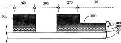
Fig. 6 has been for after having applied photoresist on the structure of Fig. 5, and photoresist has been carried out profile after exposure and the development treatment.As shown in Figure 6, coating onedeck photoresist 1000 on dopedsemiconductor films 300, by two accent (dual tone) mask plate (partly transferring mask plate or tone mask plate)photoresist 1000 is exposed and development treatment, make thephotoresist 1000 in data wire zone (not shown),source electrode zone 260 anddrain electrode zone 270 have the first thickness H, thephotoresist 1000 ofpixel electrode area 40 has second thickness h, the described first thickness H is greater than second thickness h, and there is not photoresist in all the other zones.
Fig. 7 is for having carried out the profile behind first etching technics to the structure of Fig. 6.As shown in Figure 7, leakmetallic film 200 and transparentconductive film 100 by all the other regional dopedsemiconductor films 300, source that first etching technics etches away outsidepixel electrode area 40, data wire zone,source electrode zone 260 and thedrain electrode zone 270 fully, promptly etch away all the other the regional dopedsemiconductor films 300, the source that do not coverphotoresist 1000 and leakmetallic film 200 and transparent conductive film 100.Be specially, pass through SF6, HCl, Cl2, gas such as He carries out etching to doped semiconductor films 300 (n+a-Si:H); The etching agent that mixture by phosphoric acid and nitric acid makes leaksmetallic film 200 to the source and carries out etching; By etching agents such as sulfuric acid or peroxide transparent conductive film 100 (ITO or IZO) is carried out etching.
Wherein, if when adopting the Mo can carry out dry etching or Mo/Al/Mo to leakmetallic film 200 as the source,metallic film 200 is leaked in dopedsemiconductor films 300 and source can carry out continuous dry etching, also can carry out the scheme that dry etching connects wet etching.This lithographic method can change according to the kind that metallic film is leaked in the source.
Fig. 8 is for having carried out cineration technics profile afterwards to the photoresist among Fig. 7.As shown in Figure 8, removed thephotoresist 1000 of the second thickness h degree, exposed thedoped semiconductor films 300 ofpixel electrode area 40 by the cineration technics of photoresist, remainingphotoresist 1000 also correspondingly attenuation the second thickness h degree.
Fig. 9 is for having carried out the profile behind second etching technics to the structure of Fig. 8.As shown in Figure 9,metallic film 200 is leaked in thedoped semiconductor films 300, the source that etch awaypixel electrode area 40 by second etching technics fully, the first electrically conductingtransparent portion 41, the second electrically conductingtransparent portion 42 have been formed, pixel electrode 4 ',source electrode 26,drain electrode 27 anddoping semiconductor layer 25.
Figure 10 is for having peeled off the profile behind the residue photoresist on the structure of Fig. 9.
So far, finished the first composition technology by Fig. 5 to Figure 10.
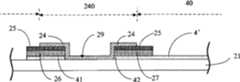
Figure 11 is for having deposited the profile behind the semiconductive thin film on the structure of Figure 10.Usually can adopt PECVD or other film build method, deposition layer of semiconductor film 400.After this deposition, in the data wire zone,source electrode zone 260 anddrain electrode zone 270 semiconductivethin films 400 are deposited on thedoping semiconductor layer 25, be deposited on thepixel electrode 40 atpixel electrode area 40 semiconductivethin films 400, (comprise TFT channel region 290) in other zone, semiconductivethin film 400 is deposited on thetransparency carrier 21.
Figure 12 is the profile after applying photoresist on the structure of Figure 11.Apply photoresist 2000 earlier on semiconductivethin film 400, by common mask plate,photoresist 2000 is exposed and development treatment then, makephotoresist 2000 cover on thesemiconductor regions 240, other zone does not have the residue photoresist.As shown in figure 12,semiconductor regions 240 comprisesTFT channel region 290 and all or part ofsource electrode zone 260 anddrain electrode zone 270.
Figure 13 is for carrying out the profile behind the etching technics to the structure of Figure 12.As shown in figure 13, etch away the semiconductivethin film 400 that does not have photoresist to cover, formed the figure ofsemiconductor layer 24 by etching agent.Among Figure 11,semiconductor layer 24 is formed on thesource electrode zone 260 anddrain electrode zone 270 ofTFT channel region 290 and part.Thesemiconductor layer 24 that is positioned on theTFT channel region 290 has formed TFT raceway groove 29.Then, peeled off the remaining photoresist shown in Figure 12.
So far, finished the second composition technology by Figure 11 to Figure 13.
Figure 14 is the profile behind deposition insulation film on the structure of Figure 13.As shown in figure 14, adopt PECVD or other film build method deposition one deck insulation film, formgate insulation layer 23 at whole transparency carrier 21.Insulation film can adopt the single thin film of SiNx, SiOx or SiOxNy, or the plural layers of above-mentioned material multilayer deposition formation.
Figure 15 is the profile behind deposition grid metallic film on the structure of Figure 14.As shown in figure 15, can adopt magnetron sputtering, thermal evaporation or other film build method, deposition one deck gridmetallic film 500, gridmetallic film 500 can be the single thin film that metals such as molybdenum, aluminium, aluminium neodymium alloy, tungsten, chromium, copper form, and also can be the plural layers that above metallic multilayer deposition forms.
Figure 16 is the profile that applies on the structure of Figure 15 behind the photoresist.As shown in figure 16, on gridmetallic film 500, applyphotoresist 3000 earlier, by common mask plate,photoresist 3000 is exposed and development treatment then, makephotoresist 3000 cover grid region (not shown) and gate electrode zone 220, other zone does not have the residue photoresist.Gate electrode zone 220 comprises wholeTFT channel regions 290 and all or part ofsource electrode zone 260 anddrain electrode zone 270.
Figure 17 is for carrying out the profile behind the etching technics to the structure of Figure 16.As shown in figure 17, etch away the gridmetallic film 500 that does not havephotoresist 3000 to cover, formed the figure ofgate electrode 22 and grid line by etching agent.
Figure 18 is the profile behind the photoresist that peels off among Figure 17.
So far, finished the 3rd composition technology, obtained TFT-LCD array base palte of the present invention by Figure 14 to Figure 18.
The present invention is because behind first deposit transparent conductive film, source leakage metallic film and the doped semiconductor films, carry out the cineration technics of photoresist, the deposit transparent conductive layer is compared after carrying out photoresist ashing technology compared to existing technology, avoided the pollution of cineration technics, improved yield of products transparency conducting layer.
It should be noted that at last: above embodiment is only in order to technical scheme of the present invention to be described but not limit it, although the present invention is had been described in detail with reference to preferred embodiment, those of ordinary skill in the art is to be understood that: it still can make amendment or be equal to replacement technical scheme of the present invention, and these modifications or be equal to replacement and also can not make amended technical scheme break away from the spirit and scope of technical solution of the present invention.
Claims (10)
Translated fromChinesePriority Applications (4)
| Application Number | Priority Date | Filing Date | Title |
|---|---|---|---|
| CN2009100855066ACN101894807B (en) | 2009-05-22 | 2009-05-22 | TFT-LCD (Thin Film Transistor-Liquid Crystal Display) array base plate and manufacturing method thereof |
| US12/784,759US8298878B2 (en) | 2009-05-22 | 2010-05-21 | TFT-LCD array substrate and manufacturing method thereof |
| KR1020100048076AKR101154488B1 (en) | 2009-05-22 | 2010-05-24 | Tft-lcd array substrate and manufacturing method thereof |
| JP2010118333AJP5588740B2 (en) | 2009-05-22 | 2010-05-24 | TFT-LCD array substrate and manufacturing method thereof |
Applications Claiming Priority (1)
| Application Number | Priority Date | Filing Date | Title |
|---|---|---|---|
| CN2009100855066ACN101894807B (en) | 2009-05-22 | 2009-05-22 | TFT-LCD (Thin Film Transistor-Liquid Crystal Display) array base plate and manufacturing method thereof |
Publications (2)
| Publication Number | Publication Date |
|---|---|
| CN101894807Atrue CN101894807A (en) | 2010-11-24 |
| CN101894807B CN101894807B (en) | 2012-11-21 |
Family
ID=43103953
Family Applications (1)
| Application Number | Title | Priority Date | Filing Date |
|---|---|---|---|
| CN2009100855066AExpired - Fee RelatedCN101894807B (en) | 2009-05-22 | 2009-05-22 | TFT-LCD (Thin Film Transistor-Liquid Crystal Display) array base plate and manufacturing method thereof |
Country Status (4)
| Country | Link |
|---|---|
| US (1) | US8298878B2 (en) |
| JP (1) | JP5588740B2 (en) |
| KR (1) | KR101154488B1 (en) |
| CN (1) | CN101894807B (en) |
Cited By (21)
| Publication number | Priority date | Publication date | Assignee | Title |
|---|---|---|---|---|
| CN102487041A (en)* | 2010-12-02 | 2012-06-06 | 京东方科技集团股份有限公司 | Array substrate, manufacturing method thereof, and electronic paper display |
| CN102540534A (en)* | 2010-12-13 | 2012-07-04 | 京东方科技集团股份有限公司 | Electronic paper display substrate, manufacturing method thereof and electronic paper display |
| CN102629611A (en)* | 2012-03-29 | 2012-08-08 | 京东方科技集团股份有限公司 | Display device, array substrate and manufacturing method thereof |
| CN102651403A (en)* | 2012-04-16 | 2012-08-29 | 京东方科技集团股份有限公司 | Thin film transistor, array substrate and manufacturing method of array substrate and display panel |
| CN102655155A (en)* | 2012-02-27 | 2012-09-05 | 京东方科技集团股份有限公司 | Array substrate, manufacturing method and display device thereof |
| CN102692752A (en)* | 2012-06-07 | 2012-09-26 | 深圳市华星光电技术有限公司 | Liquid crystal display panel and manufacturing method thereof |
| CN102709237A (en)* | 2012-03-05 | 2012-10-03 | 京东方科技集团股份有限公司 | Thin-film transistor array substrate and manufacturing method and electronic devices thereof |
| CN102709234A (en)* | 2011-08-19 | 2012-10-03 | 京东方科技集团股份有限公司 | Thin film transistor (TFT) array substrate and manufacturing method thereof, and electronic device |
| CN102779784A (en)* | 2012-06-15 | 2012-11-14 | 上海大学 | Thin film transistor array substrate manufacturing method |
| CN103022148A (en)* | 2012-12-14 | 2013-04-03 | 京东方科技集团股份有限公司 | Array substrate, manufacture method of array substrate and display device |
| WO2013091306A1 (en)* | 2011-12-21 | 2013-06-27 | 深圳市华星光电技术有限公司 | Thin film transistor substrate and manufacturing method thereof and liquid crystal display device |
| WO2014005348A1 (en)* | 2012-07-02 | 2014-01-09 | 深圳市华星光电技术有限公司 | Manufacturing method for array substrate, array substrate and liquid crystal display device |
| US8900938B2 (en) | 2012-07-02 | 2014-12-02 | Shenzhen China Star Optoelectronics Technology Co., Ltd. | Manufacturing method of array substrate, array substrate and LCD device |
| CN105161505A (en)* | 2015-09-28 | 2015-12-16 | 京东方科技集团股份有限公司 | Array substrate, manufacturing method thereof and display panel |
| CN106384714A (en)* | 2016-10-13 | 2017-02-08 | 京东方科技集团股份有限公司 | Thin film transistor, manufacturing method thereof, and array substrate |
| WO2017028461A1 (en)* | 2015-08-14 | 2017-02-23 | 京东方科技集团股份有限公司 | Preparation method for thin film transistor, preparation method for array substrate, array substrate, and display apparatus |
| CN106935660A (en)* | 2017-05-12 | 2017-07-07 | 京东方科技集团股份有限公司 | Thin film transistor (TFT) and preparation method thereof, array base palte and display device |
| KR20170096007A (en)* | 2014-12-30 | 2017-08-23 | 센젠 차이나 스타 옵토일렉트로닉스 테크놀로지 컴퍼니 리미티드 | Array substrate, display panel, and manufacturing method for array substrate |
| CN107731928A (en)* | 2016-08-11 | 2018-02-23 | 创王光电股份有限公司 | Vertical structure thin film transistor and method of manufacturing the same |
| CN108878626A (en)* | 2018-06-29 | 2018-11-23 | 京东方科技集团股份有限公司 | A kind of display panel and production method, display device |
| CN109192704A (en)* | 2018-09-05 | 2019-01-11 | 京东方科技集团股份有限公司 | Array substrate and its manufacturing method, display device |
Families Citing this family (11)
| Publication number | Priority date | Publication date | Assignee | Title |
|---|---|---|---|---|
| CN102608859B (en) | 2011-01-21 | 2017-02-01 | 京东方科技集团股份有限公司 | Mask plate and method for applying it to manufacture thin film transistor array substrate |
| CN102768989A (en)* | 2011-05-06 | 2012-11-07 | 京东方科技集团股份有限公司 | Thin film transistor array substrate structure and manufacturing method |
| CN102629585B (en)* | 2011-11-17 | 2014-07-23 | 京东方科技集团股份有限公司 | Display device, thin film transistor, array substrate and manufacturing method thereof |
| US20130162925A1 (en)* | 2011-12-21 | 2013-06-27 | Shenzhen China Star Optoelectronics Technology Co. Ltd | Thin-film Transistor Substrate and Manufacturing Method Thereof and Liquid Crystal Display Device |
| CN102779785A (en)* | 2012-07-25 | 2012-11-14 | 京东方科技集团股份有限公司 | Organic thin film transistor array substrate and manufacturing method thereof, and display device |
| CN103050497A (en)* | 2012-12-27 | 2013-04-17 | 青岛龙泰天翔通信科技有限公司 | Flexible driving back plate |
| CN103456742B (en)* | 2013-08-27 | 2017-02-15 | 京东方科技集团股份有限公司 | Array substrate, manufacturing method of array substrate and display device |
| CN103489877B (en)* | 2013-09-30 | 2015-12-09 | 北京京东方光电科技有限公司 | Array base palte and manufacture method thereof and display unit |
| CN105097548A (en)* | 2015-06-23 | 2015-11-25 | 京东方科技集团股份有限公司 | Oxide thin film transistor, array substrate, and respective preparation method and display device |
| GB2566673B (en)* | 2017-07-21 | 2022-10-26 | Flexenable Ltd | Thin-Film Transistor (TFT) Architecture for Liquid Crystal Displays |
| CN107731882A (en)* | 2017-11-07 | 2018-02-23 | 深圳市华星光电半导体显示技术有限公司 | A kind of organic thin film transistor array substrate and preparation method thereof, display device |
Family Cites Families (14)
| Publication number | Priority date | Publication date | Assignee | Title |
|---|---|---|---|---|
| JPS61183622A (en)* | 1985-02-08 | 1986-08-16 | Seiko Instr & Electronics Ltd | Thin film transistor device and its manufacture |
| JPH079994B2 (en)* | 1986-10-30 | 1995-02-01 | カシオ計算機株式会社 | Method for manufacturing active matrix liquid crystal display device |
| JPH06252171A (en) | 1993-03-02 | 1994-09-09 | Hitachi Ltd | Manufacturing method of active matrix panel |
| JPH07162007A (en)* | 1993-12-10 | 1995-06-23 | Sharp Corp | Manufacturing method of active matrix substrate |
| KR0136066B1 (en)* | 1994-05-06 | 1998-04-24 | 한민구 | Manufacturing method of thin film transistor having offset structure |
| JP2965283B2 (en)* | 1994-07-13 | 1999-10-18 | ヒュンダイ エレクトロニクス インダストリーズ カムパニー リミテッド | Method for manufacturing thin film transistor |
| KR100259078B1 (en)* | 1997-08-14 | 2000-06-15 | 김영환 | Thin film transistor and its manufacturing method |
| KR100467176B1 (en)* | 2000-10-11 | 2005-01-24 | 엘지.필립스 엘시디 주식회사 | Array pannel of liquid crystal display and fabricating method the same |
| KR100773239B1 (en)* | 2000-12-29 | 2007-11-02 | 엘지.필립스 엘시디 주식회사 | LCD and its manufacturing method |
| KR100710282B1 (en)* | 2000-12-29 | 2007-04-23 | 엘지.필립스 엘시디 주식회사 | Thin film transistor and its manufacturing method |
| US6849492B2 (en)* | 2002-07-08 | 2005-02-01 | Micron Technology, Inc. | Method for forming standard voltage threshold and low voltage threshold MOSFET devices |
| US7344928B2 (en)* | 2005-07-28 | 2008-03-18 | Palo Alto Research Center Incorporated | Patterned-print thin-film transistors with top gate geometry |
| TWI316759B (en)* | 2006-01-09 | 2009-11-01 | Univ Nat Chiao Tung | Mothod for fabricatng a straggered source/drain and thin-channel tft |
| JP5244364B2 (en)* | 2007-10-16 | 2013-07-24 | 株式会社半導体エネルギー研究所 | Semiconductor device and manufacturing method thereof |
- 2009
- 2009-05-22CNCN2009100855066Apatent/CN101894807B/ennot_activeExpired - Fee Related
- 2010
- 2010-05-21USUS12/784,759patent/US8298878B2/ennot_activeExpired - Fee Related
- 2010-05-24KRKR1020100048076Apatent/KR101154488B1/ennot_activeExpired - Fee Related
- 2010-05-24JPJP2010118333Apatent/JP5588740B2/ennot_activeExpired - Fee Related
Cited By (45)
| Publication number | Priority date | Publication date | Assignee | Title |
|---|---|---|---|---|
| CN102487041A (en)* | 2010-12-02 | 2012-06-06 | 京东方科技集团股份有限公司 | Array substrate, manufacturing method thereof, and electronic paper display |
| CN102540534A (en)* | 2010-12-13 | 2012-07-04 | 京东方科技集团股份有限公司 | Electronic paper display substrate, manufacturing method thereof and electronic paper display |
| US8861070B2 (en) | 2010-12-13 | 2014-10-14 | Boe Technology Group Co., Ltd. | Electronic paper display substrate and the manufacturing method thereof |
| CN102540534B (en)* | 2010-12-13 | 2015-05-13 | 京东方科技集团股份有限公司 | Electronic paper display substrate, manufacturing method thereof and electronic paper display |
| CN102709234B (en)* | 2011-08-19 | 2016-02-17 | 京东方科技集团股份有限公司 | Thin-film transistor array base-plate and manufacture method thereof and electronic device |
| US8895334B2 (en) | 2011-08-19 | 2014-11-25 | Boe Technology Group Co., Ltd. | Thin film transistor array substrate and method for manufacturing the same and electronic device |
| CN102709234A (en)* | 2011-08-19 | 2012-10-03 | 京东方科技集团股份有限公司 | Thin film transistor (TFT) array substrate and manufacturing method thereof, and electronic device |
| WO2013091306A1 (en)* | 2011-12-21 | 2013-06-27 | 深圳市华星光电技术有限公司 | Thin film transistor substrate and manufacturing method thereof and liquid crystal display device |
| US9905787B2 (en) | 2012-02-27 | 2018-02-27 | Boe Technology Group Co., Ltd. | Array substrate, method for manufacturing the same and display device |
| CN102655155B (en)* | 2012-02-27 | 2015-03-11 | 京东方科技集团股份有限公司 | Array substrate, manufacturing method and display device thereof |
| CN102655155A (en)* | 2012-02-27 | 2012-09-05 | 京东方科技集团股份有限公司 | Array substrate, manufacturing method and display device thereof |
| CN102709237A (en)* | 2012-03-05 | 2012-10-03 | 京东方科技集团股份有限公司 | Thin-film transistor array substrate and manufacturing method and electronic devices thereof |
| WO2013131384A1 (en)* | 2012-03-05 | 2013-09-12 | 京东方科技集团股份有限公司 | Thin-film transistor array substrate, manufacturing method therefor, and electronic device |
| CN102709237B (en)* | 2012-03-05 | 2014-06-25 | 京东方科技集团股份有限公司 | Thin-film transistor array substrate and manufacturing method and electronic devices thereof |
| US8952387B2 (en) | 2012-03-05 | 2015-02-10 | Boe Technology Group Co., Ltd. | Thin film transistor array substrate and method for manufacturing the same |
| US9230995B2 (en) | 2012-03-29 | 2016-01-05 | Boe Technology Group Co., Ltd. | Array substrate, manufacturing method thereof and display device |
| CN102629611A (en)* | 2012-03-29 | 2012-08-08 | 京东方科技集团股份有限公司 | Display device, array substrate and manufacturing method thereof |
| CN102629611B (en)* | 2012-03-29 | 2015-01-21 | 京东方科技集团股份有限公司 | Display device, array substrate and manufacturing method thereof |
| WO2013155835A1 (en)* | 2012-04-16 | 2013-10-24 | 京东方科技集团股份有限公司 | Thin film transistor, array substrate and manufacturing method of array substrate, and display panel |
| US9166059B2 (en) | 2012-04-16 | 2015-10-20 | Boe Technology Group Co., Ltd. | Thin film transistor, array substrate and manufacturing method thereof, and display panel |
| CN102651403A (en)* | 2012-04-16 | 2012-08-29 | 京东方科技集团股份有限公司 | Thin film transistor, array substrate and manufacturing method of array substrate and display panel |
| CN102692752B (en)* | 2012-06-07 | 2015-03-25 | 深圳市华星光电技术有限公司 | Liquid crystal display panel and manufacturing method thereof |
| WO2013181864A1 (en)* | 2012-06-07 | 2013-12-12 | 深圳市华星光电技术有限公司 | Liquid crystal display panel and producing method thereof |
| CN102692752A (en)* | 2012-06-07 | 2012-09-26 | 深圳市华星光电技术有限公司 | Liquid crystal display panel and manufacturing method thereof |
| CN102779784A (en)* | 2012-06-15 | 2012-11-14 | 上海大学 | Thin film transistor array substrate manufacturing method |
| US8900938B2 (en) | 2012-07-02 | 2014-12-02 | Shenzhen China Star Optoelectronics Technology Co., Ltd. | Manufacturing method of array substrate, array substrate and LCD device |
| WO2014005348A1 (en)* | 2012-07-02 | 2014-01-09 | 深圳市华星光电技术有限公司 | Manufacturing method for array substrate, array substrate and liquid crystal display device |
| CN103022148A (en)* | 2012-12-14 | 2013-04-03 | 京东方科技集团股份有限公司 | Array substrate, manufacture method of array substrate and display device |
| CN103022148B (en)* | 2012-12-14 | 2016-01-13 | 京东方科技集团股份有限公司 | A kind of array base palte and preparation method thereof, display unit |
| KR20170096007A (en)* | 2014-12-30 | 2017-08-23 | 센젠 차이나 스타 옵토일렉트로닉스 테크놀로지 컴퍼니 리미티드 | Array substrate, display panel, and manufacturing method for array substrate |
| KR101999907B1 (en) | 2014-12-30 | 2019-07-12 | 센젠 차이나 스타 옵토일렉트로닉스 테크놀로지 컴퍼니 리미티드 | Array substrate, display panel, and manufacturing method for array substrate |
| US10120256B2 (en) | 2015-08-14 | 2018-11-06 | Boe Technology Group Co., Ltd. | Preparation method for thin film transistor, preparation method for array substrate, array substrate, and display apparatus |
| WO2017028461A1 (en)* | 2015-08-14 | 2017-02-23 | 京东方科技集团股份有限公司 | Preparation method for thin film transistor, preparation method for array substrate, array substrate, and display apparatus |
| US10304861B2 (en) | 2015-09-28 | 2019-05-28 | Boe Technology Group Co., Ltd. | Array substrate and method of manufacturing the same, and display panel |
| CN105161505A (en)* | 2015-09-28 | 2015-12-16 | 京东方科技集团股份有限公司 | Array substrate, manufacturing method thereof and display panel |
| CN107731928A (en)* | 2016-08-11 | 2018-02-23 | 创王光电股份有限公司 | Vertical structure thin film transistor and method of manufacturing the same |
| CN107731928B (en)* | 2016-08-11 | 2020-08-14 | 创王光电股份有限公司 | Vertical structure thin film transistor and its manufacturing method |
| CN106384714B (en)* | 2016-10-13 | 2018-07-10 | 京东方科技集团股份有限公司 | Thin film transistor (TFT) and preparation method thereof, array substrate |
| CN106384714A (en)* | 2016-10-13 | 2017-02-08 | 京东方科技集团股份有限公司 | Thin film transistor, manufacturing method thereof, and array substrate |
| WO2018205886A1 (en)* | 2017-05-12 | 2018-11-15 | 京东方科技集团股份有限公司 | Thin film transistor and manufacturing method therefor, array substrate and display apparatus |
| CN106935660A (en)* | 2017-05-12 | 2017-07-07 | 京东方科技集团股份有限公司 | Thin film transistor (TFT) and preparation method thereof, array base palte and display device |
| CN106935660B (en)* | 2017-05-12 | 2019-10-18 | 京东方科技集团股份有限公司 | Thin film transistor and manufacturing method thereof, array substrate and display device |
| US10833107B2 (en) | 2017-05-12 | 2020-11-10 | Boe Technology Group Co., Ltd. | Thin film transistor, manufacturing method therefor, array substrate and display device |
| CN108878626A (en)* | 2018-06-29 | 2018-11-23 | 京东方科技集团股份有限公司 | A kind of display panel and production method, display device |
| CN109192704A (en)* | 2018-09-05 | 2019-01-11 | 京东方科技集团股份有限公司 | Array substrate and its manufacturing method, display device |
Also Published As
| Publication number | Publication date |
|---|---|
| KR20100126228A (en) | 2010-12-01 |
| CN101894807B (en) | 2012-11-21 |
| KR101154488B1 (en) | 2012-06-13 |
| JP2010271718A (en) | 2010-12-02 |
| JP5588740B2 (en) | 2014-09-10 |
| US8298878B2 (en) | 2012-10-30 |
| US20100295049A1 (en) | 2010-11-25 |
Similar Documents
| Publication | Publication Date | Title |
|---|---|---|
| CN101894807A (en) | TFT-LCD (Thin Film Transistor-Liquid Crystal Display) array base plate and manufacturing method thereof | |
| CN100517075C (en) | A method for manufacturing an array substrate of a thin film transistor liquid crystal display | |
| CN101685229B (en) | Method for manufacturing liquid crystal display array substrate | |
| US8298883B2 (en) | Method of forming photoresist burr edge and method of manufacturing array substrate | |
| CN101630098B (en) | TFT-LCD array substrate and manufacturing method thereof | |
| CN103489877B (en) | Array base palte and manufacture method thereof and display unit | |
| CN102738007B (en) | Manufacturing method of thin film transistor and manufacturing method of array base plate | |
| US20120181557A1 (en) | Array substrate and method for manufacturing the same | |
| CN103762199B (en) | A kind of manufacture method of array base palte of liquid crystal display | |
| CN103928406B (en) | The preparation method of array base palte, array base palte, display device | |
| JP2007318144A (en) | TFT-LCD array substrate structure and manufacturing method thereof | |
| CN101957529A (en) | FFS (Fringe Field Switching) type TFT-LCD (Thin Film Transistor Liquid Crystal Display) array substrate and manufacturing method thereof | |
| CN102148196A (en) | TFT-LCD (thin film transistor-liquid crystal display) array substrate and manufacturing method therefor | |
| CN102629584B (en) | Array substrate and manufacturing method thereof and display device | |
| CN103715096A (en) | Thin film thyristor and manufacturing method thereof and array substrate and manufacturing method thereof | |
| CN102034751B (en) | TFT-LCD array substrate and manufacturing method thereof | |
| US20100208156A1 (en) | Tft-lcd array substrate and method of manufacturing the same | |
| CN106783885A (en) | The preparation method of TFT substrate | |
| CN102768990B (en) | Array substrate, and manufacturing method and display device of array substrate | |
| CN103107133A (en) | Array substrate, manufacturing method thereof and displaying device | |
| CN101963726B (en) | FFS (Fringe Field Switching) type TFT-LCD (Thin Film Transistor-Liquid Crystal Display) array base plate and manufacturing method thereof | |
| CN102629588B (en) | Method for manufacturing array substrate | |
| CN102543892B (en) | Thin film transistor substrate and manufacturing method thereof and liquid crystal display device | |
| TWI396916B (en) | Thin film transistor array substrate manufacturing method | |
| CN102637631B (en) | Manufacturing method of TFT (thin film transistor)-LCD (liquid crystal display) array substrate |
Legal Events
| Date | Code | Title | Description |
|---|---|---|---|
| C06 | Publication | ||
| PB01 | Publication | ||
| C10 | Entry into substantive examination | ||
| SE01 | Entry into force of request for substantive examination | ||
| C14 | Grant of patent or utility model | ||
| GR01 | Patent grant | ||
| ASS | Succession or assignment of patent right | Owner name:BEIJING BOE PHOTOELECTRICITY SCIENCE + TECHNOLOGY Effective date:20150626 Owner name:JINGDONGFANG SCIENCE AND TECHNOLOGY GROUP CO., LTD Free format text:FORMER OWNER: BEIJING BOE PHOTOELECTRICITY SCIENCE + TECHNOLOGY CO., LTD. Effective date:20150626 | |
| C41 | Transfer of patent application or patent right or utility model | ||
| TR01 | Transfer of patent right | Effective date of registration:20150626 Address after:100015 Jiuxianqiao Road, Beijing, No. 10, No. Patentee after:BOE TECHNOLOGY GROUP Co.,Ltd. Patentee after:BEIJING BOE OPTOELECTRONICS TECHNOLOGY Co.,Ltd. Address before:100176 Beijing economic and Technological Development Zone, West Central Road, No. 8 Patentee before:BEIJING BOE OPTOELECTRONICS TECHNOLOGY Co.,Ltd. | |
| CF01 | Termination of patent right due to non-payment of annual fee | ||
| CF01 | Termination of patent right due to non-payment of annual fee | Granted publication date:20121121 |