CN101888247A - Adaptive Calibration Device for Mismatch Error of Time Alternating Analog-to-Digital Converter - Google Patents
Adaptive Calibration Device for Mismatch Error of Time Alternating Analog-to-Digital ConverterDownload PDFInfo
- Publication number
- CN101888247A CN101888247ACN2010102250569ACN201010225056ACN101888247ACN 101888247 ACN101888247 ACN 101888247ACN 2010102250569 ACN2010102250569 ACN 2010102250569ACN 201010225056 ACN201010225056 ACN 201010225056ACN 101888247 ACN101888247 ACN 101888247A
- Authority
- CN
- China
- Prior art keywords
- reference signal
- signal
- self
- analog
- channel
- Prior art date
- Legal status (The legal status is an assumption and is not a legal conclusion. Google has not performed a legal analysis and makes no representation as to the accuracy of the status listed.)
- Granted
Links
- 230000003044adaptive effectEffects0.000titleclaimsabstractdescription38
- 230000008521reorganizationEffects0.000claimsabstractdescription7
- 238000005457optimizationMethods0.000claimsabstractdescription5
- 238000005070samplingMethods0.000claimsdescription22
- 230000001360synchronised effectEffects0.000claimsdescription10
- 238000006243chemical reactionMethods0.000claimsdescription6
- 238000001914filtrationMethods0.000claimsdescription5
- 238000012549trainingMethods0.000claimsdescription4
- 230000015572biosynthetic processEffects0.000claims1
- 230000008520organizationEffects0.000claims1
- 238000005215recombinationMethods0.000abstractdescription10
- 230000006798recombinationEffects0.000abstractdescription10
- 230000000694effectsEffects0.000abstractdescription4
- 238000012545processingMethods0.000abstractdescription4
- 238000004364calculation methodMethods0.000description9
- 238000010586diagramMethods0.000description8
- 238000000034methodMethods0.000description8
- 238000013461designMethods0.000description7
- 230000004044responseEffects0.000description5
- 230000008569processEffects0.000description4
- 238000001228spectrumMethods0.000description3
- 238000005259measurementMethods0.000description2
- 238000013459approachMethods0.000description1
- 238000004891communicationMethods0.000description1
- 238000012937correctionMethods0.000description1
- 125000004122cyclic groupChemical group0.000description1
- 238000011161developmentMethods0.000description1
- 238000005516engineering processMethods0.000description1
- 230000007274generation of a signal involved in cell-cell signalingEffects0.000description1
- 230000006872improvementEffects0.000description1
- 238000004519manufacturing processMethods0.000description1
- 238000007493shaping processMethods0.000description1
- 230000003595spectral effectEffects0.000description1
- 230000003068static effectEffects0.000description1
- 238000003860storageMethods0.000description1
- 238000012360testing methodMethods0.000description1
Images


Landscapes
- Analogue/Digital Conversion (AREA)
Abstract
Translated fromChinese
Description
Translated fromChinese技术领域technical field
本发明涉及一种校准装置,具体涉及应用于多通道时间交替模数转换器(TIADC)的一种自适应校准装置,能够校准TIADC中多个通道之间的失配误差。The invention relates to a calibration device, in particular to an adaptive calibration device applied to a multi-channel time-alternating analog-to-digital converter (TIADC), capable of calibrating mismatch errors between multiple channels in the TIADC.
背景技术Background technique
采用多个相对低速、高精度的模数转换器(ADC)多个通道并行时间交替采样构成TIADC系统是目前高速、高精ADC的发展方向。但在实际应用中,ADC的制造工艺等引入通道失配误差(时间误差、增益误差和偏置误差),失配误差如果不加以校准,就会严重影响TIADC系统的性能。申请专利号为200510094743.0自校准多通道模数转换器给出了校准增益误差和偏置误差的方法;申请专利号为200510122833.6四通道无失配时钟控制电路提供了一种减小时间误差的时钟控制电路,这种方法要求采样保持电路必须以系统的采样速度运行,而设计高速高精度的采样保持电路是很困难的,限制了TIADC系统的采样速度。美国专利US2008174461-A1在模拟域从设计ADC的角度减小TIADC的失配误差,对于现有ADC芯片则不具有通用性。美国专利US2008030387-A1只能校准增益误差;US2008024338-A1只能校准增益误差和偏置误差。Using multiple relatively low-speed, high-precision analog-to-digital converters (ADCs) and multiple channels for parallel time-alternating sampling to form a TIADC system is the current development direction of high-speed, high-precision ADCs. However, in practical applications, the manufacturing process of the ADC introduces channel mismatch errors (time error, gain error, and offset error). If the mismatch error is not calibrated, it will seriously affect the performance of the TIADC system. The patent application number is 200510094743.0. The self-calibrating multi-channel analog-to-digital converter provides a method for calibrating gain errors and offset errors; the patent application number is 200510122833.6. The four-channel mismatch-free clock control circuit provides a clock control that reduces time errors circuit, this method requires that the sample-and-hold circuit must run at the sampling speed of the system, and it is very difficult to design a high-speed and high-precision sample-and-hold circuit, which limits the sampling speed of the TIADC system. US2008174461-A1 reduces the mismatch error of TIADC from the perspective of ADC design in the analog domain, but it is not universal for existing ADC chips. US2008030387-A1 can only calibrate gain error; US2008024338-A1 can only calibrate gain error and offset error.
M个采样速率为fs的ADC并行交替工作,构成采样速率为Fs(Fs=Mfs)的TIADC系统,此时TIADC系统可以处理的模拟输入信号的带宽为Fs/2。但对于每个通道的ADC可以处理的最大带宽为fs/2,也就是说当输入信号带宽小于fs/2才可以保证每个ADC的输出不混叠。由于增益误差和偏置误差是线性的,因此可以通过在fs/2输入带宽内对单个通道进行补偿然后外推到整个Fs/2输入带宽内。但对于时间误差,在输入带宽小于fs/2时,可以通过注入测试信号计算出时间误差后,利用延时滤波器进行相位补偿。当输入信号的带宽大于fs/2时,每个通道ADC的输出都是混叠的,反映在输出频谱上是大于fs/2的输入信号被折回到fs/2内,此时输出频谱信息已不能真实的反映时间误差信息,因此不能再通过在每个通道上引入延时滤波器进行误差补偿。如何在宽带输入时(输入信号带宽为Fs/2),完成时间误差的校准是本发明目的。M ADCs with a sampling rate of fs work alternately in parallel to form a TIADC system with a sampling rate of Fs (Fs=Mfs). At this time, the bandwidth of the analog input signal that the TIADC system can process is Fs/2. However, the maximum bandwidth that the ADC of each channel can handle is fs/2, that is to say, only when the input signal bandwidth is less than fs/2 can the output of each ADC be guaranteed not to alias. Since the gain error and offset error are linear, they can be compensated by a single channel within the fs/2 input bandwidth and then extrapolated to the full Fs/2 input bandwidth. But for the time error, when the input bandwidth is less than fs/2, the time error can be calculated by injecting the test signal, and then the delay filter can be used for phase compensation. When the bandwidth of the input signal is greater than fs/2, the output of the ADC of each channel is aliased. It is reflected in the output spectrum that the input signal greater than fs/2 is folded back into fs/2. At this time, the output spectrum information has been Time error information cannot be truly reflected, so error compensation can no longer be performed by introducing a delay filter on each channel. How to complete the calibration of the time error at the time of broadband input (input signal bandwidth is Fs/2) is the object of the present invention.
发明内容Contents of the invention
本发明目的是通过提供一种多通道时间交替模数转换器的自适应校准装置,不仅可以校准TIADC系统的增益误差和偏置误差,还可以校准与输入信号频率有关时间误差以及各通道ADC的频率响应失配误差。The purpose of the present invention is to provide an adaptive calibration device for a multi-channel time-alternating analog-to-digital converter, which can not only calibrate the gain error and offset error of the TIADC system, but also calibrate the time error related to the frequency of the input signal and the ADC of each channel. Frequency response mismatch error.
本发明是采用以下技术方案实现的:The present invention is realized by adopting the following technical solutions:
一种时间交替模数转换器(TIADC)失配误差的自适应校准装置,包括时钟产生电路、M通道TIADC、信号重组、自适应重构滤波器组、数字参考信号发生器、模拟参考信号发生器、求差器。本结构有两种工作模式,校准模式和正常工作模式。在校准模式时,M通道TIADC的输入来自参考信号发生器生成的参考信号,M通道TIADC的输出进行信号重组和自适应重构滤波后,送入求差器与内置参考信号发生器产生的参考信号进行求差,所得的误差反馈至自适应重构滤波器组后基于LMS算法调整滤波器的系数,直至误差的数量级满足设计指标要求,校准完成。校准完成后,自适应重构滤波器组的输出与求差器的输入断开,自适应重构滤波器组的系数保持不变,此时输入M通道TIADC的输入接至输入信号进入正常工作模式。A time-alternating analog-to-digital converter (TIADC) adaptive calibration device for mismatch error, including clock generation circuit, M-channel TIADC, signal reconstruction, adaptive reconstruction filter bank, digital reference signal generator, analog reference signal generation device, difference seeker. This structure has two working modes, calibration mode and normal working mode. In the calibration mode, the input of the M-channel TIADC comes from the reference signal generated by the reference signal generator, and the output of the M-channel TIADC is subjected to signal reconstruction and adaptive reconstruction filtering, and then sent to the difference seeker and the reference signal generated by the built-in reference signal generator. The signal is subtracted, and the obtained error is fed back to the adaptive reconstruction filter bank, and then the coefficient of the filter is adjusted based on the LMS algorithm until the order of magnitude of the error meets the requirements of the design index, and the calibration is completed. After the calibration is completed, the output of the adaptive reconstruction filter bank is disconnected from the input of the difference seeker, and the coefficients of the adaptive reconstruction filter bank remain unchanged. At this time, the input of the input M channel TIADC is connected to the input signal to enter normal operation model.
与现有技术相比,本发明具有以下优点:Compared with the prior art, the present invention has the following advantages:
内置同步训练信号并以此为参考信号进行自适应校准,这种自适应校准装置,不需要预先测量或计算通道失配误差的大小,从而避免了失配误差的测量、计算的复杂工作;且不需要区分误差的来源,对各种失配误差均可校准。用各通道重组后的信号对每一个通道进行校准,而不是在各个通道上单独校准,解决了输入信号带宽大于各通道ADC的奈奎斯特频率时由于混叠而不能校准时间误差的问题。采用该结构校准后的TIADC不需要对输入信号进行过采样,即输入信号带宽在系统奈奎斯特采样频率内不受任何因校准算法引入的限制,实现真正意义上的高速率宽带模数转换。校准装置简单,从而避免了复杂的校准算法难于转换为硬件电路的问题,易于硬件实现。校准部分全数字实现,不存在模拟器件的实现偏差问题。校准精度由模拟工艺实现的不可控性转化为校准算法优化的可控性,不会对ADC芯片的设计引入任何限制,通用性强,适用于绝大多数新一代的ADC。The built-in synchronous training signal is used as a reference signal for adaptive calibration. This adaptive calibration device does not need to measure or calculate the size of the channel mismatch error in advance, thus avoiding the complicated work of measuring and calculating the mismatch error; and There is no need to distinguish the source of the error, and it can be calibrated for various mismatch errors. Each channel is calibrated with the recombined signal of each channel, instead of being calibrated separately on each channel, which solves the problem that the time error cannot be calibrated due to aliasing when the bandwidth of the input signal is greater than the Nyquist frequency of the ADC of each channel. The TIADC calibrated with this structure does not need to oversample the input signal, that is, the input signal bandwidth is not subject to any restrictions introduced by the calibration algorithm within the system Nyquist sampling frequency, and realizes a true high-speed broadband analog-to-digital conversion . The calibration device is simple, thereby avoiding the problem that complex calibration algorithms are difficult to convert into hardware circuits, and is easy to realize by hardware. The calibration part is fully digitally implemented, and there is no implementation deviation problem of analog devices. The calibration accuracy is converted from the uncontrollability realized by the analog process to the controllability optimized by the calibration algorithm, which will not introduce any restrictions on the design of the ADC chip, and is highly versatile and applicable to most new generation ADCs.
附图说明Description of drawings
图1为本发明的实施结构框图;Fig. 1 is the implementation structural block diagram of the present invention;
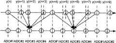
图2为信号重组等效实现示意图,第三个通道ADC#3的无偏值计算;Figure 2 is a schematic diagram of the equivalent realization of signal recombination, and the unbiased value calculation of the third
图3为信号重组等效实现示意图,第四个通道ADC#4的无偏值计算;Figure 3 is a schematic diagram of the equivalent realization of signal recombination, and the unbiased value calculation of the fourth
图4为信号重组等效实现示意图,第二个通道ADC#2的无偏值计算;Figure 4 is a schematic diagram of the equivalent realization of signal recombination, and the unbiased value calculation of the second
图5为本发明的自适应校准装置框图;Fig. 5 is a block diagram of an adaptive calibration device of the present invention;
图6为第一个通道自适应重构滤波器#1的实现结构示意图。Fig. 6 is a schematic diagram of the realization structure of the first channel adaptive
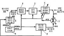
图中,1.M通道TIADC,2.信号重组,3.数字参考信号存储器,4.模拟参考信号发生器,5.自适应重构滤波器组,6.时钟产生电路,7.求差器,8.多路选择器,51.寄存器组,52.子滤波器组。In the figure, 1. M channel TIADC, 2. Signal recombination, 3. Digital reference signal memory, 4. Analog reference signal generator, 5. Adaptive reconstruction filter bank, 6. Clock generation circuit, 7. Difference seeker , 8. Multiplexer, 51. Register bank, 52. Sub-filter bank.
具体实施方式Detailed ways
以下结合附图详细说明本发明的具体实施方式。Specific embodiments of the present invention will be described in detail below in conjunction with the accompanying drawings.
如图1所示,通道个数M=4,每一个通道ADC(ADC#1、ADC#2、ADC#3、ADC#4)的采样速率fs=100MHz,每个ADC的奈奎斯特带宽为50MHz,即当每个ADC的模拟输入带宽小于50MHz时,才能保证每个通道ADC的输出不混叠。4个通道的ADC并行交替工作构成采样速率Fs=400MHz的TIADC系统,转换速率提高4倍,同时系统的奈奎斯特带宽也应提高4倍到200MHz;但当系统的模拟输入带宽大于50MHz时,每个通道的ADC都因不满足奈奎斯特定理而产生输出混叠,混叠给与频率相关的失配误差的校准带来了困难。As shown in Figure 1, the number of channels M=4, the sampling rate fs of each channel ADC (
如果在每个通道上单独处理,可以校准增益误差和偏置误差,因为增益误差和偏置误差是线性的。但对于反应到相位上的时间误差,则不能校正,这是因为:输入信号的带宽超过了单个ADC的处理范围,从而在输出端引了混叠,混叠后的频谱已不能真实的反应时间误差的信息。为解决此问题,本发明中采用了信号重组来避免混叠。Gain error and offset error can be calibrated out if processed individually on each channel because gain error and offset error are linear. But for the time error reflected in the phase, it cannot be corrected. This is because: the bandwidth of the input signal exceeds the processing range of a single ADC, thus causing aliasing at the output, and the aliased spectrum can no longer reflect the real response time. wrong information. To solve this problem, signal recombination is adopted in the present invention to avoid aliasing.
信号重组理论是将各通道ADC的输出数据在时间上排成一个样值序列,每个通道ADC的采样率为fs,则将M个ADC的输出重组后,重组后的信号采样率应提高到Fs(Fs=Mfs)才能保证信号不混叠。因此,信号重组理论上是相当于把每个通道的采样速率提高了M倍。如果直接对重组后的信号进行后续数字处理(数字滤波),这样就会要求数字滤波器工作速率也提高至Fs,当M较大即Fs较高时,给数字滤波器的硬件实现带来了困难。因此在本发明具体硬件实施时,并不将M个通道ADC的输出数据在时间上排成一个样值序列,而是采用校准每一个通道时,都利用其它通道的输出数据,从而达到将M个通道ADC的输出数据重组的效果。The theory of signal recombination is to arrange the output data of each channel ADC into a sample sequence in time, and the sampling rate of each channel ADC is fs, then after recombining the outputs of M ADCs, the recombined signal sampling rate should be increased to Only Fs (Fs=Mfs) can ensure that the signal is not aliased. Therefore, signal recombination is theoretically equivalent to increasing the sampling rate of each channel by M times. If the subsequent digital processing (digital filtering) is directly performed on the recombined signal, the operating rate of the digital filter is also required to be increased to Fs. difficulty. Therefore when the concrete hardware of the present invention is implemented, the output data of M channel ADCs is not arranged into a sample value sequence in time, but when adopting to calibrate each channel, all utilize the output data of other channels, thereby reach M The effect of reorganizing the output data of the channel ADC.
以图1中4通道TIADC系统为例,描述信号重组实现的示意图如图2、图3和图4所示。图2中,圆圈中的1、2、3、4点分别代表4个ADC(ADC#1至ADC#4)的采样点,下面的轴线表示均匀采样点,上面的轴线表示非均匀采样点,图中将ADC#1的采样点定为无偏差基准点。ADC#3的(n+2)时刻的无偏采样值可以通过(n+2)时刻的有偏值y(n+2)及其相邻的有偏值线性组合(数字滤波)得到,如图2中箭头线所示。ADC#3的下一个无偏采样值(n+6时刻)也可按此计算方法得到。图3中ADC#4的无偏样值计算方法与ADC#3类似,只是用来计算ADC#4的有偏样值在时间上与ADC#3相比整体向后移动了一个,且ADC#4的线性组合计算公式也有所不同。同理,如图4所示,ADC#2的无偏样值计算方法也与ADC#3类似,只是用来计算ADC#2的有偏样值在时间上与ADC#3相比整体向前移动了一个,且ADC#2的线性组合计算公式也有所不同。同时,数字滤波器采用并行结构,将每个数字滤波器拆分成4个子滤波器,从而可以接收4个通道的并行数据。Taking the 4-channel TIADC system in Figure 1 as an example, the schematic diagrams describing the implementation of signal recombination are shown in Figure 2, Figure 3 and Figure 4. In Figure 2, points 1, 2, 3, and 4 in the circle represent the sampling points of 4 ADCs (
利用等效信号重组结构解决由于混叠不能校准与频率有关的时间误差和频率响应误差后,各通道数字校准滤波器的抽头系数的获取是本发明的另一个关键问题。按照传统校正模式,在进行误差补偿前首先要估算误差的大小,而误差估算却是一项复杂的工作。此外,实际TIADC系统要达到较高的精度,校正时不仅要考虑静态失配误差(偏置误差、增益误差、时间误差),还要对与输入信号频率有关的各通道ADC的频率响应失配误差进行补偿,而这种与输入信号频率有关的频率响应失配误差的估算更是复杂。本发明提出一种基于LMS(Least Mean Square)算法的自适应校准装置,避免复杂的误差测量和计算工作。After using the equivalent signal reorganization structure to solve the frequency-related time error and frequency response error that cannot be calibrated due to aliasing, the acquisition of the tap coefficients of the digital calibration filters of each channel is another key issue of the present invention. According to the traditional correction mode, the size of the error must first be estimated before error compensation, but error estimation is a complicated task. In addition, the actual TIADC system needs to achieve higher accuracy. Not only the static mismatch error (offset error, gain error, time error) must be considered when correcting, but also the frequency response mismatch of each channel ADC related to the input signal frequency The error is compensated, and the estimation of this frequency response mismatch error with respect to the frequency of the input signal is more complicated. The present invention proposes an adaptive calibration device based on the LMS (Least Mean Square) algorithm, which avoids complicated error measurement and calculation work.
本发明自适应校准装置的核心思想是给定系统一个参考信号作为标准,采用自适应目标优化法,使待校准系统的输出向参考信号逼近,直至达到精度要求。因此校准时并不需要预先知道失配误差的大小和来源,避免了复杂的误差测量或者估算工作,同时解决复杂误差估计算法难于硬件转换的问题。本发明提出的基于LMS算法的自适应校准原理图如图5所示,其中x(t)为正常工作时TIADC系统的模拟输入信号,d(t)为校准模式下的参考信号,x(n)和y(n)分别为自适应校准滤波器的输入和输出,d(n)为期望输出,e(n)为误差信号。基于LMS算法的滤波器系数迭代公式为:The core idea of the self-adaptive calibration device of the present invention is to give a system a reference signal as a standard, and adopt the self-adaptive target optimization method to make the output of the system to be calibrated approach to the reference signal until the accuracy requirement is met. Therefore, it is not necessary to know the size and source of the mismatch error in advance during calibration, which avoids complicated error measurement or estimation work, and solves the problem that complex error estimation algorithms are difficult to convert to hardware. The self-adaptive calibration schematic diagram based on the LMS algorithm proposed by the present invention is as shown in Figure 5, wherein x (t) is the analog input signal of the TIADC system during normal operation, d (t) is the reference signal under the calibration mode, x (n ) and y(n) are the input and output of the adaptive calibration filter respectively, d(n) is the desired output, and e(n) is the error signal. The filter coefficient iteration formula based on the LMS algorithm is:
W(n+1)=W(n)+μ·e(n)·X(n) (1)W(n+1)=W(n)+μ·e(n)·X(n) (1)
e(n)=d(n)-y(n) (2)e(n)=d(n)-y(n) (2)
其中W(n)为滤波器系数,向量表示;X(n)为若干个x(n)组成的向量。Among them, W(n) is the filter coefficient, expressed as a vector; X(n) is a vector composed of several x(n).
这种校准算法的关键在于参考信号的获取和自适应校准滤波器系数的获取。为了满足TIADC系统整个奈奎斯特频带范围内的校准效果,参考信号应是含有丰富频谱分量的带限随机信号(理论上应该包含0~Fs/2内所有的频率分量)。参考信号包括用来给TIADC系统提供模拟输入的外部参考信号和用来进行自适应校准时作为优化目标的内置参考信号。借鉴数字通信原理中的基带成形理论,用BPSK基带信号发生器产生带限随机信号作为数字参考信号(可由SPW软件产生,并存储在文件中)。在校准前先将存储在文件中的数字参考信号通过编程接口(I2C接口或者SPI接口)写入到硬件存储器中,作为内置参考信号。同时采用信号发生器或者高精、高速的DAC同步装载内置参考信号,其模拟输出作为外部参考信号,送入TIADC系统。如果TIADC系统是理想的,则TIADC系统的输出与内置参考信号应完全一致。The key of this calibration algorithm lies in the acquisition of the reference signal and the acquisition of the adaptive calibration filter coefficients. In order to meet the calibration effect of the TIADC system in the entire Nyquist frequency band, the reference signal should be a band-limited random signal containing rich spectral components (in theory, it should contain all frequency components within 0 ~ Fs/2). The reference signal includes an external reference signal used to provide an analog input to the TIADC system and an internal reference signal used as an optimization target for adaptive calibration. Referring to the baseband shaping theory in the principle of digital communication, a BPSK baseband signal generator is used to generate a band-limited random signal as a digital reference signal (which can be generated by SPW software and stored in a file). Before calibration, the digital reference signal stored in the file is first written into the hardware memory through the programming interface (I2C interface or SPI interface) as a built-in reference signal. At the same time, a signal generator or a high-precision, high-speed DAC is used to load the built-in reference signal synchronously, and its analog output is used as an external reference signal and sent to the TIADC system. If the TIADC system is ideal, the output of the TIADC system should be exactly the same as the built-in reference signal.
由于实际TIADC系统存在失配误差,外部模拟参考信号经TIADC系统模数转换后的输出,与作为优化目标的内置参考信号存在一定的差异。设计同步电路,同步电路根据TIADC系统输出信号中的同步信号调整本地内置参考信号的相位,使TIADC系统输出信号与内置参考信号时间对齐;并对二者进行求差,差值反馈至自适应重构滤波器进行自适应校准,不断自适应调整滤波器的系数,使TIADC系统输出向内置参考信号逼近,直至二者的输出误差达到精度要求完成校准,从而得到校准滤波器系数,并将此系数存储。Due to the mismatch error in the actual TIADC system, the output of the external analog reference signal after analog-to-digital conversion by the TIADC system is different from the built-in reference signal as the optimization target. Design a synchronous circuit, the synchronous circuit adjusts the phase of the local built-in reference signal according to the synchronous signal in the output signal of the TIADC system, so that the output signal of the TIADC system is time-aligned with the built-in reference signal; Adaptive calibration of the structural filter, continuously adaptively adjust the coefficients of the filter, so that the output of the TIADC system is close to the built-in reference signal, until the output error of the two meets the accuracy requirements to complete the calibration, thereby obtaining the calibration filter coefficient, and the coefficient storage.
校准完成后,将TIADC系统的输入与外部参考信号断开,接至正常工作时的输入信号;输出也不再反馈至求差电路进行求差,而是直接输出,此时系统进入正常工作模式。通过外部控制信号可以使TIADC系统在校准模式与正常工作模式之间互相切换,以便不同使用条件下的再次校准。After the calibration is completed, the input of the TIADC system is disconnected from the external reference signal, and connected to the input signal during normal operation; the output is no longer fed back to the difference seeking circuit for seeking difference, but directly output, and the system enters the normal working mode at this time . The TIADC system can be switched between the calibration mode and the normal working mode through an external control signal, so as to re-calibrate under different usage conditions.
实际硬件实现时,随着TIADC系统精度要求的提高,因此也就需要海量的参考信号作为同步训练信号,才能使系统输出收敛到所要的精度。存储这些海量的参考信号需要规格非常大的存储器,硬件消耗很大。为了解决这个问题,考虑到参考信号由随机噪声序列构成,除了带宽外并无特殊要求,本文采用规格很小的存储器存储少量同步信号和伪随机带限信号,在读写控制电路的控制下,从存储器中循环读取数据构成同步训练信号,硬件消耗急剧减小In the actual hardware implementation, with the improvement of TIADC system accuracy requirements, a large number of reference signals are required as synchronous training signals to make the system output converge to the desired accuracy. Storing these massive reference signals requires a very large memory, which consumes a lot of hardware. In order to solve this problem, considering that the reference signal is composed of random noise sequences and has no special requirements except bandwidth, this paper uses a small memory to store a small amount of synchronization signals and pseudo-random band-limited signals. Under the control of the read-write control circuit, Cyclic reading of data from the memory constitutes a synchronous training signal, reducing hardware consumption dramatically
外部参考信号一种方案是通过信号发生器产生,将内置参考信号同步装载到信号发生器,信号发生器的时钟采用外部时钟,即采用TIADC系统的时钟则可以满足同步要求,此时信号发生器可以当作高精高速的DAC使用。另一种方案是在校准用的PCB板上接一片高精、高速DAC芯片,内置参考信号经存储器读出送入DAC经数模转换充当外部参考源。再一种方案是直接在TIADC系统设计中加入一个DAC,因为相同的工艺与技术下,设计实现相同速度和精度的DAC要比ADC容易的多。可根据不同成本、不同应用的要求来选择具体的实现方案。One option for the external reference signal is to generate it through a signal generator, and load the built-in reference signal to the signal generator synchronously. The clock of the signal generator uses an external clock, that is, the clock of the TIADC system can meet the synchronization requirements. At this time, the signal generator It can be used as a high-precision and high-speed DAC. Another solution is to connect a high-precision, high-speed DAC chip on the PCB board for calibration, and the built-in reference signal is read out from the memory and sent to the DAC for digital-to-analog conversion as an external reference source. Another solution is to directly add a DAC to the TIADC system design, because under the same process and technology, it is much easier to design a DAC with the same speed and accuracy than an ADC. A specific implementation scheme can be selected according to different costs and requirements of different applications.
对于图1中的4通道TIADC系统,假定每一个通道需要一个N=64阶的自适应校准滤波器,则每一个64阶的滤波器可以等效为4个16阶的子滤波器并行工作,4个子滤波器分别接收4路ADC的输出数据(采样速率fs=100MHz),因此可以保证每个子滤波器的工作速率仍为100MHz。图1中第一个通道的自适应滤波器#1的结构如图6所示,寄存器组51用来将各个通道的数据同步到第一路的时钟CLK_SP1上,子滤波器组52中的4个并行的子滤波器(eq_fir_16th#1、eq_fir_16th#2、eq_fir_16th#3、eq_fir_16th#4)分别接收四个通道的数据ADC_OUT_1至ADC_OUT_4,经自适应滤波后,4个子滤波器的输出相加得到第一路校准后的输出yn_1。ADC_STD_1为第一路的期望输出,来自内置参考信号,与yn_1求差后(差值为err_1)送入到各个子滤波器中,进行自适应校准,直至达到精度要求。将4个子滤波器的抽头系数拼接起来,作为第一通道的64阶的自适应校准滤波器的抽头系数。其它3个通道的自适应滤波器的结构与图6类似,只是每个通道的期望输入值不同。当通道个数M增加时,只需增加子滤波器的个数即可,达到信号重组的效果的同时,不会对自适应校准滤波器处理速度提高要求,保证了硬件可实现性。多路选择器将M个重构滤器组的输出合并成一路输出,同时采样速率提高M倍。For the 4-channel TIADC system in Figure 1, assuming that each channel needs an N=64-order adaptive calibration filter, each 64-order filter can be equivalent to four 16-order sub-filters working in parallel, The 4 sub-filters receive the output data of 4 ADCs respectively (sampling rate fs=100MHz), so it can be guaranteed that the working rate of each sub-filter is still 100MHz. The structure of the
利用采样速率为100MHz、分辨率为12位的ADC IP核,在TSMC 0.18μm1.8V/3.3V 1P5M CMOS工艺上流片生产了400MHz的TIADC系统的芯片,并利用本实用新型中的校准装置进行了校准,可以很好的抑制由失配误差引入的谐波,将谐波衰减到噪声底以下,证明了该校准装置的有效性。Using the ADC IP core with a sampling rate of 100MHz and a resolution of 12 bits, the chip of the 400MHz TIADC system was produced on the TSMC 0.18μm 1.8V/3.3V 1P5M CMOS process, and the calibration device in the utility model was used. Calibration can well suppress the harmonics introduced by the mismatch error and attenuate the harmonics below the noise floor, which proves the effectiveness of the calibration device.
Claims (5)
Priority Applications (1)
| Application Number | Priority Date | Filing Date | Title |
|---|---|---|---|
| CN 201010225056CN101888247B (en) | 2010-07-02 | 2010-07-02 | Self-adoptive correcting device of mismatch error of time-interleaved analog-digital converter |
Applications Claiming Priority (1)
| Application Number | Priority Date | Filing Date | Title |
|---|---|---|---|
| CN 201010225056CN101888247B (en) | 2010-07-02 | 2010-07-02 | Self-adoptive correcting device of mismatch error of time-interleaved analog-digital converter |
Publications (2)
| Publication Number | Publication Date |
|---|---|
| CN101888247Atrue CN101888247A (en) | 2010-11-17 |
| CN101888247B CN101888247B (en) | 2013-04-03 |
Family
ID=43073995
Family Applications (1)
| Application Number | Title | Priority Date | Filing Date |
|---|---|---|---|
| CN 201010225056Expired - Fee RelatedCN101888247B (en) | 2010-07-02 | 2010-07-02 | Self-adoptive correcting device of mismatch error of time-interleaved analog-digital converter |
Country Status (1)
| Country | Link |
|---|---|
| CN (1) | CN101888247B (en) |
Cited By (27)
| Publication number | Priority date | Publication date | Assignee | Title |
|---|---|---|---|---|
| CN102082578A (en)* | 2011-03-07 | 2011-06-01 | 四川九洲电器集团有限责任公司 | General ultra-wideband reception method |
| CN102594356A (en)* | 2011-12-21 | 2012-07-18 | 北京航天测控技术有限公司 | Realization method of synchronous collection |
| CN102761335A (en)* | 2011-04-29 | 2012-10-31 | 英特希尔美国公司 | Multiplier-free algorithms for sample-time and gain mismatch error estimation in a two-channel time-interleaved analog-to-digital converter |
| CN102857225A (en)* | 2012-09-13 | 2013-01-02 | 电子科技大学 | Mismatch error calibration method for multi-channel high-speed parallel alternate sampling system |
| CN103078640A (en)* | 2013-01-16 | 2013-05-01 | 华南理工大学 | RLS (Recursive Least Square) adaptive filtering calibration algorithm for ADC (Analog Digital Converter) |
| CN103513603A (en)* | 2012-06-21 | 2014-01-15 | Ls产电株式会社 | Apparatus and method for controlling input signal |
| CN103534951A (en)* | 2011-03-03 | 2014-01-22 | 高通股份有限公司 | Non-uniform sampling technique using a voltage controlled oscillator |
| CN103580693A (en)* | 2012-07-23 | 2014-02-12 | 特克特朗尼克公司 | Time interleaved analog to digital converter mismatch correction |
| CN103716055A (en)* | 2013-12-16 | 2014-04-09 | 北京工业大学 | Pre-modulation integral multichannel parallel analog information conversion circuit |
| CN104038226A (en)* | 2014-06-25 | 2014-09-10 | 华为技术有限公司 | Multi-channel time-interleaved analog-digital converter |
| CN104270154A (en)* | 2014-09-19 | 2015-01-07 | 中国电子科技集团公司第二十九研究所 | Sampling device and sampling method based on parallel processing |
| CN104852742A (en)* | 2014-02-14 | 2015-08-19 | 英飞凌科技股份有限公司 | Analog-to-digital conversion |
| CN105024696A (en)* | 2015-07-02 | 2015-11-04 | 大唐微电子技术有限公司 | Sampling time error calibrating device and method of multi-channel parallel analog-to-digital conversion system |
| CN105871336A (en)* | 2015-02-10 | 2016-08-17 | 马维尔国际贸易有限公司 | Systems and Methods for Low Pass Filter Mismatch Calibration |
| CN105933005A (en)* | 2016-04-19 | 2016-09-07 | 中国电子科技集团公司第四十研究所 | Time-domain alternation analog to digital converter mismatch calibration method based on equivalent sampling |
| CN108282163A (en)* | 2018-02-12 | 2018-07-13 | 上海贝岭股份有限公司 | Sampling instant mismatch calibration device, method and time-interleaved analog-digital converter |
| CN108471313A (en)* | 2018-03-12 | 2018-08-31 | 东南大学 | A kind of TIADC system calibration methods based on digital-to-analogue mixed signal |
| CN109361389A (en)* | 2018-09-03 | 2019-02-19 | 北京新岸线移动多媒体技术有限公司 | A kind of timesharing interleaved analog-digital converter multichannel mismatch error calibration method and system |
| CN109379080A (en)* | 2018-09-21 | 2019-02-22 | 电子科技大学 | A Time Error Adaptive Elimination Method for Time Alternate Sampling |
| CN110557122A (en)* | 2019-09-25 | 2019-12-10 | 电子科技大学 | method for correcting frequency response non-uniformity error of TIADC system |
| CN111697968A (en)* | 2019-03-13 | 2020-09-22 | 联发科技股份有限公司 | Signal processing system and method |
| CN111817718A (en)* | 2020-09-10 | 2020-10-23 | 灵矽微电子(深圳)有限责任公司 | Time domain interleaved analog-to-digital converter and electronic equipment |
| CN113016140A (en)* | 2018-11-16 | 2021-06-22 | 华为技术有限公司 | Error correction method and time-interleaved analog-to-digital converter |
| CN113961036A (en)* | 2021-10-20 | 2022-01-21 | 深圳宇凡微电子有限公司 | Processing method of ADC conversion data |
| US11451235B2 (en)* | 2020-05-15 | 2022-09-20 | Realtek Semiconductor Corporation | Time interleaved analog-to-digital converter |
| CN117546417A (en)* | 2021-04-22 | 2024-02-09 | 希尔纳公司 | ADC self-calibration and method using on-chip circuitry |
| US12057851B2 (en) | 2021-11-19 | 2024-08-06 | Realtek Semiconductor Corporation | Time-interleaved analog-to-digital converter |
Citations (4)
| Publication number | Priority date | Publication date | Assignee | Title |
|---|---|---|---|---|
| EP1729420A1 (en)* | 2005-01-11 | 2006-12-06 | Anritsu Corporation | Analog-to-digital converter device of improved time interleaving type, and high-speed signal processing system using the device |
| CN1976235A (en)* | 2005-11-28 | 2007-06-06 | 日立通讯技术株式会社 | Time-interleaved AD converter |
| US20080024338A1 (en)* | 2006-07-27 | 2008-01-31 | Realtek Semiconductor Corp. | Calibration apparatus for mismatches of time-interleaved analog-to-digital converter |
| CN101136633A (en)* | 2006-08-28 | 2008-03-05 | 瑞昱半导体股份有限公司 | Correcting device for time-interleaved analog-digital converter |
- 2010
- 2010-07-02CNCN 201010225056patent/CN101888247B/ennot_activeExpired - Fee Related
Patent Citations (4)
| Publication number | Priority date | Publication date | Assignee | Title |
|---|---|---|---|---|
| EP1729420A1 (en)* | 2005-01-11 | 2006-12-06 | Anritsu Corporation | Analog-to-digital converter device of improved time interleaving type, and high-speed signal processing system using the device |
| CN1976235A (en)* | 2005-11-28 | 2007-06-06 | 日立通讯技术株式会社 | Time-interleaved AD converter |
| US20080024338A1 (en)* | 2006-07-27 | 2008-01-31 | Realtek Semiconductor Corp. | Calibration apparatus for mismatches of time-interleaved analog-to-digital converter |
| CN101136633A (en)* | 2006-08-28 | 2008-03-05 | 瑞昱半导体股份有限公司 | Correcting device for time-interleaved analog-digital converter |
Non-Patent Citations (4)
| Title |
|---|
| NAOKI KUROSAWA: "Explicit Analysis of Channel Mismatch Effects in Time-Interleaved ADC Systems", 《IEEE TRANSACTIONS ON CIRCUITS AND SYSTEMS》, vol. 48, no. 3, 31 March 2001 (2001-03-31), XP011012283* |
| SHAHZAD SALEEM: "LMS-based identification and compensation of timing mismatches in a two-channel time-interleaved analog-to-digital converter", 《PROCEEDING OF NORCHIP,2007》, 4 April 2008 (2008-04-04)* |
| 潘卉青: "高速TIADC并行采样系统综合校正技术研究", 《电子科技大学博士学文论文》, 1 March 2010 (2010-03-01)* |
| 邓琳: "并行采集系统通道失配误差测量及校正", 《电子科技大学学报》, vol. 35, no. 3, 30 June 2006 (2006-06-30)* |
Cited By (44)
| Publication number | Priority date | Publication date | Assignee | Title |
|---|---|---|---|---|
| CN103534951A (en)* | 2011-03-03 | 2014-01-22 | 高通股份有限公司 | Non-uniform sampling technique using a voltage controlled oscillator |
| CN103534951B (en)* | 2011-03-03 | 2016-10-19 | 高通股份有限公司 | Non-Uniform Sampling Technique Using a Voltage Controlled Oscillator |
| CN102082578A (en)* | 2011-03-07 | 2011-06-01 | 四川九洲电器集团有限责任公司 | General ultra-wideband reception method |
| CN102082578B (en)* | 2011-03-07 | 2013-09-04 | 四川九洲电器集团有限责任公司 | General ultra-wideband reception method |
| CN102761335A (en)* | 2011-04-29 | 2012-10-31 | 英特希尔美国公司 | Multiplier-free algorithms for sample-time and gain mismatch error estimation in a two-channel time-interleaved analog-to-digital converter |
| CN102594356A (en)* | 2011-12-21 | 2012-07-18 | 北京航天测控技术有限公司 | Realization method of synchronous collection |
| CN102594356B (en)* | 2011-12-21 | 2014-08-13 | 北京航天测控技术有限公司 | Realization method of synchronous collection |
| CN103513603A (en)* | 2012-06-21 | 2014-01-15 | Ls产电株式会社 | Apparatus and method for controlling input signal |
| CN103580693A (en)* | 2012-07-23 | 2014-02-12 | 特克特朗尼克公司 | Time interleaved analog to digital converter mismatch correction |
| CN103580693B (en)* | 2012-07-23 | 2019-07-02 | 特克特朗尼克公司 | Method for time interleaving analog-digital converter mismatch repair |
| CN102857225A (en)* | 2012-09-13 | 2013-01-02 | 电子科技大学 | Mismatch error calibration method for multi-channel high-speed parallel alternate sampling system |
| CN102857225B (en)* | 2012-09-13 | 2015-06-17 | 电子科技大学 | Mismatch error calibration method for multi-channel high-speed parallel alternate sampling system |
| CN103078640A (en)* | 2013-01-16 | 2013-05-01 | 华南理工大学 | RLS (Recursive Least Square) adaptive filtering calibration algorithm for ADC (Analog Digital Converter) |
| CN103078640B (en)* | 2013-01-16 | 2016-08-03 | 华南理工大学 | A kind of RLS adaptive-filtering calibration steps for ADC |
| CN103716055A (en)* | 2013-12-16 | 2014-04-09 | 北京工业大学 | Pre-modulation integral multichannel parallel analog information conversion circuit |
| CN103716055B (en)* | 2013-12-16 | 2016-11-23 | 北京工业大学 | A kind of Pre-modulation integral multichannel parallel analog information conversion circuit |
| CN104852742A (en)* | 2014-02-14 | 2015-08-19 | 英飞凌科技股份有限公司 | Analog-to-digital conversion |
| CN104852742B (en)* | 2014-02-14 | 2018-08-21 | 英飞凌科技股份有限公司 | Analog-to-digital conversion |
| CN104038226A (en)* | 2014-06-25 | 2014-09-10 | 华为技术有限公司 | Multi-channel time-interleaved analog-digital converter |
| CN104270154B (en)* | 2014-09-19 | 2017-11-14 | 中国电子科技集团公司第二十九研究所 | Sampling apparatus and the method for sampling based on parallel processing |
| CN104270154A (en)* | 2014-09-19 | 2015-01-07 | 中国电子科技集团公司第二十九研究所 | Sampling device and sampling method based on parallel processing |
| CN105871336B (en)* | 2015-02-10 | 2021-04-30 | 马维尔亚洲私人有限公司 | System and method for low pass filter mismatch calibration |
| CN105871336A (en)* | 2015-02-10 | 2016-08-17 | 马维尔国际贸易有限公司 | Systems and Methods for Low Pass Filter Mismatch Calibration |
| CN105024696B (en)* | 2015-07-02 | 2019-06-07 | 大唐微电子技术有限公司 | The calibrating installation and method of multi-channel parallel A/D conversion system sampling time error |
| CN105024696A (en)* | 2015-07-02 | 2015-11-04 | 大唐微电子技术有限公司 | Sampling time error calibrating device and method of multi-channel parallel analog-to-digital conversion system |
| CN105933005A (en)* | 2016-04-19 | 2016-09-07 | 中国电子科技集团公司第四十研究所 | Time-domain alternation analog to digital converter mismatch calibration method based on equivalent sampling |
| CN108282163B (en)* | 2018-02-12 | 2021-03-05 | 上海贝岭股份有限公司 | Sampling time mismatch calibration device and method and time-interleaving analog-to-digital converter |
| CN108282163A (en)* | 2018-02-12 | 2018-07-13 | 上海贝岭股份有限公司 | Sampling instant mismatch calibration device, method and time-interleaved analog-digital converter |
| CN108471313A (en)* | 2018-03-12 | 2018-08-31 | 东南大学 | A kind of TIADC system calibration methods based on digital-to-analogue mixed signal |
| CN108471313B (en)* | 2018-03-12 | 2021-07-02 | 东南大学 | A TIADC system calibration method based on digital-analog mixed signal |
| CN109361389B (en)* | 2018-09-03 | 2022-09-16 | 北京新岸线移动多媒体技术有限公司 | Time-division alternative analog-to-digital converter multi-channel mismatch error calibration method and system |
| CN109361389A (en)* | 2018-09-03 | 2019-02-19 | 北京新岸线移动多媒体技术有限公司 | A kind of timesharing interleaved analog-digital converter multichannel mismatch error calibration method and system |
| CN109379080A (en)* | 2018-09-21 | 2019-02-22 | 电子科技大学 | A Time Error Adaptive Elimination Method for Time Alternate Sampling |
| CN113016140A (en)* | 2018-11-16 | 2021-06-22 | 华为技术有限公司 | Error correction method and time-interleaved analog-to-digital converter |
| CN111697968A (en)* | 2019-03-13 | 2020-09-22 | 联发科技股份有限公司 | Signal processing system and method |
| CN111697968B (en)* | 2019-03-13 | 2023-10-20 | 联发科技股份有限公司 | Signal processing system and method |
| CN110557122A (en)* | 2019-09-25 | 2019-12-10 | 电子科技大学 | method for correcting frequency response non-uniformity error of TIADC system |
| CN110557122B (en)* | 2019-09-25 | 2022-04-19 | 电子科技大学 | A Correction Method for Inconsistency Error of Frequency Response of TIADC System |
| US11451235B2 (en)* | 2020-05-15 | 2022-09-20 | Realtek Semiconductor Corporation | Time interleaved analog-to-digital converter |
| CN111817718A (en)* | 2020-09-10 | 2020-10-23 | 灵矽微电子(深圳)有限责任公司 | Time domain interleaved analog-to-digital converter and electronic equipment |
| CN117546417A (en)* | 2021-04-22 | 2024-02-09 | 希尔纳公司 | ADC self-calibration and method using on-chip circuitry |
| CN113961036A (en)* | 2021-10-20 | 2022-01-21 | 深圳宇凡微电子有限公司 | Processing method of ADC conversion data |
| CN113961036B (en)* | 2021-10-20 | 2023-12-01 | 深圳宇凡微电子有限公司 | ADC conversion data processing method |
| US12057851B2 (en) | 2021-11-19 | 2024-08-06 | Realtek Semiconductor Corporation | Time-interleaved analog-to-digital converter |
Also Published As
| Publication number | Publication date |
|---|---|
| CN101888247B (en) | 2013-04-03 |
Similar Documents
| Publication | Publication Date | Title |
|---|---|---|
| CN101888247A (en) | Adaptive Calibration Device for Mismatch Error of Time Alternating Analog-to-Digital Converter | |
| CN201830239U (en) | Self-adaptive calibrating device for mismatch error of time-interleaved analog-to-digital converter | |
| US9685968B2 (en) | A/D converter circuit and semiconductor integrated circuit | |
| Jin et al. | A digital-background calibration technique for minimizing timing-error effects in time-interleaved ADCs | |
| Liu et al. | Adaptive calibration of channel mismatches in time-interleaved ADCs based on equivalent signal recombination | |
| CN105024696A (en) | Sampling time error calibrating device and method of multi-channel parallel analog-to-digital conversion system | |
| CN110798211A (en) | General calibration method for delay errors of transmission paths of parallel ADC (analog to digital converter) sampling system | |
| US20070146181A1 (en) | Digital background calibration for time-interlaced analog-to-digital converters | |
| JPWO2006075505A1 (en) | Improved time-interleaved analog-to-digital converter and high-speed signal processing system using the same | |
| CN106953637B (en) | Charge domain amplitude error calibration circuit and DDS circuit adopting same | |
| CN108988860B (en) | Calibration method based on SAR ADC and SAR ADC system | |
| JP5577232B2 (en) | Time digital converter | |
| Zou et al. | Timing mismatch compensation in time-interleaved ADCs based on multichannel Lagrange polynomial interpolation | |
| CN107359877B (en) | All-digital blind compensation method for ultra-wideband signal time-interleaved sampling ADC (analog to digital converter) | |
| CN109639278A (en) | The timing compensation method and device of multichannel time-interleaved AD C | |
| Han et al. | An all-digital background calibration technique for M-channel downsampling time-interleaved ADCs based on interpolation | |
| CN115632657A (en) | Calibration method, analog-to-digital converter circuit, medium, and device | |
| CN106933299B (en) | Low-power DDS circuit with amplitude and phase error self-calibration | |
| Ta et al. | Fully digital background calibration technique for channel mismatches in TIADCs | |
| Xie et al. | All-digital calibration algorithm based on channel multiplexing for TI-ADCs | |
| CN117749181A (en) | Clock deviation digital calibration system and method based on pearson correlation coefficient | |
| Zhao et al. | An arbitrary waveform synthesis structure with high sampling rate and low spurious | |
| Li et al. | An Efficient All-Digital Timing Skew Estimation Method for Time-Interleaved ADCs | |
| CN106936433A (en) | Charge-domain phase error calibrates circuit and the DDS circuit using the calibration circuit | |
| Huiqing et al. | Adaptive digital calibration of timing mismatch for TIADCs using correlation |
Legal Events
| Date | Code | Title | Description |
|---|---|---|---|
| C06 | Publication | ||
| PB01 | Publication | ||
| C10 | Entry into substantive examination | ||
| SE01 | Entry into force of request for substantive examination | ||
| C14 | Grant of patent or utility model | ||
| GR01 | Patent grant | ||
| C17 | Cessation of patent right | ||
| CF01 | Termination of patent right due to non-payment of annual fee | Granted publication date:20130403 Termination date:20130702 |