CN101888181A - Feedback Based Charge Pump Circuit - Google Patents
Feedback Based Charge Pump CircuitDownload PDFInfo
- Publication number
- CN101888181A CN101888181ACN 201010242318CN201010242318ACN101888181ACN 101888181 ACN101888181 ACN 101888181ACN 201010242318CN201010242318CN 201010242318CN 201010242318 ACN201010242318 ACN 201010242318ACN 101888181 ACN101888181 ACN 101888181A
- Authority
- CN
- China
- Prior art keywords
- gate
- source
- charge pump
- drain
- pump circuit
- Prior art date
- Legal status (The legal status is an assumption and is not a legal conclusion. Google has not performed a legal analysis and makes no representation as to the accuracy of the status listed.)
- Granted
Links
Images


Landscapes
- Dc-Dc Converters (AREA)
Abstract
Translated fromChineseDescription
Translated fromChinese技术领域technical field
本发明涉及一种电荷泵电路,特别涉及一种基于反馈的电荷泵电路。它直接应用的领域是大于电源电压的高电压驱动的数字模拟混合电路。The invention relates to a charge pump circuit, in particular to a charge pump circuit based on feedback. Its direct application field is a digital-analog hybrid circuit driven by a high voltage greater than the power supply voltage.
背景技术Background technique
在数字模拟混合电路中,随着电源电压的进一步降低,一些模拟开关在正常的电源电压范围内不能充分导通,甚至不导通。因此,需要有能够产生高电压(大于电源电压)的电荷泵电路,用于驱动有高电压需求的模拟开关。In the digital-analog hybrid circuit, with the further reduction of the power supply voltage, some analog switches cannot be fully turned on or even not turned on in the normal power supply voltage range. Therefore, there is a need for a charge pump circuit capable of generating a high voltage (greater than the supply voltage) for driving an analog switch with a high voltage requirement.
目前,传统的电荷泵电路是基于Dickson提出的电荷泵电路,这类电荷泵电路的增益为:At present, the traditional charge pump circuit is based on the charge pump circuit proposed by Dickson. The gain of this type of charge pump circuit is:
电荷泵增益为每个电荷泵级增加的电压值,式中,ΔV为电荷泵增益,VDD为泵节点的电压变化(此时等于电源电压),Cpump为泵电容,Cparasitic为寄生电容,Vthn为NMOS晶体管的阈值电压。The charge pump gain is the voltage value added by each charge pump stage. In the formula, ΔV is the charge pump gain, VDD is the voltage change of the pump node (equal to the power supply voltage at this time), Cpump is the pump capacitance, and Cparasitic is the parasitic capacitance , Vthn is the threshold voltage of the NMOS transistor.
电荷泵电路的输出电压为:The output voltage of the charge pump circuit is:
VOUT=VDD+n·ΔV (2)VOUT =VDD +n·ΔV (2)
式中,VOUT为输出电压,n为电荷泵的级数。In the formula, VOUT is the output voltage, and n is the number of stages of the charge pump.
由(1)式可知,电荷泵增益是泵节点的电压变化分压减去NMOS管的阈值电压的差值,若采用的VDD为3.3V,Vthn为0.8V,Cpump远大于Cparasitic,则电荷泵增益仅为泵节点电压变化的75%左右,因此传统的电荷泵电路的增压效率不高;由(2)式可知,增大或减小VOUT只能增加或减小电荷泵的级数n,由于VOUT只能增大或减小ΔV的整数倍,导致传统电荷泵电路的输出电压不能连续调节;另外,传统电荷泵电路是以单通道方式向负载充电,因此,充电速度也较慢。It can be known from formula (1) that the charge pump gain is the difference between the voltage change of the pump node and the threshold voltage of the NMOS transistor. If VDD is 3.3V and Vthn is 0.8V, Cpump is much larger than Cparasitic , then the charge pump gain is only about 75% of the change in the pump node voltage, so the boosting efficiency of the traditional charge pump circuit is not high; it can be seen from (2) that increasing or decreasing VOUT can only increase or decrease the charge The number of stages n of the pump, because VOUT can only increase or decrease an integer multiple of ΔV, the output voltage of the traditional charge pump circuit cannot be continuously adjusted; in addition, the traditional charge pump circuit charges the load in a single channel, therefore, Charging is also slower.
发明内容Contents of the invention
为克服传统电荷泵电路的增压效率不高、输出电压不能连续调节、充电速度慢的问题,本发明提供一种能够提供高电压(大于电源电压)的基于反馈的电荷泵电路。In order to overcome the problems of low boosting efficiency, non-continuous adjustment of output voltage and slow charging speed of traditional charge pump circuits, the present invention provides a feedback-based charge pump circuit capable of providing high voltage (greater than power supply voltage).
为实现上述目的,本发明解决上述技术问题所采取的技术方案在于:一种基于反馈的电荷泵电路,它含有:In order to achieve the above object, the technical solution adopted by the present invention to solve the above technical problem is: a charge pump circuit based on feedback, which contains:
一个高电压产生单元,包括:A high voltage generating unit comprising:
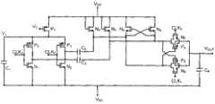
PMOS管P1~P5、NMOS管N1~N8、电容C1~C4,其中,P1的栅极接此高电压产生单元的输入端VJ,P1的源极接电源VDD,P1的漏极与P2的源极及衬底、P3的源极及衬底相接,并与C1的上极板连接在一起,C1的下极板接地VSS,P2、N1的栅极接第一时钟端CLK1,P3、N2的栅极接第二时钟端CLK2,P2、N1的漏极与C3的下极板相接,P3、N2的漏极与C2的下极板相接,N1、N2的源极接地VSS,N3的源极与N5的源极、N6的栅极、P4的栅极、P5的漏极、N8的漏极相接,并与C2的上极板连接在一起,N4的源极与N6的源极、N5的栅极、P5的栅极、P4的漏极、N7的漏极相接,并与C3的上极板连接在一起,N3的栅极、N3的漏极、N4的栅极、N4的漏极、N5的漏极、N6的漏极都接电源VDD,N7的栅极接第二时钟端CLK2,N8的栅极接第一时钟端CLK1,N7的源极与P4的源极、P4的衬底、P5的源极、P5的衬底、N8的源极相接,并与C4的上极板连接在一起,其连接点为此高电压产生单元的输出端,即整个电荷泵电路的输出端VOUT,C4的下极板接地VSS;和PMOS transistors P1 to P5 , NMOS transistors N1 to N8 , and capacitors C1 to C4 , where the gate of P1 is connected to the input terminal VJ of the high voltage generating unit, and the source of P1 is connected to the power supply VDD , the drain of P1 is connected to the source and substrate of P2 , the source and substrate of P3 , and connected to the upper plate of C1 , the lower plate of C1 is grounded VSS , The gates of P2 and N1 are connected to the first clock terminal CLK1 , the gates of P3 and N2 are connected to the second clock terminal CLK2 , the drains of P2 and N1 are connected to the lower plate of C3 , The drains of P3 and N2 are connected to the lower plate of C2 , the sources of N1 and N2 are grounded to VSS , the source of N3 is connected to the source of N5 , the gate of N6 , and the gate of P4 The gate of N4, the drain ofP5 , and the drain ofN8 are connected together, and connected with the upper plate ofC2 , the source ofN4 is connected with the source ofN6 , the gate ofN5 ,P5 The gate ofP4 , the drain ofN7 , and the upper plate ofC3 are connected together, the gate ofN3 , the drain ofN3 , the gate ofN4 , the gate of N4 The drain, the drain of N5 and the drain of N6 are all connected to the power supply VDD , the gate of N7 is connected to the second clock terminal CLK2 , the gate of N8 is connected to the first clock terminal CLK1 , and the source of N7 The pole is connected to the source ofP4 , the substrate ofP4 , the source ofP5 , the substrate ofP5 , and the source ofN8 , and is connected with the upper plate ofC4 , and its connection point is The output terminal of this high voltage generating unit, that is, the output terminal VOUT of the entire charge pump circuit, the lower plate of C4 is grounded VSS ; and
一个降压单元,包括:A step-down unit consisting of:
PMOS管P6~P7、NMOS管N9~N14、电容C5~C7,其中,N9的源极、P6的源极、P6的衬底、P7的源极、P7的衬底、N10的源极都与此降压单元的输入端,即高压产生单元的输出端VOUT相接,N9的漏极与P6的漏极、N11的漏极、N12的漏极、P7的栅极、N13的栅极相接,并与C5的上极板连接在一起,N10的漏极与P7的漏极、N13的漏极、N14的漏极、P6的栅极、N12的栅极相接,并与C6的上极板连接在一起,N9的栅极与C5的下极板、N14的栅极与第二时钟端CLK2相接,N10的栅极、C6的下极板、N11的栅极与第一时钟端CLK1相接,N11的源极与N12的源极、N13的源极、N14的源极相接,并与C7的上极板连接在一起,其连接点为此降压单元的输出端VFB,C7的下极板接地VSS;和PMOS transistors P6 to P7 , NMOS transistors N9 to N14 , and capacitors C5 to C7 , among which, the source of N9 , the source of P6 , the substrate of P6 , the source of P7 , and the The substrate of7 and the source of N10 are all connected to the input end of the step-down unit, that is, the output end VOUT of the high-voltage generating unit, and the drain of N9 is connected to the drain of P6 , the drain of N11 , The drain of N12 , the gate of P7 , and the gate of N13 are connected, and connected with the upper plate of C5 , the drain of N10 is connected with the drain of P7 , the drain of N13 , The drain of N14 , the gate of P6 , and the gate of N12 are connected, and connected with the upper plate of C6 , the gate of N9 is connected with the lower plate of C5 , and the gate of N14 It is connected to the second clock terminal CLK2 , the gate of N10 , the lower plate of C6 , the gate of N11 is connected to the first clock terminal CLK1 , the source of N11 is connected to the source of N12 , The source of N13 and the source of N14 are connected, and connected together with the upper plate of C7 , the connection point is the output terminal VFB of the step-down unit, and the lower plate of C7 is grounded VSS ; and
一个反馈控制单元,包括:A feedback control unit comprising:
PMOS管P8~P9、NMOS管N15~N18,其中,P8的源极、P9的源极接电源VDD,P8的栅极及漏极、P9的栅极与N5的漏极相接,P9的漏极与N16的漏极相接,其接点为此反馈控制单元的输出端VJ,即高压产生单元的输入端VJ,N15的栅极接此反馈控制单元的输入端,即降压单元的输出端VFB,N16的栅极接此反馈控制单元的输入VREF,N15的源极、N16的源极与N17的漏极相接,N17的栅极、N18的栅极、N18的漏极都与此反馈控制单元的输入端IBIAS相接,N17的源极、N18的源极均接地VSS。PMOS transistors P8 to P9 , NMOS transistors N15 to N18 , wherein the source of P8 and the source of P9 are connected to the power supply VDD , the gate and drain of P8 , the gate of P9 are connected to the N The drain of P9 is connected to the drain of N16 , and its contact point is the output terminal VJ of the feedback control unit, that is, theinput terminal VJ of the high-voltage generating unit, and the gate of N15 is connected to The input terminal of this feedback control unit, that is, the output terminal VFB of the step-down unit, the gate ofN16 is connected to the input VREF of this feedback control unit, the source ofN15 , the source ofN16 and the drain ofN17 The gate of N17 , the gate of N18 , and the drain of N18 are all connected to the input terminal IBIAS of the feedback control unit, and the source of N17 and N18 are both grounded to VSS .
所述电荷泵电路能够产生连续变化的输出电压值,且输出电压大于电源电压。The charge pump circuit can generate a continuously variable output voltage value, and the output voltage is greater than the power supply voltage.
所述电荷泵电路能够利用反馈功能来调节电荷泵的输出电压,使输出电压随输入电压的变化而变化。The charge pump circuit can use the feedback function to adjust the output voltage of the charge pump, so that the output voltage changes with the change of the input voltage.
所述电荷泵电路的电荷泵增益与MOS管的阈值电压无关。The charge pump gain of the charge pump circuit has nothing to do with the threshold voltage of the MOS tube.
所述电荷泵电路包含两个充电通路,在时钟的控制下,交替向负载充电。The charge pump circuit includes two charging paths, which alternately charge the load under the control of the clock.
有益效果:Beneficial effect:
本发明的基于反馈的电荷泵电路包括一个高电压产生单元、一个降压单元和一个反馈控制单元,与传统电荷泵电路相比,它具有以下特点:The charge pump circuit based on feedback of the present invention includes a high voltage generation unit, a step-down unit and a feedback control unit, compared with the traditional charge pump circuit, it has the following characteristics:
1.传统电荷泵电路只包含一个高压产生单元,而本发明的电荷泵电路在传统电荷泵电路基础上增加了一个降压单元和一个反馈控制单元,充分利用反馈的功能来调节电荷泵的输出电压。1. The traditional charge pump circuit only includes a high-voltage generating unit, but the charge pump circuit of the present invention adds a step-down unit and a feedback control unit on the basis of the traditional charge pump circuit, and makes full use of the feedback function to adjust the output of the charge pump Voltage.
2.传统电荷泵电路的电荷泵增益受阈值电压影响,导致其增压效率低,而本发明的电荷泵电路,其电荷泵增益与MOS管的阈值电压无关,能使增压效率提高20%以上。2. The charge pump gain of the traditional charge pump circuit is affected by the threshold voltage, resulting in low boosting efficiency, while the charge pump circuit of the present invention has nothing to do with the threshold voltage of the MOS tube, which can increase the boosting efficiency by 20% above.
3.传统电荷泵电路仅有一个充电通路,在时钟控制下,泵电容需要半个时钟周期预充电,再用半个时钟周期向负载充电,因此充电速度较慢,而本发明的电荷泵电路采用两个充电通路,交替向负载充电方式,使泵电容在整个时钟周期内都在向负载充电,再加上增压效率的提高,因此充电速度提高到两倍以上。3. The traditional charge pump circuit has only one charging path. Under clock control, the pump capacitor needs half a clock cycle to precharge, and then uses half a clock cycle to charge the load, so the charging speed is relatively slow, while the charge pump circuit of the present invention Two charging channels are used to charge the load alternately, so that the pump capacitor is charging the load during the entire clock cycle. In addition, the boosting efficiency is improved, so the charging speed is more than doubled.
4.传统电荷泵电路中,改变输出电压值通过改变电荷泵的级数实现,每级电荷泵增益固定,只能得到一些离散的电压值,因此其输出电压值不连续,而本发明的电荷泵电路,通过连续改变反馈控制单元的输入电压即可实现电荷泵输出电压的连续调节,因此可以得到一定范围内的任意输出电压值。4. In the traditional charge pump circuit, changing the output voltage value is achieved by changing the number of stages of the charge pump. The gain of each stage charge pump is fixed, and only some discrete voltage values can be obtained, so the output voltage value is discontinuous, and the charge pump of the present invention The pump circuit can continuously adjust the output voltage of the charge pump by continuously changing the input voltage of the feedback control unit, so any output voltage value within a certain range can be obtained.
综上所述,本发明的基于反馈的电荷泵电路同时具增压效率高、充电速度快、输出电压值连续的优点,有效克服了传统电荷泵电路的增压效率低、输出电压值离散、充电速度慢的缺点。In summary, the feedback-based charge pump circuit of the present invention has the advantages of high boosting efficiency, fast charging speed, and continuous output voltage value at the same time, effectively overcoming the low boosting efficiency, discrete output voltage value, and The disadvantage of slow charging.
附图说明Description of drawings
图1是本发明的基于反馈的电荷泵电路的总体电路框图;Fig. 1 is the general circuit block diagram of the charge pump circuit based on feedback of the present invention;
图2是本发明图1中的高电压产生单元的电路图;Fig. 2 is the circuit diagram of the high voltage generating unit in Fig. 1 of the present invention;
图3是本发明图1中的降压单元的电路图;Fig. 3 is a circuit diagram of the step-down unit in Fig. 1 of the present invention;
图4是本发明图1中的反馈控制单元的电路图。FIG. 4 is a circuit diagram of the feedback control unit in FIG. 1 of the present invention.
具体实施方式Detailed ways
本发明的具体实施方式不仅限于下面的描述,现结合附图加以进一步说明。The specific implementation manners of the present invention are not limited to the following description, and are now further described in conjunction with the accompanying drawings.
本发明具体实施的一种基于反馈的电荷泵电路总体结构如图1所示。它由一个高压产生单元、一个降压单元和一个反馈控制单元组成。其中,高压产生单元的电路图如图2所示,包括:PMOS管P1~P5、NMOS管N1~N8、电容C1~C4,高压产生单元用于产生大于电源电压的高电压。降压单元的电路图如图3所示,包括:PMOS管P6~P7、NMOS管N9~N14、电容C5~C7,降压单元将高电压降低到电源电压范围内,以便于反馈控制单元进行比较反馈。反馈控制单元的电路图如图4所示,包括PMOS管P8~P9、NMOS管N15~N18,反馈控制单元将输出电压经降压后的值与输入电压进行比较,比较的结果用于控制高压产生电路,实现对电荷泵电路输出高电压的反馈控制。The overall structure of a feedback-based charge pump circuit implemented in the present invention is shown in FIG. 1 . It consists of a high-voltage generating unit, a step-down unit and a feedback control unit. Among them, the circuit diagram of the high-voltage generating unit is shown in Figure 2, including: PMOS transistors P1 to P5 , NMOS transistors N1 to N8 , capacitors C1 to C4 , and the high-voltage generating unit is used to generate a high voltage greater than the power supply voltage . The circuit diagram of the step-down unit is shown in Figure 3, including: PMOS transistors P6 to P7 , NMOS transistors N9 to N14 , capacitors C5 to C7 , and the step-down unit reduces the high voltage to the power supply voltage range, so that The comparative feedback is carried out in the feedback control unit. The circuit diagram of the feedback control unit is shown in Figure 4, including PMOS transistors P8 to P9 and NMOS transistors N15 to N18 . The feedback control unit compares the output voltage after step-down with the input voltage, and the comparison result is used It is used to control the high-voltage generating circuit and realize the feedback control of the output high voltage of the charge pump circuit.
图2中的具体连接关系与本说明书的发明内容部分相同,此处不再重复。它的工作原理如下:The specific connection relationship in FIG. 2 is the same as the content of the invention in this specification, and will not be repeated here. It works like this:
时钟CLK1和CLK2为两相非交叠时钟,当CLK1为高电平、CLK2为低电平时,N1导通,C3底极板接地,N4或N6为C3充电(初态时N4为C3充电,稳态时,N6为C3充电),稳态时C3上极板充电到VDD 当CLK1为低电平、CLK2为高电平时,P2导通,C3底极板与C1上极板相连(C1上极板电压稳态时为V1),因此由C3上极板节点电荷守恒,可得稳态时C3上极板电压被举高到:Clocks CLK1 and CLK2 are two-phase non-overlapping clocks. When CLK1 is high and CLK2 is low, N1 is turned on, the bottom plate of C3 is grounded, and N4 or N6 charges C3 (N4 charges C3 in the initial state, and N6 charges C3 in the steady state). In the steady state, the upper plate of C3 is charged to VDD . When CLK1 is low and CLK2 is high, P2 is turned on, and the bottom plate of C3 is connected to the upper plate of C1 (the voltage of the upper plate of C1 is V1 in a steady state), so the charge conservation of the upper plate node of C3 can get C3 in a steady state The upper plate voltage is raised to:
式中,CP3为C3上极板节点的寄生电容。In the formula, CP3 is the parasitic capacitance of the plate node on C3 .
同理,当CLK1为低电平、CLK2为高电平时,稳态时C2上极板充电到VDD;当CLK1为高电平、CLK2为低电平时,稳态时C2上极板电压被举高到:Similarly, when CLK1 is low level and CLK2 is high level, the upper plate of C2 is charged to VDD in steady state; when CLK1 is high level and CLK2 is low level, C2 The upper plate voltage is raised to:
式中,CP2为C2上极板节点的寄生电容。In the formula, CP2 is the parasitic capacitance of the plate node on C2 .
由于电路采用对称设计,因此Due to the symmetrical design of the circuit, the
C2=C3=C2,3 (5)C2 =C3 =C2,3 (5)
Cp2=Cp3=Cp2,3 (6)Cp2 =Cp3 =Cp2,3 (6)
有(3)~(6)式可得:There are formulas (3)~(6) to get:
V3=V2=VDD+ΔV1 (7)V3 =V2 =VDD +ΔV1 (7)
其中,
若like
ΔV1>|Vthp| (9)ΔV1 > |Vthp | (9)
式中,Vthp为PMOS晶体管的阈值电压。Where, Vthp is the threshold voltage of the PMOS transistor.
当CLK1为高电平、CLK2为低电平时,初态时,P4、P5、N7截止,N8导通,C2向C4充电;稳态时,由于C2上极板电压被举高到(VDD+ΔV1),C3上极板电压为VDD,由(9)式可知,P4、N7、N8截止,P5导通,C2将C4上极板充电到(VDD+ΔV1)。当CLK1为低电平、CLK2为高电平时,初态时,P4、P5、N8截止,N7导通,C3向C4充电;稳态时,由于C3上极板电压被举高到(VDD+ΔV1),C2上极板电压为VDD,由(9)式可知,P5、N7、N8截止,P4导通,C3将C4上极板充电到(VDD+ΔV1)。可见,在时钟CLK1和CLK2的控制下,C2和C3交替的向C4充电,最终使C4上极板电压,即输出电压达到以下稳定值:When CLK1 is at high level and CLK2 is at low level, in the initial state, P4 , P5 , and N7 are turned off, N8 is turned on, and C2 charges to C4 ; in steady state, due to the upper pole of C2 The plate voltage is raised to (VDD +ΔV1 ), and the plate voltage on C3 is VDD . It can be seen from formula (9) that P4 , N7 , and N8 are cut off, P5 is turned on, and C2 turns C4 The upper plate is charged to (VDD +ΔV1 ). When CLK1 is at low level and CLK2 is at high level, in the initial state, P4 , P5 , and N8 are turned off, N7 is turned on, and C3 charges to C4 ; in steady state, due to the upper pole of C3 The plate voltage is raised to (VDD +ΔV1 ), and the plate voltage on C2 is VDD . It can be seen from formula (9) that P5 , N7 , and N8 are off, P4 is on, and C3 turns C4 The upper plate is charged to (VDD +ΔV1 ). It can be seen that under the control of clock CLK1 and CLK2 , C2 and C3 charge C4 alternately, and finally make the upper plate voltage of C4 , that is, the output voltage reach the following stable value:
VOUT=VDD+ΔV1 (10)VOUT =VDD +ΔV1 (10)
图3中的具体连接关系与本说明书的发明内容部分相同,此处不再重复。它的工作原理如下:The specific connection relationship in FIG. 3 is the same as the content of the invention in this specification, and will not be repeated here. It works like this:
当CLK1为高电平、CLK2为低电平时,初态时,P6、P7、N9截止,N10导通,VOUT向C6充电,N12、N13、N14截止,N11导通,C5向C7充电;稳态时,P6、N9、N10截止,P7导通,N11、N13、N14截止,N12导通。此时,C6上极板电压为VOUT,由C5上极板节点电荷守恒,可得C5上极板电压为:When CLK1 is at high level and CLK2 is at low level, in the initial state, P6 , P7 , and N9 are off, N10 is on, VOUT charges C6 , and N12 , N13 , and N14 are off , N11 is turned on, C5 charges C7 ; in steady state, P6 , N9 , N10 are turned off, P7 is turned on, N11 , N13 , N14 are turned off, and N12 is turned on. At this time, the voltage of the upper plate of C6 is VOUT , and the charge conservation of the node of the upper plate of C5 can obtain the voltage of the upper plate of C5 as:
式中,CP5为C5上极板节点的寄生电容,此时,C5将C7上极板充电到V5。In the formula, CP5 is the parasitic capacitance of the upper plate node of C5 , at this time, C5 charges the upper plate of C7 to V5 .
当CLK1为低电平、CLK2为高电平时,初态时,P6、P7、N10截止,N9导通,VOUT向C5充电,N11、N12、N13截止,N14导通,C6向C7充电;稳态时,P7、N9、N10截止,P6导通,N11、N12、N14截止,N13导通。此时,C5上极板电压为VOUT,由C6上极板节点电荷守恒,可得C6上极板电压为:When CLK1 is at low level and CLK2 is at high level, in the initial state, P6 , P7 , and N10 are off, N9 is on, VOUT charges C5 , and N11 , N12 , and N13 are off , N14 is turned on, C6 charges to C7 ; in steady state, P7 , N9 , N10 are turned off, P6 is turned on, N11 , N12 , N14 are turned off, and N13 is turned on. At this time, the voltage of the upper plate of C5 is VOUT , and the charge conservation of the upper plate node of C6 can obtain the voltage of the upper plate of C6 as:
式中,CP6为C6上极板节点的寄生电容,此时,C6将C7上极板充电到V6。In the formula, CP6 is the parasitic capacitance of the upper plate node of C6 , at this time, C6 charges the upper plate of C7 to V6 .
由于电路采用对称设计,因此有:Since the circuit is designed symmetrically, there are:
C5=C6=C5,6 (13)C5 =C6 =C5,6 (13)
Cp5=Cp6=Cp5,6 (14)Cp5 =Cp6 =Cp5,6 (14)
由(11)~(14)式,可得:From formulas (11) to (14), we can get:
V5=V6=VOUT-ΔV2 (15)V5 =V6 =VOUT -ΔV2 (15)
式中,
可见,C5与C6在时钟控制下,交替的被VOUT充电,并向C7充电,得到VOUT经降压后的值:It can be seen that under clock control, C5 and C6 are alternately charged by VOUT and charged to C7 to obtain the value of VOUT after step-down:
VFB=V5=V6=VOUT-ΔV2 (17)VFB =V5 =V6 =VOUT -ΔV2 (17)
图4中的具体连接关系与本说明书的发明内容部分相同,此处不再重复。它的工作原理如下:The specific connection relationship in FIG. 4 is the same as the content of the invention in this specification, and will not be repeated here. It works like this:
IBIAS为偏置电流输入端,通过N18向N17的镜像,为运放提供偏置,VREF为输入电压。当VFB小于VREF时,VJ减小,使图2中V1升高,由(8)和(10)式可知,稳态时,VOUT将升高;当VFB大于VREF时,VJ增大,使图2中V1降低,由(8)和式(10)式可知,稳态时VOUT将降低;直到VFB等于VREF时,VOUT达到稳态平衡,由(16)和(17)式可知,此时,IBIAS is the input terminal of the bias current, through the mirror image of N18 to N17 , it provides bias for the operational amplifier, and VREF is the input voltage. When VFB is less than VREF , VJ decreases, which increases V1 in Figure 2. It can be seen from (8) and (10) that in steady state, VOUT will increase; when VFB is greater than VREF , VJ increases, so that V1 in Figure 2 decreases. It can be seen from (8) and (10) that VOUT will decrease in the steady state; until VFB is equal to VREF , VOUT will reach a steady state balance. (16) and (17), it can be seen that at this time,
综上所述,首先,对比(1)式和(8)式可知,电荷泵增益ΔV1与NMOS管的阈值电压无关,且当泵节点的电压变化V1=VDD时,本发明电路的电荷泵增益ΔV1较之传统电荷泵电路的电荷泵增益ΔV,增大了一个阈值电压值Vthn,若C2,3远大于Cp2,3,则电荷泵增益约为泵节点电压变化的100%;其次,由式(18)可知,由于引入了反馈,使得连续改变VREF可使VOUT随之连续改变,因此,本发明电路的电路结构避免了传统电荷泵电路的输出电压不能连续调节的问题;同时,本发明电路采用了双通路交替的方式,满时钟周期连续地向负载充电,再加上电荷泵增益的提高,充电速度提高到传统电荷泵电路的2倍以上。In summary, first of all, comparing formula (1) and formula (8), it can be seen that the charge pump gain ΔV1 has nothing to do with the threshold voltage of the NMOS transistor, and when the voltage change of the pump node V1 =VDD , the circuit of the present invention Compared with the charge pump gain ΔV of the traditional charge pump circuit, the charge pump gain ΔV1 increases a threshold voltage value Vthn , if C2,3 is much larger than Cp2,3 , then the charge pump gain is about 100%; secondly, by the formula (18), it can be known that due to the introduction of feedback, continuously changing VREF can make VOUT continuously change thereupon, therefore, the circuit structure of the circuit of the present invention has avoided the output voltage of the traditional charge pump circuit can not be continuous The problem of regulation; at the same time, the circuit of the present invention adopts the dual-channel alternate mode, and the full clock cycle continuously charges the load, coupled with the improvement of the charge pump gain, the charging speed is increased to more than 2 times that of the traditional charge pump circuit.
另外,为了进一步提高工作速度,本发明的充放电通路上的MOS管,即P2~P7,N1~N14都采用最小的栅长。为实现对输出电压VOUT的连续充电和连续采样反馈,使C2、C3对C4的交替充电,C5、C6对VOUT的交替采样和降压,本发明电路采用对称设计,即P2、P3几何尺寸完全相同,N1、N2几何尺寸完全相同,C2、C3几何尺寸完全相同,N3、N4几何尺寸完全相同,N5、N6几何尺寸完全相同,N7、N8几何尺寸完全相同,P4、P5几何尺寸完全相同,N9、N10几何尺寸完全相同,P6、P7几何尺寸完全相同,N11、N14几何尺寸完全相同,N12、N13几何尺寸完全相同,P8、P9几何尺寸完全相同,N15、N16几何尺寸完全相同,N17和N18沟道长度相同,宽度成比例。In addition, in order to further increase the working speed, the MOS transistors on the charging and discharging path of the present invention, that is, P2 -P7 , N1 -N14 all adopt the minimum gate length. In order to realize the continuous charging and continuous sampling feedback of the output voltage VOUT , so that C2 and C3 can charge C4 alternately, and C5 and C6 can alternately sample and step down VOUT , the circuit of the present invention adopts a symmetrical design, That is, the geometric dimensions of P2 and P3 are identical, the geometric dimensions of N1 and N2 are identical, the geometric dimensions of C2 and C3 are identical, the geometric dimensions of N3 and N4 are identical, and the geometric dimensions of N5 and N6 are identical , the geometric dimensions of N7 and N8 are identical, the geometric dimensions of P4 and P5 are identical, the geometric dimensions of N9 and N10 are identical, the geometric dimensions of P6 and P7 are identical, and the geometric dimensions of N11 and N14 are identical , N12 and N13 have the same geometric dimensions, P8 and P9 have the same geometric dimensions, N15 and N16 have the same geometric dimensions, N17 and N18 have the same channel length and proportional width.
本发明的制造工艺为通用的硅栅N阱CMOS工艺。The manufacturing process of the present invention is a common silicon gate N well CMOS process.
本发明电路中的PMOS、NMOS管的基本参数为:The basic parameters of PMOS and NMOS tubes in the circuit of the present invention are:
NMOS管的阈值电压Vthn:0.6~0.8V;Threshold voltage Vthn of NMOS transistor: 0.6~0.8V;
PMOS管的阈值电压Vthp:-0.6~-0.8V;Threshold voltage Vthp of PMOS transistor: -0.6~-0.8V;
输入电压VREF>1V。The input voltage VREF >1V.
Claims (5)
Translated fromChinesePriority Applications (1)
| Application Number | Priority Date | Filing Date | Title |
|---|---|---|---|
| CN2010102423182ACN101888181B (en) | 2010-08-02 | 2010-08-02 | Charge pump circuit based on feedback |
Applications Claiming Priority (1)
| Application Number | Priority Date | Filing Date | Title |
|---|---|---|---|
| CN2010102423182ACN101888181B (en) | 2010-08-02 | 2010-08-02 | Charge pump circuit based on feedback |
Publications (2)
| Publication Number | Publication Date |
|---|---|
| CN101888181Atrue CN101888181A (en) | 2010-11-17 |
| CN101888181B CN101888181B (en) | 2012-09-05 |
Family
ID=43073942
Family Applications (1)
| Application Number | Title | Priority Date | Filing Date |
|---|---|---|---|
| CN2010102423182AExpired - Fee RelatedCN101888181B (en) | 2010-08-02 | 2010-08-02 | Charge pump circuit based on feedback |
Country Status (1)
| Country | Link |
|---|---|
| CN (1) | CN101888181B (en) |
Cited By (8)
| Publication number | Priority date | Publication date | Assignee | Title |
|---|---|---|---|---|
| CN103312162A (en)* | 2012-03-08 | 2013-09-18 | 扬州稻源微电子有限公司 | Voltage doubler circuit and radio frequency identification label chip comprising voltage doubler circuit |
| CN104714589A (en)* | 2015-01-09 | 2015-06-17 | 中国电子科技集团公司第二十四研究所 | CMOS on-chip direct-current negative voltage generation circuit |
| CN105048801A (en)* | 2015-08-24 | 2015-11-11 | 北京兆易创新科技股份有限公司 | Voltage conversion circuit |
| CN105043435A (en)* | 2014-04-30 | 2015-11-11 | 英飞凌科技股份有限公司 | Systems and methods for high voltage bridge bias generation and low voltage readout circuitry |
| CN107070203A (en)* | 2017-04-21 | 2017-08-18 | 成都锐成芯微科技股份有限公司 | Differential charge pump element circuit |
| CN107453599A (en)* | 2017-07-17 | 2017-12-08 | 上海华虹宏力半导体制造有限公司 | The malleation charge pump of multivoltage output |
| CN108227807A (en)* | 2017-12-29 | 2018-06-29 | 深圳市华星光电技术有限公司 | A kind of voltage control circuit, display and voltage control method |
| CN109756107A (en)* | 2019-01-31 | 2019-05-14 | 深圳市爱协生科技有限公司 | A high-efficiency charge pump circuit structure |
Citations (6)
| Publication number | Priority date | Publication date | Assignee | Title |
|---|---|---|---|---|
| US20020060591A1 (en)* | 2000-11-20 | 2002-05-23 | Yoshiaki Ito | Phase-locked loop circuit outputting clock signal having fixed phase difference with respect to input clock signal |
| CN1882895A (en)* | 2003-10-07 | 2006-12-20 | 爱特梅尔股份有限公司 | High precision digital-to-analog converter with optimized power consumption |
| US20070211502A1 (en)* | 2006-03-07 | 2007-09-13 | Kunihiro Komiya | Voltage step-up circuit and electric appliance therewith |
| CN101116248A (en)* | 2004-12-13 | 2008-01-30 | 睦塞德技术公司 | Phase locked loop circuit using charge pump with current mirror circuit |
| US20090121759A1 (en)* | 2007-11-13 | 2009-05-14 | Qualcomm Incorporated | Fast-switching low-noise charge pump |
| CN101674009A (en)* | 2008-09-10 | 2010-03-17 | 中芯国际集成电路制造(上海)有限公司 | Charge pump output voltage regulation circuit |
- 2010
- 2010-08-02CNCN2010102423182Apatent/CN101888181B/ennot_activeExpired - Fee Related
Patent Citations (6)
| Publication number | Priority date | Publication date | Assignee | Title |
|---|---|---|---|---|
| US20020060591A1 (en)* | 2000-11-20 | 2002-05-23 | Yoshiaki Ito | Phase-locked loop circuit outputting clock signal having fixed phase difference with respect to input clock signal |
| CN1882895A (en)* | 2003-10-07 | 2006-12-20 | 爱特梅尔股份有限公司 | High precision digital-to-analog converter with optimized power consumption |
| CN101116248A (en)* | 2004-12-13 | 2008-01-30 | 睦塞德技术公司 | Phase locked loop circuit using charge pump with current mirror circuit |
| US20070211502A1 (en)* | 2006-03-07 | 2007-09-13 | Kunihiro Komiya | Voltage step-up circuit and electric appliance therewith |
| US20090121759A1 (en)* | 2007-11-13 | 2009-05-14 | Qualcomm Incorporated | Fast-switching low-noise charge pump |
| CN101674009A (en)* | 2008-09-10 | 2010-03-17 | 中芯国际集成电路制造(上海)有限公司 | Charge pump output voltage regulation circuit |
Non-Patent Citations (1)
| Title |
|---|
| 《华中科技大学学报(自然科学版)》 20050228 彭颖等 一种用于锁相环的正反馈互补型电荷泵电路 第33卷, 第2期* |
Cited By (14)
| Publication number | Priority date | Publication date | Assignee | Title |
|---|---|---|---|---|
| CN103312162A (en)* | 2012-03-08 | 2013-09-18 | 扬州稻源微电子有限公司 | Voltage doubler circuit and radio frequency identification label chip comprising voltage doubler circuit |
| CN103312162B (en)* | 2012-03-08 | 2016-01-13 | 扬州稻源微电子有限公司 | Voltage-multiplying circuit and comprise its radio frequency identification label chip |
| CN105043435B (en)* | 2014-04-30 | 2017-12-19 | 英飞凌科技股份有限公司 | For high voltage bridge biasing generation and the system and method for low-voltage reading circuit |
| CN105043435A (en)* | 2014-04-30 | 2015-11-11 | 英飞凌科技股份有限公司 | Systems and methods for high voltage bridge bias generation and low voltage readout circuitry |
| US9921249B2 (en) | 2014-04-30 | 2018-03-20 | Infineon Technologies Ag | Systems and methods for high voltage bridge bias generation and low voltage readout circuitry |
| CN104714589A (en)* | 2015-01-09 | 2015-06-17 | 中国电子科技集团公司第二十四研究所 | CMOS on-chip direct-current negative voltage generation circuit |
| CN105048801B (en)* | 2015-08-24 | 2018-04-17 | 北京兆易创新科技股份有限公司 | A kind of voltage conversion circuit |
| CN105048801A (en)* | 2015-08-24 | 2015-11-11 | 北京兆易创新科技股份有限公司 | Voltage conversion circuit |
| CN107070203A (en)* | 2017-04-21 | 2017-08-18 | 成都锐成芯微科技股份有限公司 | Differential charge pump element circuit |
| CN107453599A (en)* | 2017-07-17 | 2017-12-08 | 上海华虹宏力半导体制造有限公司 | The malleation charge pump of multivoltage output |
| CN107453599B (en)* | 2017-07-17 | 2020-02-07 | 上海华虹宏力半导体制造有限公司 | Multi-voltage output positive-voltage charge pump |
| CN108227807A (en)* | 2017-12-29 | 2018-06-29 | 深圳市华星光电技术有限公司 | A kind of voltage control circuit, display and voltage control method |
| WO2019127687A1 (en)* | 2017-12-29 | 2019-07-04 | 深圳市华星光电技术有限公司 | Voltage control circuit, display device, and voltage control method |
| CN109756107A (en)* | 2019-01-31 | 2019-05-14 | 深圳市爱协生科技有限公司 | A high-efficiency charge pump circuit structure |
Also Published As
| Publication number | Publication date |
|---|---|
| CN101888181B (en) | 2012-09-05 |
Similar Documents
| Publication | Publication Date | Title |
|---|---|---|
| CN101888181B (en) | Charge pump circuit based on feedback | |
| US7893778B2 (en) | Flexible low current oscillator for multiphase operations | |
| CN108508951B (en) | LDO voltage regulator circuit without off-chip capacitor | |
| US8339118B2 (en) | Adaptive bias current generator methods and apparatus | |
| CN106655757B (en) | Capacitive charge pump | |
| CN108574410A (en) | Circuit and method for realizing fast and high-precision adaptive slope compensation | |
| CN107070202A (en) | Circuit for generating negative voltage with voltage automatic regulation function | |
| CN111509973B (en) | Charge pump capable of reducing output voltage ripple | |
| CN102005917B (en) | Constant voltage output charge pump circuit | |
| CN106712495A (en) | Charge pump circuit | |
| CN102386893A (en) | Adjustable square signal generation circuit and switch-type regulator utilizing same | |
| CN101272090B (en) | High tension charge pump circuit | |
| CN103592989B (en) | The OCL output capacitance-less LDO circuit of low speed paper tape reader static power disspation fast transient response | |
| CN104143907B (en) | Double-ring charge pump control circuit for discontinuous current control | |
| JP2012075092A (en) | Oscillation circuit and semiconductor device including the same | |
| CN108809084A (en) | Charge pump circuit | |
| CN114744869B (en) | Three-level step-down direct current converter | |
| CN217545877U (en) | Negative-pressure charge pump and radio frequency switch chip | |
| CN101106323A (en) | A low voltage, high gain charge pump circuit | |
| CN103279162B (en) | Low-power-consumption reference voltage buffer based on assembly line ADC | |
| CN109639135B (en) | Charge pump circuit | |
| CN107395012B (en) | A charge pump circuit and its control method | |
| CN205544931U (en) | System for substrate bias circuit, voltage multiplier and contain said voltage multiplier | |
| CN106787712A (en) | A kind of premodulated capacitor type direct current transducer based on capacitor array conversion | |
| US9866111B1 (en) | Regulated charge pump circuit |
Legal Events
| Date | Code | Title | Description |
|---|---|---|---|
| C06 | Publication | ||
| PB01 | Publication | ||
| C10 | Entry into substantive examination | ||
| SE01 | Entry into force of request for substantive examination | ||
| C14 | Grant of patent or utility model | ||
| GR01 | Patent grant | ||
| C17 | Cessation of patent right | ||
| CF01 | Termination of patent right due to non-payment of annual fee | Granted publication date:20120905 Termination date:20130802 |