CN101887134A - A kind of infrared window protective film material, its application and preparation method - Google Patents
A kind of infrared window protective film material, its application and preparation methodDownload PDFInfo
- Publication number
- CN101887134A CN101887134ACN2010101955098ACN201010195509ACN101887134ACN 101887134 ACN101887134 ACN 101887134ACN 2010101955098 ACN2010101955098 ACN 2010101955098ACN 201010195509 ACN201010195509 ACN 201010195509ACN 101887134 ACN101887134 ACN 101887134A
- Authority
- CN
- China
- Prior art keywords
- protective film
- deposition
- substrate
- infrared
- reaction chamber
- Prior art date
- Legal status (The legal status is an assumption and is not a legal conclusion. Google has not performed a legal analysis and makes no representation as to the accuracy of the status listed.)
- Pending
Links
- 239000000463materialSubstances0.000titleclaimsabstractdescription31
- 230000001681protective effectEffects0.000titleclaimsabstractdescription29
- 238000002360preparation methodMethods0.000titleclaimsabstractdescription14
- 229910052735hafniumInorganic materials0.000claimsabstractdescription35
- 229910052726zirconiumInorganic materials0.000claimsabstractdescription35
- 150000004767nitridesChemical class0.000claimsabstractdescription26
- 230000003287optical effectEffects0.000claimsabstractdescription26
- SBIBMFFZSBJNJF-UHFFFAOYSA-Nselenium;zincChemical compound[Se]=[Zn]SBIBMFFZSBJNJF-UHFFFAOYSA-N0.000claimsabstractdescription25
- 238000000151depositionMethods0.000claimsabstractdescription21
- 230000008021depositionEffects0.000claimsabstractdescription21
- 238000000034methodMethods0.000claimsabstractdescription21
- IJGRMHOSHXDMSA-UHFFFAOYSA-NAtomic nitrogenChemical compoundN#NIJGRMHOSHXDMSA-UHFFFAOYSA-N0.000claimsabstractdescription16
- 229910052757nitrogenInorganic materials0.000claimsabstractdescription7
- 239000000758substrateSubstances0.000claimsdescription25
- 238000006243chemical reactionMethods0.000claimsdescription19
- XKRFYHLGVUSROY-UHFFFAOYSA-NArgonChemical compound[Ar]XKRFYHLGVUSROY-UHFFFAOYSA-N0.000claimsdescription12
- 239000007789gasSubstances0.000claimsdescription11
- 238000004544sputter depositionMethods0.000claimsdescription11
- 229910052723transition metalInorganic materials0.000claimsdescription11
- 150000003624transition metalsChemical class0.000claimsdescription11
- KPZGRMZPZLOPBS-UHFFFAOYSA-N1,3-dichloro-2,2-bis(chloromethyl)propaneChemical compoundClCC(CCl)(CCl)CClKPZGRMZPZLOPBS-UHFFFAOYSA-N0.000claimsdescription6
- 229910052786argonInorganic materials0.000claimsdescription6
- 238000005229chemical vapour depositionMethods0.000claimsdescription5
- 238000005530etchingMethods0.000claimsdescription4
- QGZKDVFQNNGYKY-UHFFFAOYSA-NAmmoniaChemical compoundNQGZKDVFQNNGYKY-UHFFFAOYSA-N0.000claimsdescription3
- 238000005137deposition processMethods0.000claimsdescription3
- 238000005516engineering processMethods0.000claimsdescription3
- 238000001755magnetron sputter depositionMethods0.000claimsdescription2
- 239000012495reaction gasSubstances0.000claimsdescription2
- 239000010408filmSubstances0.000abstractdescription53
- 239000010409thin filmSubstances0.000abstractdescription19
- 239000002184metalSubstances0.000abstract2
- 229910052751metalInorganic materials0.000abstract2
- 238000004519manufacturing processMethods0.000abstract1
- 239000000126substanceSubstances0.000abstract1
- 238000002834transmittanceMethods0.000description10
- 239000010432diamondSubstances0.000description5
- 229910003460diamondInorganic materials0.000description5
- 229910005742Ge—CInorganic materials0.000description2
- XYFCBTPGUUZFHI-UHFFFAOYSA-NPhosphineChemical compoundPXYFCBTPGUUZFHI-UHFFFAOYSA-N0.000description2
- 238000002441X-ray diffractionMethods0.000description2
- 229910008328ZrNxInorganic materials0.000description2
- UORVGPXVDQYIDP-UHFFFAOYSA-NboraneChemical compoundBUORVGPXVDQYIDP-UHFFFAOYSA-N0.000description2
- 238000010586diagramMethods0.000description2
- 229910001873dinitrogenInorganic materials0.000description2
- 238000006073displacement reactionMethods0.000description2
- 230000002349favourable effectEffects0.000description2
- 238000011056performance testMethods0.000description2
- 238000005240physical vapour depositionMethods0.000description2
- 238000000623plasma-assisted chemical vapour depositionMethods0.000description2
- 239000011241protective layerSubstances0.000description2
- 238000004458analytical methodMethods0.000description1
- 229910000085boraneInorganic materials0.000description1
- 239000011248coating agentSubstances0.000description1
- 238000000576coating methodMethods0.000description1
- 239000010410layerSubstances0.000description1
- 239000012788optical filmSubstances0.000description1
- 229910000073phosphorus hydrideInorganic materials0.000description1
- 230000035939shockEffects0.000description1
- 230000003595spectral effectEffects0.000description1
- 231100000331toxicToxicity0.000description1
- 230000002588toxic effectEffects0.000description1
- XLYOFNOQVPJJNP-UHFFFAOYSA-NwaterSubstancesOXLYOFNOQVPJJNP-UHFFFAOYSA-N0.000description1
Images

Landscapes
- Physical Vapour Deposition (AREA)
Abstract
Description
Translated fromChinese技术领域technical field
本发明属于红外光学薄膜技术领域,具体涉及一种新型的过渡族金属Zr、Hf的氮化物光学薄膜和其应用以及其制备方法。The invention belongs to the technical field of infrared optical thin films, and in particular relates to a novel transition metal Zr, Hf nitride optical thin film, its application and its preparation method.
背景技术Background technique
能够被应用在8~12μm远红外波段的光学材料的种类极为有限,而在有限的几种材料之中,ZnS、ZnSe是应用得最多的两种材料。ZnS、ZnSe在8~12μm波段具有很好的光学性能,但是,它们同时也有着很显著的缺点,其中,极低的硬度使ZnS、ZnSe在应用中很容易被划伤,从而导致其光学窗口的失效。The types of optical materials that can be applied in the 8-12 μm far-infrared band are extremely limited, and among the limited materials, ZnS and ZnSe are the two most widely used materials. ZnS and ZnSe have good optical properties in the 8-12 μm band, but they also have significant disadvantages. Among them, the extremely low hardness makes ZnS and ZnSe easy to be scratched in the application, resulting in their optical windows. failure.
到目前为止,人们已经研究了多种的ZnS、ZnSe保护层材料,其中包括类金刚石膜和Ge-C薄膜、PB薄膜以及金刚石薄膜等。作为ZnS、ZnSe窗口的保护膜来说,类金刚石膜和Ge-C薄膜具有一定的硬度,但是这种薄膜的应力太大,因而很难在ZnS、ZnSe窗口上涂敷较厚的类金刚石膜,因此类金刚石膜对ZnS、ZnSe窗口的保护作用有限(Waddell,Ewan M;Gibson,Desmond R;Meredith,J.Proceedings of SPIE-The International Society for Optical Engineering,v 2286,p 364-375,1994)。金刚石薄膜本身有极高的硬度,被认为是红外窗口最好的保护膜材料,但是金刚石膜的沉积条件过于苛刻,因而很难在ZnS、ZnSe窗口上制备出有足够面积、附着力足够好的金刚石保护膜(Moller A J,ReeceD M,Hudson M D.Diamond and Related Materials,1997,6:386)。PB薄膜是到目前为止用于ZnS、ZnSe窗口的最好的保护膜材料,但是制备PB薄膜需要使用毒性极大的磷烷与硼烷,因而PB的应用也较为有限(Clark,C.C.1;Haddow,D.1 Source:Proceedings of the SPIE-The International Societyfor Optical Engineering,v 4375,307-14,2001)。因此,寻找一种能够应用于ZnS、ZnSe红外光学窗口的保护膜材料具有很高的实际价值。So far, people have studied a variety of ZnS, ZnSe protective layer materials, including diamond-like film and Ge-C film, PB film and diamond film and so on. As the protective film of ZnS and ZnSe windows, diamond-like film and Ge-C film have certain hardness, but the stress of this film is too large, so it is difficult to coat thicker diamond-like film on ZnS and ZnSe window , so the diamond-like film has a limited protective effect on ZnS and ZnSe windows (Waddell, Ewan M; Gibson, Desmond R; Meredith, J.Proceedings of SPIE-The International Society for Optical Engineering, v 2286, p 364-375, 1994) . The diamond film itself has extremely high hardness and is considered to be the best protective film material for the infrared window. However, the deposition conditions of the diamond film are too harsh, so it is difficult to prepare a film with sufficient area and good adhesion on the ZnS and ZnSe windows. Diamond protective film (Moller A J, Reece D M, Hudson M D. Diamond and Related Materials, 1997, 6: 386). PB film is the best protective film material used for ZnS and ZnSe windows so far, but the preparation of PB film requires the use of extremely toxic phosphine and borane, so the application of PB is also relatively limited (Clark, C.C.1; Haddow , D.1 Source: Proceedings of the SPIE-The International Society for Optical Engineering, v 4375, 307-14, 2001). Therefore, it is of high practical value to find a protective film material that can be applied to ZnS and ZnSe infrared optical windows.
为了满足ZnS、ZnSe红外光学窗口对保护膜材料的迫切需求,本发明提出了一种可被用于制作远红外波段ZnS、ZnSe光学窗口保护膜的过渡金属Zr、Hf的氮化物材料和其制备方法,该保护膜可对ZnS、ZnSe等常用的红外光学窗口提供有效的保护。In order to meet the urgent needs of ZnS and ZnSe infrared optical windows for protective film materials, the present invention proposes a nitride material of transition metal Zr and Hf that can be used to make far-infrared band ZnS and ZnSe optical window protective films and its preparation method, the protective film can provide effective protection for commonly used infrared optical windows such as ZnS and ZnSe.
发明内容Contents of the invention
本发明的目的是为在8~12μm波段应用的红外光学窗口,尤其是ZnS、ZnSe光学窗口提供一种具有高透过率、同时具有高硬度和低内应力的新型保护膜材料。The purpose of the present invention is to provide a new type of protective film material with high transmittance, high hardness and low internal stress for infrared optical windows applied in the 8-12 μm wave band, especially ZnS and ZnSe optical windows.
本发明一种红外窗口保护膜材料,所述材料由过渡族金属Zr、Hf的氮化物所组成,成分为(Zr,Hf)Nx,其中x代表氮含量的数值。The invention relates to an infrared window protective film material, which is composed of transition metals Zr and Hf nitrides, and the composition is (Zr, Hf)Nx, wherein x represents the value of nitrogen content.
进一步的,所述x的取值范围为1.0≤x≤1.5。Further, the value range of x is 1.0≤x≤1.5.
本发明红外窗口保护膜材料的应用,将所述材料作为ZnS、ZnSe红外光学窗口的保护膜,具有如下的显著优点:The application of infrared window protective film material of the present invention, described material is used as the protective film of ZnS, ZnSe infrared optical window, has following remarkable advantage:
1.该光学薄膜具有较高的硬度。测试表明,(Zr,Hf)Nx薄膜的硬度可以达到约20GPa的高水平。显然,这样高的硬度对ZnS、ZnSe光学窗口可形成、有效的保护。1. The optical film has high hardness. Tests have shown that the hardness of (Zr, Hf)Nx films can reach a high level of about 20GPa. Obviously, such a high hardness can form and effectively protect the optical windows of ZnS and ZnSe.
2.它具有较高的红外透过率。测试表明,(Zr,Hf)Nx薄膜在8~12μm红外波段具有高达约70%的透过率。显然,具有这样高的红外光学透过率对作为ZnS、ZnSe光学窗口的保护层材料是一个必要的条件。2. It has high infrared transmittance. Tests show that the (Zr, Hf)Nx thin film has a transmittance as high as about 70% in the 8-12 μm infrared band. Obviously, having such a high infrared optical transmittance is a necessary condition for the protective layer material of ZnS and ZnSe optical windows.
3.它具有较低的内应力。测试表明,(Zr,Hf)Nx薄膜在制备以后仅含有几十MPa的内应力,而且这一内应力大大小还可以通过薄膜制备工艺的调整而予以改变。显然,具有这样低的内应力水平对其作为ZnS、ZnSe光学窗口的保护膜来说是一个极为有利的条件。3. It has low internal stress. Tests have shown that (Zr, Hf)Nx films contain only tens of MPa of internal stress after preparation, and this internal stress can be changed by adjusting the film preparation process. Obviously, having such a low internal stress level is an extremely favorable condition for it to be used as a protective film for ZnS and ZnSe optical windows.
4.这种薄膜的制备条件相对宽松。由于(Zr,Hf)Nx薄膜的稳定性较高,因此,(Zr,Hf)Nx薄膜的制备可以选用各种各样的方法,包括薄膜技术中常采用的各种物理气相沉积方法和化学气相沉积方法。显然,这对于这种红外光学窗口的保护膜来说是另一个有利的条件。4. The preparation conditions of this film are relatively relaxed. Due to the high stability of (Zr, Hf)Nx thin films, various methods can be used for the preparation of (Zr, Hf)Nx thin films, including various physical vapor deposition methods and chemical vapor deposition methods commonly used in thin film technology. method. Obviously, this is another favorable condition for the protective film of this kind of infrared optical window.
5.该薄膜对ZnS、ZnSe光学窗口材料具有较高的附着力。由于(Zr,Hf)Nx薄膜的稳定性较高、内应力较低,在加上它与ZnS、ZnSe等具有相似的离子键合种类,因此在一般制备条件下制备的(Zr,Hf)Nx薄膜,表现出了对ZnS、ZnSe光学窗口材料有较高的附着力。5. The film has high adhesion to ZnS and ZnSe optical window materials. Due to the high stability and low internal stress of the (Zr, Hf)Nx film, and the similar ionic bonding species with ZnS, ZnSe, etc., the (Zr, Hf)Nx prepared under the general preparation conditions thin film, showing high adhesion to ZnS and ZnSe optical window materials.
本发明还公开了该红外窗口保护膜材料的制备方法,所述方法采用射频反应磁控溅射技术,以氩气作为溅射气体,氮气作为反应气体,两种气体通过各自的流量计来控制其流量,按一定比例混合后进入反应室,在基片上沉积一层过渡金属Zr、Hf的氮化物薄膜,具体包括如下步骤:The invention also discloses a preparation method of the infrared window protective film material. The method adopts radio-frequency reactive magnetron sputtering technology, uses argon as the sputtering gas, and nitrogen as the reaction gas, and the two gases are controlled by respective flow meters. The flow rate is mixed in a certain proportion and then enters the reaction chamber to deposit a layer of transition metal Zr, Hf nitride film on the substrate, which specifically includes the following steps:
沉积前,调节基片温度为20~500℃,反应室抽真空至6×10^-3Pa以下,然后通入氩气,流量为8.0~10sccm,沉积室压力为0.5~0.6Pa,打开基片电源进行预溅射,基片偏压为-300V,预溅射时间为20分钟,预溅射过程中基片与靶材由挡板隔开;预溅射完毕后,关闭基片电源,通入氮气,通过流量计调节N2/Ar流量比在0.72~1.2之间,沉积气压为0.34~0.41Pa,调节靶电源功率为100~300W,移开挡板,开始沉积,沉积时间为60分钟。Before deposition, adjust the temperature of the substrate to 20-500°C, evacuate the reaction chamber to below 6×10^-3Pa, then pass in argon gas with a flow rate of 8.0-10sccm, and the pressure of the deposition chamber at 0.5-0.6Pa, open the substrate The power supply is used for pre-sputtering, the substrate bias voltage is -300V, and the pre-sputtering time is 20 minutes. During the pre-sputtering process, the substrate and the target are separated by a baffle; Inject nitrogen, adjust the N2 /Ar flow ratio between 0.72 and 1.2 through the flow meter, the deposition pressure is 0.34 to 0.41Pa, adjust the target power supply to 100 to 300W, remove the baffle, and start deposition. The deposition time is 60 minutes. .
本发明公开的该红外窗口保护膜材料的另一种制备方法:所述方法采用等离子体辅助的化学气相沉积法,制备所需的(Zr,Hf)Nx氮化物薄膜,具体包括如下步骤:Another preparation method of the infrared window protective film material disclosed in the present invention: the method adopts a plasma-assisted chemical vapor deposition method to prepare the required (Zr, Hf)Nx nitride film, which specifically includes the following steps:
1、将反应室抽真空至6×10^-3Pa以下,在抽真空的过程中打开基片加热器,设定其温度为500℃,通入Ar刻蚀5分钟,Ar流量为10sccm,反应室压力5000±100Pa;1. Vacuumize the reaction chamber to below 6×10^-3Pa, turn on the substrate heater during the vacuuming process, set the temperature to 500°C, and conduct Ar etching for 5 minutes. The Ar flow rate is 10 sccm, and the reaction Chamber pressure 5000±100Pa;
2、刻蚀完后关闭Ar流量计,再次抽真空至6×10^-3Pa以下,通入氨气和四氯化Zr或四氯化Hf,流量各为25sccm和5sccm,调节反应室压力为5000Pa,打开射频电源,调节功率为500W,开始(Zr,Hf)氮化物薄膜的化学气相沉积,在沉积过程中,气体的流量保持恒定,反应室压力保持在5000±100Pa之间,沉积时间为60分钟。2. After etching, close the Ar flowmeter, evacuate to below 6×10^-3Pa again, feed ammonia gas and Zr tetrachloride or Hf tetrachloride, the flow rates are 25 sccm and 5 sccm respectively, and adjust the pressure of the reaction chamber to 5000Pa, turn on the RF power supply, adjust the power to 500W, and start the chemical vapor deposition of (Zr, Hf) nitride film. During the deposition process, the gas flow rate is kept constant, the reaction chamber pressure is kept between 5000±100Pa, and the deposition time is 60 minutes.
综上所述,本发明提出的(Zr,Hf)Nx薄膜具有较好的使用性能,用其制备出的薄膜能够为ZnS、ZnSe红外光学窗口提供有效的保护,具有良好的应用前景。In summary, the (Zr, Hf)Nx thin film proposed by the present invention has good performance, and the thin film prepared by using it can provide effective protection for ZnS and ZnSe infrared optical windows, and has a good application prospect.
附图说明Description of drawings
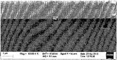
图1是利用本发明制备的过渡族金属ZrNx氮化物薄膜的断面形貌图。Fig. 1 is a cross-sectional morphology diagram of a transition metal ZrNx nitride thin film prepared by the present invention.
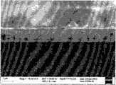
图2是利用本发明制备的过渡族金属HfNx氮化物薄膜的断面形貌图。Fig. 2 is a cross-sectional morphology diagram of a transition metal HfNx nitride thin film prepared by the present invention.
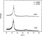
图3是利用本发明制备的过渡族金属(Zr,Hf)Nx氮化物薄膜的X-射线衍射图谱。Fig. 3 is an X-ray diffraction pattern of transition metal (Zr, Hf) Nx nitride film prepared by the present invention.
图4是利用本发明,在ZnS基片上制备(Zr,Hf)Nx氮化物保护膜前后ZnS基片样品的红外透过率随波长变化的曲线。Fig. 4 is a curve of the infrared transmittance of the ZnS substrate sample before and after preparing the (Zr, Hf)Nx nitride protective film on the ZnS substrate as a function of wavelength by using the present invention.
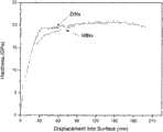
图5是利用本发明,在ZnS基片上制备(Zr,Hf)Nx氮化物保护膜前后ZnS基片样品的纳米硬度-位移曲线。Fig. 5 is the nanohardness-displacement curve of the ZnS substrate sample before and after preparing (Zr, Hf)Nx nitride protective film on the ZnS substrate by using the present invention.
具体实施方式Detailed ways
实施例1Example 1
1.选用物理气相沉积法的溅射法,制备所需的(Zr,Hf)Nx氮化物薄膜。1. Select the sputtering method of the physical vapor deposition method to prepare the required (Zr, Hf)Nx nitride thin film.
2.反应室抽真空至6×10^-3Pa以下,在抽真空的过程中打开基片加热器,设定温度为300℃,通入氩气,流量为8.0sccm,反应室压力为0.50~0.54Pa,打开射频电源,调节基片偏压为-300V,进行预溅射,时间为20分钟,在此过程中靶材和靶材由挡板隔开。2. Vacuumize the reaction chamber to below 6×10^-3Pa, turn on the substrate heater during the vacuuming process, set the temperature at 300°C, feed argon, the flow rate is 8.0sccm, and the reaction chamber pressure is 0.50~ 0.54Pa, turn on the RF power supply, adjust the substrate bias to -300V, and perform pre-sputtering for 20 minutes. During this process, the target and the target are separated by a baffle.
3.预溅射完后,关闭基片电源,调节氩气流量至2.5sccm,打开氮气流量阀,调节氮气流量使N2/Ar流量比值在0.72,调节靶电源设定输入功率为100~300W,移开挡板,开始沉积,沉积压力为0.34~0.41Pa,沉积时间为60分钟。3. After pre-sputtering, turn off the substrate power supply, adjust the argon gas flow rate to 2.5 sccm, open the nitrogen gas flow valve, adjust the nitrogen gas flow rate so that the N2/Ar flow ratio is 0.72, and adjust the target power supply to set the input power to 100-300W. Remove the baffle to start deposition, the deposition pressure is 0.34-0.41Pa, and the deposition time is 60 minutes.
4.沉积结束后,关闭电源和气体流量计,使基片逐渐降温。4. After the deposition is over, turn off the power and the gas flow meter to gradually cool down the substrate.
5.对于上述(Zr,Hf)Nx氮化物薄膜材料的性能测试结果5. Performance test results for the above (Zr, Hf)Nx nitride thin film materials
(1)(Zr,Hf)Nx氮化物薄膜的形貌和组织分析(1) Morphology and structure analysis of (Zr, Hf)Nx nitride film
所获得的(Zr,Hf)Nx氮化物薄膜的断面形貌如图1、2所示,图3为薄膜的X-射线衍射图谱。The cross-sectional morphology of the obtained (Zr, Hf)Nx nitride film is shown in Figures 1 and 2, and Figure 3 is the X-ray diffraction pattern of the film.
(2)红外透过率测试(2) Infrared transmittance test
图4是ZnS基片镀膜前后的红外光谱透射率随波长变化的曲线,从图中可以看到,在8~12μm波段,ZnS+HfNx薄膜的透过率在70%以上,ZnS+ZrNx薄膜的透过率也保持在70%左右。Figure 4 is the curve of the infrared spectral transmittance before and after ZnS substrate coating with wavelength. It can be seen from the figure that in the 8-12 μm band, the transmittance of the ZnS+HfNx film is above 70%, and the transmittance of the ZnS+ZrNx film is more than 70%. The transmittance is also maintained at around 70%.
(3)硬度测试(3) Hardness test
图5为本发明过渡金属Zr、Hf的氮化物薄膜的纳米硬度-位移曲线,从曲线我们可以看到,薄膜的硬度值约为20GPa,远高于ZnS、ZnSe红外光学窗口的硬度。Figure 5 is the nanohardness-displacement curve of the transition metal Zr, Hf nitride thin film of the present invention, we can see from the curve, the hardness value of the thin film is about 20GPa, much higher than the hardness of ZnS, ZnSe infrared optical window.
(4)热冲击测试(4) Thermal shock test
管式恒温炉加热镀膜后的ZnS基片,在200℃保温30min,然后取出迅速放入室温的水中,反复15次。经过此项测试,过渡金属Zr、Hf的氮化物保护膜没有剥落或从基片上剥离,说明膜基之间的具有良好的结合力。Heat the coated ZnS substrate in a tubular constant temperature furnace, keep it at 200°C for 30 minutes, then take it out and put it into room temperature water quickly,
实施例2Example 2
1.选用等离子体辅助的化学气相沉积法,制备所需的(Zr,Hf)Nx氮化物薄膜。1. Select the plasma-assisted chemical vapor deposition method to prepare the required (Zr, Hf)Nx nitride thin film.
2.将反应室抽真空至6×10^-3Pa以下,在抽真空的过程中打开基片加热器,设定其温度为500℃,通入Ar刻蚀5分钟,Ar流量为10sccm,反应室压力5000±100Pa。2. Vacuumize the reaction chamber to below 6×10^-3Pa, turn on the substrate heater during the vacuuming process, set its temperature to 500°C, pass in Ar to etch for 5 minutes, the Ar flow rate is 10sccm, and the reaction Chamber pressure 5000±100Pa.
3.刻蚀完后关闭Ar流量计,再次抽真空至6×10^-3Pa以下,通入氨气和四氯化Zr或四氯化Hf,流量各为25sccm和5sccm,调节反应室压力为5000Pa,打开射频电源,调节功率为500W,开始(Zr,Hf)氮化物薄膜的化学气相沉积,在沉积过程中,气体的流量保持恒定,反应室压力保持在5000±100Pa之间,沉积时间为60分钟。3. After etching, close the Ar flowmeter, evacuate to below 6×10^-3Pa again, feed ammonia gas and Zr tetrachloride or Hf tetrachloride, the flow rates are 25 sccm and 5 sccm respectively, and adjust the pressure of the reaction chamber to 5000Pa, turn on the RF power supply, adjust the power to 500W, and start the chemical vapor deposition of (Zr, Hf) nitride film. During the deposition process, the gas flow rate is kept constant, the reaction chamber pressure is kept between 5000±100Pa, and the deposition time is 60 minutes.
4.沉积完毕后,阶梯式降温:450℃-350℃-250℃-150℃-20℃。4. After the deposition is completed, the temperature is lowered stepwise: 450°C-350°C-250°C-150°C-20°C.
5.对上述(Zr,Hf)Nx氮化物薄膜材料的性能测试结果与图1-5相仿。5. The performance test results of the above (Zr, Hf)Nx nitride thin film materials are similar to those shown in Figures 1-5.
Claims (5)
Translated fromChinesePriority Applications (1)
| Application Number | Priority Date | Filing Date | Title |
|---|---|---|---|
| CN2010101955098ACN101887134A (en) | 2010-05-31 | 2010-05-31 | A kind of infrared window protective film material, its application and preparation method |
Applications Claiming Priority (1)
| Application Number | Priority Date | Filing Date | Title |
|---|---|---|---|
| CN2010101955098ACN101887134A (en) | 2010-05-31 | 2010-05-31 | A kind of infrared window protective film material, its application and preparation method |
Publications (1)
| Publication Number | Publication Date |
|---|---|
| CN101887134Atrue CN101887134A (en) | 2010-11-17 |
Family
ID=43073125
Family Applications (1)
| Application Number | Title | Priority Date | Filing Date |
|---|---|---|---|
| CN2010101955098APendingCN101887134A (en) | 2010-05-31 | 2010-05-31 | A kind of infrared window protective film material, its application and preparation method |
Country Status (1)
| Country | Link |
|---|---|
| CN (1) | CN101887134A (en) |
Cited By (2)
| Publication number | Priority date | Publication date | Assignee | Title |
|---|---|---|---|---|
| CN102477579A (en)* | 2010-11-30 | 2012-05-30 | 天津津航技术物理研究所 | Method for obtaining znse/zns optical element |
| CN103443658A (en)* | 2012-03-09 | 2013-12-11 | 住友电气工业株式会社 | Optical component and manufacturing method therefor |
Citations (7)
| Publication number | Priority date | Publication date | Assignee | Title |
|---|---|---|---|---|
| CN1097890A (en)* | 1993-02-03 | 1995-01-25 | 迪吉普雷斯公司 | Be used to make master of the mould that voltage supply system particular optical disk uses and preparation method thereof |
| CN1100812A (en)* | 1993-04-28 | 1995-03-29 | 美国Boc氧气集团有限公司 | Durable low-emissivity solar control thin film coating |
| CN1115467A (en)* | 1994-02-21 | 1996-01-24 | 迪吉普雷斯公司 | Preformatted substrate, preformatted substrate comprising information to be duplicated, their processest of manufacture and process of manufacture of a naster disk and/or of an optical disk |
| CN101072734A (en)* | 2004-11-08 | 2007-11-14 | 格拉沃贝尔公司 | Glazing |
| CN101231352A (en)* | 2007-06-11 | 2008-07-30 | 北京有色金属研究总院 | HfON/BP antireflecting protective film for infrared optical window and manufacture method thereof |
| JP2009267192A (en)* | 2008-04-28 | 2009-11-12 | Mitsubishi Electric Corp | Manufacturing method for semiconductor device and semiconductor manufacturing device |
| CN101636362A (en)* | 2007-01-15 | 2010-01-27 | 法国圣戈班玻璃厂 | Glass substrate coated with layers having an improved mechanical strength |
- 2010
- 2010-05-31CNCN2010101955098Apatent/CN101887134A/enactivePending
Patent Citations (7)
| Publication number | Priority date | Publication date | Assignee | Title |
|---|---|---|---|---|
| CN1097890A (en)* | 1993-02-03 | 1995-01-25 | 迪吉普雷斯公司 | Be used to make master of the mould that voltage supply system particular optical disk uses and preparation method thereof |
| CN1100812A (en)* | 1993-04-28 | 1995-03-29 | 美国Boc氧气集团有限公司 | Durable low-emissivity solar control thin film coating |
| CN1115467A (en)* | 1994-02-21 | 1996-01-24 | 迪吉普雷斯公司 | Preformatted substrate, preformatted substrate comprising information to be duplicated, their processest of manufacture and process of manufacture of a naster disk and/or of an optical disk |
| CN101072734A (en)* | 2004-11-08 | 2007-11-14 | 格拉沃贝尔公司 | Glazing |
| CN101636362A (en)* | 2007-01-15 | 2010-01-27 | 法国圣戈班玻璃厂 | Glass substrate coated with layers having an improved mechanical strength |
| CN101231352A (en)* | 2007-06-11 | 2008-07-30 | 北京有色金属研究总院 | HfON/BP antireflecting protective film for infrared optical window and manufacture method thereof |
| JP2009267192A (en)* | 2008-04-28 | 2009-11-12 | Mitsubishi Electric Corp | Manufacturing method for semiconductor device and semiconductor manufacturing device |
Cited By (4)
| Publication number | Priority date | Publication date | Assignee | Title |
|---|---|---|---|---|
| CN102477579A (en)* | 2010-11-30 | 2012-05-30 | 天津津航技术物理研究所 | Method for obtaining znse/zns optical element |
| CN102477579B (en)* | 2010-11-30 | 2015-01-07 | 天津津航技术物理研究所 | Method for obtaining znse/zns optical element |
| CN103443658A (en)* | 2012-03-09 | 2013-12-11 | 住友电气工业株式会社 | Optical component and manufacturing method therefor |
| CN103443658B (en)* | 2012-03-09 | 2016-05-11 | 住友电气工业株式会社 | Optics and manufacture method thereof |
Similar Documents
| Publication | Publication Date | Title |
|---|---|---|
| CN105296926B (en) | A kind of anti-reflection composite membrane optical window of hard and preparation method thereof | |
| CN104805405B (en) | A kind of aluminum nitride piezoelectric thin film and preparation method thereof | |
| Rubin et al. | Optical and mechanical properties of dc sputtered carbon films | |
| CN104862659B (en) | A kind of medium frequency magnetron reaction sputtering method of aluminium nitride film | |
| CN102965666B (en) | A kind of flexible substrate nano-diamond film and preparation method thereof | |
| TW202111154A (en) | Reinforced nano film of outer cover of electronic equipment and preparation method and application of reinforced nano film | |
| CN108505016A (en) | A kind of deposition method of cvd diamond thick film | |
| CN101024213A (en) | Method for manufacturing wafer carrier protective layer | |
| CN101887134A (en) | A kind of infrared window protective film material, its application and preparation method | |
| CN107546109B (en) | A method for removing silicon carbide on the surface of a diamond window prepared on a silicon substrate using hydrogen plasma | |
| CN111621756B (en) | Method for preparing crystalline transparent alumina film by room temperature sputtering | |
| CN108149210B (en) | A kind of preparation method of long-wave infrared antireflection protective film | |
| CN1065926C (en) | Infrared anti-reflection filter window of diamond and its preparing method | |
| CN105327900A (en) | Method for recovering first mirror reflectivity through magnetic enhanced radio frequency plasma | |
| CN110863188A (en) | Graphite-like hydrogen-containing carbon film, preparation method and optical film | |
| Liao et al. | Characterization of RuO2 thin films deposited on Si by metal-organic chemical vapor deposition | |
| CN108220897A (en) | The method of magnetron sputtering low temperature preparation vanadium dioxide film | |
| CN114959638A (en) | Preparation method of germanium carbide film | |
| CN113529166B (en) | Method for growing large-area diamond single crystal | |
| CN101736313A (en) | Method for preparing diamond-like film on germanium substrate | |
| CN113322522B (en) | Preparation method of large-single-domain large-area single-layer tungsten disulfide film by epitaxy | |
| Vorli et al. | C: N and C: N: O films: preparation and properties | |
| CN106435503A (en) | Silicon oxide film with large positive temperature coefficient and deposition method thereof | |
| Ianno et al. | Plasma-enhanced chemical vapor deposition of molybdenum | |
| CN106835016A (en) | A kind of aluminum nitride piezoelectric film material of Er doping |
Legal Events
| Date | Code | Title | Description |
|---|---|---|---|
| C06 | Publication | ||
| PB01 | Publication | ||
| C10 | Entry into substantive examination | ||
| SE01 | Entry into force of request for substantive examination | ||
| C02 | Deemed withdrawal of patent application after publication (patent law 2001) | ||
| WD01 | Invention patent application deemed withdrawn after publication | Application publication date:20101117 |