CN101882595A - Method and device for removing barrier layer - Google Patents
Method and device for removing barrier layerDownload PDFInfo
- Publication number
- CN101882595A CN101882595ACN2009100508357ACN200910050835ACN101882595ACN 101882595 ACN101882595 ACN 101882595ACN 2009100508357 ACN2009100508357 ACN 2009100508357ACN 200910050835 ACN200910050835 ACN 200910050835ACN 101882595 ACN101882595 ACN 101882595A
- Authority
- CN
- China
- Prior art keywords
- tantalum
- titanium
- oxide film
- barrier layer
- layer
- Prior art date
- Legal status (The legal status is an assumption and is not a legal conclusion. Google has not performed a legal analysis and makes no representation as to the accuracy of the status listed.)
- Granted
Links
Images


Landscapes
- Internal Circuitry In Semiconductor Integrated Circuit Devices (AREA)
- Weting (AREA)
Abstract
Description
Translated fromChinese技术领域technical field
本发明是关于半导体加工方法和装置的。确切地说,是关于无应力铜抛光和阻挡层的选择性去除的。更确切地说,本发明涉及的工艺可以用于集成器件制造中选择性地抛光铜和钽/氮化钽阻挡层的无应力去除。This invention relates to semiconductor processing methods and apparatus. Specifically, it is about stress-free copper polishing and selective removal of barrier layers. More specifically, the present invention relates to processes that can be used to selectively polish copper and stress-free removal of tantalum/tantalum nitride barrier layers in integrated device fabrication.
背景技术Background technique
半导体器件是在半导体硅片上经过一系列不同的加工步骤形成晶体管和互连线而成的。为了晶体管终端能和硅片连在一起,需要在硅片的介质材料上做出导电的(例如金属)槽、孔及其他类似的东西作为器件的一部分。槽和孔可以在晶体管之间、内部电路以及外部电路传递电信号和能量。Semiconductor devices are formed by forming transistors and interconnection lines on semiconductor silicon wafers through a series of different processing steps. In order for the transistor terminals to be connected to the silicon chip, conductive (eg metal) slots, holes and the like need to be made in the dielectric material of the silicon chip as part of the device. Slots and holes can transfer electrical signals and energy between transistors, internal circuits, and external circuits.
在形成互连元素时,半导体硅片可能需要掩膜、刻蚀和沉积等工艺来形成晶体管和连接晶体管终端所需要的回路。特别是多层掩膜、离子注入、退火、等离子刻蚀和物理及化学气相沉积等工艺可以用于浅槽和晶体管的阱、门还有多晶硅线和互连新结构。When forming interconnect elements, semiconductor silicon wafers may require processes such as masking, etching, and deposition to form transistors and the circuits required to connect transistor terminals. In particular, processes such as multilayer masking, ion implantation, annealing, plasma etching, and physical and chemical vapor deposition can be used for shallow trenches and wells for transistors, gates, and new structures for polysilicon lines and interconnections.
去除沉积在半导体硅片上电介质材料非凹陷区域的金属薄膜,传统的方法包括化学机械抛光(CMP)。化学机械抛光在半导体工业中应用广泛,可以抛光和平坦化在介质材料的非凹陷区域上形成的槽和孔内的金属层,从而形成互连线。在CMP中被加工的硅片放在平坦的抛光垫上。被加工的硅片的介质基层内包含一层或多层互连元素层或者其他功能层,然后用压力把硅片压在抛光垫上。在硅片表面由于所施加的压力进行抛光时抛光垫和硅片进行着相互运动。在抛光垫上加一种常被称之为磨料的液体使抛光更容易进行。磨料的典型成分包含研磨剂,它可以有选择的进行化学反应,从而把想要抛光的部分去除,比如,它可以只把金属层抛光而对电介质层没有影响。To remove the metal film deposited on the non-recessed area of the dielectric material on the semiconductor silicon wafer, the traditional method includes chemical mechanical polishing (CMP). Chemical mechanical polishing is widely used in the semiconductor industry to polish and planarize the metal layer in the grooves and holes formed on the non-recessed area of the dielectric material, thereby forming the interconnection line. The silicon wafer being processed in CMP rests on a flat polishing pad. The dielectric base layer of the processed silicon wafer contains one or more layers of interconnect elements or other functional layers, and then the silicon wafer is pressed against the polishing pad by pressure. The polishing pad and the silicon wafer are in mutual motion when the surface of the silicon wafer is polished due to the applied pressure. Adding a liquid, often called an abrasive, to the polishing pad makes polishing easier. Typical components of abrasives include abrasives, which selectively chemically react to remove the part to be polished, for example, it can only polish the metal layer without affecting the dielectric layer.
由于其中的强机械作用力,CMP方法会对半导体结构带来一些有害的影响。例如当互连线的尺寸减小到0.13微米及以下时导电材料,由于铜和低k电介质材料的机械性能有很大差别。低k电介质材料的杨氏模量的值与铜和阻挡层材料的杨氏模量的值相差10倍以上。那么CMP中相对较强的机械作用力可能会对低k电介质材料造成永久性的损坏。Due to the strong mechanical forces involved, the CMP method can have some detrimental effects on the semiconductor structure. Conductive materials such as copper and low-k dielectric materials have very different mechanical properties as the size of interconnect lines decreases to 0.13 microns and below. The value of the Young's modulus of the low-k dielectric material is more than 10 times different from that of the copper and barrier layer materials. Then the relatively strong mechanical force in CMP may cause permanent damage to the low-k dielectric material.
另一种去除半导体介质材料非凹陷区域上沉积的金属膜的方法是电化学抛光。电化学铜抛光系统可以很均匀地实现铜去除,并且对阻挡层钽/氮化钽材料有很高的选择比。这是一种无机械应力的抛光方法,但是阻挡层由于其表面形成了氧化物钝化层而不能用电抛光的方法去除。Another method for removing the metal film deposited on the non-recessed areas of the semiconductor dielectric material is electrochemical polishing. The electrochemical copper polishing system can achieve very uniform copper removal and has a high selectivity for barrier layer tantalum/tantalum nitride materials. This is a polishing method without mechanical stress, but the barrier layer cannot be removed by electropolishing due to the formation of an oxide passivation layer on its surface.
去除钽和氮化钽的一个方法是用氢氟酸湿法刻蚀,但是当阻挡层被去除以后氢氟酸会损坏电介质层。One method of removing tantalum and tantalum nitride is wet etching with hydrofluoric acid, but hydrofluoric acid can damage the dielectric layer after the barrier layer is removed.
另外,Sood等,《基于NaOH和KOH溶液的钽溅射层的湿法去除》,2007年,J Mater Sci揭示:Mater Electron期刊,第18卷,535-539页,讲述了用KOH/H2O2或NaOH/H2O2溶液去除钽的方法.类似KOH或者NaOH的强碱溶液可以加速钽的溶解。然而NaOH/H2O2和KOH/H2O2都一定程度上会刻蚀、损坏槽内的铜。In addition, Sood et al., "Wet Removal of Tantalum Sputtered Layers Based on NaOH and KOH Solutions", 2007, J Mater Sci Revealed: Mater Electron Journal, Volume 18, Pages 535-539, described the use of KOH/H2 O2 or NaOH/H2 O2 solution to remove tantalum. A strong alkaline solution like KOH or NaOH can accelerate the dissolution of tantalum. However, both NaOH/H2 O2 and KOH/H2 O2 will etch and damage the copper in the groove to a certain extent.
IBM的专利揭示:一种新的加工技术即在铜的CMP工艺后用二氟化氙气相刻蚀法来去除阻挡层材料,例如:钽、氮化钽、钛和氮化钛。IBM's patent discloses: a new processing technology that uses xenon difluoride gas phase etching to remove barrier layer materials such as tantalum, tantalum nitride, titanium and titanium nitride after the CMP process of copper.
发明内容Contents of the invention
本发明是关于半导体芯片加工方法和装置的。半导体芯片基底包括衬底、电介质层、位于电介质层上的阻挡层和阻挡层上的铜金属层。更具体地说,本发明是关于工艺:铜的无应力电化学抛光工艺、在铜抛光过程中形成的钽或钛的氧化物的去除和阻挡层钽/氮化钽或钛/氮化钛用二氟化氙气相刻蚀方法去除工艺.The present invention relates to a semiconductor chip processing method and device. The semiconductor chip base includes a substrate, a dielectric layer, a barrier layer on the dielectric layer, and a copper metal layer on the barrier layer. More specifically, the present invention relates to processes: stress-free electrochemical polishing of copper, removal of tantalum or titanium oxides formed during copper polishing, and barrier layers for tantalum/tantalum nitride or titanium/titanium nitride Removal process of xenon difluoride vapor phase etching method.
首先,用无应力抛光方法把电镀铜中多余的铜膜去除。本发明用无应力电化学抛光的方法代替了传统的铜的化学机械抛光(CMP)方法作为半导体制造后段中基本的“金属抛光工艺”。这是一个电化学工艺过程:半导体硅片上的铜作为阳极,电解液喷嘴作为阴极。当两极之间施加一定的电压,铜就可以被与之接触的电解液抛光。当覆在上面的铜被去除后,暴露出来的钽或钛表面会形成一层化学稳定性很高的氧化物钝化膜。First, the excess copper film in the electroplated copper is removed by stress-free polishing. The present invention replaces the traditional copper chemical mechanical polishing (CMP) method with a stress-free electrochemical polishing method as the basic "metal polishing process" in the back stage of semiconductor manufacturing. It's an electrochemical process: copper on a semiconducting silicon wafer acts as the anode, and an electrolyte nozzle acts as the cathode. When a certain voltage is applied between the two poles, the copper can be polished by the electrolyte in contact with it. When the overlying copper is removed, the exposed tantalum or titanium surface forms a highly chemically stable oxide passivation film.
钽或钛的氧化物具有很高的化学稳定性。在铜的无应力抛光过程中它作为阻挡层材料的保护层,但是它也使后续工艺中阻挡层的去除更加困难。二氟化氙气体可以有效的刻蚀钽/氮化钽和钛/氮化钛,但是对氧化钽或氧化钛的刻蚀速率很慢。为了能更有效地去除阻挡层,避免氧化钽或氧化钛引起的阻挡效应,本发明在二氟化氙气体去除钽/氮化钽或钛/氮化钛之前,用一种刻蚀剂先把阻挡层表面的氧化钽或氧化钛去掉。有多种刻蚀剂可以把氧化钽或氧化钛去掉,比如氢氟酸、缓冲氢氟酸、氢氧化钠溶液、氢氧化钾溶液、草酸和柠檬酸等。除了上面的几个刻蚀剂的例子以外,CF4/O2等离子和氩气溅射轰击也可以用来去除阻挡层表面的氧化钽或氧化钛。Oxides of tantalum or titanium are highly chemically stable. It serves as a protective layer for the barrier material during stress-free polishing of copper, but it also makes removal of the barrier more difficult in subsequent processes. Xenon difluoride gas can effectively etch tantalum/tantalum nitride and titanium/titanium nitride, but the etching rate of tantalum oxide or titanium oxide is very slow. In order to remove the barrier layer more effectively and avoid the barrier effect caused by tantalum oxide or titanium oxide, the present invention uses an etchant to remove tantalum/tantalum nitride or titanium/titanium nitride before xenon difluoride gas. The tantalum oxide or titanium oxide on the surface of the barrier layer is removed. There are various etchants that can remove tantalum oxide or titanium oxide, such as hydrofluoric acid, buffered hydrofluoric acid, sodium hydroxide solution, potassium hydroxide solution, oxalic acid, and citric acid. In addition to the above few etchant examples, CF4 /O2 plasma and argon sputtering bombardment can also be used to remove tantalum oxide or titanium oxide on the surface of the barrier layer.
最后用二氟化氙气相刻蚀的方法把阻挡层钽/氮化钽或钛/氮化钛去除。本发明用二氟化氙气相刻蚀来代替传统的钽/氮化钽或钛/氮化钛化学机械抛光作为基本的阻挡层去除工艺。以上工艺都是没有机械作用力的,因此对低k材料和器件结构不会有机械上的损坏。Finally, the barrier layer tantalum/tantalum nitride or titanium/titanium nitride is removed by xenon difluoride gas phase etching. The present invention uses xenon difluoride gas phase etching to replace traditional tantalum/tantalum nitride or titanium/titanium nitride chemical mechanical polishing as the basic barrier layer removal process. The above processes have no mechanical force, so there will be no mechanical damage to low-k materials and device structures.
关于本发明的更多优点可以通过下面的详细说明和附带的示意图得到体现。Further advantages of the present invention can be realized through the following detailed description and accompanying schematic diagrams.
附图说明Description of drawings
图1是在铜无应力电化学抛光之前,半导体硅片上互连结构的横切面示意图。Figure 1 is a schematic cross-sectional view of an interconnect structure on a semiconductor silicon wafer prior to stress-free electrochemical polishing of copper.
图2是在铜无应力电化学抛光之后,半导体硅片上互连结构的横切面示意图。在抛光过程中阻挡层的表面形成了一层氧化钽或氧化钛薄膜。2 is a schematic cross-sectional view of an interconnect structure on a semiconductor silicon wafer after stress-free electrochemical polishing of copper. During the polishing process, a layer of tantalum oxide or titanium oxide film is formed on the surface of the barrier layer.
图3是半导体硅片上氧化钽或氧化钛薄膜被去除以后互连结构的横切面示意图。Fig. 3 is a schematic cross-sectional view of the interconnection structure after the tantalum oxide or titanium oxide film on the semiconductor silicon wafer is removed.
图4是半导体硅片阻挡层钽/氮化钽或钛/氮化钛用二氟化氙气相刻蚀掉之后的横切面示意图。Fig. 4 is a schematic cross-sectional view of the semiconductor wafer barrier layer of tantalum/tantalum nitride or titanium/titanium nitride after gas phase etching away with xenon difluoride.
图5是本发明中的一个工艺流程图示例。Fig. 5 is an example of a process flow diagram in the present invention.
图6是本发明中装置的框架的示例图。Fig. 6 is an example diagram of the frame of the device in the present invention.
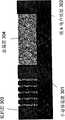
图7是样品在无应力抛光之后扫描电子显微镜(SEM)的俯视图片,该样品用二氟化氙直接刻蚀而没有把阻挡层表面的氧化钽提前去除,图7中的箭头所指为针孔的位置。Fig. 7 is a top view picture of a scanning electron microscope (SEM) of the sample after stress-free polishing. The sample is directly etched with xenon difluoride without removing the tantalum oxide on the surface of the barrier layer in advance. The arrow in Fig. 7 is the needle hole location.
图8是样品在无应力抛光之后扫描电子显微镜(SEM)的俯视图片。该样品用较强的氧化钽刻蚀剂处理过,图8中的箭头所指为阻挡层(钽/氮化钽)的侧壁损伤。Figure 8 is a top view picture of the sample by scanning electron microscope (SEM) after stress-free polishing. The sample was treated with a stronger tantalum oxide etchant, and the arrows in Figure 8 indicate sidewall damage to the barrier layer (tantalum/tantalum nitride).
图9是样品在无应力抛光之后扫描电子显微镜(SEM)的俯视图片,该样品是先把氧化钽去除然后用二氟化氙气体把阻挡层去除。Figure 9 is a top-down scanning electron microscope (SEM) image of a sample after stress-free polishing where the tantalum oxide was first removed and then the barrier layer was removed with xenon difluoride gas.
具体实施方式Detailed ways
本发明是关于半导体器件加工方法和装置的。更确切地说,本发明是关于去除或者刻蚀阻挡层例如钽/氮化钽的,该阻挡层适合于低k电介质材料。这样有利于低k材料在半导体器件中的各种应用。The present invention relates to a semiconductor device processing method and device. More specifically, the present invention relates to removing or etching barrier layers, such as tantalum/tantalum nitride, suitable for low-k dielectric materials. This facilitates various applications of low-k materials in semiconductor devices.
图1到图4所示为半导体加工中一些新工艺的结合:用无应力抛光的方法去除铜,用刻蚀剂去除铜抛光过程中阻挡层表面形成的钽的氧化物,用具有选择性的二氟化氙气体刻蚀法去除阻挡层钽/氮化钽。其中无论电化学抛铜,还是氧化钽的去除,还是二氟化氙刻蚀阻挡层都是没有机械作用力的过程。因此这组工艺使半导体结构的机械损伤最小化、使氧化钽的覆盖效应最小化、半导体结构的化学改性最小化,同时使低k介质材料的损失最小化。Figures 1 to 4 show the combination of some new processes in semiconductor processing: using stress-free polishing to remove copper, using etchant to remove tantalum oxide formed on the surface of the barrier layer during copper polishing, and using selective The barrier layer tantalum/tantalum nitride is removed by xenon difluoride gas etching. Among them, no matter the electrochemical copper throwing, the removal of tantalum oxide, or the etching barrier layer of xenon difluoride are all processes without mechanical force. This set of processes thus minimizes mechanical damage to the semiconductor structure, minimizes blanketing effects of tantalum oxide, minimizes chemical modification of the semiconductor structure, and minimizes loss of low-k dielectric material.
图1所示是铜的大马士革结构的示意图。该半导体结构包含了电介质层,通常是在硅片基底或者前面的已加工的半导体器件结构101上形成的低k电介质层102。根据具体实例,低k电介质的介电常数一般大于1.2,小于4.2。该结构还进一步包含有在低k电介质层102上面的阻挡层103,通常是钽/氮化钽或者其他材料。该结构包含被电介质层102分割开的槽和孔的图案。在阻挡层103上的金属或者铜膜104结构是通过填充介质层凹陷区域而成的。但是填充的凹陷区域的同时,非凹陷区域的介质层也会被覆盖。采用以下的方法,这些阻挡层103和介质层102结构上所镀铜或者金属层104的形貌可以很平坦。专利PCT/US03/11417描述了一种方法,在电镀的时候采用假结构。或者采用美国专利60/738250中介绍的方法,用接触垫式喷嘴也可以实现铜或者金属层表面的平坦化。Figure 1 is a schematic diagram of the damascene structure of copper. The semiconductor structure includes a dielectric layer, typically a low-k dielectric layer 102 formed on a silicon substrate or a previously processed semiconductor device structure 101 . According to a specific example, the dielectric constant of the low-k dielectric is generally greater than 1.2 and less than 4.2. The structure further includes a barrier layer 103, typically tantalum/tantalum nitride or other material, on top of the low-k dielectric layer 102 . The structure comprises a pattern of trenches and holes separated by a dielectric layer 102 . The metal or copper film 104 structure on the barrier layer 103 is formed by filling the recessed area of the dielectric layer. But while filling the recessed area, the dielectric layer in the non-recessed area will also be covered. By adopting the following method, the topography of the copper plated or metal layer 104 on the structures of the barrier layer 103 and the dielectric layer 102 can be very flat. Patent PCT/US03/11417 describes a method using dummy structures when electroplating. Alternatively, using the method described in US Patent No. 60/738250, the surface planarization of copper or metal layers can also be achieved by using a contact pad nozzle.
对金属层204进行无应力抛光(图5中的步骤502),图2所示的是硅片经过电抛光之后的结构的横切面图。金属或者铜层204被抛光到了非凹陷区域的表面。因此凹陷区域里填充的金属、槽还有孔等相互之间就分开了。该过程是一种电化学工艺:硅片上的铜作为阳极,电解液喷嘴是阴极。当两极之间加上一定的正电压之后铜就会被电解液溶解。该过程是一个具有选择性的无应力的铜去除过程。阻挡层钽/氮化钽203表面形成了一层氧化物薄膜205而被钝化。该钝化膜在铜的抛光过程中可以起到保护阻挡层的作用,不过阻挡层203上形成的氧化钽薄膜205使得后续的阻挡层去除变得更加困难。Perform stress-free polishing on the metal layer 204 (
在阻挡层的表面形成的氧化钽薄膜205由两部分组成:一部分是由于钽在空气中自然氧化造成的。当钽位于空气中时根据化合价的不同可以形成多种化合物,包括TaO,Ta2O,TaO2,Ta2O5和Ta2O7。但是当有水存在的情况下只有Ta2O5是最稳定的。The tantalum oxide film 205 formed on the surface of the barrier layer consists of two parts: one part is caused by natural oxidation of tantalum in air. When tantalum is in the air, various compounds can be formed according to the valence, including TaO, Ta2 O, TaO2 , Ta2 O5 and Ta2 O7 . But onlyTa2O5 is the most stable in the presenceof water.
另外一部分,也是更重要的一部分是由铜的无应力抛光过程中阳极氧化造成的。在铜的抛光过程中钽被暴露以后,其表面的电极反应可以描述如下:Another part, and a more important part, is caused by anodic oxidation during stress-free polishing of copper. After tantalum is exposed during copper polishing, the electrode reaction on its surface can be described as follows:
2Ta+5H2O=Ta2O5+10H++10e-2Ta+5H2 O=Ta2 O5 +10H+ +10e-
由于电解液中有水的存在,铜抛光完成以后钽表面的氧化物主要是五价氧化钽即五氧化二钽。五氧化二钽具有很高的化学稳定性,在铜抛光的过程中它作为阻挡层的保护层。但它却使后续的阻挡层去除更加困难。二氟化氙气体可以用适当的速率刻蚀掉钽和氮化钽203,但是几乎刻蚀不了氧化钽205,在某些条件下甚至一点都刻蚀不掉。因此它可以阻止钽和氮化钽被去除。很长时间的二氟化氙刻蚀可以去除部分钽和氮化钽,但是只会引起针孔效应。如图7所示,铜无应力抛光以后,在没有经过氧化钽薄膜205去除的情况下,用二氟化氙气体长时间刻蚀钽/氮化钽后的扫描电子显微镜的照片。可以看出在一定的时间以后除了针孔周围的钽/氮化钽部分被去除,其余的阻挡层203根本没有被刻蚀。为了更有效的去除阻挡层必须首先去除钽的氧化层205。Due to the presence of water in the electrolyte, the oxide on the surface of tantalum after copper polishing is mainly pentavalent tantalum oxide, namely tantalum pentoxide. Tantalum pentoxide has high chemical stability, and it acts as a protective layer for the barrier layer during copper polishing. But it makes subsequent barrier removal more difficult. The xenon difluoride gas can etch away tantalum and tantalum nitride 203 at a moderate rate, but it can hardly etch tantalum oxide 205, even under certain conditions. So it prevents tantalum and tantalum nitride from being removed. Long xenon difluoride etch can partially remove tantalum and tantalum nitride, but only cause pinhole effect. As shown in FIG. 7 , after the stress-free polishing of copper, without removing the tantalum oxide film 205 , it is a scanning electron microscope photo of long-time etching of tantalum/tantalum nitride with xenon difluoride gas. It can be seen that after a certain period of time, the rest of the barrier layer 203 is not etched at all except for the tantalum/tantalum nitride portion around the pinhole. In order to remove the barrier layer more effectively, the tantalum oxide layer 205 must be removed first.
因而,在图5中的第二步就是把钽的氧化层去除(步骤504)。下面是为了说明本方法而举的几个实例,本发明并不局限于此。Thus, the second step in FIG. 5 is to remove the tantalum oxide layer (step 504). The following are several examples for illustrating the method, but the present invention is not limited thereto.
去除钽氧化层的第一种方法是用含有F-离子的溶液处理硅片的表面,其中氢氟酸(HF)和氢氟酸的缓冲溶液(BHF)更好。HF/BHF可以跟氧化钽反应,化学反应方程式以五氧化二钽为例,可以表示如下:The first method to remove the tantalum oxide layer is to treat the surface of the silicon wafer with a solution containing F- ions, among which hydrofluoric acid (HF) and a buffered solution of hydrofluoric acid (BHF) are better. HF/BHF can react with tantalum oxide. The chemical reaction equation takes tantalum pentoxide as an example, which can be expressed as follows:
Ta2O5+14F-+10H+=2TaF72-+5H2OTa2 O5 +14F- +10H+ =2TaF72- +5H2 O
HF/BHF的浓度可以从0.1w%到30w%,而浓度介于0.5%--4%之间更好。处理时溶液的温度从0oC到50oC,而室温更好。处理时间的长短跟温度和溶液的浓度都有关系。该溶液可以刻蚀氧化钽薄膜205以及部分钽阻挡层203并且对铜膜204没有任何影响。但是如果刻蚀时间太长或者溶液的浓度太高,阻挡层钽/氮化钽也将被去除。如图8所示,在方块结构周围的钽/氮化钽侧壁已经至少部分地被破坏。从而低k电介质层202也将被该溶液损坏。图9所示是一个铜204抛光之后钽氧化层205正确处理的例子。与图7和8比较可以看出阻挡层钽/氮化钽去除效果非常好。The concentration of HF/BHF can be from 0.1w% to 30w%, and the concentration is better between 0.5%--4%. The temperature of the solution during processing is from 0oC to 50oC, and room temperature is better. The length of the treatment time is related to the temperature and the concentration of the solution. The solution can etch the tantalum oxide film 205 and part of the tantalum barrier layer 203 without any influence on the copper film 204 . But if the etching time is too long or the concentration of the solution is too high, the barrier layer tantalum/tantalum nitride will also be removed. As shown in FIG. 8, the Ta/TaN sidewalls around the block structure have been at least partially destroyed. Thus the low-k dielectric layer 202 will also be damaged by the solution. FIG. 9 is an example of correct processing of tantalum oxide layer 205 after copper 204 polishing. Comparing Figures 7 and 8, it can be seen that the barrier Ta/TaN removal is very good.
含F-离子的溶液不只局限于HF和BH F.溶液中含有F-,pH值小于7并且对铜没有损坏都可以用作钽氧化物薄膜205的刻蚀剂。例如含有硫酸或者盐酸的NH4F溶液。并且在溶液中加入其他的酸可以使氧化钽的去除更加有效,因为有更低的pH值。氧化钽薄膜205的去除效果可以通过调节F-浓度和pH值来控制。The solution containing F- ions is not limited to HF and BHF. The solution containing F- , pH value less than 7 and no damage to copper can be used as an etchant for the tantalum oxide film 205 . For example, NH4 F solution containing sulfuric acid or hydrochloric acid. And adding other acids to the solution can make the removal of tantalum oxide more effective because of the lower pH. The removal effect of the tantalum oxide film 205 can be controlled by adjusting the F- concentration and pH value.
去除氧化钽薄膜的第二种方法是使用强碱溶液作为刻蚀剂。氧化钽薄膜205可以溶解于强碱溶液,因为在碱溶液中可以形成钽的矿物酸。在本发明所述的情况下是钽酸(H2Ta2O6)。五氧化二钽在高pH值的溶液或者高温度的溶液中可以加快溶解。例如氢氧化钾溶液在室温下饱和溶液的pH值大于10,浓度从0.1%到50%,而10%~40%更好。温度从0℃到90℃,而40℃到80℃更好。强碱溶液对氧化钽薄膜205和铜薄膜204的刻蚀速率选择比也很高。The second method to remove the tantalum oxide film is to use a strong alkaline solution as an etchant. The tantalum oxide film 205 can be dissolved in a strong alkaline solution, because a mineral acid of tantalum can be formed in the alkaline solution. In the case of the present invention it is tantalic acid (H2 Ta2 O6 ). Tantalum pentoxide can accelerate dissolution in solutions with high pH value or high temperature. For example, the pH value of a saturated solution of potassium hydroxide solution at room temperature is greater than 10, and the concentration is from 0.1% to 50%, and 10% to 40% is better. The temperature is from 0°C to 90°C, more preferably 40°C to 80°C. The selective ratio of the etching rate of the strong alkali solution to the tantalum oxide film 205 and the copper film 204 is also very high.
第三种去除氧化钽薄膜205的方法是用一种刻蚀气体混合物,包括大约300sccm到400sccm的CF4和大约200sccm到600sccm的氧气,温度从大约100℃到150℃,压强从1torr到1.5torr。刻蚀气体跟钽的氧化层接触是以等离子的形式进行的。等离子可以通过反应离子刻蚀装置(RIE)或者电子回旋共振(ECR)等离子发生器,RIE和ECR都是广泛商业应用的,而平行板RIE更好。用刻蚀气体去除钽的氧化层是各向同性的,具有很好的均匀性。The third method for removing the tantalum oxide film 205 is to use an etching gas mixture comprising about 300 sccm to 400 sccm of CF4 and about 200 sccm to 600 sccm of oxygen at a temperature of about 100° C. to 150° C. and a pressure of 1 torr to 1.5 torr . The contact between the etching gas and the oxide layer of tantalum is carried out in the form of plasma. Plasma can be generated by reactive ion etching (RIE) or electron cyclotron resonance (ECR) plasma generators. Both RIE and ECR are widely used commercially, and parallel plate RIE is better. The removal of the tantalum oxide layer by etching gas is isotropic and has good uniformity.
去除氧化钽薄膜205的第四种方法是用气体溅射轰击法。比如氩气溅射轰击就像薄膜沉积的反过程,靠高速的粒子把表面的氧化钽逐步剥离。溅射用的稀有气体是从下面气体中的一种或几种:氦气、氖气、氩气、氪气和氙气,其中氩气更好。溅射用的设备是目前商业上广泛应用的。The fourth method for removing the tantalum oxide film 205 is gas sputtering bombardment. For example, argon sputtering bombardment is like the reverse process of thin film deposition, and the tantalum oxide on the surface is gradually peeled off by high-speed particles. The rare gas used for sputtering is one or more of the following gases: helium, neon, argon, krypton and xenon, among which argon is better. Equipment for sputtering is currently commercially available.
去除氧化钽薄膜205的第五种方法是用草酸或者柠檬酸做刻蚀剂。草酸或者柠檬酸溶液至少可以去除部分氧化钽薄膜层205,使阻挡层203的去除更有效。酸的浓度从0.1%到10%,而5%~8%更好。刻蚀的温度从0℃到80℃,而20℃~60℃更好。A fifth method for removing the tantalum oxide film 205 is to use oxalic acid or citric acid as an etchant. The oxalic acid or citric acid solution can remove at least part of the tantalum oxide thin film layer 205 to make the removal of the barrier layer 203 more effective. The acid concentration is from 0.1% to 10%, and 5% to 8% is better. The etching temperature is from 0°C to 80°C, more preferably 20°C to 60°C.
所有以上的示例方法均可以用来去除钽的氧化物层但是HF/BHF更好。前面也曾提到,这里列举的例子是为了说明步骤504去除钽氧化物薄膜205甚至部分阻挡层钽203的工艺。如图3所示,在钽的氧化物薄膜205去除之后,阻挡层303钽/氮化钽和铜层304就露出来了。All the above example methods can be used to remove the tantalum oxide layer but HF/BHF is better. As mentioned above, the example given here is to illustrate the process of removing the tantalum oxide film 205 and even part of the barrier layer tantalum 203 in
在表面的氧化钽薄膜205被去除以后,二氟化氙气体把在硅片表面剩余的阻挡层303钽/氮化钽去除(图5中的步骤506)。二氟化氙气体在一定的温度和压强下可以和阻挡层303钽/氮化钽自发地发生化学反应。二氟化氙气体对铜404和电介质材料402都有很好的选择性,比如SiO2,SiLK,和基于Si-C-O-H的低k材料,k值从1.2到4.2,而1.3~2.4更好。在整个工艺过程中不会对阻挡层403或介质层402产生任何直接的机械应力,因而对铜404和低k电介质材料402不会产生物理损坏。衬底的温度从0℃到300℃,而25℃~200℃更好。二氟化氙气体的压强从0.1Torr到100Torr,而0.5Torr~20Torr更好。After the tantalum oxide film 205 on the surface is removed, the xenon difluoride gas removes the remaining barrier layer 303 tantalum/tantalum nitride on the surface of the silicon wafer (
二氟化氙与阻挡层303钽/氮化钽反应的产物是气相的(氙气和氧气)或者在该工艺条件下是可以升华的(氟化钽)。因此在硅片表面上不会有残留物。The products of the reaction of xenon difluoride with barrier layer 303 tantalum/tantalum nitride are in the gas phase (xenon and oxygen) or sublimable under the process conditions (tantalum fluoride). Therefore there will be no residues on the wafer surface.
如图4所示,当表面上的阻挡层用二氟化氙气相刻蚀法506完全去除干净以后,槽和孔在电学上完全分开了。金属层或铜层404、阻挡层403彻底被电介质材料402隔离开了。As shown in FIG. 4, when the barrier layer on the surface is completely removed by xenon difluoride
图6是本发明中装置的示意框架图。该装置包括:无应力的电化学铜抛光系统(SFP)602,钽的氧化物层去除系统604和二氟化氙气相刻蚀系统606。上述子系统602-606分别对应着图5中的502-506工艺步骤。Fig. 6 is a schematic frame diagram of the device in the present invention. The apparatus includes: a stress-free electrochemical copper polishing system (SFP) 602 , a tantalum oxide
一个典型的例子,电抛光系统包含一个电解液喷嘴,电解液就是通过该喷嘴喷到硅片不同半径的地方。一个电源负极接到喷嘴上,通过喷嘴为电解液供负电压。电源的正极与硅片相连接为硅片提供正电压。因而在电化学抛光过程中喷嘴作为阴极,而硅片作为阳极。当电解液不断地流到硅片上的金属层时,由于两者之间的电势差硅片表面的金属层被抛光。虽然这里提到硅片是直接与电源的正极相连的,但需要注意的是电源的正极和硅片之间可以插入任意数量的连接件。例如,电源可以跟硅片夹相连,而硅片夹再与硅片相连,更确切地说是与硅片上的金属层相连。关于更详细的电化学抛光系统的描述可以参考美国专利号为09/497,894专利标题是《半导体器件互连金属的抛光方法和装置》,发表于2000年2月4日。这里把整个专利作为参考文献。A typical example, an electropolishing system includes an electrolyte nozzle through which electrolyte is sprayed onto the silicon wafer at different radii. A negative electrode of a power supply is connected to the nozzle, and a negative voltage is supplied to the electrolyte through the nozzle. The positive electrode of the power supply is connected with the silicon chip to provide positive voltage for the silicon chip. Therefore, the nozzle acts as the cathode and the silicon wafer acts as the anode during the electrochemical polishing process. When the electrolyte continuously flows to the metal layer on the silicon wafer, the metal layer on the surface of the silicon wafer is polished due to the potential difference between the two. Although it is mentioned here that the silicon chip is directly connected to the positive terminal of the power supply, it should be noted that any number of connections can be inserted between the positive terminal of the power supply and the silicon chip. For example, the power supply can be connected to a wafer clip, which in turn is connected to the silicon die, more specifically, to a metal layer on the silicon die. For a more detailed description of the electrochemical polishing system, refer to US Patent No. 09/497,894 titled "Method and Apparatus for Polishing Interconnect Metals of Semiconductor Devices", published on February 4, 2000. The entire patent is incorporated herein by reference.
一个典型例子,阻挡层氧化物薄膜去除系统包括一个可以旋转的硅片夹来固定硅片,其中旋转是指驱动该硅片夹围绕着一个轴转动;一个把刻蚀剂喷到硅片表面的喷嘴;一个腔体和刻蚀剂输送系统。在铜的无应力抛光之后,硅片就被放到上述的硅片夹内。当硅片夹开始转动后,刻蚀剂均匀地喷洒到硅片的表面。经过一定时间以后阻挡层的氧化物薄膜就被去除干净。As a typical example, the barrier oxide film removal system includes a rotatable silicon wafer holder to fix the silicon wafer, wherein rotation refers to driving the silicon wafer holder to rotate around an axis; a device that sprays etchant onto the surface of the silicon wafer nozzle; a chamber and etchant delivery system. After stress-free polishing of the copper, the silicon wafer is placed in the wafer holder described above. When the wafer clamp starts to rotate, the etchant is evenly sprayed onto the surface of the wafer. After a certain period of time, the oxide film of the barrier layer is removed.
一个典型的例子,本发明的二氟化氙刻蚀系统与现在商业上应用的硅的微系统加工(MEMS)系统较为相似,包括:至少一个真空泵,一个刻蚀腔,一个扩散腔,个固体二氟化氙源腔、温度控制系统和自动化控制系统。每个腔之间都用气动节流阀控制。并且在扩散腔和刻蚀腔内还有真空计或压力表。该系统既可以工作在脉冲模式下也可以在恒流模式下工作。在恒流模式下,刻蚀腔和扩散腔内的压力保持恒定以便控制刻蚀速率。在脉冲模式下,两个腔首先用高纯氮气净化,然后抽成真空。把二氟化氙瓶子的开关打开,气体就可以填充到扩散腔。然后把二氟化氙瓶子开关关闭,把扩散腔和刻蚀腔之间的节流阀打开,当刻蚀腔内的压强达到一定数值后就可以把节流阀关闭。当硅片跟二氟化氙气体接触一定时间后,比如3-30秒,把刻蚀腔抽成真空,反应的副产物被排出腔体。到此便完成了脉冲模式下的一个“循环”。并且可以根据需要重复若干次该循环,直到硅片表面的阻挡层的钽/氮化钽被去除干净露出电介质层。本发明中的二氟化氙刻蚀系统也是没有应力的。A typical example, the xenon difluoride etching system of the present invention is comparatively similar to the silicon microsystem processing (MEMS) system that commercially applies now, comprises: at least one vacuum pump, an etching chamber, a diffusion chamber, a solid Xenon difluoride source chamber, temperature control system and automatic control system. Each chamber is controlled by a pneumatic throttle valve. And there are vacuum gauges or pressure gauges in the diffusion chamber and the etching chamber. The system can work both in pulse mode and in constant current mode. In constant flow mode, the pressure in the etch chamber and the diffusion chamber is kept constant to control the etch rate. In pulsed mode, both chambers are first purged with high-purity nitrogen and then evacuated. Turn on the switch of the xenon difluoride bottle, and the gas can be filled into the diffusion chamber. Then turn off the xenon difluoride bottle switch, open the throttle valve between the diffusion chamber and the etching chamber, and close the throttle valve when the pressure in the etching chamber reaches a certain value. After the silicon wafer is in contact with the xenon difluoride gas for a certain period of time, such as 3-30 seconds, the etching chamber is evacuated, and the by-products of the reaction are discharged from the chamber. At this point, a "cycle" in the pulse mode is completed. And this cycle can be repeated several times as required, until the tantalum/tantalum nitride of the barrier layer on the surface of the silicon wafer is completely removed to expose the dielectric layer. The xenon difluoride etch system of the present invention is also stress free.
尽管本发明的描述中提到了大量的具体的实物、方法和应用的例子,但是本发明并不局限于此。Although numerous specific examples of objects, methods and applications have been mentioned in the description of the invention, the invention is not limited thereto.
Claims (23)
Translated fromChinesePriority Applications (2)
| Application Number | Priority Date | Filing Date | Title |
|---|---|---|---|
| CN200910050835.7ACN101882595B (en) | 2009-05-08 | 2009-05-08 | Method and device for removing barrier layer |
| CN201410257649.1ACN103985670B (en) | 2009-05-08 | 2009-05-08 | The minimizing technology and device on barrier layer |
Applications Claiming Priority (1)
| Application Number | Priority Date | Filing Date | Title |
|---|---|---|---|
| CN200910050835.7ACN101882595B (en) | 2009-05-08 | 2009-05-08 | Method and device for removing barrier layer |
Related Child Applications (1)
| Application Number | Title | Priority Date | Filing Date |
|---|---|---|---|
| CN201410257649.1ADivisionCN103985670B (en) | 2009-05-08 | 2009-05-08 | The minimizing technology and device on barrier layer |
Publications (2)
| Publication Number | Publication Date |
|---|---|
| CN101882595Atrue CN101882595A (en) | 2010-11-10 |
| CN101882595B CN101882595B (en) | 2014-07-09 |
Family
ID=43054562
Family Applications (1)
| Application Number | Title | Priority Date | Filing Date |
|---|---|---|---|
| CN200910050835.7AExpired - Fee RelatedCN101882595B (en) | 2009-05-08 | 2009-05-08 | Method and device for removing barrier layer |
Country Status (1)
| Country | Link |
|---|---|
| CN (1) | CN101882595B (en) |
Cited By (23)
| Publication number | Priority date | Publication date | Assignee | Title |
|---|---|---|---|---|
| CN103367138A (en)* | 2012-03-30 | 2013-10-23 | 盛美半导体设备(上海)有限公司 | A technique for vapor etching a barrier layer with xenon difluoride |
| CN103515294A (en)* | 2012-06-26 | 2014-01-15 | 盛美半导体设备(上海)有限公司 | Method for manufacturing tungsten plug |
| CN103692293A (en)* | 2012-09-27 | 2014-04-02 | 盛美半导体设备(上海)有限公司 | Stress-free polishing device and polishing method |
| CN103839876A (en)* | 2012-11-27 | 2014-06-04 | 盛美半导体设备(上海)有限公司 | Method and device for manufacturing semiconductor device |
| CN104143525A (en)* | 2013-05-09 | 2014-11-12 | 盛美半导体设备(上海)有限公司 | Metal planarization method on back side of TSV |
| CN104143526A (en)* | 2013-05-09 | 2014-11-12 | 盛美半导体设备(上海)有限公司 | Fabrication method of TSV structure |
| CN104347481A (en)* | 2013-07-31 | 2015-02-11 | 盛美半导体设备(上海)有限公司 | Metal coating processing method |
| CN104637863A (en)* | 2013-11-14 | 2015-05-20 | 盛美半导体设备(上海)有限公司 | Tungsten plug formation method |
| CN104637862A (en)* | 2013-11-14 | 2015-05-20 | 盛美半导体设备(上海)有限公司 | Method for forming semiconductor structures |
| CN104952787A (en)* | 2014-03-26 | 2015-09-30 | 盛美半导体设备(上海)有限公司 | Automatic correcting method for radial thickness |
| CN106328580A (en)* | 2015-06-30 | 2017-01-11 | 盛美半导体设备(上海)有限公司 | Vapor phase etching method of copper interconnection structure |
| CN107210261A (en)* | 2015-02-15 | 2017-09-26 | 盛美半导体设备(上海)有限公司 | Remove the method that barrier layer minimizes side walls collapse |
| CN107331768A (en)* | 2016-04-29 | 2017-11-07 | 上海磁宇信息科技有限公司 | A kind of lithographic method of MTJ bilayer conductive hard mask |
| CN107346760A (en)* | 2016-05-05 | 2017-11-14 | 盛美半导体设备(上海)有限公司 | A kind of processing method of interconnection structure |
| CN107437581A (en)* | 2016-05-25 | 2017-12-05 | 上海磁宇信息科技有限公司 | A kind of preparation method using tantalum oxide as the MTJ of hard mask |
| TWI608541B (en)* | 2011-11-17 | 2017-12-11 | 盛美半導體設備(上海)有限公司 | Method for forming air gap interconnection structure |
| CN108417528A (en)* | 2018-02-05 | 2018-08-17 | 武汉新芯集成电路制造有限公司 | A Method for Improving Residue on Aluminum Pads |
| CN108493205A (en)* | 2018-04-10 | 2018-09-04 | 武汉新芯集成电路制造有限公司 | A method of it eliminating aluminium pad and reacts defect with developer solution |
| CN108886016A (en)* | 2016-04-07 | 2018-11-23 | 盛美半导体设备(上海)有限公司 | Planarization process and device of TSV structure |
| CN109463005A (en)* | 2016-06-03 | 2019-03-12 | 恩特格里斯公司 | Vapor Phase Etching of Hafnium Dioxide and Zirconium Dioxide |
| CN110504302A (en)* | 2019-08-29 | 2019-11-26 | 上海华力集成电路制造有限公司 | A high-K metal gate structure and its manufacturing method |
| TWI714583B (en)* | 2016-05-16 | 2021-01-01 | 聯華電子股份有限公司 | Semiconductor device and method of forming the same |
| CN114752938A (en)* | 2022-04-07 | 2022-07-15 | 中国科学院赣江创新研究院 | Completely removed Nb3Method for stabilizing layer and blocking layer of Sn superconducting line |
Families Citing this family (1)
| Publication number | Priority date | Publication date | Assignee | Title |
|---|---|---|---|---|
| CN107346731B (en)* | 2016-05-05 | 2021-03-16 | 盛美半导体设备(上海)股份有限公司 | Method for reducing thickness of copper film |
Citations (8)
| Publication number | Priority date | Publication date | Assignee | Title |
|---|---|---|---|---|
| US5254202A (en)* | 1992-04-07 | 1993-10-19 | International Business Machines Corporation | Fabrication of laser ablation masks by wet etching |
| TW512455B (en)* | 2000-06-16 | 2002-12-01 | Infineon Technologies Corp | Clean method for recessed conductive barriers |
| CN1523647A (en)* | 1998-07-09 | 2004-08-25 | ACM�о���˾ | Apparatus for electropolishing metal interconnections on semiconductor devices |
| CN1543668A (en)* | 2001-08-17 | 2004-11-03 | Acm研究公司 | Semiconductor structure formation using a combination of planarization and electropolishing |
| TW200506098A (en)* | 2003-03-26 | 2005-02-16 | Mitsubishi Gas Chemical Co | Etching agent composition for thin films having high permittivity and process for etching |
| CN1788330A (en)* | 2003-03-28 | 2006-06-14 | 反射公司 | Barrier layers for microelectromechanical systems |
| US7422700B1 (en)* | 2005-06-28 | 2008-09-09 | Novellus Systems, Inc. | Compositions and methods of electrochemical removal of material from a barrier layer of a wafer |
| US20090001587A1 (en)* | 2005-02-24 | 2009-01-01 | International Business Machines Corporation | Ta-TaN SELECTIVE REMOVAL PROCESS FOR INTEGRATED DEVICE FABRICATION |
- 2009
- 2009-05-08CNCN200910050835.7Apatent/CN101882595B/ennot_activeExpired - Fee Related
Patent Citations (8)
| Publication number | Priority date | Publication date | Assignee | Title |
|---|---|---|---|---|
| US5254202A (en)* | 1992-04-07 | 1993-10-19 | International Business Machines Corporation | Fabrication of laser ablation masks by wet etching |
| CN1523647A (en)* | 1998-07-09 | 2004-08-25 | ACM�о���˾ | Apparatus for electropolishing metal interconnections on semiconductor devices |
| TW512455B (en)* | 2000-06-16 | 2002-12-01 | Infineon Technologies Corp | Clean method for recessed conductive barriers |
| CN1543668A (en)* | 2001-08-17 | 2004-11-03 | Acm研究公司 | Semiconductor structure formation using a combination of planarization and electropolishing |
| TW200506098A (en)* | 2003-03-26 | 2005-02-16 | Mitsubishi Gas Chemical Co | Etching agent composition for thin films having high permittivity and process for etching |
| CN1788330A (en)* | 2003-03-28 | 2006-06-14 | 反射公司 | Barrier layers for microelectromechanical systems |
| US20090001587A1 (en)* | 2005-02-24 | 2009-01-01 | International Business Machines Corporation | Ta-TaN SELECTIVE REMOVAL PROCESS FOR INTEGRATED DEVICE FABRICATION |
| US7422700B1 (en)* | 2005-06-28 | 2008-09-09 | Novellus Systems, Inc. | Compositions and methods of electrochemical removal of material from a barrier layer of a wafer |
Cited By (35)
| Publication number | Priority date | Publication date | Assignee | Title |
|---|---|---|---|---|
| TWI608541B (en)* | 2011-11-17 | 2017-12-11 | 盛美半導體設備(上海)有限公司 | Method for forming air gap interconnection structure |
| CN103367138A (en)* | 2012-03-30 | 2013-10-23 | 盛美半导体设备(上海)有限公司 | A technique for vapor etching a barrier layer with xenon difluoride |
| CN103367138B (en)* | 2012-03-30 | 2018-04-13 | 盛美半导体设备(上海)有限公司 | The technique of xenon difluoride gas phase etching barrier layer |
| CN103515294A (en)* | 2012-06-26 | 2014-01-15 | 盛美半导体设备(上海)有限公司 | Method for manufacturing tungsten plug |
| CN103692293A (en)* | 2012-09-27 | 2014-04-02 | 盛美半导体设备(上海)有限公司 | Stress-free polishing device and polishing method |
| CN103692293B (en)* | 2012-09-27 | 2018-01-16 | 盛美半导体设备(上海)有限公司 | non-stress polishing device and polishing method |
| CN103839876A (en)* | 2012-11-27 | 2014-06-04 | 盛美半导体设备(上海)有限公司 | Method and device for manufacturing semiconductor device |
| CN103839876B (en)* | 2012-11-27 | 2018-05-18 | 盛美半导体设备(上海)有限公司 | The manufacturing method and device of semiconductor devices |
| CN104143526B (en)* | 2013-05-09 | 2019-05-17 | 盛美半导体设备(上海)有限公司 | Through-silicon-via construction manufacturing method |
| CN104143526A (en)* | 2013-05-09 | 2014-11-12 | 盛美半导体设备(上海)有限公司 | Fabrication method of TSV structure |
| CN104143525A (en)* | 2013-05-09 | 2014-11-12 | 盛美半导体设备(上海)有限公司 | Metal planarization method on back side of TSV |
| CN104143525B (en)* | 2013-05-09 | 2018-12-18 | 盛美半导体设备(上海)有限公司 | Through-silicon-via back metal flattening method |
| CN104347481B (en)* | 2013-07-31 | 2019-10-25 | 盛美半导体设备(上海)有限公司 | Coat of metal processing method |
| CN104347481A (en)* | 2013-07-31 | 2015-02-11 | 盛美半导体设备(上海)有限公司 | Metal coating processing method |
| CN104637862A (en)* | 2013-11-14 | 2015-05-20 | 盛美半导体设备(上海)有限公司 | Method for forming semiconductor structures |
| CN104637863A (en)* | 2013-11-14 | 2015-05-20 | 盛美半导体设备(上海)有限公司 | Tungsten plug formation method |
| CN104952787A (en)* | 2014-03-26 | 2015-09-30 | 盛美半导体设备(上海)有限公司 | Automatic correcting method for radial thickness |
| CN107210261A (en)* | 2015-02-15 | 2017-09-26 | 盛美半导体设备(上海)有限公司 | Remove the method that barrier layer minimizes side walls collapse |
| CN107210261B (en)* | 2015-02-15 | 2021-03-12 | 盛美半导体设备(上海)股份有限公司 | Method for removing barrier layer to minimize sidewall recess |
| CN106328580A (en)* | 2015-06-30 | 2017-01-11 | 盛美半导体设备(上海)有限公司 | Vapor phase etching method of copper interconnection structure |
| CN106328580B (en)* | 2015-06-30 | 2021-05-14 | 盛美半导体设备(上海)股份有限公司 | Vapor etching method of copper interconnection structure |
| CN108886016A (en)* | 2016-04-07 | 2018-11-23 | 盛美半导体设备(上海)有限公司 | Planarization process and device of TSV structure |
| CN108886016B (en)* | 2016-04-07 | 2023-03-10 | 盛美半导体设备(上海)股份有限公司 | Planarization process and device of TSV structure |
| CN107331768B (en)* | 2016-04-29 | 2020-07-07 | 上海磁宇信息科技有限公司 | Etching method of magnetic tunnel junction double-layer conductive hard mask |
| CN107331768A (en)* | 2016-04-29 | 2017-11-07 | 上海磁宇信息科技有限公司 | A kind of lithographic method of MTJ bilayer conductive hard mask |
| CN107346760A (en)* | 2016-05-05 | 2017-11-14 | 盛美半导体设备(上海)有限公司 | A kind of processing method of interconnection structure |
| TWI714583B (en)* | 2016-05-16 | 2021-01-01 | 聯華電子股份有限公司 | Semiconductor device and method of forming the same |
| CN107437581A (en)* | 2016-05-25 | 2017-12-05 | 上海磁宇信息科技有限公司 | A kind of preparation method using tantalum oxide as the MTJ of hard mask |
| CN107437581B (en)* | 2016-05-25 | 2020-10-09 | 上海磁宇信息科技有限公司 | Preparation method of magnetic tunnel junction with tantalum oxide as hard mask |
| CN109463005A (en)* | 2016-06-03 | 2019-03-12 | 恩特格里斯公司 | Vapor Phase Etching of Hafnium Dioxide and Zirconium Dioxide |
| CN109463005B (en)* | 2016-06-03 | 2023-12-15 | 恩特格里斯公司 | Vapor phase etching of hafnium dioxide and zirconium dioxide |
| CN108417528A (en)* | 2018-02-05 | 2018-08-17 | 武汉新芯集成电路制造有限公司 | A Method for Improving Residue on Aluminum Pads |
| CN108493205A (en)* | 2018-04-10 | 2018-09-04 | 武汉新芯集成电路制造有限公司 | A method of it eliminating aluminium pad and reacts defect with developer solution |
| CN110504302A (en)* | 2019-08-29 | 2019-11-26 | 上海华力集成电路制造有限公司 | A high-K metal gate structure and its manufacturing method |
| CN114752938A (en)* | 2022-04-07 | 2022-07-15 | 中国科学院赣江创新研究院 | Completely removed Nb3Method for stabilizing layer and blocking layer of Sn superconducting line |
Also Published As
| Publication number | Publication date |
|---|---|
| CN101882595B (en) | 2014-07-09 |
Similar Documents
| Publication | Publication Date | Title |
|---|---|---|
| CN101882595B (en) | Method and device for removing barrier layer | |
| KR101492467B1 (en) | Barrier layer removal method and apparatus | |
| US9514953B2 (en) | Methods for barrier layer removal | |
| US5849639A (en) | Method for removing etching residues and contaminants | |
| JP2002110647A (en) | Method for manufacturing semiconductor integrated circuit device | |
| WO2005117123A1 (en) | Soi substrate and method for producing same | |
| AU2001241447A1 (en) | Method for low temperature bonding and bonded structure | |
| US12062556B2 (en) | Methods and apparatus for cleaning semiconductor wafers | |
| TW569330B (en) | Forming a semiconductor structure using a combination of planarizing methods and electropolishing | |
| TW201903828A (en) | Oxide film removing method oxide film removing apparatus contact forming method and contact forming system | |
| US20040253809A1 (en) | Forming a semiconductor structure using a combination of planarizing methods and electropolishing | |
| CN113135549A (en) | Method for forming semiconductor device and semiconductor device | |
| TWI501302B (en) | Barrier removal method and device | |
| CN103985670B (en) | The minimizing technology and device on barrier layer | |
| JP4584592B2 (en) | Improved method for etching vias | |
| TWI774645B (en) | Planarization device for TSV structure | |
| US7288487B1 (en) | Metal/oxide etch after polish to prevent bridging between adjacent features of a semiconductor structure | |
| CN113059405A (en) | Processing method and cleaning device for semiconductor structure | |
| US6863769B2 (en) | Configuration and method for making contact with the back surface of a semiconductor substrate | |
| US7517802B2 (en) | Method for reducing foreign material concentrations in etch chambers | |
| CN106298504A (en) | The method of thinning grid oxic horizon and the manufacture method of MOS device | |
| JP2000340544A (en) | Method for manufacturing semiconductor device | |
| US20230108117A1 (en) | Method for Etching of Metal | |
| TW451349B (en) | Planarization process of film layer in semiconductor process | |
| JP3320379B2 (en) | Manufacturing method of bonded substrate |
Legal Events
| Date | Code | Title | Description |
|---|---|---|---|
| C06 | Publication | ||
| PB01 | Publication | ||
| C10 | Entry into substantive examination | ||
| SE01 | Entry into force of request for substantive examination | ||
| C14 | Grant of patent or utility model | ||
| GR01 | Patent grant | ||
| PE01 | Entry into force of the registration of the contract for pledge of patent right | Denomination of invention:Method and device for removing barrier layer Effective date of registration:20151008 Granted publication date:20140709 Pledgee:Bank of China Limited by Share Ltd. Shanghai Development Zone Pudong branch Pledgor:ACM (SHANGHAI) Inc. Registration number:2015310000038 | |
| PLDC | Enforcement, change and cancellation of contracts on pledge of patent right or utility model | ||
| PC01 | Cancellation of the registration of the contract for pledge of patent right | Date of cancellation:20160713 Granted publication date:20140709 Pledgee:Bank of China Limited by Share Ltd. Shanghai Development Zone Pudong branch Pledgor:ACM (SHANGHAI) Inc. Registration number:2015310000038 | |
| PLDC | Enforcement, change and cancellation of contracts on pledge of patent right or utility model | ||
| PE01 | Entry into force of the registration of the contract for pledge of patent right | Denomination of invention:Method and device for removing barrier layer Effective date of registration:20160722 Granted publication date:20140709 Pledgee:Bank of China Limited by Share Ltd. Shanghai Development Zone Pudong branch Pledgor:ACM (SHANGHAI) Inc. Registration number:2016310000031 | |
| PLDC | Enforcement, change and cancellation of contracts on pledge of patent right or utility model | ||
| PC01 | Cancellation of the registration of the contract for pledge of patent right | ||
| PC01 | Cancellation of the registration of the contract for pledge of patent right | Date of cancellation:20191025 Granted publication date:20140709 Pledgee:Bank of China Limited by Share Ltd. Shanghai Development Zone Pudong branch Pledgor:ACM (SHANGHAI) Inc. Registration number:2016310000031 | |
| CP03 | Change of name, title or address | ||
| CP03 | Change of name, title or address | Address after:201203 building 4, No. 1690, Cailun Road, free trade zone, Pudong New Area, Shanghai Patentee after:Shengmei semiconductor equipment (Shanghai) Co.,Ltd. Address before:201203 Shanghai Zhangjiang hi tech park, building 4, No. 1690 Cailun Road Patentee before:ACM (SHANGHAI) Inc. | |
| CF01 | Termination of patent right due to non-payment of annual fee | ||
| CF01 | Termination of patent right due to non-payment of annual fee | Granted publication date:20140709 |