CN101874401A - Single chip image sensor for measuring vitality of object - Google Patents
Single chip image sensor for measuring vitality of objectDownload PDFInfo
- Publication number
- CN101874401A CN101874401ACN200880111898ACN200880111898ACN101874401ACN 101874401 ACN101874401 ACN 101874401ACN 200880111898 ACN200880111898 ACN 200880111898ACN 200880111898 ACN200880111898 ACN 200880111898ACN 101874401 ACN101874401 ACN 101874401A
- Authority
- CN
- China
- Prior art keywords
- light
- infrared
- intensity
- image sensor
- pixel
- Prior art date
- Legal status (The legal status is an assumption and is not a legal conclusion. Google has not performed a legal analysis and makes no representation as to the accuracy of the status listed.)
- Granted
Links
- 238000000034methodMethods0.000claimsdescription18
- 230000035899viabilityEffects0.000abstractdescription3
- 230000003287optical effectEffects0.000description9
- 241000196324EmbryophytaSpecies0.000description5
- 239000000872bufferSubstances0.000description4
- 238000007796conventional methodMethods0.000description3
- 238000001228spectrumMethods0.000description3
- 206010034960PhotophobiaDiseases0.000description2
- 238000010586diagramMethods0.000description2
- 208000013469light sensitivityDiseases0.000description2
- 238000000411transmission spectrumMethods0.000description2
- 244000025254Cannabis sativaSpecies0.000description1
- 230000009286beneficial effectEffects0.000description1
- 239000003086colorantSubstances0.000description1
- 238000005259measurementMethods0.000description1
- 239000004065semiconductorSubstances0.000description1
- 239000000758substrateSubstances0.000description1
- 238000002834transmittanceMethods0.000description1
Images


Classifications
- H—ELECTRICITY
- H04—ELECTRIC COMMUNICATION TECHNIQUE
- H04N—PICTORIAL COMMUNICATION, e.g. TELEVISION
- H04N25/00—Circuitry of solid-state image sensors [SSIS]; Control thereof
- H—ELECTRICITY
- H04—ELECTRIC COMMUNICATION TECHNIQUE
- H04N—PICTORIAL COMMUNICATION, e.g. TELEVISION
- H04N25/00—Circuitry of solid-state image sensors [SSIS]; Control thereof
- H04N25/10—Circuitry of solid-state image sensors [SSIS]; Control thereof for transforming different wavelengths into image signals
- H04N25/11—Arrangement of colour filter arrays [CFA]; Filter mosaics
- H04N25/13—Arrangement of colour filter arrays [CFA]; Filter mosaics characterised by the spectral characteristics of the filter elements
- H04N25/131—Arrangement of colour filter arrays [CFA]; Filter mosaics characterised by the spectral characteristics of the filter elements including elements passing infrared wavelengths
- H—ELECTRICITY
- H04—ELECTRIC COMMUNICATION TECHNIQUE
- H04N—PICTORIAL COMMUNICATION, e.g. TELEVISION
- H04N23/00—Cameras or camera modules comprising electronic image sensors; Control thereof
- H04N23/10—Cameras or camera modules comprising electronic image sensors; Control thereof for generating image signals from different wavelengths
- H04N23/12—Cameras or camera modules comprising electronic image sensors; Control thereof for generating image signals from different wavelengths with one sensor only
- H—ELECTRICITY
- H04—ELECTRIC COMMUNICATION TECHNIQUE
- H04N—PICTORIAL COMMUNICATION, e.g. TELEVISION
- H04N23/00—Cameras or camera modules comprising electronic image sensors; Control thereof
- H04N23/80—Camera processing pipelines; Components thereof
- H04N23/84—Camera processing pipelines; Components thereof for processing colour signals
- H—ELECTRICITY
- H04—ELECTRIC COMMUNICATION TECHNIQUE
- H04N—PICTORIAL COMMUNICATION, e.g. TELEVISION
- H04N25/00—Circuitry of solid-state image sensors [SSIS]; Control thereof
- H04N25/10—Circuitry of solid-state image sensors [SSIS]; Control thereof for transforming different wavelengths into image signals
- H04N25/11—Arrangement of colour filter arrays [CFA]; Filter mosaics
- H04N25/13—Arrangement of colour filter arrays [CFA]; Filter mosaics characterised by the spectral characteristics of the filter elements
- H04N25/135—Arrangement of colour filter arrays [CFA]; Filter mosaics characterised by the spectral characteristics of the filter elements based on four or more different wavelength filter elements
Landscapes
- Engineering & Computer Science (AREA)
- Multimedia (AREA)
- Signal Processing (AREA)
- Physics & Mathematics (AREA)
- Spectroscopy & Molecular Physics (AREA)
- Solid State Image Pick-Up Elements (AREA)
- Image Input (AREA)
- Investigating Or Analysing Materials By Optical Means (AREA)
- Studio Devices (AREA)
- Color Television Image Signal Generators (AREA)
Abstract
Description
Translated fromChinese技术领域technical field
本发明涉及图像传感器,更具体地,涉及用于获取可见光图像和IR(红外)图像的单芯片活力(vitality)测量图像传感器。The present invention relates to image sensors, and more particularly, to single-chip vitality measurement image sensors for acquiring visible light images and IR (infrared) images.
背景技术Background technique
近红外光大量地在植物的叶子、草等上被反射。通过比较图1所示的近红外图像和可见光图像,可测量植物的活力。近红外光的波长在700到900纳米的范围内。根据这些图片测量的植物活力可用作识别植物生长状态的指标(indicator)。此外,所述活力可用作测量待售植物新鲜程度的指标。The near-infrared light is largely reflected on leaves of plants, grass, and the like. Plant vigor can be measured by comparing the near-infrared and visible light images shown in Figure 1. Near-infrared light has a wavelength in the range of 700 to 900 nanometers. The plant vigor measured from these pictures can be used as an indicator for identifying the growth state of the plant. Furthermore, the vigor can be used as an indicator to measure the freshness of the plants for sale.
有一种获取可见光图像和近红外图像的方法,其中使用分束器、可见光图像传感器和红外图像传感器。There is a method of acquiring visible light images and near-infrared images in which a beam splitter, a visible light image sensor, and an infrared image sensor are used.
图2是用于解释使用图像传感器的传统方法的视图。参照图2,包含可见光和红外光的光10入射到透镜21上。通过透镜21的光10由分束器22分离,以被传送到红外截止滤光器23和红外通过滤光器25。红外截止滤光器23从光10中滤掉红外光,并将可见光束传送到第一传感器24。红外通过滤光器25仅使光10中的红外光通过,并将红外光传送到第二传感器26。第一传感器24是输出可见光图像的可见光图像传感器,第二传感器26是输出红外图像的红外图像传感器。FIG. 2 is a view for explaining a conventional method of using an image sensor. Referring to FIG. 2 , light 10 including visible light and infrared light is incident on a
通过第一传感器24和第二传感器26获取的可见光图像和近红外图像由图像信号处理器(ISP)处理。在ISP处理图像之前,可见光图像和近红外图像暂时存储在帧缓存器中。Visible light images and near-infrared images acquired by the
在获取可见光图像和近红外图像的方法中,包括红外截止滤光器23和红外通过滤光器25的光学滤光器不容易操作,而且需要识别几个图像中的相同点的复杂操作。此外,由于需要复杂的帧缓存器和光学器件,因此增加了成本。In the method of acquiring visible light images and near-infrared images, the optical filters including the
发明内容Contents of the invention
技术问题technical problem
本发明提供了一种使用图像传感器测量物体活力的方法。The present invention provides a method for measuring the vitality of an object using an image sensor.
技术方案Technical solutions
根据本发明的一个方面,提供了一种通过使用图像传感器测量物体活力的方法,该方法包括:通过图像传感器接收在物体上反射的、通过透镜的光;从入射到交替排列在图像传感器上的多个红外像素和多个可见光像素上的光,获取红外光强度和色光强度;以及通过比较红外光强度和色光强度,测量物体的活力。According to one aspect of the present invention, there is provided a method of measuring the vitality of an object by using an image sensor, the method comprising: receiving light reflected on the object through the lens through the image sensor; Light on a plurality of infrared pixels and a plurality of visible light pixels to obtain infrared light intensity and color light intensity; and measure the vitality of an object by comparing the infrared light intensity and color light intensity.
根据本发明的另外一个方面,提供了通过使用图像传感器测量物体活力的方法,该方法包括:通过图像传感器接收在物体上反射的、通过透镜的光;从入射到交替排列在图像传感器上的多个白色像素和多个可见光像素上的光,获取红外光强度和色光强度;以及通过比较红外光强度和色光强度,测量物体的活力。According to another aspect of the present invention, there is provided a method for measuring the vitality of an object by using an image sensor, the method comprising: using the image sensor to receive light reflected on the object and passing through the lens; light on a white pixel and multiple visible pixels to obtain infrared light intensity and color light intensity; and measure the vitality of an object by comparing the infrared light intensity and color light intensity.
有益效果Beneficial effect
在根据本发明的图像传感器中,物体的活力是通过使用排列在单个芯片上的可见光像素和红外像素测量的。因此,在图像传感器中不需要复杂的帧缓存器和光学器件,因此有可能降低成本。In the image sensor according to the present invention, the vitality of an object is measured by using visible light pixels and infrared pixels arranged on a single chip. Therefore, complex frame buffers and optics are not required in the image sensor, thus potentially reducing costs.
附图说明Description of drawings
图1是示出了近红外图像和可见光图像的视图;FIG. 1 is a view showing a near-infrared image and a visible light image;
图2是用于解释使用图像传感器的传统方法的视图;FIG. 2 is a view for explaining a conventional method using an image sensor;
图3是用于解释根据本发明的一个实施方式使用图像传感器的方法的视图;FIG. 3 is a view for explaining a method of using an image sensor according to an embodiment of the present invention;
图4是示出了图3中的图像传感器的像素阵列的视图;FIG. 4 is a view showing a pixel array of the image sensor in FIG. 3;
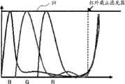
图5是示出了根据第一个实施例,使蓝(B)光、绿(G)光、红(R)光和红外(IR)光通过的滤光器的特性的视图;5 is a view showing characteristics of an optical filter passing blue (B) light, green (G) light, red (R) light, and infrared (IR) light according to the first embodiment;
图6是示出了具有图5的色传输光谱(color transmission spectra)的滤光器的布局图;FIG. 6 is a layout diagram showing an optical filter having the color transmission spectrum of FIG. 5;
图7是示出了根据第二个实施例,使蓝(B)光、绿(G)光、红(R)光和红外(IR)光通过的滤光器的特性的视图;7 is a view showing characteristics of an optical filter passing blue (B) light, green (G) light, red (R) light, and infrared (IR) light according to the second embodiment;
图8是示出了具有图7的色传输光谱的滤光器的布局图;FIG. 8 is a layout diagram showing an optical filter having the color transmission spectrum of FIG. 7;
图9是示出了与图4、图7和图8相关联的图像传感器的横截面视图。FIG. 9 is a cross-sectional view illustrating the image sensor associated with FIGS. 4 , 7 and 8 .
具体实施方式Detailed ways
参考用于描述本发明示例性实施方式的附图以便于充分理解本发明、其优点以及通过实施本发明所达到的目标。The accompanying drawings for describing exemplary embodiments of the present invention are referred to in order to fully understand the present invention, its advantages, and objects achieved by implementing the present invention.
在下文中,将通过参照附图说明本发明的示例性实施方式来详细描述本发明。附图中相同的参考数字表示相同的元件。Hereinafter, the present invention will be described in detail by explaining exemplary embodiments of the invention with reference to the accompanying drawings. Like reference numerals denote like elements in the figures.
图3是用于解释根据本发明的一个实施方式使用图像传感器的方法的视图。FIG. 3 is a view for explaining a method of using an image sensor according to one embodiment of the present invention.
参照图3,包含可见光和红外光的光30入射到透镜31上,以被传送到图像传感器32。Referring to FIG. 3 ,
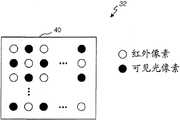
图像传感器32具有图4所示的像素阵列。The
参照图4,可见光像素和红外像素交替排列在芯片40上。Referring to FIG. 4 , visible light pixels and infrared pixels are alternately arranged on the
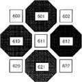
图5是示出了根据第一个实施例,使蓝(B)光、绿(G)光、红(R)光和红外(IR)光通过的滤光器(filter)的特性的视图。具有图5所示的色通光谱(color passing spectra)的滤光器按照图6所示的方式排列在图4所示的像素阵列上。FIG. 5 is a view showing characteristics of filters passing blue (B) light, green (G) light, red (R) light, and infrared (IR) light according to the first embodiment. Filters having the color passing spectrum shown in FIG. 5 are arranged on the pixel array shown in FIG. 4 in the manner shown in FIG. 6 .
参照图4和图6,滤光器601、610、612和621排列在图4所示的可见光像素上,滤光器602、611、620和622排列在红外像素上。例如,滤光器601和621可以是绿光通过(pass)滤光器,滤光器610可以是红光通过滤光器,以及滤光器612可以是蓝光通过滤光器。滤光器611、602、620和622可以是红外通过滤光器。在该实施方式中,红光通过滤光器611、602、620和622可比滤光器601、610、612和621大。或者,滤光器601,610,612和621可配置有不同的颜色。Referring to FIG. 4 and FIG. 6, the
参照图4和图6,描述了根据入射到与滤光器611对应的红外像素(在下文中,称之为点611像素)的红外光来测量活力的方法。点611像素的红光强度、绿光强度和蓝光强度根据相邻的像素计算得到。在估算红光强度、绿光强度和蓝光强度的一个实施例中,点611像素的色光强度(color strength)估算如下:R=(点610像素),G={(点601像素)+(点621像素)}/2,以及B=(点612像素)。可通过比较所估算的、点611像素的色光强度和点611像素的红外光强度,计算活力。为了便于描述,假定当所有波长上的反射率一致时,日光的白斑(white patch)中的红光强度、绿光强度和蓝光强度以及红外光强度都是1。如果该情况下的活力设为1,那么物体的活力定义如下。Referring to FIGS. 4 and 6 , a method of measuring vitality based on infrared light incident to an infrared pixel corresponding to the filter 611 (hereinafter, referred to as a
[等式1][equation 1]
(活力)=2*IR/(R+IR)(Vigor)=2*IR/(R+IR)
例如,具有反射率为R=0.5和IR=1的物体的活力是2/1.5=1.33。For example, the vibrancy of an object with reflectance R=0.5 and IR=1 is 2/1.5=1.33.
这里,基于红外光滤光器和红光滤光器610的特性以及图像传感器32的特性确定红外光灵敏度和红光灵敏度。Here, the infrared light sensitivity and the red light sensitivity are determined based on the characteristics of the infrared light filter and the
在测量可见光像素的活力的方法中,获取可见光像素的红光强度,并且估算可见光像素的红外光强度。然后,通过等式1计算活力。In the method of measuring the viability of a visible light pixel, the red light intensity of the visible light pixel is obtained, and the infrared light intensity of the visible light pixel is estimated. Viability was then calculated by
由此,可由执行等式1操作的ISP计算物体在每个点处的活力。在物体上反射的光通过透镜31传送,以入射到与红外像素相邻的色像素上。在ISP中,处理红外像素的红外光强度和色像素的红光强度,以获得活力图像。Thus, the vitality of the object at each point can be calculated by the ISP performing the operation of
因此,在图像传感器32中,不需要用于存储红外图像和彩色图像的帧缓存器和传统技术所需的光学器件。Therefore, in the
图7是示出了根据第二个实施例,使蓝(B)光、绿(G)、红(R)光和红外(IR)光通过的滤光器的特性的视图。参照图7,蓝光滤光器、绿光滤光器和红光滤光器的特性是:相应的特定光谱通过,远红外区域中的透射率增加。远红外截止滤光器滤掉了远红外光。FIG. 7 is a view showing characteristics of an optical filter passing blue (B) light, green (G), red (R) light, and infrared (IR) light according to the second embodiment. Referring to FIG. 7, the characteristics of the blue filter, the green filter, and the red filter are that the transmittance in the far-infrared region is increased by passing a corresponding specific spectrum. The far-infrared cut filter filters out far-infrared light.
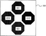
具有图7所示的色通光谱的滤光器按照图8所示的方式排列在图4所示的像素阵列上。此外,能够检测到所有蓝光、绿光、红光和红外光的白色像素排列在图4所示的红外像素的位置上。参照图8,绿光通过滤光器601和621、蓝光通过滤光器612和红光通过滤光器620排列在图4所示的可见光像素上,以及远红外截止滤光器801排列在所有像素上。The filters with the color pass spectrum shown in FIG. 7 are arranged on the pixel array shown in FIG. 4 in the manner shown in FIG. 8 . In addition, white pixels capable of detecting all blue light, green light, red light, and infrared light are arranged at the positions of the infrared pixels shown in FIG. 4 . Referring to Fig. 8, green
图9是示出了与图4、图7和图8相关联的图像传感器的横截面视图。例如,参照图9,蓝光滤光器610和绿光滤光器601排列在形成于半导体衬底90上的可见光像素(蓝色像素和绿色像素)上。远红外截止滤光器排列在滤色器610和601上。因此,通过将白色像素的强度W减去相邻滤色器的红光强度、绿光强度和蓝光强度,得到白色像素的红外光强度。在图像传感器中,不需要仅使红外光通过的红外光滤光器。FIG. 9 is a cross-sectional view illustrating the image sensor associated with FIGS. 4 , 7 and 8 . For example, referring to FIG. 9 , a
尽管本发明是参考其示例性实施方式进行具体的说明和描述,本领域的技术人员将理解在不背离所附权利要求限定的本发明精神和范围的情况下,可进行各种形式和细节上的改变。Although the invention has been particularly illustrated and described with reference to exemplary embodiments thereof, it will be understood by those skilled in the art that changes in form and details may be made without departing from the spirit and scope of the invention as defined in the appended claims. change.
Claims (5)
Translated fromChineseApplications Claiming Priority (3)
| Application Number | Priority Date | Filing Date | Title |
|---|---|---|---|
| KR1020070104957AKR100858034B1 (en) | 2007-10-18 | 2007-10-18 | Single chip vitality image sensor |
| KR10-2007-0104957 | 2007-10-18 | ||
| PCT/KR2008/005862WO2009051363A2 (en) | 2007-10-18 | 2008-10-07 | One chip image sensor for measuring vitality of subject |
Publications (2)
| Publication Number | Publication Date |
|---|---|
| CN101874401Atrue CN101874401A (en) | 2010-10-27 |
| CN101874401B CN101874401B (en) | 2012-12-05 |
Family
ID=40022951
Family Applications (1)
| Application Number | Title | Priority Date | Filing Date |
|---|---|---|---|
| CN2008801118982AActiveCN101874401B (en) | 2007-10-18 | 2008-10-07 | Single-chip image sensor for measuring object vitality |
Country Status (5)
| Country | Link |
|---|---|
| US (1) | US8222603B2 (en) |
| EP (1) | EP2201752A2 (en) |
| KR (1) | KR100858034B1 (en) |
| CN (1) | CN101874401B (en) |
| WO (1) | WO2009051363A2 (en) |
Cited By (3)
| Publication number | Priority date | Publication date | Assignee | Title |
|---|---|---|---|---|
| CN105611136A (en)* | 2016-02-26 | 2016-05-25 | 联想(北京)有限公司 | Image sensor and electronic equipment |
| CN106412389A (en)* | 2015-07-31 | 2017-02-15 | 双光圈国际株式会社 | Sensor assembly with selective infrared filter array |
| CN107018294A (en)* | 2015-09-30 | 2017-08-04 | 三星电子株式会社 | Electronic installation |
Families Citing this family (67)
| Publication number | Priority date | Publication date | Assignee | Title |
|---|---|---|---|---|
| WO2007043036A1 (en) | 2005-10-11 | 2007-04-19 | Prime Sense Ltd. | Method and system for object reconstruction |
| US9330324B2 (en) | 2005-10-11 | 2016-05-03 | Apple Inc. | Error compensation in three-dimensional mapping |
| KR101331543B1 (en) | 2006-03-14 | 2013-11-20 | 프라임센스 엘티디. | Three-dimensional sensing using speckle patterns |
| JP2008306512A (en)* | 2007-06-08 | 2008-12-18 | Nec Corp | Information providing system |
| US8494252B2 (en) | 2007-06-19 | 2013-07-23 | Primesense Ltd. | Depth mapping using optical elements having non-uniform focal characteristics |
| JP2010161636A (en)* | 2009-01-08 | 2010-07-22 | Toyota Central R&D Labs Inc | Filter for imaging apparatus, and shot image processor |
| US8462207B2 (en) | 2009-02-12 | 2013-06-11 | Primesense Ltd. | Depth ranging with Moiré patterns |
| US9986175B2 (en) | 2009-03-02 | 2018-05-29 | Flir Systems, Inc. | Device attachment with infrared imaging sensor |
| US9208542B2 (en) | 2009-03-02 | 2015-12-08 | Flir Systems, Inc. | Pixel-wise noise reduction in thermal images |
| USD765081S1 (en) | 2012-05-25 | 2016-08-30 | Flir Systems, Inc. | Mobile communications device attachment with camera |
| US9451183B2 (en) | 2009-03-02 | 2016-09-20 | Flir Systems, Inc. | Time spaced infrared image enhancement |
| US9517679B2 (en) | 2009-03-02 | 2016-12-13 | Flir Systems, Inc. | Systems and methods for monitoring vehicle occupants |
| US9998697B2 (en) | 2009-03-02 | 2018-06-12 | Flir Systems, Inc. | Systems and methods for monitoring vehicle occupants |
| US9635285B2 (en) | 2009-03-02 | 2017-04-25 | Flir Systems, Inc. | Infrared imaging enhancement with fusion |
| US9473681B2 (en) | 2011-06-10 | 2016-10-18 | Flir Systems, Inc. | Infrared camera system housing with metalized surface |
| US9235876B2 (en) | 2009-03-02 | 2016-01-12 | Flir Systems, Inc. | Row and column noise reduction in thermal images |
| US9756264B2 (en) | 2009-03-02 | 2017-09-05 | Flir Systems, Inc. | Anomalous pixel detection |
| US9843742B2 (en) | 2009-03-02 | 2017-12-12 | Flir Systems, Inc. | Thermal image frame capture using de-aligned sensor array |
| US10757308B2 (en) | 2009-03-02 | 2020-08-25 | Flir Systems, Inc. | Techniques for device attachment with dual band imaging sensor |
| US10244190B2 (en) | 2009-03-02 | 2019-03-26 | Flir Systems, Inc. | Compact multi-spectrum imaging with fusion |
| US9674458B2 (en) | 2009-06-03 | 2017-06-06 | Flir Systems, Inc. | Smart surveillance camera systems and methods |
| US9948872B2 (en) | 2009-03-02 | 2018-04-17 | Flir Systems, Inc. | Monitor and control systems and methods for occupant safety and energy efficiency of structures |
| US8786682B2 (en) | 2009-03-05 | 2014-07-22 | Primesense Ltd. | Reference image techniques for three-dimensional sensing |
| US9843743B2 (en) | 2009-06-03 | 2017-12-12 | Flir Systems, Inc. | Infant monitoring systems and methods using thermal imaging |
| US9292909B2 (en) | 2009-06-03 | 2016-03-22 | Flir Systems, Inc. | Selective image correction for infrared imaging devices |
| US9819880B2 (en) | 2009-06-03 | 2017-11-14 | Flir Systems, Inc. | Systems and methods of suppressing sky regions in images |
| US9756262B2 (en) | 2009-06-03 | 2017-09-05 | Flir Systems, Inc. | Systems and methods for monitoring power systems |
| US10091439B2 (en) | 2009-06-03 | 2018-10-02 | Flir Systems, Inc. | Imager with array of multiple infrared imaging modules |
| US9716843B2 (en) | 2009-06-03 | 2017-07-25 | Flir Systems, Inc. | Measurement device for electrical installations and related methods |
| KR101048768B1 (en) | 2009-06-10 | 2011-07-15 | (주)실리콘화일 | Image sensor for measuring illuminance, proximity and color temperature |
| WO2011013079A1 (en) | 2009-07-30 | 2011-02-03 | Primesense Ltd. | Depth mapping based on pattern matching and stereoscopic information |
| US8830227B2 (en) | 2009-12-06 | 2014-09-09 | Primesense Ltd. | Depth-based gain control |
| US8982182B2 (en) | 2010-03-01 | 2015-03-17 | Apple Inc. | Non-uniform spatial resource allocation for depth mapping |
| KR101703311B1 (en)* | 2010-03-08 | 2017-02-13 | 삼성전자주식회사 | InfraRed Sensor, Touch Panel and 3D Color Image Sensor Containing the Same |
| US9848134B2 (en) | 2010-04-23 | 2017-12-19 | Flir Systems, Inc. | Infrared imager with integrated metal layers |
| US9207708B2 (en) | 2010-04-23 | 2015-12-08 | Flir Systems, Inc. | Abnormal clock rate detection in imaging sensor arrays |
| US9706138B2 (en) | 2010-04-23 | 2017-07-11 | Flir Systems, Inc. | Hybrid infrared sensor array having heterogeneous infrared sensors |
| KR20110140010A (en)* | 2010-06-24 | 2011-12-30 | 삼성전자주식회사 | Image sensor using near infrared signal |
| WO2012020380A1 (en) | 2010-08-11 | 2012-02-16 | Primesense Ltd. | Scanning projectors and image capture modules for 3d mapping |
| US8408821B2 (en)* | 2010-10-12 | 2013-04-02 | Omnivision Technologies, Inc. | Visible and infrared dual mode imaging system |
| EP2643659B1 (en) | 2010-11-19 | 2019-12-25 | Apple Inc. | Depth mapping using time-coded illumination |
| US9167138B2 (en) | 2010-12-06 | 2015-10-20 | Apple Inc. | Pattern projection and imaging using lens arrays |
| US9030528B2 (en) | 2011-04-04 | 2015-05-12 | Apple Inc. | Multi-zone imaging sensor and lens array |
| CN103828343B (en) | 2011-06-10 | 2017-07-11 | 菲力尔系统公司 | Based on capable image procossing and flexible storage system |
| US9961277B2 (en) | 2011-06-10 | 2018-05-01 | Flir Systems, Inc. | Infrared focal plane array heat spreaders |
| US10079982B2 (en) | 2011-06-10 | 2018-09-18 | Flir Systems, Inc. | Determination of an absolute radiometric value using blocked infrared sensors |
| US9900526B2 (en) | 2011-06-10 | 2018-02-20 | Flir Systems, Inc. | Techniques to compensate for calibration drifts in infrared imaging devices |
| US10841508B2 (en) | 2011-06-10 | 2020-11-17 | Flir Systems, Inc. | Electrical cabinet infrared monitor systems and methods |
| US9058653B1 (en) | 2011-06-10 | 2015-06-16 | Flir Systems, Inc. | Alignment of visible light sources based on thermal images |
| US10169666B2 (en) | 2011-06-10 | 2019-01-01 | Flir Systems, Inc. | Image-assisted remote control vehicle systems and methods |
| US10389953B2 (en) | 2011-06-10 | 2019-08-20 | Flir Systems, Inc. | Infrared imaging device having a shutter |
| US9235023B2 (en) | 2011-06-10 | 2016-01-12 | Flir Systems, Inc. | Variable lens sleeve spacer |
| EP2719167B1 (en) | 2011-06-10 | 2018-08-08 | Flir Systems, Inc. | Low power and small form factor infrared imaging |
| US9706137B2 (en) | 2011-06-10 | 2017-07-11 | Flir Systems, Inc. | Electrical cabinet infrared monitor |
| US10051210B2 (en) | 2011-06-10 | 2018-08-14 | Flir Systems, Inc. | Infrared detector array with selectable pixel binning systems and methods |
| CA2838992C (en) | 2011-06-10 | 2018-05-01 | Flir Systems, Inc. | Non-uniformity correction techniques for infrared imaging devices |
| US9143703B2 (en) | 2011-06-10 | 2015-09-22 | Flir Systems, Inc. | Infrared camera calibration techniques |
| US9509924B2 (en) | 2011-06-10 | 2016-11-29 | Flir Systems, Inc. | Wearable apparatus with integrated infrared imaging module |
| CN104160240B (en) | 2012-02-15 | 2017-02-22 | 苹果公司 | Scanning depth engine |
| US9811884B2 (en) | 2012-07-16 | 2017-11-07 | Flir Systems, Inc. | Methods and systems for suppressing atmospheric turbulence in images |
| US20140098063A1 (en)* | 2012-10-10 | 2014-04-10 | Research In Motion Limited | Electronic device with proximity sensing |
| US9973692B2 (en) | 2013-10-03 | 2018-05-15 | Flir Systems, Inc. | Situational awareness by compressed display of panoramic views |
| KR102159991B1 (en) | 2013-12-27 | 2020-09-25 | 삼성전자주식회사 | Lens shading correction method, image signal processing device and image sensor system therewith |
| US11297264B2 (en) | 2014-01-05 | 2022-04-05 | Teledyne Fur, Llc | Device attachment with dual band imaging sensor |
| US10002893B2 (en) | 2014-05-19 | 2018-06-19 | Samsung Electronics Co., Ltd. | Image sensor including hybrid pixel structure |
| KR101575964B1 (en)* | 2014-07-01 | 2015-12-11 | 재단법인 다차원 스마트 아이티 융합시스템 연구단 | Sensor array included in dual aperture camera |
| US9911023B2 (en) | 2015-08-17 | 2018-03-06 | Hand Held Products, Inc. | Indicia reader having a filtered multifunction image sensor |
Family Cites Families (12)
| Publication number | Priority date | Publication date | Assignee | Title |
|---|---|---|---|---|
| US4037048A (en)* | 1973-04-19 | 1977-07-19 | Calspan Corporation | Process for the interpretation of remotely sensed data |
| JP2000059798A (en) | 1998-08-10 | 2000-02-25 | Sony Corp | Near-infrared light/visible light shared image-pickup device |
| US6252218B1 (en) | 1999-02-02 | 2001-06-26 | Agilent Technologies, Inc | Amorphous silicon active pixel sensor with rectangular readout layer in a hexagonal grid layout |
| KR20040059770A (en)* | 2002-12-30 | 2004-07-06 | 주식회사 하이닉스반도체 | CMOS image sensor having Infrared Filter on wafer level |
| US20040174446A1 (en)* | 2003-02-28 | 2004-09-09 | Tinku Acharya | Four-color mosaic pattern for depth and image capture |
| JP4311988B2 (en)* | 2003-06-12 | 2009-08-12 | アキュートロジック株式会社 | Color filter for solid-state image sensor and color image pickup apparatus using the same |
| JP4578797B2 (en)* | 2003-11-10 | 2010-11-10 | パナソニック株式会社 | Imaging device |
| JP2006033483A (en) | 2004-07-16 | 2006-02-02 | Aisin Seiki Co Ltd | Color imaging device |
| CN100480679C (en) | 2004-09-09 | 2009-04-22 | 北京农业信息技术研究中心 | Measurement and measuring device for crop crown layer pigment ratio |
| KR100649016B1 (en)* | 2004-12-30 | 2006-11-27 | 동부일렉트로닉스 주식회사 | CMOS image sensor and its manufacturing method |
| JP4984634B2 (en)* | 2005-07-21 | 2012-07-25 | ソニー株式会社 | Physical information acquisition method and physical information acquisition device |
| JP4730082B2 (en)* | 2005-12-22 | 2011-07-20 | ソニー株式会社 | Image signal processing apparatus, imaging apparatus, image signal processing method, and computer program |
- 2007
- 2007-10-18KRKR1020070104957Apatent/KR100858034B1/enactiveActive
- 2008
- 2008-10-07WOPCT/KR2008/005862patent/WO2009051363A2/enactiveApplication Filing
- 2008-10-07EPEP08838853Apatent/EP2201752A2/ennot_activeWithdrawn
- 2008-10-07CNCN2008801118982Apatent/CN101874401B/enactiveActive
- 2008-10-07USUS12/681,766patent/US8222603B2/enactiveActive
Cited By (6)
| Publication number | Priority date | Publication date | Assignee | Title |
|---|---|---|---|---|
| CN106412389A (en)* | 2015-07-31 | 2017-02-15 | 双光圈国际株式会社 | Sensor assembly with selective infrared filter array |
| CN107018294A (en)* | 2015-09-30 | 2017-08-04 | 三星电子株式会社 | Electronic installation |
| CN107018294B (en)* | 2015-09-30 | 2020-07-14 | 三星电子株式会社 | Electronic device |
| US10812738B2 (en) | 2015-09-30 | 2020-10-20 | Samsung Electronics Co., Ltd. | Electronic device configured to reduce light loss of possible light image and obtain distance information of an object |
| CN105611136A (en)* | 2016-02-26 | 2016-05-25 | 联想(北京)有限公司 | Image sensor and electronic equipment |
| CN105611136B (en)* | 2016-02-26 | 2019-04-23 | 联想(北京)有限公司 | A kind of imaging sensor and electronic equipment |
Also Published As
| Publication number | Publication date |
|---|---|
| WO2009051363A2 (en) | 2009-04-23 |
| CN101874401B (en) | 2012-12-05 |
| EP2201752A2 (en) | 2010-06-30 |
| KR100858034B1 (en) | 2008-09-10 |
| US20100245826A1 (en) | 2010-09-30 |
| US8222603B2 (en) | 2012-07-17 |
| WO2009051363A3 (en) | 2009-07-16 |
Similar Documents
| Publication | Publication Date | Title |
|---|---|---|
| CN101874401B (en) | Single-chip image sensor for measuring object vitality | |
| US9691802B2 (en) | Image-acquisition device | |
| JP6872137B2 (en) | Signal processing equipment, signal processing methods, and programs | |
| JP6322939B2 (en) | Imaging system and color inspection system | |
| US9188841B2 (en) | Imaging device | |
| CN114586066A (en) | Image processing apparatus, image processing method, and image processing program | |
| EP4224129A1 (en) | Image analysis method, image analysis device, program, and recording medium | |
| LV14207B (en) | Technique & Technique for Multi-spectrum & ampacr> R & D & D & R & Dc with Digital & Amacr RGB Sensor | |
| JP6923897B2 (en) | Filters, imaging devices and imaging systems | |
| WO2022163671A1 (en) | Data processing device, method, and program, optical element, imaging optical system, and imaging device | |
| Vunckx et al. | Accurate video-rate multi-spectral imaging using imec snapshot sensors | |
| Fredembach et al. | Illuminant estimation and detection using near-infrared | |
| US11079277B2 (en) | Spectral imaging device and method | |
| WO2013135311A1 (en) | Method and device for imaging of spectral reflectance at several wavelength bands | |
| CN104937386B (en) | Apparatus for predicting, estimating method, integrated circuit and program | |
| US20230082539A1 (en) | Illuminant correction in an imaging system | |
| JP2012189342A (en) | Microspectrometry apparatus | |
| JP2015210124A (en) | Agriculture monitoring camera | |
| US20240070920A1 (en) | Image processing device, image processing method, and image processing program | |
| RU2366907C1 (en) | Method for digital photoelectric colorimetry | |
| KR20170006073A (en) | Apparatus for concentration detection using led spectrophotometer | |
| Bongiorno et al. | Automatic spectrometer/RGB camera spatial calibration | |
| JP2002323376A (en) | Color information measurement method, display color evaluation method, display color adjustment method, apparatus using the same, and projector manufacturing method | |
| US20240015375A1 (en) | Imaging device | |
| JP2011002287A (en) | Method for obtaining color value from spectral data and colorimeter |
Legal Events
| Date | Code | Title | Description |
|---|---|---|---|
| C06 | Publication | ||
| PB01 | Publication | ||
| C10 | Entry into substantive examination | ||
| SE01 | Entry into force of request for substantive examination | ||
| C14 | Grant of patent or utility model | ||
| GR01 | Patent grant | ||
| ASS | Succession or assignment of patent right | Owner name:LI DAOYONG Free format text:FORMER OWNER: SILICONFILE TECHNOLOGIES INC. Effective date:20140822 | |
| C41 | Transfer of patent application or patent right or utility model | ||
| TR01 | Transfer of patent right | Effective date of registration:20140822 Address after:Gyeonggi Do city of South Korea Patentee after:Li Daoyong Address before:Seoul, South Kerean Patentee before:Siliconfile Technologies Inc. | |
| ASS | Succession or assignment of patent right | Owner name:OUPU TUOLAIEN TECHNOLOGY CO., LTD. Free format text:FORMER OWNER: LI DAOYONG Effective date:20150115 | |
| C41 | Transfer of patent application or patent right or utility model | ||
| TR01 | Transfer of patent right | Effective date of registration:20150115 Address after:Gyeonggi Do, South Korea Patentee after:Europe Putuolaien Technology Co. Ltd. Address before:Gyeonggi Do city of South Korea Patentee before:Li Daoyong |