CN101874226A - Liquid crystal display device - Google Patents
Liquid crystal display deviceDownload PDFInfo
- Publication number
- CN101874226A CN101874226ACN200880117647ACN200880117647ACN101874226ACN 101874226 ACN101874226 ACN 101874226ACN 200880117647 ACN200880117647 ACN 200880117647ACN 200880117647 ACN200880117647 ACN 200880117647ACN 101874226 ACN101874226 ACN 101874226A
- Authority
- CN
- China
- Prior art keywords
- liquid crystal
- pixel electrode
- light
- slit
- crystal indicator
- Prior art date
- Legal status (The legal status is an assumption and is not a legal conclusion. Google has not performed a legal analysis and makes no representation as to the accuracy of the status listed.)
- Granted
Links
Images


Classifications
- G—PHYSICS
- G02—OPTICS
- G02F—OPTICAL DEVICES OR ARRANGEMENTS FOR THE CONTROL OF LIGHT BY MODIFICATION OF THE OPTICAL PROPERTIES OF THE MEDIA OF THE ELEMENTS INVOLVED THEREIN; NON-LINEAR OPTICS; FREQUENCY-CHANGING OF LIGHT; OPTICAL LOGIC ELEMENTS; OPTICAL ANALOGUE/DIGITAL CONVERTERS
- G02F1/00—Devices or arrangements for the control of the intensity, colour, phase, polarisation or direction of light arriving from an independent light source, e.g. switching, gating or modulating; Non-linear optics
- G02F1/01—Devices or arrangements for the control of the intensity, colour, phase, polarisation or direction of light arriving from an independent light source, e.g. switching, gating or modulating; Non-linear optics for the control of the intensity, phase, polarisation or colour
- G02F1/13—Devices or arrangements for the control of the intensity, colour, phase, polarisation or direction of light arriving from an independent light source, e.g. switching, gating or modulating; Non-linear optics for the control of the intensity, phase, polarisation or colour based on liquid crystals, e.g. single liquid crystal display cells
- G02F1/133—Constructional arrangements; Operation of liquid crystal cells; Circuit arrangements
- G02F1/1333—Constructional arrangements; Manufacturing methods
- G02F1/1337—Surface-induced orientation of the liquid crystal molecules, e.g. by alignment layers
- G02F1/133707—Structures for producing distorted electric fields, e.g. bumps, protrusions, recesses, slits in pixel electrodes
- G—PHYSICS
- G02—OPTICS
- G02F—OPTICAL DEVICES OR ARRANGEMENTS FOR THE CONTROL OF LIGHT BY MODIFICATION OF THE OPTICAL PROPERTIES OF THE MEDIA OF THE ELEMENTS INVOLVED THEREIN; NON-LINEAR OPTICS; FREQUENCY-CHANGING OF LIGHT; OPTICAL LOGIC ELEMENTS; OPTICAL ANALOGUE/DIGITAL CONVERTERS
- G02F1/00—Devices or arrangements for the control of the intensity, colour, phase, polarisation or direction of light arriving from an independent light source, e.g. switching, gating or modulating; Non-linear optics
- G02F1/01—Devices or arrangements for the control of the intensity, colour, phase, polarisation or direction of light arriving from an independent light source, e.g. switching, gating or modulating; Non-linear optics for the control of the intensity, phase, polarisation or colour
- G02F1/13—Devices or arrangements for the control of the intensity, colour, phase, polarisation or direction of light arriving from an independent light source, e.g. switching, gating or modulating; Non-linear optics for the control of the intensity, phase, polarisation or colour based on liquid crystals, e.g. single liquid crystal display cells
- G02F1/133—Constructional arrangements; Operation of liquid crystal cells; Circuit arrangements
- G02F1/136—Liquid crystal cells structurally associated with a semi-conducting layer or substrate, e.g. cells forming part of an integrated circuit
- G02F1/1362—Active matrix addressed cells
- G02F1/136209—Light shielding layers, e.g. black matrix, incorporated in the active matrix substrate, e.g. structurally associated with the switching element
- G—PHYSICS
- G02—OPTICS
- G02F—OPTICAL DEVICES OR ARRANGEMENTS FOR THE CONTROL OF LIGHT BY MODIFICATION OF THE OPTICAL PROPERTIES OF THE MEDIA OF THE ELEMENTS INVOLVED THEREIN; NON-LINEAR OPTICS; FREQUENCY-CHANGING OF LIGHT; OPTICAL LOGIC ELEMENTS; OPTICAL ANALOGUE/DIGITAL CONVERTERS
- G02F1/00—Devices or arrangements for the control of the intensity, colour, phase, polarisation or direction of light arriving from an independent light source, e.g. switching, gating or modulating; Non-linear optics
- G02F1/01—Devices or arrangements for the control of the intensity, colour, phase, polarisation or direction of light arriving from an independent light source, e.g. switching, gating or modulating; Non-linear optics for the control of the intensity, phase, polarisation or colour
- G02F1/13—Devices or arrangements for the control of the intensity, colour, phase, polarisation or direction of light arriving from an independent light source, e.g. switching, gating or modulating; Non-linear optics for the control of the intensity, phase, polarisation or colour based on liquid crystals, e.g. single liquid crystal display cells
- G02F1/137—Devices or arrangements for the control of the intensity, colour, phase, polarisation or direction of light arriving from an independent light source, e.g. switching, gating or modulating; Non-linear optics for the control of the intensity, phase, polarisation or colour based on liquid crystals, e.g. single liquid crystal display cells characterised by the electro-optical or magneto-optical effect, e.g. field-induced phase transition, orientation effect, guest-host interaction or dynamic scattering
- G02F1/139—Devices or arrangements for the control of the intensity, colour, phase, polarisation or direction of light arriving from an independent light source, e.g. switching, gating or modulating; Non-linear optics for the control of the intensity, phase, polarisation or colour based on liquid crystals, e.g. single liquid crystal display cells characterised by the electro-optical or magneto-optical effect, e.g. field-induced phase transition, orientation effect, guest-host interaction or dynamic scattering based on orientation effects in which the liquid crystal remains transparent
- G02F1/1393—Devices or arrangements for the control of the intensity, colour, phase, polarisation or direction of light arriving from an independent light source, e.g. switching, gating or modulating; Non-linear optics for the control of the intensity, phase, polarisation or colour based on liquid crystals, e.g. single liquid crystal display cells characterised by the electro-optical or magneto-optical effect, e.g. field-induced phase transition, orientation effect, guest-host interaction or dynamic scattering based on orientation effects in which the liquid crystal remains transparent the birefringence of the liquid crystal being electrically controlled, e.g. ECB-, DAP-, HAN-, PI-LC cells
Landscapes
- Physics & Mathematics (AREA)
- Nonlinear Science (AREA)
- Mathematical Physics (AREA)
- Chemical & Material Sciences (AREA)
- Crystallography & Structural Chemistry (AREA)
- General Physics & Mathematics (AREA)
- Optics & Photonics (AREA)
- Engineering & Computer Science (AREA)
- Microelectronics & Electronic Packaging (AREA)
- Spectroscopy & Molecular Physics (AREA)
- Liquid Crystal (AREA)
Abstract
Translated fromChinese
Description
Translated fromChinese技术领域technical field
本发明涉及液晶显示装置。详细地说,涉及适合于便携式电话等移动设备的透过型和半透过型的液晶显示装置。The present invention relates to a liquid crystal display device. More specifically, it relates to transmissive and semi-transmissive liquid crystal display devices suitable for mobile devices such as cellular phones.
背景技术Background technique
液晶显示装置是利用在电极间形成的电场对液晶分子的取向性进行控制,从而调节液晶显示的开和关的显示装置。在液晶显示装置中,一般采用将用于对液晶分子施加电压的电极图案化为某特定的形状和大小,将该电极作为1个像素单位进行液晶分子的驱动控制的方法,由此能够进行更高显示精度的控制。A liquid crystal display device is a display device that uses an electric field formed between electrodes to control the orientation of liquid crystal molecules, thereby adjusting the liquid crystal display on and off. In a liquid crystal display device, a method of patterning an electrode for applying a voltage to liquid crystal molecules into a specific shape and size, and controlling the driving of the liquid crystal molecules by using the electrode as a unit of a pixel is generally adopted, thereby enabling more accurate High display precision control.
作为液晶显示装置的光利用机构,可列举:装置内具备背光源等光源,利用来自光源的光而将其使用于显示的透过型;装置内具备反射板,反射外来光而将其使用于显示的反射型等机构。另外,近年来,具有透过显示和反射显示两者的功能的半透过型的液晶显示装置受到关注,利用半透过型的液晶显示装置,能够在屋内以透过显示为主进行显示,在屋外以反射显示为主进行显示,所以能够在不论屋内外的所有环境下进行高品质的显示,多搭载于便携式电话、PDA、数字照相机等移动设备中。Examples of the light utilization mechanism of the liquid crystal display device include: a transmissive type in which a light source such as a backlight is provided in the device, and the light from the light source is used for display; a reflector is provided in the device and used for reflecting external light. Display of reflective type and other bodies. In addition, in recent years, transflective liquid crystal display devices having functions of both transmissive display and reflective display have attracted attention, and by using transflective liquid crystal display devices, transmissive display can be mainly used for indoor display. Reflective display is mainly used for outdoor display, so high-quality display can be performed in all environments regardless of indoor and outdoor, and it is often installed in mobile devices such as mobile phones, PDAs, and digital cameras.
在液晶显示装置中,作为液晶的取向模式,例如多用垂直取向(VA:Vertical Alignment)模式,其在施加电压断开时使液晶分子与基板面垂直地取向,在施加电压导通时使液晶分子倒向水平方向,从而对显示进行控制。一般来说,利用VA模式,能够以较高的值得到白显示与黑显示之间的明亮度的指标即对比度,并且,通过使液晶分子的取向方向在像素内分散为多个方向,能够得到较广的视野角。作为在VA模式中对广视野角化有效的取向分散方式,可知有MVA(Multi-domainVertical Alignment:多畴垂直取向)方式和CPA(Continuous PinwheelAlignment:连续焰火状排列)方式,其中,MVA方式是对基板的与液晶层相对的面,使用由电介质形成的线状的突起物或设置在像素电极的狭缝的方式,CPA方式是对基板的与液晶层相对的面,使用由电介质形成的点状的突起物和像素电极的边缘的电场的应变的方式。In liquid crystal display devices, as the alignment mode of liquid crystals, for example, Vertical Alignment (VA: Vertical Alignment) mode is often used, which aligns the liquid crystal molecules perpendicular to the substrate surface when the applied voltage is turned off, and aligns the liquid crystal molecules vertically when the applied voltage is turned on. Flip horizontally to control the display. In general, using the VA mode, the contrast ratio, which is an index of brightness between white display and black display, can be obtained at a relatively high value, and by dispersing the alignment directions of liquid crystal molecules in multiple directions within a pixel, it is possible to obtain Wide viewing angle. In the VA mode, as orientation dispersion methods effective for wide viewing angles, it is known that there are MVA (Multi-domain Vertical Alignment: multi-domain vertical alignment) method and CPA (Continuous Pinwheel Alignment: continuous fireworks arrangement) method. Among them, the MVA method is for The surface of the substrate facing the liquid crystal layer uses linear protrusions made of a dielectric or slits provided in the pixel electrodes. The CPA method uses dot-shaped protrusions made of a dielectric on the surface of the substrate facing the liquid crystal layer The protrusions and the edge of the pixel electrode are strained by way of the electric field.
不过,在设置这样的突起物、狭缝等取向控制机构的情况下,因为其周围的液晶分子的取向状态是与其它区域的取向状态不同的状态,所以有时会在电压施加时产生漏光而导致对比度降低。对此,例如公开有在CPA方式的液晶显示装置中,通过对与该取向控制机构俯视时重叠配置的区域进行遮光从而得到高对比度的显示的液晶显示装置(例如,参照专利文献1。)。However, in the case where such an alignment control mechanism such as protrusions and slits is provided, since the alignment state of the liquid crystal molecules around it is different from that of other regions, light leakage may occur when a voltage is applied, resulting in Contrast is reduced. In contrast, for example, in a CPA type liquid crystal display device, there is disclosed a liquid crystal display device that obtains a high-contrast display by shielding a region that overlaps with the alignment control mechanism in plan view (for example, refer to Patent Document 1).
另外,在VA模式中,存在倾斜方向的透过率的驱动电压依赖性变小,颜色的再现性降低的问题。对此,公开有通过设置控制电容电极,对1个像素形成多个电容不同的区域从而改善显示特性的方法,但因为这样的控制电容电极由遮光的金属膜形成,所以存在像素的开口率降低、亮度降低这样的问题。对此,进一步公开有下述方法(例如,参照专利文献2):通过将电容电极的一部分以该电容电极的该一部分与光透过率比其它区域低的线状突起重叠的方式配置,提高像素的开口率。In addition, in the VA mode, there is a problem that the transmittance in the oblique direction is less dependent on the driving voltage and the color reproducibility is lowered. In this regard, a method of improving display characteristics by forming a plurality of regions with different capacitances in one pixel by providing a control capacitance electrode is disclosed. However, since such a control capacitance electrode is formed of a light-shielding metal film, the aperture ratio of the pixel may decrease. , The problem of brightness reduction. In this regard, the following method is further disclosed (for example, refer to Patent Document 2): by arranging a part of the capacitive electrode so that the part of the capacitive electrode overlaps with a linear protrusion whose light transmittance is lower than that of other regions, the improvement Pixel aperture ratio.
不过,近年来液晶显示装置实现了急速发展,当前强烈需求在以更简洁的方法得到更高显示品质方面进行研究。However, liquid crystal display devices have achieved rapid development in recent years, and currently there is a strong demand for research on obtaining higher display quality in a simpler way.
专利文献1:日本特开2006-58734号公报Patent Document 1: Japanese Unexamined Patent Publication No. 2006-58734
专利文献2:日本特开2006-201356号公报Patent Document 2: Japanese Patent Laid-Open No. 2006-201356
发明内容Contents of the invention
本发明鉴于上述现状完成,其目的在于,提供一种在MVA方式中通过改善对比度而提高显示品质的透过型和半透过型的液晶显示装置。The present invention has been made in view of the above circumstances, and an object of the present invention is to provide a transmissive and semi-transmissive liquid crystal display device in which display quality is improved by improving contrast in the MVA system.
本发明者们在对MVA方式中的显示品质的提高进行了种种研究之后,着眼于按照与MVA方式所使用的取向控制机构、特别是线状的电介质突起物重叠的方式配置的遮光部件。并且发现:在现有技术中,对于位于像素电极的角落部的电介质突起物,由于对显示品质的影响较小,而没有进行充分的研究,并发现:通过对位于像素电极的角落部的电介质突起物也配置遮光部件,能够实现对比度的进一步提高,想到能够完美解决上述课题的方式方法,完成本发明。The inventors of the present invention have conducted various studies on the improvement of display quality in the MVA method, and have focused on a light shielding member arranged to overlap with an alignment control mechanism used in the MVA method, especially a linear dielectric protrusion. And it is found that in the prior art, the dielectric protrusions located at the corners of the pixel electrodes have not been fully studied due to their small impact on the display quality, and it has been found that by making the dielectric protrusions located at the corners of the pixel electrodes The protrusions are also provided with a light shielding member, which can further improve the contrast ratio, and the present invention has been completed by thinking of a method that can perfectly solve the above-mentioned problems.
即,本发明是一种液晶显示装置,其具备一对基板和被该一对基板夹持的液晶层,该液晶显示装置的特征在于:上述一对基板中的一个具有在从显示面一侧看时为矩形的像素电极,上述一对基板中的另一个具有在从显示面一侧看时与像素电极的角落部重叠的线状的电介质突起物,上述一对基板中的至少一个在像素电极的角落部与线状的电介质突起物重叠的区域具备角落部遮光部件。That is, the present invention is a liquid crystal display device including a pair of substrates and a liquid crystal layer sandwiched between the pair of substrates, and the liquid crystal display device is characterized in that one of the pair of substrates has a A rectangular pixel electrode when viewed, the other of the pair of substrates has a linear dielectric protrusion overlapping the corner of the pixel electrode when viewed from the display surface side, at least one of the pair of substrates in the pixel electrode A corner portion light shielding member is provided in a region where the corner portion of the electrode overlaps with the linear dielectric protrusion.
以下,对本发明的液晶显示装置进行详述。Hereinafter, the liquid crystal display device of the present invention will be described in detail.
本发明的液晶显示装置具备一对基板和被该一对基板夹持的液晶层,上述一对基板中的一个具有在从显示面一侧看时为矩形的像素电极。形成有像素电极的区域是能够进行液晶的驱动控制的区域,构成显示区域。像素电极的大小和数量并不特别限定,通常对显示区域设置有多个像素电极,通过使1个像素电极更小、并更大量地配置像素电极,能够进行更高精度的显示。在本发明中,像素电极为矩形,能够高效地配置为矩阵状或三角形状。另外,本说明书中的矩形是指,只要实质上是矩形即可,只要是具有短边和长边并且短边与长边正交的形状即可,也可以在一部分形成有突出或凹部。The liquid crystal display device of the present invention includes a pair of substrates and a liquid crystal layer sandwiched between the pair of substrates, one of the pair of substrates has a rectangular pixel electrode viewed from the display surface side. The region where the pixel electrode is formed is a region capable of driving and controlling the liquid crystal, and constitutes a display region. The size and number of pixel electrodes are not particularly limited. Generally, a plurality of pixel electrodes are provided in a display area. By making one pixel electrode smaller and arranging a larger number of pixel electrodes, higher-precision display can be performed. In the present invention, the pixel electrodes are rectangular and can be efficiently arranged in a matrix or a triangle. In addition, the term “rectangle” in this specification means that it is substantially a rectangle, as long as it has a short side and a long side and the short side and the long side are perpendicular to each other, and a protrusion or a recess may be formed in a part.
在本发明中,上述一对基板的另一个具有在从显示面一侧看时与像素电极的角落部重叠的线状的电介质突起物。因此,本发明可称为像素电极和电介质突起物分别设置在不同的基板的MVA方式的液晶显示装置。电介质突起物是指由电介质形成的突起状的构造物,通过使其与液晶层相邻地设置为线状(带状),能够使液晶分子向着电介质突起物横向排列取向。因此,例如通过在相对于像素电极的各边倾斜的方向上设置电介质突起物,能够使液晶分子在相对于各边倾斜的方向上取向。另外,在以多根电介质突起物横穿1个像素电极之上的方式配置的情况下,像素电极成为被分割为多个区域(畴)的形态。另外,电介质突起物只要整体为线状即可,既可以一部分弯曲,也可以一部分分支。像这样,本发明的液晶显示装置能够实现广视野角。In the present invention, the other of the pair of substrates has linear dielectric protrusions overlapping corners of the pixel electrodes when viewed from the display surface side. Therefore, the present invention can be called an MVA type liquid crystal display device in which the pixel electrodes and the dielectric protrusions are respectively provided on different substrates. The dielectric protrusion is a protrusion-shaped structure formed of a dielectric, and by arranging it in a line shape (strip shape) adjacent to the liquid crystal layer, liquid crystal molecules can be laterally aligned toward the dielectric protrusion. Therefore, for example, by providing a dielectric protrusion in a direction oblique to each side of the pixel electrode, it is possible to align liquid crystal molecules in a direction oblique to each side. In addition, when a plurality of dielectric protrusions are arranged across one pixel electrode, the pixel electrode is divided into a plurality of regions (domains). In addition, the dielectric protrusion may be partly bent or partly branched as long as it is linear in its entirety. Thus, the liquid crystal display device of the present invention can realize a wide viewing angle.
上述电介质突起物在从显示面看时与像素电极的角落部重叠。在电介质突起物设置有多根的情况下,只需其中至少一个与像素电极的角落部重叠配置即可。在本说明书中,像素电极的角落部是指,位于矩形的像素电极的4角的部位。详细地说,指从矩形的像素电极的角部开始不足短边的一半的长度的范围的部位。另外,与像素电极的角落部重叠的电介质突起物是指,按照与像素电极重叠的面积中的一半以上包含在角落部中的方式配置的电介质突起物。因此,例如在电介质突起物配置于相对于矩形的像素电极的各边倾斜的方向上的情况下,成为在从显示面一侧看时,在角落部设置有像素电极的小缺口那样的形态。The dielectric protrusions overlap the corners of the pixel electrodes when viewed from the display surface. When a plurality of dielectric protrusions are provided, at least one of them only needs to be arranged to overlap the corner of the pixel electrode. In this specification, the corner portion of a pixel electrode refers to a portion located at four corners of a rectangular pixel electrode. Specifically, it refers to a portion within a range less than half the length of a short side from a corner of a rectangular pixel electrode. In addition, the dielectric protrusion overlapping the corner of the pixel electrode refers to a dielectric protrusion arranged such that more than half of the area overlapping the pixel electrode is included in the corner. Therefore, for example, when the dielectric protrusions are arranged in a direction oblique to the sides of the rectangular pixel electrode, small notches for the pixel electrode are formed at the corners when viewed from the display surface side.
上述一对基板中的至少一个在像素电极的角落部与线状的电介质突起物重叠的区域具备角落部遮光部件。通过对与像素电极的角落部重叠配置的电介质突起物也形成遮光部件而抑制黑显示时的漏光,能够提高由“白显示的透过率/黑显示的透过率”算出的对比度的值,从而得到更加良好的显示品质。在本发明中,遮光部件按照与配置在4个角落的至少1个角落部的电介质突起物重叠的方式设置即可,更优选的是按照与配置在角落部的全部电介质突起物重叠的方式配置。另外,只要能够得到本发明的效果,也可以不与电介质突起物的全部范围重叠,也可以具有一部分不重叠的范围。At least one of the pair of substrates includes a corner light shielding member in a region where the corner of the pixel electrode overlaps with the linear dielectric protrusion. By forming a light-shielding member also on the dielectric protrusions arranged to overlap the corners of the pixel electrodes, light leakage during black display can be suppressed, and the contrast value calculated by "transmittance of white display/transmittance of black display" can be improved, Thus, better display quality can be obtained. In the present invention, the light-shielding member may be arranged so as to overlap the dielectric protrusions disposed at least one of the four corners, and it is more preferable to be disposed so as to overlap all the dielectric protrusions disposed at the corners. . In addition, as long as the effect of the present invention can be obtained, the entire range of the dielectric protrusion may not overlap, and a part of the range may not overlap.
作为本发明的液晶显示装置的结构,只要以这样的结构要素为必须的要素地形成即可,包含或不包含其它的结构要素均可,并不特别限定。The structure of the liquid crystal display device of the present invention is not particularly limited as long as it is formed with such constituent elements as essential elements, and may include or not include other constituent elements.
在本发明中,在像素电极的角落部以外的区域也具有电介质突起物的情况下,遮光部件优选以和像这样与像素电极的角落部以外的区域重叠配置的电介质突起物也重叠的方式设置,通过在这样的区域也配置遮光部件,对比度进一步提高。以下,将按照与配置在像素电极的角落部以外的区域的电介质突起物重叠的方式设置的遮光部件,即,配置成与像素电极重叠的面积中一半以上不包含在角落部的电介质突起物,称为主遮光部件。因此,优选的是,上述一对基板中的至少一个具有与像素电极的角落部以外的区域重叠的线状的电介质突起物,并且在像素电极的角落部以外的区域与线状的电介质突起物重叠的区域具备主遮光部件。In the present invention, when there are dielectric protrusions also in regions other than the corners of the pixel electrode, the light shielding member is preferably provided so as to overlap with the dielectric protrusions arranged to overlap the regions other than the corners of the pixel electrode. , By arranging a light-shielding member also in such a region, the contrast is further improved. Hereinafter, the light-shielding member provided so as to overlap the dielectric protrusions arranged in areas other than the corners of the pixel electrode, that is, the dielectric protrusions arranged so that more than half of the area overlapping the pixel electrode does not include the dielectric protrusions in the corners, Called the main shading part. Therefore, it is preferable that at least one of the above-mentioned pair of substrates has linear dielectric protrusions overlapping areas other than the corners of the pixel electrodes, and that the areas other than the corners of the pixel electrodes overlap the linear dielectric protrusions. The overlapping area is provided with a main light shielding member.
作为本发明使用的遮光部件,只要具有遮光性即可,没有特别限定,例如能够使用有机树脂、金属等。另外,上述遮光部件如果进一步具有反射性,也可以将该反射光作为显示光利用,形成半透过型的液晶显示装置的形态。本说明书中“具有遮光性”是指,至少对入射光的50%进行遮光,进一步优选的是,本发明中使用的遮光部件对入射光的90%以上进行遮光。因此,本发明的液晶显示装置能够应用于透过型和半透过型的液晶显示装置的任一个,在为半透过型液晶显示装置的方式的情况下,上述主遮光部件优选对从显示面入射的光进行反射。另外,上述角落部遮光部件优选对从显示面入射的光进行反射。本说明书中“反射”是指,至少对入射光的50%进行反射(具有50%的反射率),进一步优选的是,本发明使用的遮光部件对入射光的90%以上反射(具有90%以上的反射率)。另外,上述主遮光部件和角落部遮光部件更优选均对从显示面入射的光进行反射。由此能够进一步提高反射率。另外,在将本发明作为半透过型的液晶显示装置使用的情况下,为了将直线偏振光变换为圆偏振光,优选在装置内配置对显示光赋予可见光波长(380~780nm)的λ/4(95~195nm)的相位差的λ/4相位差板。The light-shielding member used in the present invention is not particularly limited as long as it has light-shielding properties, and for example, organic resins, metals, and the like can be used. In addition, if the light shielding member is further reflective, the reflected light can be used as display light to form a transflective liquid crystal display device. "Having light shielding properties" in the present specification means shielding at least 50% of incident light, and it is more preferable that the light shielding member used in the present invention shields 90% or more of incident light. Therefore, the liquid crystal display device of the present invention can be applied to any one of a transmissive type liquid crystal display device and a transflective type liquid crystal display device. Reflecting incident light. In addition, it is preferable that the corner portion light shielding member reflects light incident from the display surface. "Reflection" in this specification refers to reflecting at least 50% of incident light (having a reflectivity of 50%), and more preferably, the light shielding member used in the present invention reflects more than 90% of incident light (having a reflectivity of 90% or more). above reflectivity). In addition, it is more preferable that both the main light shielding member and the corner portion light shielding member reflect light incident from the display surface. Thereby, the reflectance can be further improved. In addition, when the present invention is used as a transflective liquid crystal display device, in order to convert linearly polarized light into circularly polarized light, it is preferable to dispose a λ/100000000000000000000000000000000000000000 at a wavelength of visible light (380 to 780 nm) to display light. λ/4 phase difference plate with a phase difference of 4 (95-195nm).
上述主遮光部件的宽度优选形成得比电介质突起物的宽度大。另外,上述角落部遮光部件的宽度优选形成得比电介质突起物的宽度大。另外,更优选的是,上述主遮光部件的宽度和角落部遮光部件的宽度均形成得比电介质突起物的宽度大。由此,即使在电介质与遮光部件之间产生对准错位,也能够得到足够的遮光效果。另外,在本说明书中,宽度是指将线状形状分为长轴和短轴时短轴方向的大小。另外,在本说明书中,长度是指将线状形状分为长轴和短轴时长轴方向的大小。It is preferable that the width of the above-mentioned main light-shielding member is formed larger than the width of the dielectric protrusion. In addition, it is preferable that the width of the light shielding member at the corner is formed to be larger than the width of the dielectric protrusion. In addition, it is more preferable that the width of the above-mentioned main shade member and the width of the corner shade member are both formed to be larger than the width of the dielectric protrusion. Thereby, even if an alignment misalignment occurs between the dielectric and the light shielding member, a sufficient light shielding effect can be obtained. In addition, in this specification, the width means the magnitude|size of the short-axis direction when a linear shape is divided into a long axis and a short axis. In addition, in this specification, a length means the magnitude|size of the long-axis direction when a linear shape is divided into a long axis and a short axis.
上述主遮光部件和角落部遮光部件优选由像素驱动用配线构成。在本说明书中,像素驱动用配线只要是为了驱动像素而使用的配线即可,没有特别限定,例如可列举扫描配线、信号配线、保持电容配线(CS线)、从薄膜晶体管(TFT)延伸的引出配线等。像素驱动用配线通常使用具有遮光性和反射性的材料,所以通过利用像素驱动用配线,能够简化装置结构。The main light shielding member and the corner light shielding member are preferably constituted by pixel driving wiring. In this specification, the pixel driving wiring is not particularly limited as long as it is used for driving pixels, and examples thereof include scanning wiring, signal wiring, storage capacitance wiring (CS line), slave thin film transistor (TFT) extended lead wiring, etc. Usually, a light-shielding and reflective material is used for the pixel driving wiring, so the device structure can be simplified by using the pixel driving wiring.
上述像素驱动用配线优选为保持电容配线。保持电容配线通常与像素电极重叠地设置,所以容易以与配置成与像素电极重叠的电介质突起物重叠的方式设置。另外,即使是配置成与电介质突起物重叠的区域,也形成有静电电容,所以通过将其有效地利用,不必在多余的区域设置CS配线,开口率得到提高。The above-mentioned wiring for driving pixels is preferably a storage capacitor wiring. Since the storage capacitor wiring is usually provided to overlap the pixel electrode, it is easily provided so as to overlap the dielectric protrusion arranged to overlap the pixel electrode. In addition, since electrostatic capacitance is formed even in the area arranged to overlap the dielectric protrusion, by using this effectively, there is no need to provide CS wiring in an unnecessary area, and the aperture ratio can be improved.
上述像素驱动用配线优选为从薄膜晶体管延伸的引出配线。在本说明书中,引出配线是指从TFT的源极电极或漏极电极延伸形成的配线,例如为了在与CS配线之间隔着绝缘膜形成静电电容而使用。另外,引出配线也通常与像素电极重叠地设置,所以容易按照与配置成与像素电极重叠的电介质突起物重叠的方式配置。另外,利用引出配线,能够不用考虑静电电容或施加电压等的电设计地对遮光范围进行调节。The above-mentioned pixel driving wiring is preferably a lead wiring extending from a thin film transistor. In this specification, a lead line refers to a line extending from a source electrode or a drain electrode of a TFT, and is used, for example, to form a capacitance with the CS line via an insulating film. In addition, since the lead-out wiring is usually provided to overlap the pixel electrode, it is easy to arrange it so as to overlap the dielectric protrusion arranged to overlap the pixel electrode. In addition, the light-shielding range can be adjusted without considering electrical design such as electrostatic capacity and applied voltage by using the lead wire.
在上述主遮光部件和角落部遮光部件由像素驱动用配线构成的情况下,优选上述主遮光部件和角落部遮光部件经由导电性桥(bridge)电连接。在作为遮光部件使用金属等具有导电性的材料的情况下,若配置在角落部的导电性膜和配置在角落部以外的导电性膜没有电连接而分别孤立,则例如当它们中的任一个的导电性膜带有在液晶显示装置内产生的预测之外的静电的情况下,该静电不能去除,可能会对相邻的液晶分子赋予不规则的取向性。特别是对于角落部遮光部件,因为面积较小,所以有影响较大的倾向。于是,经由具有导电性的桥使它们与像素驱动用配线连接,形成电荷能够经由像素驱动用配线去除的结构,由此能够降低对液晶分子的取向性的影响。When the main light-shielding member and the corner light-shielding member are composed of pixel driving wiring, it is preferable that the main light-shielding member and the corner light-shielding member are electrically connected via a conductive bridge. In the case of using a conductive material such as metal as the light-shielding member, if the conductive film arranged at the corner and the conductive film arranged outside the corner are not electrically connected and are isolated from each other, for example, when any of them When the conductive film has unexpected static electricity generated in the liquid crystal display device, the static electricity cannot be removed, and irregular orientation may be imparted to adjacent liquid crystal molecules. In particular, the light shielding member at the corner tends to have a large influence because of its small area. Then, by connecting them to the pixel driving wiring via conductive bridges, a structure in which charges can be removed via the pixel driving wiring can be formed, thereby reducing the influence on the orientation of liquid crystal molecules.
在形成上述导电性桥的情况下,优选的是,上述像素电极形成有在从显示面一侧看时为线状的狭缝,上述主遮光部件和角落部遮光部件设置在具有电极的基板,上述导电性桥隔着绝缘膜配置在与形成有像素电极的层不同的层,并横穿线状的狭缝。由此,液晶分子的导通和断开的响应特性得到改善,能够消除残像的产生。以下说明其原理。In the case of forming the above-mentioned conductive bridge, it is preferable that the above-mentioned pixel electrode is formed with a linear slit when viewed from the display surface side, and the above-mentioned main light-shielding member and corner portion light-shielding member are provided on the substrate having the electrodes, The conductive bridge is disposed on a layer different from the layer on which the pixel electrodes are formed via an insulating film, and traverses the linear slit. As a result, the response characteristics of the on and off of the liquid crystal molecules are improved, and the generation of afterimages can be eliminated. The principle is explained below.
通过在像素电极设置线状的狭缝,也能够与电介质突起物相同地使液晶分子向着狭缝横向排列取向。不过,相对于这样的线状的狭缝横向排列倾斜的状态的液晶分子的取向,在相邻的液晶分子的影响下会逐渐传播,随时间变化,所以在使纵横比(狭缝的长边/狭缝的短边)过大,即,使线状狭缝的长度(长轴)过大或使宽度(短轴)过小的情况下,成为响应特性降低、残像产生的原因。本发明者们在进行用于防止这样的响应特性的降低的研究后,结果发现:通过将上述导电性桥隔着绝缘膜设置在与像素电极不同的层,并进一步按照从显示面一侧看时导电性桥横穿线状的狭缝的方式配置,能够利用在导电性桥的周围产生的电场泄漏,有意图地使等电位线以导电性桥为边界地变化,能够使液晶分子的取向性产生一定的边界,由此,能够改善响应特性。像这样,本发明者们发现,通过不改变线状的狭缝的设计地规定导电性桥的配置,能够改善响应速度。另外,这并不限定于使用按照与配置在像素电极的角落部的电介质突起物重叠的方式设置的遮光部件的形态。Also by providing linear slits in the pixel electrodes, liquid crystal molecules can be laterally aligned toward the slits in the same way as the dielectric protrusions. However, the alignment of the liquid crystal molecules in a state of being inclined laterally with respect to such a linear slit gradually propagates under the influence of adjacent liquid crystal molecules and changes with time, so when the aspect ratio (the long side of the slit /short side of the slit) is too large, that is, when the length (major axis) of the linear slit is too large or the width (short axis) is too small, it causes a decrease in response characteristics and generation of afterimages. The inventors of the present invention have conducted studies to prevent such a reduction in response characteristics, and found that by providing the above-mentioned conductive bridge in a layer different from the pixel electrode through an insulating film, and further according to the view from the display surface side, When the conductive bridge is arranged across the linear slit, the electric field leakage generated around the conductive bridge can be used to intentionally change the equipotential line with the conductive bridge as the boundary, and the alignment of the liquid crystal molecules can be adjusted. A certain boundary is created due to the characteristics, and thus, the response characteristics can be improved. In this way, the present inventors have found that the response speed can be improved by specifying the arrangement of the conductive bridges without changing the design of the linear slits. In addition, this is not limited to the form in which the light shielding member provided so as to overlap the dielectric protrusion arranged at the corner portion of the pixel electrode is used.
即,本发明是一种显示装置,其具备一对基板和被该一对基板夹持的液晶层,上述一对基板中的一个具有像素电极,该像素电极形成有在从显示面一侧看时为线状的狭缝,上述液晶显示装置具备导电性桥,该导电性桥隔着绝缘膜配置在与形成有像素电极的层不同的层,并横穿该线状的狭缝。That is, the present invention is a display device including a pair of substrates and a liquid crystal layer sandwiched between the pair of substrates, one of the pair of substrates has a pixel electrode formed with The above-mentioned liquid crystal display device includes a conductive bridge disposed in a layer different from the layer on which the pixel electrodes are formed via an insulating film, and traverses the linear slit.
上述导电性桥的大小虽然没有特别限定,但从开口率的观点来看,优选在不发生断线的前提下较细地形成。另外,上述导电性桥的数量虽然没有特别限定,但优选按照线状狭缝的长度设置必要的数量。另外,上述导电性桥设置在与电介质突起物正交的方向上,从开口率的观点或得到均匀取向的观点来看较为优选。The size of the above-mentioned conductive bridge is not particularly limited, but from the viewpoint of aperture ratio, it is preferable to form it thinly without causing disconnection. In addition, although the number of the above-mentioned conductive bridges is not particularly limited, it is preferable to provide a necessary number according to the length of the linear slit. In addition, it is preferable that the conductive bridges are provided in a direction perpendicular to the dielectric protrusions from the viewpoint of aperture ratio and uniform orientation.
当在像素电极的角落部配置导电膜作为遮光部件时,通过将用于不使该导电膜电孤立而设置的导电性桥进一步按照横穿形成在像素电极的线状的狭缝的方式配置,能够在对比度的提高以外,得到响应特性的改善效果,像这样通过分别组合本发明的特征,显示品质大幅提高。When disposing a conductive film as a light-shielding member at the corner of the pixel electrode, by further disposing the conductive bridge for not electrically isolating the conductive film so as to cross the linear slit formed in the pixel electrode, In addition to the improvement of the contrast, the effect of improving the response characteristics can be obtained, and the display quality can be greatly improved by combining the features of the present invention in this way.
上述导电性桥优选配置成包含线状的狭缝的中央。如上所述,通过导电性桥的配置能够对液晶分子的取向性设置一定的边界,但为使液晶分子的取向更加均匀,优选在使液晶分子取向的线状的狭缝的长度方向的一半的部位设置导电性桥。由此,响应速度改善的可信赖性提高。The above-mentioned conductive bridge is preferably arranged to include the center of the linear slit. As mentioned above, the arrangement of the conductive bridge can set a certain boundary for the orientation of the liquid crystal molecules, but in order to make the orientation of the liquid crystal molecules more uniform, it is preferable to have a half of the longitudinal direction of the linear slits that align the liquid crystal molecules. A conductive bridge is provided at the site. Thereby, the reliability of the response speed improvement improves.
利用本发明,由于对配置成与像素电极的角落部重叠的电介质突起物也设置遮光部件,所以能够得到对比度提高的液晶显示装置。According to the present invention, since the light-shielding member is also provided on the dielectric protrusions arranged to overlap the corners of the pixel electrodes, it is possible to obtain a liquid crystal display device with improved contrast.
附图说明Description of drawings
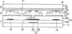
图1是表示构成实施方式1的液晶显示装置的显示面的像素的俯视示意图。FIG. 1 is a schematic plan view showing pixels constituting a display surface of a liquid crystal display device according to Embodiment 1. FIG.
图2是表示实施方式1的液晶显示装置的基板结构,是沿着图1的A-B线的剖视示意图。2 is a schematic cross-sectional view showing the substrate structure of the liquid crystal display device according to Embodiment 1 along line A-B in FIG. 1 .
图3是表示构成实施方式2的液晶显示装置的显示面的像素的俯视示意图。3 is a schematic plan view showing pixels constituting a display surface of a liquid crystal display device according to
图4表示在实施方式2的液晶显示装置中形成有导电性桥的区域的结构,是沿着图3的C-D线的剖视示意图。FIG. 4 shows the structure of a region where a conductive bridge is formed in the liquid crystal display device according to
图5是表示构成实施方式3的液晶显示装置的显示面的像素的俯视示意图。5 is a schematic plan view showing pixels constituting a display surface of a liquid crystal display device according to
图6是表示构成实施方式4的液晶显示装置的显示面的像素的俯视示意图。6 is a schematic plan view showing pixels constituting a display surface of a liquid crystal display device according to Embodiment 4. FIG.
图7是表示构成实施方式5的液晶显示装置的显示面的像素的俯视示意图。7 is a schematic plan view showing pixels constituting a display surface of a liquid crystal display device according to Embodiment 5. FIG.
图8是表示构成实施方式6的液晶显示装置的显示面的像素的俯视示意图。8 is a schematic plan view showing pixels constituting a display surface of a liquid crystal display device according to Embodiment 6. FIG.
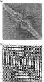
图9是表示参考例1的液晶显示装置中的液晶分子的响应特性的图,表示从电压施加开始经过10msec后的图。另外,(a)是狭缝和液晶分子的放大图,(b)是将(a)进一步放大的图。9 is a graph showing the response characteristics of liquid crystal molecules in the liquid crystal display device of Reference Example 1, showing the graph after 10 msec has elapsed from voltage application. In addition, (a) is an enlarged view of slits and liquid crystal molecules, and (b) is a further enlarged view of (a).
图10是表示参考例1的液晶显示装置中的液晶分子的响应特性的图,表示从电压施加开始经过100msec后的图。另外,(a)是狭缝和液晶分子的放大图,(b)是将(a)进一步放大的图。10 is a graph showing the response characteristics of liquid crystal molecules in the liquid crystal display device of Reference Example 1, showing the graph after 100 msec has elapsed from voltage application. In addition, (a) is an enlarged view of slits and liquid crystal molecules, and (b) is a further enlarged view of (a).
图11是表示参考例1的液晶显示装置中的液晶分子的响应特性的图,表示从电压施加开始经过500msec后的图。另外,(a)是狭缝和液晶分子的放大图,(b)是将(a)进一步放大的图。11 is a graph showing the response characteristics of liquid crystal molecules in the liquid crystal display device of Reference Example 1, showing the graph after 500 msec has elapsed from voltage application. In addition, (a) is an enlarged view of slits and liquid crystal molecules, and (b) is a further enlarged view of (a).
图12是表示参考例2的液晶显示装置中的液晶分子的响应特性的图,表示从电压施加开始经过10msec后的图。另外,(a)是狭缝和液晶分子的放大图,(b)是将(a)进一步放大的图。12 is a graph showing the response characteristics of liquid crystal molecules in the liquid crystal display device of Reference Example 2, showing the graph after 10 msec has elapsed from voltage application. In addition, (a) is an enlarged view of slits and liquid crystal molecules, and (b) is a further enlarged view of (a).
图13是表示参考例2的液晶显示装置中的液晶分子的响应特性的图,表示从电压施加开始经过100msec后的图。另外,(a)是狭缝和液晶分子的放大图,(b)是将(a)进一步放大的图。13 is a graph showing the response characteristics of liquid crystal molecules in the liquid crystal display device of Reference Example 2, showing the graph after 100 msec has elapsed from voltage application. In addition, (a) is an enlarged view of slits and liquid crystal molecules, and (b) is a further enlarged view of (a).
图14是表示参考例2的液晶显示装置中的液晶分子的响应特性的图,表示从电压施加开始经过500msec后的图。另外,(a)是狭缝和液晶分子的放大图,(b)是将(a)进一步放大的图。14 is a graph showing the response characteristics of liquid crystal molecules in the liquid crystal display device of Reference Example 2, showing the graph after 500 msec has elapsed from voltage application. In addition, (a) is an enlarged view of slits and liquid crystal molecules, and (b) is a further enlarged view of (a).
图15是表示实施例2~6的液晶显示装置中的液晶分子的响应特性的图,表示从电压施加开始经过10msec后的图。另外,(a)是狭缝和液晶分子的放大图,(b)是将(a)进一步放大的图。15 is a graph showing the response characteristics of liquid crystal molecules in the liquid crystal display devices of Examples 2 to 6, showing the graph after 10 msec has elapsed from voltage application. In addition, (a) is an enlarged view of slits and liquid crystal molecules, and (b) is a further enlarged view of (a).
图16是表示实施例2~6的液晶显示装置中的液晶分子的响应特性的图,表示从电压施加开始经过100msec后的图。另外,(a)是狭缝和液晶分子的放大图,(b)是将(a)进一步放大的图。16 is a graph showing the response characteristics of liquid crystal molecules in the liquid crystal display devices of Examples 2 to 6, showing the graph after 100 msec has elapsed from voltage application. In addition, (a) is an enlarged view of slits and liquid crystal molecules, and (b) is a further enlarged view of (a).
图17是表示实施例2~6的液晶显示装置中的液晶分子的响应特性的图,表示从电压施加开始经过500msec后的图。另外,(a)是狭缝和液晶分子的放大图,(b)是将(a)进一步放大的图。17 is a graph showing the response characteristics of liquid crystal molecules in the liquid crystal display devices of Examples 2 to 6, showing the graph after 500 msec has elapsed from voltage application. In addition, (a) is an enlarged view of slits and liquid crystal molecules, and (b) is a further enlarged view of (a).
图18是表示参考例1、参考例2和实施例2~6的液晶显示装置的随着时间变化的亮度的变化的图表。18 is a graph showing changes in luminance over time for the liquid crystal display devices of Reference Example 1, Reference Example 2, and Examples 2 to 6. FIG.
符号说明Symbol Description
1:阵列基板1: Array substrate
2:彩色滤光片基板2: Color filter substrate
3:液晶层3: Liquid crystal layer
10:像素电极的角落部10: Corner portion of the pixel electrode
11、21:玻璃基板11, 21: glass substrate
12:像素驱动用配线12: Wiring for pixel drive
13:TFT、薄膜晶体管13: TFT, thin film transistor
14:层间绝缘膜14: Interlayer insulating film
14a:第一层间绝缘膜14a: First interlayer insulating film
14b:第二层间绝缘膜14b: Second interlayer insulating film
15:像素电极15: Pixel electrode
16:接触孔16: Contact hole
17:狭缝17: Slit
18:角落部遮光性金属膜(角落部遮光部件)18: Corner light-shielding metal film (corner light-shielding member)
19:导电性桥19: Conductive bridge
22:彩色滤光片层22: Color filter layer
23:共用电极23: common electrode
24:肋(电介质突起物)24: rib (dielectric protrusion)
31:液晶分子31: liquid crystal molecules
41:栅极配线41: Gate wiring
42:源极配线42: Source wiring
43:CS配线、保持电容配线(主遮光部件、角落部遮光部件)43: CS wiring, holding capacitor wiring (main light-shielding parts, corner light-shielding parts)
44:漏极引出配线(主遮光部件、角落部遮光部件)44: Drain Lead Wiring (Main Shading Part, Corner Shading Part)
具体实施方式Detailed ways
以下举实施方式为例,参照附图对本发明进行更详细的说明。但本发明并不仅限定于这些实施方式。The following embodiments will be taken as examples to describe the present invention in more detail with reference to the accompanying drawings. However, the present invention is not limited to these embodiments.
(实施方式1)(Embodiment 1)
图1是表示构成实施方式1的液晶显示装置的显示面的像素的俯视示意图。如图1所示,构成实施方式1的液晶显示装置的显示面的像素为矩形,呈矩阵状或三角形状多个配置从而构成1个显示面。在实施方式1中,像素的数量没有特别限定。FIG. 1 is a schematic plan view showing pixels constituting a display surface of a liquid crystal display device according to Embodiment 1. FIG. As shown in FIG. 1 , pixels constituting the display surface of the liquid crystal display device according to Embodiment 1 are rectangular, and a plurality of pixels are arranged in a matrix or triangular shape to constitute one display surface. In Embodiment 1, the number of pixels is not particularly limited.
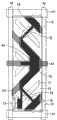
图2表示实施方式1的液晶显示装置的基板结构,是沿着图1的A-B线的剖视示意图。如图2所示,实施方式1的液晶显示装置具备由阵列基板1和彩色滤光片基板2构成的一对基板、和由这一对基板夹持的液晶层3,它们向着显示面依次配置有阵列基板1、液晶层3和彩色滤光片基板2。液晶层3由具有负的介电各向异性的向列液晶构成,在阵列基板1和彩色滤光片基板2的液晶层3一侧的表面形成有垂直取向膜。因此,实施方式1是VA模式的一个方式,在无电压施加时液晶分子31与各基板垂直地取向。另外,在阵列基板1的更靠背面一侧和彩色滤光片基板2的更靠显示面一侧,分别设置有偏光板,它们按照吸收轴相互正交的方式配置。由此,实施方式1的液晶显示装置在无电压施加时成为黑显示,即为所谓的常黑模式的结构。FIG. 2 shows the substrate structure of the liquid crystal display device according to Embodiment 1, and is a schematic cross-sectional view taken along line A-B in FIG. 1 . As shown in FIG. 2 , the liquid crystal display device of Embodiment 1 includes a pair of substrates composed of an array substrate 1 and a
对彩色滤光片基板2进行说明。如图2所示,在实施方式1中,彩色滤光片基板2具备向着液晶层3依次层叠的玻璃基板21、彩色滤光片层22、共用电极23、和在从显示面一侧看时为线状的电介质突起物(以下,将这样的电介质突起物称为“肋”)24。彩色滤光片层22由有机树脂构成,由包含红、绿、蓝等颜料的材料构成各颜色。另外,在各颜色之间形成有由包含黑的颜料的材料构成的黑矩阵,能够抑制各颜色的混色、漏光等。共用电极23形成在彩色滤光片基板2的一面,能够与阵列基板1所具备的像素电极15一起对液晶层3施加一定的电压。作为共用电极23的材料,能够合适地使用ITO(Indium Tin Oxide:铟锡氧化物)、IZO(Indium Zinc Oxide:铟锌氧化物)等具有透明性的金属氧化膜。肋24由具有绝缘性的有机树脂构成,能够使与肋24相邻的液晶分子31向着肋24取向。另外,在实施方式1中,肋24是向着液晶层3的凸的锤状,剖面形状为三角形,但只要向着液晶层突出即可,也可以为柱状,或具有曲面的山状。另外,作为剖面形状的例子,此处还能够列举长方形、梯形、描绘出抛物线的山形等。The
对阵列基板1进行说明。如图2所示,在实施方式1中,阵列基板1具备向着液晶层3依次层叠的玻璃基板11、像素驱动用配线12和作为开关元件的薄膜晶体管(TFT)13、层间绝缘膜14、以及像素电极15。在实施方式1中,像素驱动用配线12相当于栅极配线41、源极配线42、保持电容配线(CS配线)43、从TFT延伸形成的漏极引出配线44等。另外,如图1所示,在实施方式1的阵列基板1中,栅极配线41和源极配线42按照分别正交的方式配置有多根,在各交点配置有TFT13。栅极配线41能够对TFT13供给栅极信号,源极配线42能够经由TFT13对像素电极15供给源极信号。在由栅极配线41和源极配线42包围的区域,隔着由第一层间绝缘膜14a和第二层间绝缘膜14b构成的层间绝缘膜14,矩形的像素电极15配置为矩阵状,1个像素电极15构成1个像素。在实施方式1中,漏极引出配线44从TFT13延伸到达像素中央部,在像素中央部,漏极引出配线44和像素电极15通过接触孔16连接。这样,对1个像素配置有1个TFT13,各像素被分别控制。另外,接触孔16形成在第二层间绝缘膜14b内。另外,在本实施方式中,CS配线43按照穿过像素15的中央的方式与栅极配线41平行地配置。该CS配线43按照隔着第一层间绝缘层14a与漏极引出配线44重叠的方式设置,在漏极引出配线44与CS配线43之间能够形成一定的静电电容。The array substrate 1 will be described. As shown in FIG. 2 , in Embodiment 1, the array substrate 1 includes a
如图1所示,在实施方式1中,在彩色滤光片基板2设置有多根用于使液晶分子31在一定的方向取向的肋24。肋24在从显示面一侧看时为线状,多根肋24按照与像素电极15重叠的方式形成。更详细地说,在实施方式1中,肋24配置在与像素电极15的各边成约45°的角度的方向上。另外,多根肋24中的一个具有弯曲部,在以像素单位俯视时为V字状。另外,多根肋24的另外一个为直线状,并且配置在像素电极15的角落部。在图1中,以圆虚线表示的部分是像素电极15的角落部10。另外,在实施方式1中,肋24也可以在一部分具有分支部,并且也可以相对于一边形成在水平方向或垂直方向上。因此,在实施方式1中,作为每一根肋24的形状,例如在从显示面一侧看时为直线状、U字状、V字状、W字状或它们组合而成的形状。As shown in FIG. 1 , in Embodiment 1, a plurality of
如图1所示,在实施方式1中,在阵列基板1所具备的像素电极15设置有多根用于使液晶分子31在一定的方向取向的狭缝17。狭缝17在从显示面一侧看时为线状,与肋24平行,并与相邻的肋24等间隔地形成。另外,多根狭缝24中的一个具有弯曲部,在以像素单位俯视时为V字状。As shown in FIG. 1 , in Embodiment 1, a plurality of
因为液晶层3中的液晶分子31分别向着肋24和狭缝17取向,所以通过像这样在相对于像素电极15的各边倾斜的方向上设置肋24和狭缝17,能够实现广视野角。因此,实施方式1的液晶显示装置为所谓的MVA方式。Since the
在实施方式1中的阵列基板1上,按照与配置在像素电极15的角落部10的直线状肋24重叠的方式设置有遮光性金属膜18(以下称角落部遮光性金属膜)作为遮光部件(角落部遮光部件)。作为角落部遮光性金属膜,能够列举铝(Al)、银(Ag)、氮化钽(TaN)、氮化钛(TiN)、氮化钼(MoN)等。另外,按照与配置在像素电极的中央部的V字状的肋重叠的方式,延伸设置有漏极引出配线44作为遮光部件(主遮光部件)。因此,按照与配置在像素电极15的角落部10的肋24重叠的方式设置的角落部遮光性金属膜18为直线状,按照与配置在像素电极15的中央部的肋24重叠的方式设置的漏极引出配线44,进一步按照与CS配线43一部分重叠的方式配置,因而整体为W字状。漏极引出配线44能够由遮光性金属构成,作为遮光性部件能够对与肋24重叠的区域进行遮光。作为这样的遮光部件18、44的形成方法,可列举例如利用溅射法等在整个面形成金属膜后在希望的区域形成抗蚀剂,在掩膜曝光后经过显影、蚀刻、抗蚀剂剥离等处理进行图案化的方法。另外,在实施方式1中,遮光部件也可以不使用形成在阵列基板1上的金属膜,而使用例如设置于彩色滤光片基板2的黑矩阵。On the array substrate 1 in Embodiment 1, a light-shielding metal film 18 (hereinafter referred to as a corner light-shielding metal film) is provided as a light-shielding member so as to overlap with the
以上,通过像实施方式1那样在与肋重叠的区域设置遮光部件,能够防止由于在肋的影响下液晶分子的取向性与其它区域不同而在黑显示时产生漏光,能够提高对比度。特别是,在实施方式1中,除像素电极15的中央部以外,按照能够对透过配置于像素电极15的角落部10的肋24的光也进行遮光的方式设置有遮光部件,所以能够得到高对比度。As described above, by providing a light-shielding member in the region overlapping the ribs as in Embodiment 1, it is possible to prevent light leakage during black display due to the difference in orientation of liquid crystal molecules under the influence of the ribs, and to improve contrast. In particular, in Embodiment 1, a light shielding member is provided so as to shield light transmitted through the
另外,在实施方式1中,设置在像素电极15的中央部的保持电容配线43和设置在像素电极15的角落部10的角落部遮光性金属膜18的宽度,设置得比肋24的宽度大。因此,即使在将阵列基板1和彩色滤光片基板2粘在一起时产生对准错位的情况下,也能够没问题地进行遮光,提高对比度改善的可信赖性。In Embodiment 1, the width of the
实施方式1的液晶显示装置能够作为透过型的液晶显示装置使用,也能够作为半透过型的液晶显示装置使用。如果是透过型的液晶显示装置,只需在像这样形成的阵列基板1的更靠背面一侧设置背光源等光源即可。The liquid crystal display device of Embodiment 1 can be used as a transmissive liquid crystal display device, and can also be used as a transflective liquid crystal display device. If it is a transmissive liquid crystal display device, it is only necessary to install a light source such as a backlight on the rear side of the array substrate 1 formed in this way.
如果是半透过型的液晶显示装置,在像这样形成的阵列基板1的更靠背面一侧设置背光源等光源,并对各个偏光板配置λ/4相位差板。这时λ/4相位差板设置在各偏光板的液晶层一侧。这样一来,能够将由于偏光板而成为直线偏振光的透过光变换为圆偏振光,能够成为进行透过显示和反射显示两者的显示的形态,其中,透过显示将从背光源等光源出射的光作为显示光使用,反射显示使外来光在漏极引出配线反射而将该光作为显示光使用。In the case of a transflective liquid crystal display device, a light source such as a backlight is provided on the rear side of the array substrate 1 thus formed, and a λ/4 retardation plate is arranged for each polarizer. In this case, the λ/4 retardation plate is disposed on the liquid crystal layer side of each polarizing plate. In this way, the transmitted light that is linearly polarized by the polarizing plate can be converted into circularly polarized light, and it is possible to implement both transmissive display and reflective display. Light emitted from the light source is used as display light, and in reflective display, external light is reflected on the drain lead-out wiring to use the light as display light.
在实施方式1中,漏极引出配线44按照具有反射光的反射面的方式形成,由此,其不仅作为对于透过肋24的光而言的遮光部件,还作为用于反射显示的反射部件发挥功能。作为具有遮光性并具有高反射性的材料,可列举铝、银。In Embodiment 1, the drain lead-
另外,在半透过型的液晶显示装置中,在反射区域设置有多间隙(multi gap)层。这是因为,在透过区域,显示光只透过液晶层1次,而与此相对,在反射区域,显示光在反射前和反射后2次透过液晶层,显示光在透过区域和反射区域产生相位差。通过仅在反射区域进行使阵列基板1的层间绝缘膜14的厚度变厚等措施,能够形成多间隙层,通过设计透过区域的液晶层的厚度为反射区域的液晶层的厚度的约2倍,能够进行相位差的补偿。In addition, in the transflective liquid crystal display device, a multi-gap layer is provided in the reflective region. This is because, in the transmission region, the display light only passes through the liquid crystal layer once, whereas in the reflection region, the display light passes through the liquid crystal layer twice before reflection and after reflection, and the display light passes through the liquid crystal layer twice in the transmission region and the reflection region. The reflective area produces a phase difference. By taking measures such as making the thickness of the
(实施方式2)(Embodiment 2)
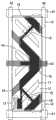
图3是表示构成实施方式2的液晶显示装置的显示面的像素的俯视示意图。如图3所示,实施方式2的液晶显示装置中像素的结构除遮光部件的形状不同以外均与实施方式1相同。因此,与实施方式1相同地,除像素电极15的中央部以外,在像素电极15的角落部10也设置用于对透过肋24的光进行遮光的遮光部件,所以能够得到高对比度。另外,设置在像素电极15的中央部的保持电容配线43和设置在像素电极15的角落部10的角落部遮光性金属膜18的宽度,设置得比肋24的宽度大,因此,即使在将阵列基板1和彩色滤光片基板2粘在一起时产生对准错位的情况下,也能够没问题地进行遮光,提高对比度改善的可信赖性。3 is a schematic plan view showing pixels constituting a display surface of a liquid crystal display device according to
另外,在实施方式2中,按照与肋24重叠的方式设置的漏极引出配线44和角落部遮光性金属膜18,分别经由导电性桥19电连接。在实施方式2中,导电性桥19从角落部遮光性金属膜18的一个末端延伸而出。并且,导电性桥19设置在与肋24和狭缝17正交的方向上。因此,利用实施方式2,不再出现只有角落部遮光性金属膜18孤立的情况,即使产生预测外的静电,该静电也会通过漏极引出配线44而消除,显示品质变得稳定。Further, in
图4表示在实施方式2的液晶显示装置中形成有导电性桥的区域的结构,是沿着图3的C-D线的剖视示意图。如图4所示,在实施方式2中,导电性桥19形成在第一层间绝缘膜14a与第二层间绝缘膜14b之间的层,形成在与形成有像素电极15的层不同的层。另外,如图3所示,导电性桥19按照横穿形成在像素电极15的狭缝17的方式设置。通过这样的结构,能够利用产生在导电性桥19的周围的电场泄漏的影响,使狭缝17的周围的电位变化,能够防止伴随狭缝17过长或宽度过窄而产生的响应速度的降低。FIG. 4 shows the structure of a region where a conductive bridge is formed in the liquid crystal display device according to
(实施方式3)(Embodiment 3)
图5是表示构成实施方式3的液晶显示装置的显示面的像素的俯视示意图。如图5所示,实施方式3的液晶显示装置中像素的结构除遮光部件的形状不同以外均与实施方式1相同。因此,与实施方式1相同地,除像素电极15的中央部以外,在像素电极15的角落部10也设置有用于对透过肋24的光进行遮光的遮光部件,所以能够得到高对比度。另外,设置在像素电极15的中央部的保持电容配线44和设置在像素电极15的角落部10的角落部遮光性金属膜18的宽度,设置得比肋24的宽度大,因此,即使在将阵列基板1和彩色滤光片基板2粘在一起时产生对准错位的情况下,也能够没问题地进行遮光,提高对比度改善的可信赖性。5 is a schematic plan view showing pixels constituting a display surface of a liquid crystal display device according to
另外,在实施方式3中,与实施方式2相同地,按照与肋24重叠的方式设置的漏极引出配线44和角落部遮光性金属膜18,分别经由导电性桥19电连接。在实施方式3中,导电性桥19从角落部遮光性金属膜18的中央部分延伸而出。并且,导电性桥19设置在与肋24和狭缝17正交的方向上。因此,利用实施方式3,与实施方式2相同地,不再出现只有角落部遮光性金属膜18孤立的情况,即使产生预测外的静电,该静电也会通过漏极引出配线44而消除,显示品质变得稳定。In addition, in
在实施方式3中,导电性桥19隔着层间绝缘膜14设置在与像素电极15不同的层,并横穿形成在像素电极15的狭缝17,由此,与实施方式2相同地,能够利用产生在该导电性桥19的周围的电场泄漏的影响,使狭缝17的周围的电位变化,例如,能够防止伴随狭缝17过长或宽度过窄而产生的响应速度的降低。In the third embodiment, the
在实施方式3中,导电性桥19与实施方式2不同,配置成包含狭缝17的中央。因此,能够有效地分割狭缝17,响应速度改善的可信赖性得到提高。In
(实施方式4)(Embodiment 4)
图6是表示构成实施方式4的液晶显示装置的显示面的像素的俯视示意图。如图6所示,实施方式4的液晶显示装置中像素的结构除遮光部件的形状不同以外均与实施方式1相同。不过,在实施方式4中,角落部遮光性金属膜18只配置在像素电极15的4个角落部中右上的角落部10,能够根据设计适当地变更形成在角落部的遮光性金属膜的数量。在这样的方式中,除像素电极15的中央部以外,在像素电极15的1个角落部10也设置用于对透过肋24的光进行遮光的遮光部件,所以能够得到高对比度。另外,设置在像素电极15的中央部的保持电容配线44和设置在像素电极15的角落部10的角落部遮光性金属膜18的宽度,设置得比肋24的宽度大,因此,即使在将阵列基板1和彩色滤光片基板2粘在一起时产生对准错位的情况下,也能够没问题地进行遮光,提高对比度改善的可信赖性。6 is a schematic plan view showing pixels constituting a display surface of a liquid crystal display device according to Embodiment 4. FIG. As shown in FIG. 6 , the configuration of pixels in the liquid crystal display device of Embodiment 4 is the same as that of Embodiment 1 except for the shape of the light shielding member. However, in Embodiment 4, the light-shielding
另外,在实施方式4中,与实施方式2相同地,按照与肋24重叠的方式设置的漏极引出配线44和设置在角落部10的角落部遮光性金属膜18,分别经由导电性桥19电连接。在实施方式4中,导电性桥19从设置于角落部10的线状的角落部遮光性金属膜18的中央部分延伸而出。并且,导电性桥19设置在与肋24和狭缝17正交的方向上。因此,利用实施方式4,与实施方式2相同地,不再出现只有设置在角落部10的角落部遮光性金属膜18孤立的情况,即使产生预测外的静电,该静电也会通过漏极引出配线44而消除,显示品质变得稳定。In addition, in the fourth embodiment, similar to the second embodiment, the drain lead-
在实施方式4中,导电性桥19隔着层间绝缘膜14设置在与像素电极15不同的层,并横穿形成于像素电极15的狭缝17,由此,与实施方式2相同地,能够利用产生在该导电性桥19的周围的电场泄漏的影响,使狭缝17的周围的电位变化,能够防止伴随狭缝17过长或宽度过窄而产生的响应速度的降低。In the fourth embodiment, the
在实施方式4中,导电性桥19与实施方式3相同地,配置成包含狭缝17的中央。因此,能够有效地分割狭缝17,响应速度改善的可信赖性得到提高。In the fourth embodiment, the
(实施方式5)(Embodiment 5)
图7是表示构成实施方式5的液晶显示装置的显示面的像素的俯视示意图。如图7所示,实施方式5的液晶显示装置中像素的结构除遮光部件的形状不同以外均与实施方式1相同。在实施方式5中,遮光部件使用漏极引出配线44与CS配线43两者。并且,CS配线43大致整体与漏极引出配线44重叠。即CS配线43也为线状并在一部分具有弯曲部,在从显示面看时为W字状。按照形成在漏极引出配线44与CS配线43之间的静电电容的大小,能够适当地使用这样的设计。在实施方式5中,与实施方式1相同地,除像素电极15的中央部以外,在像素电极15的角落部10也设置用于对透过肋24的光进行遮光的遮光部件,所以能够得到高对比度。另外,设置在像素电极15的中央部的保持电容配线44和CS配线43,以及设置在像素电极15的角落部10的角落部遮光性金属膜18的宽度,设置得比肋24的宽度大,因此,即使在将阵列基板1和彩色滤光片基板2粘在一起时产生对准错位的情况下,也能够没问题地进行遮光,提高对比度改善的可信赖性。7 is a schematic plan view showing pixels constituting a display surface of a liquid crystal display device according to Embodiment 5. FIG. As shown in FIG. 7 , the configuration of pixels in the liquid crystal display device of the fifth embodiment is the same as that of the first embodiment except for the shape of the light shielding member. In Embodiment 5, both the
另外,在实施方式5中,与实施方式2相同地,按照与肋24重叠的方式设置的漏极引出配线44和角落部遮光性金属膜18,分别经由导电性桥19电连接。在实施方式5中,导电性桥19从角落部遮光性金属膜18的中央部分延伸而出。并且,导电性桥19设置在与肋24和狭缝17正交的方向上。因此,利用实施方式5,与实施方式2相同地,不再出现只有角落部遮光性金属膜18孤立的情况,即使产生预测以外的静电,该静电也会通过漏极引出配线44而消除,显示品质变得稳定。In addition, in Embodiment 5, similarly to
在实施方式5中,导电性桥19隔着层间绝缘膜14设置在与像素电极15不同的层,并横穿形成于像素电极15的狭缝17,由此,与实施方式2相同地,能够利用在该导电性桥19的周围产生的电场泄漏的影响,使狭缝17的周围的电位变化,例如,能够防止伴随狭缝17过长或宽度过窄而产生的响应速度的降低。In the fifth embodiment, the
在实施方式5中,导电性桥19与实施方式3相同地,配置成包含狭缝17的中央。因此,能够有效地分割狭缝17,响应速度改善的可信赖性得到提高。In the fifth embodiment, the
在实施方式5中,CS配线43在像素电极15的中央部以外也宽度较宽地形成,所以与实施方式1~4相比,能够在像素电极15的中央部减少CS配线43的在像素电极15的中央部以外也宽度较宽地形成的量的面积,能够提高开口率。像实施方式5这样,通过使用CS配线43和漏极引出配线44作为遮光部件,能够像这样地使设计高效化,能够提高显示品质。In Embodiment 5, the
(实施方式6)(Embodiment 6)
图8是表示构成实施方式6的液晶显示装置的显示面的像素的俯视示意图。如图8所示,在实施方式6的液晶显示装置中像素的结构除遮光部件的形状不同以外均与实施方式1相同。另外,在实施方式6中,遮光部件使用漏极引出配线44和CS配线43两者这一点与实施方式5相同,但与实施方式5不同的是,CS配线43并不与全部漏极引出配线44重叠。不与设置于像素电极15的角落部10的角落部遮光性金属膜18和导电性桥19重叠。按照形成在漏极引出配线44与CS配线43之间的静电电容的大小,能够适当地采用这样的设计。在实施方式6中,与实施方式1相同地,除像素电极15的中央部以外,在像素电极15的角落部10也设置用于对透过肋24的光进行遮光的遮光部件,所以能够得到高对比度。另外,设置于像素电极15的中央部的保持电容配线44和CS配线43,以及设置于像素电极15的角落部10的角落部遮光性金属膜18的宽度,设置得比肋24的宽度大,因此,即使在将阵列基板1和彩色滤光片基板2粘在一起时产生对准错位的情况下,也能够没问题地进行遮光,提高对比度改善的可信赖性。8 is a schematic plan view showing pixels constituting a display surface of a liquid crystal display device according to Embodiment 6. FIG. As shown in FIG. 8 , the configuration of pixels in the liquid crystal display device of Embodiment 6 is the same as that of Embodiment 1 except for the shape of the light shielding member. In addition, in Embodiment 6, the point that both the drain lead-
另外,在实施方式6中,与实施方式2相同地,按照与肋24重叠的方式设置的漏极引出配线44和角落部遮光性金属膜18,分别经由导电性桥19电连接。在实施方式6中,导电性桥19从角落部遮光性金属膜18的中央部分延伸而出。并且,导电性桥19设置在与肋24和狭缝17正交的方向上。因此,利用实施方式6,与实施方式2相同地,不再出现只有设置在角落部10的角落部遮光性金属膜18孤立的情况,即使产生预测外的静电,该静电也会通过漏极引出配线44而消除,显示品质变得稳定。In Embodiment 6, similarly to
在实施方式6中,导电性桥19隔着层间绝缘膜14设置在与像素电极15不同的层,并横穿形成在像素电极15的狭缝17,由此,与实施方式2相同地,能够利用产生在该导电性桥19的周围的电场泄漏的影响,使狭缝17的周围的电位变化,例如,能够防止伴随狭缝17过长或宽度过窄而产生的响应速度的降低。In the sixth embodiment, the
在实施方式6中,导电性桥19与实施方式3相同地,配置成包含狭缝17的中央。因此,能够有效地分割狭缝17,响应速度改善的可信赖性得到提高。In the sixth embodiment, the
在实施方式6中,CS配线43在像素电极15的中央部以外也宽度较宽地形成,所以与实施方式1~4相比,能够在像素电极15的中央部减少CS配线43的在像素电极15的中央部以外也宽度较宽地形成的量的面积,能够提高开口率。像实施方式6这样,通过使用CS配线43和漏极引出配线44作为遮光部件,能够像这样地使设计高效化,能够提高显示品质。In Embodiment 6, the
(评价试验)(evaluation test)
对于利用导电性桥使形成在本发明的像素电极的狭缝的电位变化从而改善响应特性的方式,为了调查其改善效果,进行以下模拟进而评价。The following simulations were performed and evaluated in order to investigate the effect of improving response characteristics by changing the potential of the slit formed in the pixel electrode of the present invention by using a conductive bridge.
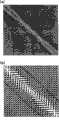
首先,作为参考例1的液晶显示装置,假定像素电极的狭缝宽度为9μm,作为参考例2的液晶显示装置,假定像素电极的狭缝宽度为5μm,对位于这些狭缝内和狭缝周围的液晶分子的取向行为进行模拟。First, as the liquid crystal display device of reference example 1, it is assumed that the slit width of the pixel electrode is 9 μm, and as the liquid crystal display device of reference example 2, the slit width of the pixel electrode is assumed to be 5 μm, and the slits located in and around these slits The orientation behavior of liquid crystal molecules was simulated.
图9~11是表示参考例1的液晶显示装置中的液晶分子的响应特性的图,图9表示从电压施加开始经过10msec后的图,图10表示从电压施加开始经过100msec后的图,图11表示从电压施加开始经过500msec后的图。另外,图9(a)~图11(a)是狭缝和液晶分子的放大图,图9(b)~图11(b)是将图9(a)~图11(a)分别进一步放大的图。另外,图9~图11中的黑线表示等电位线。9 to 11 are graphs showing the response characteristics of the liquid crystal molecules in the liquid crystal display device of Reference Example 1. FIG. 9 shows a graph after 10 msec from voltage application, and FIG. 10 shows a graph after 100 msec from voltage application. 11 shows a graph after 500 msec has elapsed from the voltage application. In addition, Figures 9(a) to 11(a) are enlarged views of slits and liquid crystal molecules, and Figures 9(b) to 11(b) are further enlarged views of Figures 9(a) to 11(a) diagram. In addition, the black lines in FIGS. 9 to 11 indicate equipotential lines.
如图9~图11所示,在狭缝宽为9μm(参考例1)时,位于狭缝内的液晶分子在与像素电极面垂直的方向上取向,但位于狭缝的边界线周围的液晶分子从紧接取向开始后(经过10msec后)开始,在相对于像素电极面水平的方向并与狭缝的长度方向成直角的方向上倒下,经过100msec、500msec的时间后该倾向也不改变。As shown in Figures 9 to 11, when the slit width is 9 μm (Reference Example 1), the liquid crystal molecules located in the slit are aligned in the direction perpendicular to the pixel electrode surface, but the liquid crystal molecules located around the boundary line of the slit Immediately after the start of alignment (after 10 msec), the molecules fall in a direction horizontal to the pixel electrode surface and at right angles to the longitudinal direction of the slit, and this tendency does not change even after 100 msec and 500 msec. .
图12~14是表示参考例2的液晶显示装置中的液晶分子的响应特性的图,图12表示从电压施加开始经过10msec后的图,图13表示从电压施加开始经过100msec后的图,图14表示从电压施加开始经过500msec后的图。另外,图12(a)~图14(a)是狭缝和液晶分子的放大图,图12(b)~图14(b)是将图12(a)~图14(a)分别进一步放大的图。另外,图12~图14中的黑线表示等电位线。12 to 14 are graphs showing the response characteristics of the liquid crystal molecules in the liquid crystal display device of Reference Example 2. FIG. 12 shows a graph after 10 msec from voltage application, and FIG. 13 shows a graph after 100 msec from voltage application. 14 shows a graph after 500 msec has elapsed from the voltage application. In addition, FIG. 12(a) to FIG. 14(a) are enlarged views of slits and liquid crystal molecules, and FIG. 12(b) to FIG. 14(b) are further enlarged views of FIG. 12(a) to FIG. 14(a). diagram. In addition, the black lines in FIGS. 12 to 14 indicate equipotential lines.
如图12~图14所示,在狭缝宽为5μm(参考例2)时,在紧接取向开始后(经过10msec后),除了位于狭缝的中央线上的液晶分子以外,位于狭缝内和狭缝的边界线周围的液晶分子,在相对于像素电极面水平的方向并与狭缝的长度方向成直角的方向上倒下。另外,位于狭缝的中心线上的液晶分子在与像素电极面垂直的方向上取向。因此,在随着100msec、500msec时间的经过,在相对于像素电极面倾斜的方向、并且在相对于狭缝的长度方向也倾斜的方向上倒下,最终,位于狭缝的中心线上的液晶分子在与狭缝的长度方向相同的方向、并且在相对于像素电极面倾斜的方向上取向。另外,位于狭缝内的狭缝的中心线上以外的区域的液晶分子,按照在相对于狭缝的长度方向倾斜的方向、并且在相对于像素电极面倾斜的方向上取向的方式变化。另外,在参考例2的液晶显示装置中,如图13和图14所示,在从电压施加开始100msec后和500msec后,在狭缝内的一部分,形成有一部分区域,该区域为以在与像素电极面垂直的方向上取向的液晶分子为奇点,液晶分子的取向方向相对于狭缝的长度方向相互点对称的区域,该取向方向持续到下一个奇点为止。As shown in FIGS. 12 to 14, when the slit width is 5 μm (Reference Example 2), immediately after the start of alignment (after 10 msec), except for the liquid crystal molecules located on the central line of the slit, The liquid crystal molecules in and around the boundary of the slit fall down in a direction that is horizontal to the pixel electrode surface and perpendicular to the longitudinal direction of the slit. In addition, the liquid crystal molecules located on the center line of the slit are aligned in a direction perpendicular to the pixel electrode surface. Therefore, with the elapse of 100msec and 500msec, the liquid crystal located on the center line of the slit falls down in a direction inclined to the pixel electrode surface and also in a direction inclined to the longitudinal direction of the slit. The molecules are aligned in the same direction as the longitudinal direction of the slit and in a direction inclined to the pixel electrode surface. In addition, the liquid crystal molecules located in the area other than the central line of the slit within the slit change so as to be aligned in a direction oblique to the longitudinal direction of the slit and in a direction oblique to the pixel electrode surface. In addition, in the liquid crystal display device of Reference Example 2, as shown in FIGS. 13 and 14 , after 100 msec and 500 msec from the start of voltage application, a partial region is formed in a part of the slit. The liquid crystal molecules aligned in the direction perpendicular to the pixel electrode surface are singular points, and the alignment directions of the liquid crystal molecules are point-symmetrical to each other with respect to the longitudinal direction of the slit, and this alignment direction continues until the next singular point.
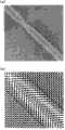
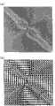
接着,对像本发明的实施例2~6那样在对像素电极的狭缝配置导电性桥时位于狭缝内和狭缝周围的液晶分子的取向行为进行模拟。在该模拟中,狭缝的宽度为5μm。图15~17是表示实施例2~6的液晶显示装置中的液晶分子的响应特性的图,图16是表示从电压施加开始经过10msec后的图,图17是表示从电压施加开始经过100msec后的图,图18表示从电压施加开始经过500msec后的图。另外,图15(a)~图17(a)是狭缝和液晶分子的放大图,图15(b)~图17(b)是将图15(a)~图17(a)分别进一步放大的图。另外,在图15~图17中黑线表示等电位线。Next, the alignment behavior of liquid crystal molecules located in and around the slits when a conductive bridge is placed in the slits of the pixel electrodes as in Examples 2 to 6 of the present invention was simulated. In this simulation, the width of the slit was 5 μm. 15 to 17 are graphs showing the response characteristics of the liquid crystal molecules in the liquid crystal display devices of Examples 2 to 6, FIG. 16 is a graph showing 10 msec from the voltage application, and FIG. 17 is 100 msec from the voltage application. 18 shows a graph after 500 msec has elapsed from the voltage application. In addition, FIG. 15(a) to FIG. 17(a) are enlarged views of slits and liquid crystal molecules, and FIG. 15(b) to FIG. 17(b) are further enlarged views of FIG. 15(a) to FIG. 17(a). diagram. In addition, in FIGS. 15 to 17 , black lines indicate equipotential lines.
如图15~17所示,在实施例2~6的情况下,沿着狭缝的形状形成的等电位线以形成有导电性桥的位置为边界分别分离。另外,在这些等电位线的边界,在狭缝的中心线与导电性桥的中心线的交点产生固定的液晶取向的奇点,以该奇点为中心,液晶分子的取向性具有对称的形状。以下进行更详细的说明。As shown in FIGS. 15 to 17 , in the cases of Examples 2 to 6, the equipotential lines formed along the shape of the slit are respectively separated at the boundary where the conductive bridge is formed. In addition, at the boundary of these equipotential lines, a singular point of fixed liquid crystal orientation is generated at the intersection point of the center line of the slit and the center line of the conductive bridge, and the orientation of the liquid crystal molecules has a symmetrical shape around the singular point. . A more detailed description will be given below.
如图15~17所示,位于形成有导电性桥的区域以外的区域的液晶分子的取向方向的变化,与图12~图14所示的参考例2时相同。另一方面,在导电性桥的中心线与狭缝的中心线交叉的地点,形成有以在与像素电极面垂直的方向上取向的液晶分子为中心的液晶分子的奇点,以该奇点为中心,表示出相互对称的取向性的液晶分子排列在其周围。As shown in FIGS. 15 to 17 , changes in the alignment directions of liquid crystal molecules located in regions other than the regions where the conductive bridges are formed are the same as those in Reference Example 2 shown in FIGS. 12 to 14 . On the other hand, at the point where the center line of the conductive bridge intersects the center line of the slit, a singular point of liquid crystal molecules centered on liquid crystal molecules aligned in a direction perpendicular to the pixel electrode surface is formed, and the singular point As a center, liquid crystal molecules exhibiting mutual symmetric orientation are arranged around it.
具体而言,首先,在紧接着电压施加后(经过10msec后),以奇点为中心,在狭缝的长度方向上,液晶分子沿着狭缝的中心线在相对于像素电极面水平的方向上排列,此外,在导电性桥的长度方向上,液晶分子沿着导电性桥的中心线在相对于像素电极面水平的方向上排列。因为狭缝的长度方向与导电性桥的长度方向各自正交,所以狭缝的中心线上的液晶分子和导电性桥的中心线上的液晶分子整体形成倾斜的十字型。另外,在狭缝的中心线上和导电性桥的中心线上以外的区域,液晶分子以一定的长度按照在相对于狭缝的中心线和导电性桥的中心线分别倾斜的方向(在本实施方式中为像素电极的短边和长边方向)、并且以奇点为中心相互对称的方式排列。这样,位于狭缝的中心线上和导电性桥的中心线上以外的区域的液晶分子,按照整体具有所谓卍型(风车型)取向性的方式排列,其中,卍型是指,以导电性桥的中心线和狭缝的长度的中心线交差的地点为拐点的三次曲线相互正交地配置的方式。另外,对于该卍型(风车型)的末端,即位于最靠近狭缝的中心线和导电性桥的中心线的区域的液晶分子,因在狭缝的长度方向和导电性桥的长度方向受到吸引,所以,位于狭缝的中心线和导电性桥的中心线附近的区域的液晶分子,按照整体具有所谓手里剑型(星型)取向性的方式排列,其中,手里剑型是指菱型在相互正交的四方向(十字方向)上排列的方式。Specifically, first, immediately after the voltage is applied (after 10 msec), with the singular point as the center, in the longitudinal direction of the slit, the liquid crystal molecules are aligned horizontally with respect to the pixel electrode surface along the center line of the slit. In addition, in the length direction of the conductive bridge, the liquid crystal molecules are arranged along the center line of the conductive bridge in a direction horizontal to the surface of the pixel electrode. Since the longitudinal direction of the slit is perpendicular to the longitudinal direction of the conductive bridge, the liquid crystal molecules on the central line of the slit and the liquid crystal molecules on the central line of the conductive bridge form an inclined cross shape as a whole. In addition, in areas other than the center line of the slit and the center line of the conductive bridge, the liquid crystal molecules are arranged in directions inclined with respect to the center line of the slit and the center line of the conductive bridge with a certain length (in this In the embodiment, the pixel electrodes are arranged symmetrically with respect to the short side and the long side direction) and centered on the singular point. In this way, the liquid crystal molecules located on the center line of the slit and the area other than the center line of the conductive bridge are arranged in a manner to have a so-called swastika (wind type) orientation as a whole. The point where the centerline of the bridge intersects with the centerline of the length of the slit is a form in which cubic curves of inflection points are arranged orthogonally to each other. In addition, for the end of the swastika (wind type), that is, the liquid crystal molecules located in the area closest to the center line of the slit and the center line of the conductive bridge, are affected by the longitudinal direction of the slit and the conductive bridge. Therefore, the liquid crystal molecules in the area near the center line of the slit and the center line of the conductive bridge are arranged in such a way that the whole has a so-called shuriken (star) orientation, wherein the shuriken refers to The way rhombuses are arranged in four directions (cross directions) orthogonal to each other.
然后,随着时间的经过,液晶分子的取向变化进一步逐渐进行,其结果为,奇点自身消失。不过,如上所述,狭缝的中心线上的液晶分子和导电性桥的中心线上的液晶分子整体维持倾斜的十字型,位于狭缝的中心线上和导电性桥的中心线上以外的区域的液晶分子维持卍型(风车型)的取向性,位于狭缝的中心线和导电性桥的中心线附近的区域的液晶分子维持手里剑型(星型)的取向性,因此,整体来说液晶分子的取向性的倾向没有大的变化。特别是,液晶分子的取向性经过100msec后和经过500msec后没有大的变化。另外,根据实施方式2~6,因为在每个狭缝与导电性桥的交点都形成有奇点,所以整体来说与参考例1和参考例2相比,奇点的数目形成得较多。Then, as time passes, the orientation change of the liquid crystal molecules progresses further gradually, and as a result, the singularity itself disappears. However, as mentioned above, the liquid crystal molecules on the central line of the slit and the liquid crystal molecules on the central line of the conductive bridge maintain an inclined cross shape as a whole, and the liquid crystal molecules located outside the central line of the slit and the central line of the conductive bridge The liquid crystal molecules in the area maintain the orientation of the swastika (wind type), and the liquid crystal molecules in the area near the center line of the slit and the center line of the conductive bridge maintain the alignment of the shuriken (star type). Therefore, the overall In other words, the tendency of the orientation of the liquid crystal molecules does not change greatly. In particular, there was no significant change in the orientation of the liquid crystal molecules after 100 msec and 500 msec. In addition, according to
根据以上说明,能够通过将导电性桥设置在狭缝的中央而有意图地形成作为取向的中心的奇点,并且,能够以该奇点为中心对液晶分子的取向设置分隔。From the above description, by disposing the conductive bridge at the center of the slit, it is possible to intentionally form a singular point as the center of alignment, and it is possible to divide the alignment of liquid crystal molecules around the singular point.
另外,根据图15~图17,在实施例2~6的情况下,狭缝内的液晶分子在紧接电压施加后(经过10msec后),在相对于像素电极面倾斜的方向、并且在相对于狭缝的长度方向也倾斜的方向上开始取向,并形成奇点。这样,100msec后取向的变化到达平衡状态,明亮度稳定。由此可知,即使在狭缝的宽度为5μm时,通过按照横穿狭缝的方式设置导电性桥,能够使到响应完结为止的时间变短,即提高响应速度,其结果为,能够使残像难以残留。In addition, according to FIGS. 15 to 17, in the case of Examples 2 to 6, the liquid crystal molecules in the slits are in the direction inclined relative to the pixel electrode surface and in the opposite direction immediately after the voltage is applied (after 10 msec). Orientation begins in a direction in which the longitudinal direction of the slit is also inclined, and a singularity is formed. In this way, after 100 msec, the change in orientation reaches an equilibrium state, and the brightness is stable. From this, it can be seen that even when the width of the slit is 5 μm, by providing the conductive bridge across the slit, the time until the response is completed can be shortened, that is, the response speed can be increased, and as a result, the afterimage can be reduced. Difficult to leave behind.
图18是表示参考例1、参考例2和实施例2~6的液晶显示装置中的随着时间变化的亮度的变化的图表。在图18中,●是参考例1(宽度9μm)的图表,▲是参考例2(宽度5μm)的图表,■是实施例2~6(宽度5μm并具有导电性的桥)的图表。18 is a graph showing changes in luminance over time in the liquid crystal display devices of Reference Example 1, Reference Example 2, and Examples 2 to 6. FIG. In FIG. 18 , ● is a graph of Reference Example 1 (width 9 μm), ▲ is a graph of Reference Example 2 (width 5 μm), and ■ is a graph of Examples 2 to 6 (bridges having a width of 5 μm and having conductivity).
由图18可知,在参考例2的液晶显示装置中,从紧接取向开始后(经过100msec后)到200msec后为止,以在与狭缝的长度方向成直角的方向上的取向为中心,所以为较明亮的显示,但随着时间的经过,取向逐渐紊乱,明亮度降低。在约500msec后取向的变化达到平衡状态,明亮度稳定。另一方面,在参考例1的液晶装置中,随着时间的经过,逐渐向相对于狭缝的长度方向成直角的方向倾斜,明亮度逐渐提高,约100msec后取向的变化达到平衡状态,明亮度稳定。像这样对参考例1和参考例2进行比较,可知参考例2中亮度的变动的上下较为强烈,到响应完结为止的时间较长。根据像这样的参考例2的液晶显示装置,与参考例1的液晶显示装置相比,显示中容易残留残像。由上可知,在使狭缝的宽度过小的情况下,即纵横比过大的情况下,显示品质的降低变得容易产生。As can be seen from FIG. 18, in the liquid crystal display device of Reference Example 2, from immediately after the start of alignment (after 100 msec elapsed) to 200 msec later, the alignment in the direction perpendicular to the longitudinal direction of the slit is the center, so It is a brighter display, but as time passes, the orientation is gradually disordered, and the brightness decreases. After about 500msec, the change in orientation reaches a balanced state, and the brightness is stable. On the other hand, in the liquid crystal device of Reference Example 1, as time passed, it gradually tilted to a direction at right angles to the longitudinal direction of the slit, and the brightness gradually increased. degree of stability. Comparing Reference Example 1 and Reference Example 2 in this way, it can be seen that in Reference Example 2, the fluctuation of luminance is relatively strong, and the time until the response is completed is long. According to the liquid crystal display device of Reference Example 2, as compared with the liquid crystal display device of Reference Example 1, afterimages tend to remain during display. As can be seen from the above, when the width of the slit is too small, that is, when the aspect ratio is too large, degradation of display quality is likely to occur.
与这样的参考例1和参考例2相对,在实施例2~6的液晶显示装置中,与参考例1一样,从紧接取向开始后(经过10msec后)到200msec后为止,以在与狭缝的长度方向成直角的方向上的取向为中心,所以成为较明亮的显示。不过,亮度的变动不像参考例1那样,整体看来在约50msec后亮度达到稳定。由此可知,根据实施例2~6的方式,约50msec后响应完结,因此,与参考例1和2相比,成为响应速度变大、残像难以残留的方式。As opposed to such Reference Example 1 and Reference Example 2, in the liquid crystal display devices of Examples 2 to 6, as in Reference Example 1, from immediately after the start of alignment (after 10 msec elapsed) to 200 msec later, the distance between the liquid crystal display devices and the narrow Since the orientation in the direction perpendicular to the longitudinal direction of the slit is the center, a brighter display is obtained. However, the luminance did not fluctuate as in Reference Example 1, and the luminance stabilized after about 50 msec as a whole. From this, it can be seen that according to the forms of Examples 2 to 6, the response is completed after about 50 msec, and therefore, compared with Reference Examples 1 and 2, the response speed is increased and afterimages are less likely to remain.
另外,本申请以2008年2月15日提出申请的日本国专利申请2008-034406号为基础,根据巴黎条约或进入国家阶段的该国法规主张优先权。作为参照,该申请的内容全部被编入本申请中。In addition, this application is based on Japanese Patent Application No. 2008-034406 filed on February 15, 2008, and claims priority under the Treaty of Paris or the laws and regulations of the country that entered the national phase. As a reference, the content of this application is incorporated in this application in its entirety.
Claims (14)
Applications Claiming Priority (3)
| Application Number | Priority Date | Filing Date | Title |
|---|---|---|---|
| JP2008034406 | 2008-02-15 | ||
| JP2008-034406 | 2008-02-15 | ||
| PCT/JP2008/069044WO2009101732A1 (en) | 2008-02-15 | 2008-10-21 | Liquid crystal display device |
Publications (2)
| Publication Number | Publication Date |
|---|---|
| CN101874226Atrue CN101874226A (en) | 2010-10-27 |
| CN101874226B CN101874226B (en) | 2012-03-28 |
Family
ID=40956770
Family Applications (1)
| Application Number | Title | Priority Date | Filing Date |
|---|---|---|---|
| CN2008801176475AExpired - Fee RelatedCN101874226B (en) | 2008-02-15 | 2008-10-21 | Liquid crystal display device |
Country Status (5)
| Country | Link |
|---|---|
| US (1) | US8305533B2 (en) |
| EP (1) | EP2241933A4 (en) |
| JP (1) | JP5068827B2 (en) |
| CN (1) | CN101874226B (en) |
| WO (1) | WO2009101732A1 (en) |
Cited By (5)
| Publication number | Priority date | Publication date | Assignee | Title |
|---|---|---|---|---|
| CN103676359A (en)* | 2013-12-19 | 2014-03-26 | 京东方科技集团股份有限公司 | Liquid crystal display panel and display device |
| CN104317115A (en)* | 2014-10-10 | 2015-01-28 | 上海中航光电子有限公司 | Pixel structure and manufacturing method thereof, array substrate, display panel and display device |
| CN106814512A (en)* | 2015-12-02 | 2017-06-09 | 株式会社日本显示器 | Liquid-crystal apparatus |
| CN107870470A (en)* | 2016-09-23 | 2018-04-03 | 三星显示有限公司 | Liquid crystal display |
| CN110780473A (en)* | 2019-10-30 | 2020-02-11 | 昆山龙腾光电股份有限公司 | Liquid crystal display device and method for manufacturing the same |
Families Citing this family (2)
| Publication number | Priority date | Publication date | Assignee | Title |
|---|---|---|---|---|
| KR102304983B1 (en)* | 2015-04-28 | 2021-09-27 | 삼성디스플레이 주식회사 | Liquid crystal display device |
| CN109581761B (en)* | 2018-12-29 | 2022-05-27 | 厦门天马微电子有限公司 | Array substrate and display device |
Family Cites Families (6)
| Publication number | Priority date | Publication date | Assignee | Title |
|---|---|---|---|---|
| TW509808B (en) | 1997-06-12 | 2002-11-11 | Sharp Kk | Liquid crystal display device |
| US7480022B2 (en) | 2003-12-10 | 2009-01-20 | Seiko Epson Corporation | Liquid crystal display device, method of manufacturing liquid crystal display device, and electronic apparatus |
| JP2006058734A (en) | 2004-08-23 | 2006-03-02 | Seiko Epson Corp | Liquid crystal display device and electronic device |
| JP2005173105A (en)* | 2003-12-10 | 2005-06-30 | Seiko Epson Corp | Liquid crystal display device and electronic device |
| JP4628801B2 (en) | 2005-01-19 | 2011-02-09 | シャープ株式会社 | Liquid crystal display device |
| WO2008129734A1 (en) | 2007-03-30 | 2008-10-30 | Sharp Kabushiki Kaisha | Liquid crystal display device |
- 2008
- 2008-10-21WOPCT/JP2008/069044patent/WO2009101732A1/enactiveApplication Filing
- 2008-10-21EPEP08872445Apatent/EP2241933A4/ennot_activeWithdrawn
- 2008-10-21USUS12/863,069patent/US8305533B2/ennot_activeExpired - Fee Related
- 2008-10-21CNCN2008801176475Apatent/CN101874226B/ennot_activeExpired - Fee Related
- 2008-10-21JPJP2009553335Apatent/JP5068827B2/ennot_activeExpired - Fee Related
Cited By (8)
| Publication number | Priority date | Publication date | Assignee | Title |
|---|---|---|---|---|
| CN103676359A (en)* | 2013-12-19 | 2014-03-26 | 京东方科技集团股份有限公司 | Liquid crystal display panel and display device |
| CN103676359B (en)* | 2013-12-19 | 2015-12-09 | 京东方科技集团股份有限公司 | A liquid crystal display and display device |
| US9658497B2 (en) | 2013-12-19 | 2017-05-23 | Boe Technology Group Co., Ltd. | Liquid crystal display and display device |
| CN104317115A (en)* | 2014-10-10 | 2015-01-28 | 上海中航光电子有限公司 | Pixel structure and manufacturing method thereof, array substrate, display panel and display device |
| CN104317115B (en)* | 2014-10-10 | 2017-11-14 | 上海中航光电子有限公司 | Dot structure and its manufacture method, array base palte, display panel and display device |
| CN106814512A (en)* | 2015-12-02 | 2017-06-09 | 株式会社日本显示器 | Liquid-crystal apparatus |
| CN107870470A (en)* | 2016-09-23 | 2018-04-03 | 三星显示有限公司 | Liquid crystal display |
| CN110780473A (en)* | 2019-10-30 | 2020-02-11 | 昆山龙腾光电股份有限公司 | Liquid crystal display device and method for manufacturing the same |
Also Published As
| Publication number | Publication date |
|---|---|
| JP5068827B2 (en) | 2012-11-07 |
| US8305533B2 (en) | 2012-11-06 |
| US20110043438A1 (en) | 2011-02-24 |
| EP2241933A4 (en) | 2011-11-16 |
| CN101874226B (en) | 2012-03-28 |
| WO2009101732A1 (en) | 2009-08-20 |
| JPWO2009101732A1 (en) | 2011-06-02 |
| EP2241933A1 (en) | 2010-10-20 |
Similar Documents
| Publication | Publication Date | Title |
|---|---|---|
| US8400603B2 (en) | Liquid crystal display panel and electronic apparatus | |
| US8018553B2 (en) | Liquid crystal display device that includes both a transmissive portion and a reflective portion | |
| US9983433B2 (en) | Transflective liquid crystal display panel comprising a phase retardation film between an over coater and a common electrode | |
| CN101874226B (en) | Liquid crystal display device | |
| JP5266574B2 (en) | Liquid crystal display | |
| US7724326B2 (en) | Liquid crystal display device comprising a shading conductive layer formed at least near an opening or cut of an electrode | |
| JP5239973B2 (en) | Liquid crystal display | |
| US20080013017A1 (en) | Liquid crystal display | |
| US20130093983A1 (en) | Liquid crystal display device | |
| JP4449958B2 (en) | FFS liquid crystal display panel | |
| CN100399120C (en) | Reflective-transmissive type liquid crystal display device | |
| CN103293789B (en) | Array substrate and manufacturing method thereof, display panel and drive method | |
| TW201508401A (en) | Display panel | |
| JPWO2009072322A1 (en) | Liquid crystal display device | |
| CN100410779C (en) | Semi-transmissive liquid crystal display panel | |
| US7982833B2 (en) | Transflective liquid crystal display panel having a plurality of apertures with a specific ratio of aperture width to aperture interval | |
| EP3040769B1 (en) | Liquid crystal display device | |
| CN101109877B (en) | Transflective LCD | |
| JP5413787B2 (en) | Liquid crystal display | |
| JP2008051846A (en) | Liquid crystal display panel of fringe field switching (ffs) mode | |
| JP5413788B2 (en) | Liquid crystal display | |
| CN102341746B (en) | Liquid crystal display device | |
| KR101192755B1 (en) | Transflective Type Liquid Crystal Display Device | |
| KR20110064168A (en) | IPS mode transflective liquid crystal display device and manufacturing method thereof | |
| JP2001147427A (en) | Liquid crystal display |
Legal Events
| Date | Code | Title | Description |
|---|---|---|---|
| C06 | Publication | ||
| PB01 | Publication | ||
| C10 | Entry into substantive examination | ||
| SE01 | Entry into force of request for substantive examination | ||
| C14 | Grant of patent or utility model | ||
| GR01 | Patent grant | ||
| CF01 | Termination of patent right due to non-payment of annual fee | Granted publication date:20120328 Termination date:20201021 | |
| CF01 | Termination of patent right due to non-payment of annual fee |