CN101872084A - Liquid crystal display device - Google Patents
Liquid crystal display deviceDownload PDFInfo
- Publication number
- CN101872084A CN101872084ACN201010166138ACN201010166138ACN101872084ACN 101872084 ACN101872084 ACN 101872084ACN 201010166138 ACN201010166138 ACN 201010166138ACN 201010166138 ACN201010166138 ACN 201010166138ACN 101872084 ACN101872084 ACN 101872084A
- Authority
- CN
- China
- Prior art keywords
- touch panel
- liquid crystal
- crystal display
- layer
- front window
- Prior art date
- Legal status (The legal status is an assumption and is not a legal conclusion. Google has not performed a legal analysis and makes no representation as to the accuracy of the status listed.)
- Granted
Links
Images


Classifications
- G—PHYSICS
- G06—COMPUTING OR CALCULATING; COUNTING
- G06F—ELECTRIC DIGITAL DATA PROCESSING
- G06F3/00—Input arrangements for transferring data to be processed into a form capable of being handled by the computer; Output arrangements for transferring data from processing unit to output unit, e.g. interface arrangements
- G06F3/01—Input arrangements or combined input and output arrangements for interaction between user and computer
- G06F3/03—Arrangements for converting the position or the displacement of a member into a coded form
- G06F3/041—Digitisers, e.g. for touch screens or touch pads, characterised by the transducing means
- G06F3/0412—Digitisers structurally integrated in a display
- G—PHYSICS
- G02—OPTICS
- G02F—OPTICAL DEVICES OR ARRANGEMENTS FOR THE CONTROL OF LIGHT BY MODIFICATION OF THE OPTICAL PROPERTIES OF THE MEDIA OF THE ELEMENTS INVOLVED THEREIN; NON-LINEAR OPTICS; FREQUENCY-CHANGING OF LIGHT; OPTICAL LOGIC ELEMENTS; OPTICAL ANALOGUE/DIGITAL CONVERTERS
- G02F1/00—Devices or arrangements for the control of the intensity, colour, phase, polarisation or direction of light arriving from an independent light source, e.g. switching, gating or modulating; Non-linear optics
- G02F1/01—Devices or arrangements for the control of the intensity, colour, phase, polarisation or direction of light arriving from an independent light source, e.g. switching, gating or modulating; Non-linear optics for the control of the intensity, phase, polarisation or colour
- G02F1/13—Devices or arrangements for the control of the intensity, colour, phase, polarisation or direction of light arriving from an independent light source, e.g. switching, gating or modulating; Non-linear optics for the control of the intensity, phase, polarisation or colour based on liquid crystals, e.g. single liquid crystal display cells
- G02F1/133—Constructional arrangements; Operation of liquid crystal cells; Circuit arrangements
- G02F1/1333—Constructional arrangements; Manufacturing methods
- G02F1/13338—Input devices, e.g. touch panels
- B—PERFORMING OPERATIONS; TRANSPORTING
- B32—LAYERED PRODUCTS
- B32B—LAYERED PRODUCTS, i.e. PRODUCTS BUILT-UP OF STRATA OF FLAT OR NON-FLAT, e.g. CELLULAR OR HONEYCOMB, FORM
- B32B7/00—Layered products characterised by the relation between layers; Layered products characterised by the relative orientation of features between layers, or by the relative values of a measurable parameter between layers, i.e. products comprising layers having different physical, chemical or physicochemical properties; Layered products characterised by the interconnection of layers
- B32B7/04—Interconnection of layers
- B32B7/12—Interconnection of layers using interposed adhesives or interposed materials with bonding properties
- G—PHYSICS
- G06—COMPUTING OR CALCULATING; COUNTING
- G06F—ELECTRIC DIGITAL DATA PROCESSING
- G06F3/00—Input arrangements for transferring data to be processed into a form capable of being handled by the computer; Output arrangements for transferring data from processing unit to output unit, e.g. interface arrangements
- G06F3/01—Input arrangements or combined input and output arrangements for interaction between user and computer
- G06F3/03—Arrangements for converting the position or the displacement of a member into a coded form
- G06F3/041—Digitisers, e.g. for touch screens or touch pads, characterised by the transducing means
- H—ELECTRICITY
- H04—ELECTRIC COMMUNICATION TECHNIQUE
- H04B—TRANSMISSION
- H04B1/00—Details of transmission systems, not covered by a single one of groups H04B3/00 - H04B13/00; Details of transmission systems not characterised by the medium used for transmission
- H04B1/38—Transceivers, i.e. devices in which transmitter and receiver form a structural unit and in which at least one part is used for functions of transmitting and receiving
- H04B1/3827—Portable transceivers
- H04B1/3888—Arrangements for carrying or protecting transceivers
- H—ELECTRICITY
- H04—ELECTRIC COMMUNICATION TECHNIQUE
- H04M—TELEPHONIC COMMUNICATION
- H04M1/00—Substation equipment, e.g. for use by subscribers
- H04M1/02—Constructional features of telephone sets
- H04M1/0202—Portable telephone sets, e.g. cordless phones, mobile phones or bar type handsets
- H04M1/026—Details of the structure or mounting of specific components
- H04M1/0266—Details of the structure or mounting of specific components for a display module assembly
- B—PERFORMING OPERATIONS; TRANSPORTING
- B32—LAYERED PRODUCTS
- B32B—LAYERED PRODUCTS, i.e. PRODUCTS BUILT-UP OF STRATA OF FLAT OR NON-FLAT, e.g. CELLULAR OR HONEYCOMB, FORM
- B32B2307/00—Properties of the layers or laminate
- B32B2307/40—Properties of the layers or laminate having particular optical properties
- B32B2307/412—Transparent
- B—PERFORMING OPERATIONS; TRANSPORTING
- B32—LAYERED PRODUCTS
- B32B—LAYERED PRODUCTS, i.e. PRODUCTS BUILT-UP OF STRATA OF FLAT OR NON-FLAT, e.g. CELLULAR OR HONEYCOMB, FORM
- B32B2457/00—Electrical equipment
- B32B2457/20—Displays, e.g. liquid crystal displays, plasma displays
- B32B2457/202—LCD, i.e. liquid crystal displays
- B—PERFORMING OPERATIONS; TRANSPORTING
- B32—LAYERED PRODUCTS
- B32B—LAYERED PRODUCTS, i.e. PRODUCTS BUILT-UP OF STRATA OF FLAT OR NON-FLAT, e.g. CELLULAR OR HONEYCOMB, FORM
- B32B2457/00—Electrical equipment
- B32B2457/20—Displays, e.g. liquid crystal displays, plasma displays
- B32B2457/208—Touch screens
- G—PHYSICS
- G02—OPTICS
- G02F—OPTICAL DEVICES OR ARRANGEMENTS FOR THE CONTROL OF LIGHT BY MODIFICATION OF THE OPTICAL PROPERTIES OF THE MEDIA OF THE ELEMENTS INVOLVED THEREIN; NON-LINEAR OPTICS; FREQUENCY-CHANGING OF LIGHT; OPTICAL LOGIC ELEMENTS; OPTICAL ANALOGUE/DIGITAL CONVERTERS
- G02F1/00—Devices or arrangements for the control of the intensity, colour, phase, polarisation or direction of light arriving from an independent light source, e.g. switching, gating or modulating; Non-linear optics
- G02F1/01—Devices or arrangements for the control of the intensity, colour, phase, polarisation or direction of light arriving from an independent light source, e.g. switching, gating or modulating; Non-linear optics for the control of the intensity, phase, polarisation or colour
- G02F1/13—Devices or arrangements for the control of the intensity, colour, phase, polarisation or direction of light arriving from an independent light source, e.g. switching, gating or modulating; Non-linear optics for the control of the intensity, phase, polarisation or colour based on liquid crystals, e.g. single liquid crystal display cells
- G02F1/133—Constructional arrangements; Operation of liquid crystal cells; Circuit arrangements
- G02F1/1333—Constructional arrangements; Manufacturing methods
- G02F1/133374—Constructional arrangements; Manufacturing methods for displaying permanent signs or marks
- G—PHYSICS
- G06—COMPUTING OR CALCULATING; COUNTING
- G06F—ELECTRIC DIGITAL DATA PROCESSING
- G06F2203/00—Indexing scheme relating to G06F3/00 - G06F3/048
- G06F2203/041—Indexing scheme relating to G06F3/041 - G06F3/045
- G06F2203/04103—Manufacturing, i.e. details related to manufacturing processes specially suited for touch sensitive devices
Landscapes
- Engineering & Computer Science (AREA)
- Physics & Mathematics (AREA)
- Theoretical Computer Science (AREA)
- General Engineering & Computer Science (AREA)
- General Physics & Mathematics (AREA)
- Nonlinear Science (AREA)
- Human Computer Interaction (AREA)
- Signal Processing (AREA)
- Optics & Photonics (AREA)
- Crystallography & Structural Chemistry (AREA)
- Chemical & Material Sciences (AREA)
- Mathematical Physics (AREA)
- Computer Networks & Wireless Communication (AREA)
- Liquid Crystal (AREA)
- Position Input By Displaying (AREA)
- Devices For Indicating Variable Information By Combining Individual Elements (AREA)
Abstract
Translated fromChineseDescription
Translated fromChinese技术领域technical field
本发明涉及液晶显示装置,特别涉及便携电话等中使用的、具有触摸面板以及配置在最表面的前窗的小型的显示装置。The present invention relates to a liquid crystal display device, and particularly relates to a small display device having a touch panel and a front window arranged on the outermost surface, which is used in a mobile phone or the like.
背景技术Background technique
在液晶显示装置中,设置有:矩阵状地形成了像素电极以及薄膜晶体管(TFT)等的TFT基板;以及与TFT基板相对、在与TFT基板的像素电极对应的位置形成了滤色片等的滤色片基板,并在TFT基板与滤色片基板之间夹持有液晶。于是,通过针对每个像素控制基于液晶分子的光的透射率而形成图像。In a liquid crystal display device, a TFT substrate on which pixel electrodes, thin film transistors (TFTs) and the like are formed in a matrix; A color filter substrate, and a liquid crystal is sandwiched between the TFT substrate and the color filter substrate. Then, an image is formed by controlling the transmittance of light based on liquid crystal molecules for each pixel.
液晶显示装置由于可设为小型且薄型,所以可用于便携电话等各种用途。在便携电话中近年来加入了多种用途。另外,输入装置也除了以往的按键的操作以外还期望可以通过触摸面板进行手指输入的功能。在该情况下,在液晶显示面板的滤色片基板侧安装触摸面板。Since liquid crystal display devices can be made small and thin, they can be used in various applications such as mobile phones. In recent years, various uses have been added to portable phones. In addition, the input device is also expected to have a function that enables finger input through the touch panel in addition to conventional key operations. In this case, a touch panel is mounted on the color filter substrate side of the liquid crystal display panel.
另一方面,在液晶显示装置中,强烈要求确保画面的一定的尺寸而减小整体(set)的外形尺寸且同时使液晶显示面板变薄。为了使液晶显示面板变薄,在制作了液晶显示面板之后,对液晶显示面板的外侧进行研磨而减薄。On the other hand, in liquid crystal display devices, it is strongly required to reduce the overall size of the set while ensuring a certain size of the screen, and at the same time make the liquid crystal display panel thinner. In order to reduce the thickness of the liquid crystal display panel, after the liquid crystal display panel is manufactured, the outer side of the liquid crystal display panel is ground and thinned.
构成液晶显示面板的像素电极、形成了TFT(Thin Film Transistor,薄膜晶体管)等的TFT基板、形成了滤色片的滤色片基板的玻璃基板规格化成例如0.5mm或者0.7mm。但难以从市场得到这些规格化的玻璃基板。另外,非常薄的玻璃基板在制造工序中由于机械性强度、弯曲而产生问题,使制造成品率降低。其结果,在使用规格化的玻璃基板来形成液晶显示面板之后,对液晶显示面板的外面进行研磨而减薄。The pixel electrode constituting the liquid crystal display panel, the TFT substrate on which the TFT (Thin Film Transistor, thin film transistor) is formed, and the glass substrate on which the color filter substrate is formed are standardized to, for example, 0.5mm or 0.7mm. However, it is difficult to obtain these standardized glass substrates from the market. In addition, very thin glass substrates cause problems due to mechanical strength and warpage in the manufacturing process, which lowers the manufacturing yield. As a result, after a liquid crystal display panel is formed using a standardized glass substrate, the outer surface of the liquid crystal display panel is ground and thinned.
如果使液晶显示面板变薄,则机械性强度成为问题。如果对液晶显示面板的显示面施加机械性压力,则有破坏液晶显示面板的危险。另一方面,即使在将触摸面板设置于液晶显示面板的情况下,为了减小触摸面板的厚度也有同样的问题。If the liquid crystal display panel is thinned, mechanical strength becomes a problem. If mechanical pressure is applied to the display surface of the liquid crystal display panel, there is a risk of destroying the liquid crystal display panel. On the other hand, even when the touch panel is provided on the liquid crystal display panel, the same problem arises in order to reduce the thickness of the touch panel.
为了防止液晶显示面板由于外力而破坏,在液晶显示面板的画面侧安装由树脂或者玻璃形成的前窗。在该情况下,在液晶显示面板与触摸面板之间、触摸面板与前窗之间存在空气层,由于来自该部分中的界面的反射而使来自背光源的光的透射率减少。In order to prevent the liquid crystal display panel from being broken by external force, a front window made of resin or glass is attached to the screen side of the liquid crystal display panel. In this case, an air layer exists between the liquid crystal display panel and the touch panel, and between the touch panel and the front window, and the transmittance of light from the backlight decreases due to reflection from the interface in this portion.
为了防止该现象,在“专利文献1”中,记载了在液晶显示面板与触摸面板之间、或者触摸面板与前窗之间形成粘接层、或形成抗反射膜的结构。In order to prevent this phenomenon, "Patent Document 1" describes a structure in which an adhesive layer or an antireflection film is formed between a liquid crystal display panel and a touch panel, or between a touch panel and a front window.
专利文献1:日本特开2008-83491号公报Patent Document 1: Japanese Patent Laid-Open No. 2008-83491
在具有液晶显示面板、触摸面板、以及前窗的液晶显示装置中,在画面的周边,显示表示电话的功能、或者电话的服务公司的简称的标志符号(logo mark)的情况较多。在触摸面板的背侧通过印刷而形成这样的标志符号。In a liquid crystal display device having a liquid crystal display panel, a touch panel, and a front window, a logo mark indicating a function of the telephone or an abbreviation of a service company of the telephone is often displayed around the screen. Such symbols are formed by printing on the back side of the touch panel.
通过白色或者规定颜色显示标志符号。针对抠出了规定符号的形状的黑色的印刷,重叠涂覆规定颜色或者白色,从而形成该显示。因此,重叠涂覆的部分厚度达到20μm左右。Glyphs are displayed in white or in a specified color. This display is formed by overcoating a predetermined color or white with respect to the black printing that cuts out the shape of a predetermined symbol. Therefore, the partial thickness of the overlapping coating reaches about 20 μm.
利用粘接材料片粘接前窗与触摸面板。如果在粘接材料片与前窗之间形成了厚的印刷符号(mark),则对触摸面板与粘接材料片之间的粘接力造成恶劣影响,所以在标志符号中,重叠涂覆的部分需要形成在粘接材料片的位置的外侧。Bond the front window and touch panel with an adhesive sheet. If a thick printed mark is formed between the adhesive material sheet and the front window, it will adversely affect the adhesive force between the touch panel and the adhesive material sheet. Portions need to be formed outside where the sheet of bonding material is bonded.
在触摸面板上连接了用于对触摸面板供给电流或信号的触摸面板用柔性布线基板。因此,无法在配置了触摸面板用柔性布线基板的部分的付近配置粘接材料片。A flexible wiring board for a touch panel for supplying current or signals to the touch panel is connected to the touch panel. Therefore, the adhesive material sheet cannot be arrange|positioned near the part where the flexible wiring board for touch panels is arrange|positioned.
另一方面,如果希望在粘接材料片的外侧如上所述配置重叠涂覆的标志符号,则产生触摸面板、触摸面板用柔性布线基板、以及标志符号重叠的情况。有时由于该3个要素重叠而产生剥下前窗与触摸面板那样的应力。这样的应力对液晶显示面板的可靠性造成恶劣影响。On the other hand, if it is desired to arrange superimposed symbols on the outside of the adhesive material sheet as described above, the touch panel, the flexible wiring board for touch panels, and the symbols may overlap. The overlapping of these three elements may cause stress such that the front window and the touch panel are peeled off. Such stress adversely affects the reliability of the liquid crystal display panel.
发明内容Contents of the invention
本发明的目的在于实现在具有液晶显示面板、触摸面板、以及前窗并在前窗中形成了标志符号的液晶显示装置中确保前窗与触摸面板的粘接力的可靠性的结构。An object of the present invention is to realize a structure that ensures reliability of the adhesive force between the front window and the touch panel in a liquid crystal display device having a liquid crystal display panel, a touch panel, and a front window in which a symbol is formed.
本发明是为了克服上述问题而完成的,具体的结构如下所述。The present invention is accomplished in order to overcome the above-mentioned problems, and the specific structure is as follows.
(1)一种液晶显示装置,将液晶显示面板与背光源收容在树脂模块中,在上述液晶显示面板上粘贴了触摸面板,在上述触摸面板上粘贴了前窗,其特征在于,通过粘接材料片粘接上述触摸面板与上述前窗,在上述触摸面板的特定的边上连接了触摸面板用柔性布线基板,在上述前窗的上述触摸面板侧的面形成了由多层形成的标志符号,上述标志符号成为多层的部分配置在上述粘接材料片的外侧,上述多层的端部与上述触摸面板在俯视观察时的距离大于零。(1) A liquid crystal display device, a liquid crystal display panel and a backlight are accommodated in a resin module, a touch panel is pasted on the above-mentioned liquid crystal display panel, and a front window is pasted on the above-mentioned touch panel, it is characterized in that by bonding The material sheet is bonded to the touch panel and the front window, a flexible wiring substrate for the touch panel is connected to a specific side of the touch panel, and a multi-layer logo mark is formed on the touch panel side surface of the front window. The multi-layered part of the symbol is arranged outside the adhesive material sheet, and the distance between the ends of the multi-layered layers and the touch panel is greater than zero in plan view.
(2)根据(1)中记载的液晶显示装置,其特征在于,在将上述粘接材料片的厚度设为d1,将上述标志符号的上述成为多层的部分的厚度设为d2,将上述触摸面板用柔性布线基板的厚度设为d3的情况下,成为d1<d2+d3的关系。(2) The liquid crystal display device according to (1), wherein d1 is the thickness of the above-mentioned adhesive material sheet, d2 is the thickness of the above-mentioned multi-layered part of the above-mentioned symbols, and the above-mentioned When the thickness of the flexible wiring board for touch panels is d3, the relationship of d1<d2+d3 is established.
(3)根据(1)中记载的液晶显示装置,其特征在于,上述多层的端部与上述触摸面板在俯视观察时的距离大于0.3mm。(3) The liquid crystal display device according to (1), wherein the distance between the end of the multilayer and the touch panel is greater than 0.3 mm in plan view.
(4)一种液晶显示装置,将液晶显示面板与背光源收容在树脂模块中,在上述液晶显示面板上粘贴了触摸面板,在上述触摸面板上粘贴了前窗,其特征在于,通过粘接材料片粘接上述触摸面板与上述前窗,在上述触摸面板的特定的边上连接了触摸面板用柔性布线基板,在上述前窗的上述触摸面板侧的面,从上述前窗的一侧形成了由第1层、第2层这2层形成的标志符号,上述标志符号成为2层的部分配置在上述粘接材料片的外侧,上述标志符号的上述第2层的端部与上述触摸面板的端部在俯视观察时的距离大于零。(4) A liquid crystal display device, a liquid crystal display panel and a backlight are accommodated in a resin module, a touch panel is pasted on the above-mentioned liquid crystal display panel, and a front window is pasted on the above-mentioned touch panel, it is characterized in that by bonding The material sheet is bonded to the touch panel and the front window, the flexible wiring substrate for the touch panel is connected to a specific side of the touch panel, and is formed on the touch panel side surface of the front window from the side of the front window. A symbol formed by two layers of the first layer and the second layer, the portion where the symbol becomes two layers is arranged on the outside of the adhesive material sheet, and the end of the second layer of the symbol is in contact with the touch panel. The distance between the ends of is greater than zero when viewed from above.
(5)一种液晶显示装置,将液晶显示面板与背光源收容在树脂模块中,在上述液晶显示面板上粘贴了触摸面板,在上述触摸面板上粘贴了前窗,其特征在于,通过粘接材料片粘接上述触摸面板与上述前窗,在上述触摸面板的特定的边上连接了触摸面板用柔性布线基板,在上述前窗的上述触摸面板侧的面从上述前窗的一侧形成由第1层、第2层、以及第3层这3层形成的标志符号,上述第2层的端部被上述第3层覆盖,上述标志符号成为3层的部分配置在上述粘接材料片的外侧,上述标志符号的上述第2层的端部与上述触摸面板的端部在俯视观察时的距离大于零。(5) A liquid crystal display device, a liquid crystal display panel and a backlight are accommodated in a resin module, a touch panel is pasted on the above-mentioned liquid crystal display panel, and a front window is pasted on the above-mentioned touch panel, it is characterized in that by bonding The material sheet is bonded to the touch panel and the front window, the flexible wiring substrate for the touch panel is connected to a specific side of the touch panel, and the touch panel side surface of the front window is formed from one side of the front window. The logo mark formed by the three layers of the first layer, the second layer, and the third layer, the end of the second layer is covered by the third layer, and the part where the three layers of the logo mark is formed is arranged on the side of the adhesive material sheet. On the outside, the distance between the end of the second layer of the symbol and the end of the touch panel is larger than zero when viewed in plan view.
根据本发明,即使在粘接前窗与触摸面板的粘接材料片的厚度小于触摸面板用柔性布线基板的厚度和前窗中形成的标志符号的厚度的情况下,也不会对粘接材料片施加剥离应力,所以可以实现可靠性高的液晶显示装置。According to the present invention, even if the thickness of the adhesive material sheet for bonding the front window and the touch panel is smaller than the thickness of the flexible wiring substrate for the touch panel and the thickness of the logo mark formed on the front window, the adhesive material will not be damaged. Since peeling stress is applied to the sheet, a highly reliable liquid crystal display device can be realized.
另外,根据本发明,可以做成粘接前窗与触摸面板的粘接材料片的厚度小于触摸面板用柔性布线基板的厚度和前窗中形成的标志符号的厚度的结构,所以可以使液晶显示装置变薄。In addition, according to the present invention, the thickness of the adhesive material sheet for bonding the front window and the touch panel can be made smaller than the thickness of the flexible wiring substrate for the touch panel and the thickness of the symbols formed on the front window, so it is possible to make the liquid crystal display The device becomes thinner.
附图说明Description of drawings
图1是实施例1的液晶显示装置的俯视图。FIG. 1 is a plan view of a liquid crystal display device of Example 1. FIG.
图2是安装了触摸面板的液晶显示装置的俯视图。FIG. 2 is a plan view of a liquid crystal display device mounted with a touch panel.
图3是安装了前窗的液晶显示装置。Fig. 3 is a liquid crystal display device equipped with a front window.
图4是图3的剖面图。FIG. 4 is a sectional view of FIG. 3 .
图5是光学片材组的分解立体图。Fig. 5 is an exploded perspective view of the optical sheet group.
图6是标志符号的形成工艺的图。FIG. 6 is a diagram of a formation process of a logo mark.
图7是标志符号付近的详细剖面图。Fig. 7 is a detailed sectional view near the symbols.
图8是实施例2中的标志符号的形成工艺。FIG. 8 is a process for forming logo symbols in Embodiment 2. FIG.
图9是实施例2中的标志符号付近的详细剖面图。Fig. 9 is a detailed cross-sectional view of the vicinity of symbols in the second embodiment.
图10是实施例3中的标志符号付近的详细剖面图。Fig. 10 is a detailed cross-sectional view of the vicinity of symbols in Embodiment 3.
(附图标记说明)(Description of Reference Signs)
10:TFT基板;11:下偏振板;20:滤色片基板;21:上偏振板;30:IC驱动器;40:主柔性布线基板;41:液晶显示装置用电子部件;50:触摸面板用柔性布线基板;51:触摸面板用电子部件;52:基材;53:铜布线;54:表皮(overcoat);55:Ni层;56:Au层;60:树脂模块;61:反射片材;62:导光板;63:下漫射片材;64:下棱镜片材;65:上棱镜片材;66:上漫射片材;67:光学片材组;70:发光二极管;80:标志符号;81:第1层;82:第2层;83:第3层;100:触摸面板;110:UV硬化树脂;150:显示区域;200:前窗;210:粘接材料片。10: TFT substrate; 11: lower polarizing plate; 20: color filter substrate; 21: upper polarizing plate; 30: IC driver; 40: main flexible wiring substrate; 41: electronic components for liquid crystal display; 50: for touch panel Flexible wiring substrate; 51: electronic component for touch panel; 52: substrate; 53: copper wiring; 54: overcoat; 55: Ni layer; 56: Au layer; 60: resin module; 61: reflective sheet; 62: light guide plate; 63: lower diffuser sheet; 64: lower prism sheet; 65: upper prism sheet; 66: upper diffuser sheet; 67: optical sheet group; 70: LED; 80: logo Symbols; 81: first layer; 82: second layer; 83: third layer; 100: touch panel; 110: UV curable resin; 150: display area; 200: front window; 210: adhesive material sheet.
具体实施方式Detailed ways
按照实施例公开本发明的详细内容。The details of the present invention are disclosed according to the examples.
实施例1Example 1
图1是本发明的便携电话等中使用的液晶显示面板的俯视图。在图1中,在TFT基板10上设置了滤色片基板20。在TFT基板10与滤色片基板20之间夹持有未图示的液晶层。利用形成在框架部的未图示的密封件来粘接TFT基板10与滤色片基板20。TFT基板10形成为大于滤色片基板20,在TFT基板10的大于滤色片基板20的部分中,形成有用于对液晶显示面板供给电源、视频信号、以及扫描信号等的端子部。FIG. 1 is a plan view of a liquid crystal display panel used in a mobile phone or the like according to the present invention. In FIG. 1 , a
在端子部中,设置有用于驱动扫描线、视频信号线等的IC驱动器30。在IC驱动器30中形成有扫描线驱动电路、视频信号线驱动电路。通过与端子部连接的主柔性布线基板40对IC驱动器30供给扫描信号、视频信号。In the terminal portion, an
在TFT基板10的上侧粘贴了上偏振板21。上偏振板21的外形与显示区域大致相等。即,液晶由于可以仅控制偏振光,所以在TFT基板10的下侧粘接下偏振面板,将来自背光源的光偏振成线偏振光。该线偏振光通过液晶层受到调制,针对每个像素使透射率变化,从而形成图像。然后,通过上偏振板21再次进行偏振(检光),从而使人类的眼睛视觉辨认图像。An upper
液晶显示面板整体收容在框状的树脂模块60内。在树脂模块60内的液晶显示面板的下侧收容有后面说明的背光源。在图1中,与液晶显示面板的端子部连接的主柔性布线基板40在树脂模块60的端部弯曲而在背面延伸。由此,减小液晶显示装置的外形。The entire liquid crystal display panel is accommodated in the frame-shaped
图2是针对图1中说明的液晶显示面板粘接了触摸面板100的图。触摸面板100形成为比液晶显示面板的滤色片基板20稍微大,还覆盖树脂模块60的一部分。在图2中,对触摸面板100供给电源或信号的触摸面板用柔性布线基板50安装在触摸面板100的端部。该触摸面板用柔性布线基板50也在模的端部向背面弯曲,从而减小液晶显示装置的外形。另外,在背面主柔性布线基板40与触摸面板用柔性布线基板50连接。FIG. 2 is a diagram in which the
触摸面板基板一般由玻璃形成,但只要是透明的,且可以耐受ITO的退火等温度,则也可以是塑料基板。作为透明树脂,例如,可以使用丙烯酸、聚碳酸酯等。The touch panel substrate is generally formed of glass, but it may be a plastic substrate as long as it is transparent and can withstand temperatures such as annealing of ITO. As the transparent resin, for example, acrylic, polycarbonate, or the like can be used.
触摸面板100的基板通过粘接件安装在液晶显示面板的滤色片基板20上。作为粘接件,例如,使用丙烯酸树脂类的UV硬化树脂110。UV硬化树脂110当初是液体,在粘接液晶显示面板与触摸面板100时在减压气氛中进行,防止混入气泡。The substrate of the
硬化后的UV硬化树脂110是热塑性的。即,其原因为,在完成之后,在触摸面板100与液晶显示面板之间发现了气泡、异物等不良的情况下,将触摸面板100从液晶显示面板剥离而再生。另外,在滤色片基板20与触摸面板100的粘接中还可以使用粘接材料片。该情况的粘接材料片也优选为热塑性的。The cured UV
图3示出针对对图2中形成的液晶显示面板安装了触摸面板100的状态的部件安装了前窗200的状态。前窗200一般使用玻璃,厚度是0.5mm左右。在前窗200的材料中还可以使用丙烯酸树脂、聚碳酸酯树脂等塑料。FIG. 3 shows a state in which a
在前窗200的安装中,在触摸面板100与前窗200之间配置粘接材料片210而进行粘接。在该情况下,根据作业的容易性而在前窗200侧形成粘接材料片210。另外,对于该情况的粘接材料片210,也和形成在液晶显示面板与触摸面板100之间的UV硬化树脂110的情况同样地,考虑再生而使用热塑性的粘接材料片。In attaching the
在图3中,前窗200的外形大于液晶显示面板以及树脂模块60,而保护液晶显示面板等整体。另外,前窗200还覆盖对TFT基板10安装的主柔性布线基板40、对触摸面板100安装的触摸面板用柔性布线基板50而进行保护。In FIG. 3 , the outer shape of the
在图3中,标志符号80配置在前窗200的背侧的周边。标志符号80配置在与触摸面板用柔性布线基板50重叠的位置。In FIG. 3 , the
图4是图3的A-A剖面图。在本说明书中,将组合TFT基板10与滤色片基板20而得到的部分称为液晶单元,将对液晶单元粘接下偏振板11与上偏振板21而得到的部分称为液晶显示面板。在粘接于滤色片基板20的上偏振板21上经由UV硬化树脂110粘接了触摸面板100。Fig. 4 is a sectional view along A-A of Fig. 3 . In this specification, the part obtained by combining the
在触摸面板100上经由粘接材料片210粘接了前窗200。前窗200还有时由聚碳酸酯、丙烯酸等塑料形成。前窗200的外形较大,还覆盖触摸面板用柔性布线基板50以及主柔性布线基板40。
在触摸面板100上连接了触摸面板用柔性布线基板50。在触摸面板用柔性布线基板50中配置了触摸面板100用电子部件51,但该触摸面板100用电子部件51配置在柔性布线基板的下侧。A
在图4中,在液晶单元的TFT基板10的端子部配置了IC驱动器30。另外,在TFT基板10中形成的端子上连接了主柔性布线基板40。主柔性布线基板40弯曲而在液晶显示面板的背面延伸。In FIG. 4 , an
在主柔性布线基板40中安装了LCD用电子部件41。在图4中,前窗200被设定成还覆盖安装于主柔性布线基板40的LCD用电子部件41。另外,电子部件无需一定如图4所示那样配置成使电子部件朝下,而也可以根据设计,将电子部件以朝上的方式配置在柔性布线基板的在背光源的背面延伸的部分。
在图4中,将电子部件配置在主柔性布线基板40的下侧,并且将发光二极管70也与其他电子部件同样地配置在主柔性布线基板40的下侧。但是,发光二极管70配置在使主柔性布线基板40向树脂模块60的背面弯曲的部分。这样,在使主柔性布线基板40向背面弯曲的时候,可以在形成于树脂模块60的凹部收容发光二极管70。于是,发光二极管70如图4所示,与导光板62的端部对向地配置,而成为背光源的一部分。另外,在发光二极管70中,在本实施例中,使用了白色发光二极管70。In FIG. 4 , the electronic components are arranged on the lower side of the main
在图4中,液晶显示面板载置于树脂模块60。树脂模块60为四边的框状。在图4中,液晶显示面板的下偏振板11收容在树脂模块60内,在下偏振板11的背面配置了背光源。背光源成为如下那样的结构。In FIG. 4 , a liquid crystal display panel is mounted on a
配置了端部与发光二极管70对向的导光板62。导光板62的作用是使从侧面入射的来自发光二极管70的光朝向液晶显示面板侧。由于发光二极管70的尺寸较大,所以为了减小液晶显示装置整体的厚度,导光板62在与发光二极管70对向的部分中,高度增高,在与后述的光学片材重叠的部分中,厚度减小。The
在图4中,在导光板62的下侧配置了反射片材61。其原因为,对从导光板62朝向下侧的光进行反射而使其朝向液晶显示面板侧。另一方面,在导光板62的上侧,配置了图5所示那样的由下漫射片材63、下棱镜片材64、上棱镜片材65、以及上漫射片材66构成的光学片材组67。In FIG. 4 , a
图5是光学片材组67的分解立体图。在图5中,下漫射片材63具有减轻明亮度不均的作用。下棱镜片材64具有使希望在a方向上扩展的来自背光源的光朝向液晶显示面板的方向的作用,上棱镜片材65具有使希望在b方向上扩展的来自背光源的光朝向液晶显示面板的方向的作用。上漫射片材66主要具有使在下棱镜片材64或者上棱镜片材65与液晶显示面板之间产生的干涉纹减轻的作用。FIG. 5 is an exploded perspective view of the
返回到图4,这些光学片材组67重叠在导光板62上。在光学片材组67的最上的上漫射片材66与液晶显示面板的下偏振板11之间空出了50μm左右的间隔。这是为了防止下偏振板11与上漫射片材66摩擦而产生划痕。Returning to FIG. 4 , these
在图4中,与液晶盒连接的主柔性布线基板40、和与触摸面板100连接的触摸面板用柔性布线基板50弯曲而在液晶显示面板的背面延伸。主柔性布线基板40与触摸面板用柔性布线基板50在图4中未图示的位置连接。In FIG. 4 , the main
在图4中,在前窗200的背侧,在不存在粘接材料片210的部分通过印刷形成了标志符号80。标志符号80配置在与触摸面板用柔性布线基板50重叠的位置。标志符号80由多层形成,但图4所示的标志符号80的位置是多层的部分。In FIG. 4 , on the back side of the
图6是示出标志符号80的形成方法的图。通过印刷形成标志符号80。在图6中,标志符号80由2层形成。第1层81是黑色的树脂,对于希望显示的符号,在图6中通过印刷形成抠除了A、B、C、D的符号。图6(a)是从表面观察的图,图6(b)是从背侧观察的图。印刷的图案如图6(b)所示。图6(e)是示出印刷了标志符号80的第1层81的状态的剖面图。FIG. 6 is a diagram illustrating a method of forming the
用白色或者规定颜色来显示标志符号80。其是通过相对第1层81重叠涂敷第2层82而进行的。图6(c)是从前窗200的背侧观察重叠涂覆了第2层82的状态的图。如图6(c)所示,相对第1层81的一部分而重叠涂覆了第2层82。The
图6(f)是图6(c)的剖面图。在图6(f)中,第2层82覆盖第1层81的窗部,通过第2层82决定标志符号80的颜色。第2层82是在树脂中分散白色或者规定颜色的颜料而得到的。图6(d)是从前窗200的表侧观察这样形成的标志符号80的图。Fig. 6(f) is a sectional view of Fig. 6(c). In FIG. 6( f ), the
假设通过来自外侧的反射光来视觉辨认标志符号80的情况。另一方面,如图4所示,在便携电话等中使用的小型的液晶显示装置中,作为背光源的光源而使用了发光二极管。发光二极管需要以高亮度进行发光。来自发光二极管的光从树脂模块60或者光学部件之间露出,一部分达到标志符号80的下部。如果来自发光二极管的光对标志符号80造成影响,则有时无法对标志符号80得到规定视觉辨认性。Assume a case where the
为了消除来自发光二极管的光对标志符号80的颜色等的视觉辨认性造成的影响,需要在标志符号80的部分中,对来自发光二极管的光进行遮光,或者加厚标志符号80的第2层82。在本实施例中,加厚第2层82而去除来自发光二极管的光的影响。In order to eliminate the influence of the light from the light-emitting diode on the visibility of the color of the
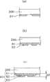
在图6(f)中,标志符号80的第1层81是10μm左右,但第2层82是15μm左右或者以上。由此,标志符号80的第2层82部分的厚度d2成为25μm以上。便携电话等中使用的液晶显示装置由于要求薄型,所以如果标志符号80的厚度变大,则有时会产生问题。In FIG. 6( f ), the
图7是图4所示的液晶显示装置的标志符号80附近处的详细剖面图。在图7中,粘接材料片210的厚度d1是例如100μm。标志符号80的2层部中的厚度d2是例如25μm。触摸面板用柔性布线基板50的厚度是70μm左右。在图7中,粘接材料片210的厚度d1勉强大于标志符号80的厚度d2与触摸面板用柔性布线基板50的厚度d3的合计。FIG. 7 is a detailed cross-sectional view of the vicinity of
但是,如果考虑部件的厚度的偏差,则还有时d1小于d2与d3的合计、即d1<d2+d3。另外,由于总是对液晶显示装置提出薄型化的要求,所以还预想进一步减小粘接材料片210的厚度的情况。由此,还假设使d1<d2+d3成为常态的情况。However, considering the variation in the thickness of the member, d1 may be smaller than the sum of d2 and d3, that is, d1<d2+d3. In addition, since liquid crystal display devices are always required to be thinner, it is expected that the thickness of the
在d1<d2+d3的情况下,如果标志符号80配置在与前窗200、触摸面板用柔性布线基板50、触摸面板100的重叠的部分,则产生剥离通过粘接材料片210粘接的前窗200与触摸面板100的应力。另外,在图7中,标志符号80的第1层81进入到粘接材料片210之下,但在该部分中粘接材料片210被压扁而厚度变小。因此,在对厚度进行比较的情况下,对粘接材料片210的厚度d1与其他厚度进行比较即可。In the case of d1<d2+d3, if the
在本发明中,虽然使标志符号80的位置与触摸面板用柔性布线基板50重叠,但通过配置在不与触摸面板100重叠的位置,而防止产生剥离前窗200与触摸面板100的应力。即,在图7中,将标志符号80的第2层82的端部与触摸面板100的端部的距离L设为0以上。In the present invention,
通过设为这样的结构,即使假设标志符号80与触摸面板用柔性布线基板50的厚度的合计大于粘接材料片210的厚度,由于触摸面板用柔性布线基板50能够向下侧移动,所以不会对粘接材料片210施加剥离应力。因此,可以实现可靠性高的液晶显示装置。With such a configuration, even if the sum of the thickness of the
实施例2Example 2
如果对形成在前窗200的背面的标志符号80入射了来自背光源的发光二极管的光,则有时无法在标志符号80的颜色等中得到规定的设计性。为了防止该现象,在实施例1中,通过加厚标志符号80的第2层82来解决。但是,在实施例1中有时得不到充分的遮光效果。在本实施例中,通过在用于对标志符号80形成白色或规定颜色的第2层82上进一步形成作为遮光膜的第3层83,防止来自发光二极管的光的影响。If the light from the light emitting diodes of the backlight is incident on the
图8是示出形成本实施例中的标志符号80的工艺的剖面图。图8(a)是将第1层81形成在前窗200的背面的图,图8(b)是形成了第2层82的图,图8(c)是形成了第3层83的图。第1层81的厚度是10μm左右,第2层82的厚度是10μm左右,第3层83的厚度也是10μm左右。FIG. 8 is a cross-sectional view showing a process of forming a
在本实施例中,与实施例1的情况相比,第2层82的厚度减小了形成了作为遮光膜的第3层83的量。第2层82由树脂形成,分散有白色或者规定颜色的颜料。作为遮光膜的第3层83是黑色的,是在环氧树脂等有机树脂中分散了黑色的颜料。In this example, compared with the case of example 1, the thickness of the
为了完全遮光,第3层83还覆盖第2层82的侧部。在图8(c)中,从第1层81到第3层83的厚度的合计d2是例如30μm左右。在粘接材料片210的厚度、以及触摸面板用柔性布线基板50的厚度的关系中,图8(c)中的标志符号80的厚度d2成为问题。The
图9是成为3层的标志符号80形成在前窗200的背面的情况的剖面图。在图9中,粘接材料片210的厚度d1是100μm,触摸面板用柔性布线基板50的厚度d3是70μm,标志符号80的3层部分的厚度d2是30μm。如果考虑部件的制造公差,则半数成为d1<d2+d3。FIG. 9 is a cross-sectional view of a case where three layers of
在图9中,标志符号80的第3层83的端部形成在触摸面板100的端部的外侧。即,图9的L大于零。因此,即使成为d1<d2+d3的关系,触摸面板用柔性布线基板50也可以向下侧移动,所以不会产生前窗200与触摸面板100之间的粘接材料片210的剥离应力。In FIG. 9 , the end of the
图9的L是在俯视观察的情况的第2层82的端部与触摸面板100的端部的距离。换言之,在标志符号80中,成为3层结构的部分的端部与触摸面板100的端部的距离是L。L in FIG. 9 is the distance between the end of the
这样,即使以3层形成了标志符号80,根据本实施例的结构,也不会产生前窗200与触摸面板用柔性布线基板50的剥离应力。因此,可以防止液晶显示装置的可靠性降低。In this way, even if the
实施例3Example 3
在实施例1中,使标志符号80的第2层82与触摸面板100的端部的距离L大于零,在实施例2中,使标志符号80的成为3层结构的部分的端部与触摸面板100的端部的距离L大于零。在距离L接近零的附近处,弯曲应力较大,所以在图7等中,在d1<d2+d3的情况下,有时存在针对前窗200与触摸面板用柔性布线基板50之间的粘接材料片210的剥离应力。In Embodiment 1, the distance L between the
本实施例解决了该问题。图10是本实施例中的前窗200的背面形成的标志符号80附近的详细剖面图。在图10中,省略了触摸面板100以下的结构。This embodiment solves this problem. FIG. 10 is a detailed cross-sectional view of the vicinity of the
在图10中,在触摸面板100中安装了触摸面板用柔性布线基板50。触摸面板用柔性布线基板50成为在基材52上形成有铜布线53、且表皮54膜覆盖了铜布线53的结构。在触摸面板用柔性布线基板50与触摸面板100连接的部分不存在表皮5,而形成有Ni层55、Au层56。In FIG. 10 , a touch panel
图10中的各部件的厚度例如如下所述。触摸面板用柔性布线基板50的基材52的厚度是40μm,铜布线53的厚度是20μm,表皮54的厚度是25μm,端子部中的Ni层55的厚度是1μm至5μm,Au层56的厚度是0.03~0.3μm。在形成有表皮54的部分不存在Ni层55以及Au层56。在图10中,将触摸面板用柔性布线基板50与粘接材料片210的厚度d1、标志符号80的厚度d2进行比较时的厚度为没有表皮54的部分的厚度d3。The thickness of each member in FIG. 10 is as follows, for example. The thickness of the
图10中的标志符号80的厚度与实施例1的情况相同,第1层81是10μm,第2层82是15μm。另外,粘接材料片210的厚度d1是100μm。但是,这些部件的厚度存在偏差的情况较多。在图10中,通过将L设为0.3mm以上,即使产生了d1<d2+d3的关系,由于将L的值设为0.3以上,所以可以极力减小施加到粘接材料片210的剥离应力。The thicknesses of
在图10中,在触摸面板用柔性布线基板50的表皮54的端部与触摸面板100的端部的距离M极端小的情况下,触摸面板用柔性布线基板50的弯曲应力变大。但是,在本实施例中,由于标志符号80的第2层82的端部与触摸面板100的端部的距离L是0.3mm以上,所以可以将触摸面板用柔性布线基板50的弯曲应力抑制得较小,可以抑制由于弯曲应力引起的粘接材料片210的剥离应力。In FIG. 10 , when the distance M between the end of the
在图10中,说明了标志符号80是2层的情况,但即使在标志符号80如实施例2那样由3层形成的情况也相同。In FIG. 10 , the case where the
Claims (5)
Translated fromChineseApplications Claiming Priority (2)
| Application Number | Priority Date | Filing Date | Title |
|---|---|---|---|
| JP2009-107678 | 2009-04-27 | ||
| JP2009107678AJP5235769B2 (en) | 2009-04-27 | 2009-04-27 | Liquid crystal display |
Publications (2)
| Publication Number | Publication Date |
|---|---|
| CN101872084Atrue CN101872084A (en) | 2010-10-27 |
| CN101872084B CN101872084B (en) | 2012-09-12 |
Family
ID=42321096
Family Applications (1)
| Application Number | Title | Priority Date | Filing Date |
|---|---|---|---|
| CN2010101661380AActiveCN101872084B (en) | 2009-04-27 | 2010-04-23 | Liquid crystal display device |
Country Status (6)
| Country | Link |
|---|---|
| US (6) | US8581862B2 (en) |
| EP (1) | EP2246730B1 (en) |
| JP (1) | JP5235769B2 (en) |
| KR (1) | KR101212345B1 (en) |
| CN (1) | CN101872084B (en) |
| TW (1) | TWI490592B (en) |
Cited By (7)
| Publication number | Priority date | Publication date | Assignee | Title |
|---|---|---|---|---|
| CN102955598A (en)* | 2011-08-25 | 2013-03-06 | 联胜(中国)科技有限公司 | Touch panel and touch display device |
| CN102968203A (en)* | 2011-09-01 | 2013-03-13 | 阿尔卑斯电气株式会社 | Input device and method for manufacturing the same |
| CN103782257A (en)* | 2011-09-06 | 2014-05-07 | 凸版印刷株式会社 | Integrated touch sensor substrate, display device provided with same, and method for producing integrated touch sensor substrate |
| CN105976701A (en)* | 2015-03-10 | 2016-09-28 | 三星显示有限公司 | Display device and portable terminal |
| CN110441950A (en)* | 2019-06-11 | 2019-11-12 | 惠科股份有限公司 | Display panel and display device |
| CN111989730A (en)* | 2018-02-26 | 2020-11-24 | 株式会社大阪看板 | Display device with three-dimensional logo |
| CN113641047A (en)* | 2021-08-10 | 2021-11-12 | 豪威半导体(上海)有限责任公司 | Flexible board packaging structure and LCOS device |
Families Citing this family (41)
| Publication number | Priority date | Publication date | Assignee | Title |
|---|---|---|---|---|
| JP5235769B2 (en)* | 2009-04-27 | 2013-07-10 | 株式会社ジャパンディスプレイイースト | Liquid crystal display |
| US20130018489A1 (en)* | 2011-07-14 | 2013-01-17 | Grunthaner Martin Paul | Combined force and proximity sensing |
| CN102999200A (en)* | 2011-09-18 | 2013-03-27 | 宸鸿科技(厦门)有限公司 | Touch display device and manufacturing method thereof |
| KR101357592B1 (en)* | 2011-09-28 | 2014-02-04 | 엘지이노텍 주식회사 | Touch-Window |
| FR2985076B1 (en)* | 2011-12-23 | 2014-08-29 | Valeo Systemes Thermiques | CONTROL AND DISPLAY MODULE FOR A MOTOR VEHICLE AND METHOD FOR MANUFACTURING THE SAME |
| CN103176641A (en)* | 2011-12-25 | 2013-06-26 | 宸鸿科技(厦门)有限公司 | Touch panel and manufacturing method thereof |
| JP6086278B2 (en)* | 2012-02-20 | 2017-03-01 | 大日本印刷株式会社 | Front protective plate for display device with wiring, manufacturing method thereof, and display device |
| JP6415798B2 (en)* | 2012-04-05 | 2018-10-31 | 大日本印刷株式会社 | Front protective plate for display device and display device |
| KR101976067B1 (en) | 2012-07-25 | 2019-05-09 | 삼성디스플레이 주식회사 | A display device providing touch emitting key unit |
| KR101946463B1 (en) | 2012-07-27 | 2019-02-12 | 삼성디스플레이 주식회사 | Laminating apparatus and laminating method |
| US20140098332A1 (en)* | 2012-10-10 | 2014-04-10 | Apple Inc. | Displays With Logos and Alignment Marks |
| KR102035005B1 (en)* | 2012-12-24 | 2019-10-22 | 엘지디스플레이 주식회사 | Touch display device |
| CN104123022B (en)* | 2013-04-24 | 2017-07-28 | 宸鸿科技(厦门)有限公司 | Contact panel and its covering plate structure |
| US20140353020A1 (en)* | 2013-05-30 | 2014-12-04 | Tianjin Funayuanchuang Technology Co., Ltd. | Touch panel |
| KR101490172B1 (en)* | 2013-06-05 | 2015-02-05 | 주식회사 라온이노텍 | Transparent member having an image and method for forming the image on the transparent member |
| TWI562030B (en)* | 2013-07-02 | 2016-12-11 | Touch panel structure, method for forming touch panel structure and touch device thereof | |
| TWI515617B (en)* | 2013-08-07 | 2016-01-01 | 達鴻先進科技股份有限公司 | Touch panel structure and method for forming the same |
| JP2015041021A (en)* | 2013-08-23 | 2015-03-02 | 大日本印刷株式会社 | Front protective plate for display device and display device |
| KR102107564B1 (en) | 2013-11-06 | 2020-05-08 | 삼성디스플레이 주식회사 | Liquid crystal device |
| US9638950B2 (en)* | 2014-05-15 | 2017-05-02 | Apple Inc. | Display with opaque border resistant to electrostatic discharge |
| JP2016099463A (en)* | 2014-11-20 | 2016-05-30 | 株式会社ジャパンディスプレイ | Liquid crystal display device |
| JP6455154B2 (en)* | 2015-01-08 | 2019-01-23 | 株式会社デンソー | Vehicle electronics |
| JP6448391B2 (en)* | 2015-01-28 | 2019-01-09 | 株式会社ジャパンディスプレイ | Display module |
| KR102379745B1 (en)* | 2015-07-06 | 2022-03-29 | 삼성디스플레이 주식회사 | Display apparatus |
| KR102500048B1 (en) | 2015-11-20 | 2023-02-16 | 삼성디스플레이 주식회사 | Window substrate and display apparatus including the same |
| KR102495325B1 (en) | 2016-01-11 | 2023-02-03 | 삼성디스플레이 주식회사 | Window member and manufacturing method of the same |
| TWI584105B (en)* | 2016-01-11 | 2017-05-21 | Memory module and manufacturing method thereof | |
| JP6411389B2 (en)* | 2016-02-04 | 2018-10-24 | 大日本印刷株式会社 | Front protective plate for display device and display device |
| CN106020554A (en)* | 2016-06-06 | 2016-10-12 | 京东方科技集团股份有限公司 | Tough cover plate, manufacturing method thereof and touch display device |
| WO2018057652A1 (en)* | 2016-09-22 | 2018-03-29 | Apple Inc. | Display module & glass with undercut plastic frame |
| CN111316209A (en)* | 2017-08-30 | 2020-06-19 | 深圳传音通讯有限公司 | Terminal processing method, terminal processing device and computer-readable storage medium |
| JP2019045767A (en)* | 2017-09-05 | 2019-03-22 | 株式会社ジャパンディスプレイ | Display |
| KR101948556B1 (en)* | 2017-09-06 | 2019-02-18 | (주)코텍 | Image display device of slot machine apparatus |
| KR102433103B1 (en) | 2017-10-02 | 2022-08-17 | 삼성디스플레이 주식회사 | Display device |
| US10939544B2 (en)* | 2018-05-10 | 2021-03-02 | Dura Operating, Llc | Multiple resin over-mold for printed circuit board electronics and light guide |
| KR102715075B1 (en)* | 2018-10-12 | 2024-10-10 | 삼성디스플레이 주식회사 | Display device |
| CN115362097A (en)* | 2020-04-15 | 2022-11-18 | 上海延锋金桥汽车饰件系统有限公司 | vehicle interior parts |
| US20230311804A1 (en)* | 2020-04-15 | 2023-10-05 | Shanghai Yanfeng Jinqiao Automotive Trim Systems Co. Ltd. | Component for vehicle interior |
| CN113808477A (en)* | 2020-06-15 | 2021-12-17 | 群创光电股份有限公司 | display device |
| US12176333B2 (en) | 2021-06-24 | 2024-12-24 | Hefei Boe Optoelectronics Technology Co., Ltd. | Backplane and method for manufacturing the same, backlight module, and display apparatus |
| WO2024118844A1 (en) | 2022-11-30 | 2024-06-06 | Yanfeng International Automotive Technology Co., Ltd. | Component for vehicle interior |
Citations (3)
| Publication number | Priority date | Publication date | Assignee | Title |
|---|---|---|---|---|
| WO2005059635A1 (en)* | 2003-12-19 | 2005-06-30 | Ekolite Co. Ltd. | Logo printing structure and printing method for lcd window |
| CN101042492A (en)* | 2006-03-24 | 2007-09-26 | 株式会社日立显示器 | Display device |
| JP2008083491A (en)* | 2006-09-28 | 2008-04-10 | Epson Imaging Devices Corp | Electro-optical device and electronic equipment |
Family Cites Families (15)
| Publication number | Priority date | Publication date | Assignee | Title |
|---|---|---|---|---|
| JPH05114329A (en)* | 1991-10-21 | 1993-05-07 | Nissha Printing Co Ltd | Transparent touch panel with display design |
| ATE174438T1 (en)* | 1994-10-04 | 1998-12-15 | Optrel Ag | ELECTRO-OPTICAL FILTER CASSETTE AND METHOD OF PRODUCTION THEREOF |
| JPH0934624A (en)* | 1995-07-17 | 1997-02-07 | Seiko Denshi Kiki Kk | Coordinate reader |
| EP1087286A4 (en)* | 1998-06-08 | 2007-10-17 | Kaneka Corp | Resistor film touch panel used for liquid crystal display and liquid crystal display with the same |
| US6358767B2 (en)* | 2000-06-08 | 2002-03-19 | Semiconductor Energy Laboratory Co., Ltd. | Method of manufacturing semiconductor device |
| US6462941B1 (en)* | 2000-06-30 | 2002-10-08 | Palm, Inc. | Method and apparatus for backlighting a handwriting input area for a portable computing device |
| DE10228523B4 (en)* | 2001-11-14 | 2017-09-21 | Lg Display Co., Ltd. | touch tablet |
| JP3891843B2 (en)* | 2002-01-08 | 2007-03-14 | 株式会社日立製作所 | Liquid crystal display |
| JP4215549B2 (en)* | 2003-04-02 | 2009-01-28 | 富士通株式会社 | Information processing device that operates in touch panel mode and pointing device mode |
| JP2005158008A (en)* | 2003-11-06 | 2005-06-16 | Matsushita Electric Ind Co Ltd | Touch panel and liquid crystal display device with touch panel using the same |
| JP4545424B2 (en)* | 2003-12-11 | 2010-09-15 | アルプス電気株式会社 | Coordinate input device and image display device and electronic apparatus provided with the same |
| JP2009069333A (en)* | 2007-09-12 | 2009-04-02 | Epson Imaging Devices Corp | Electro-optical apparatus and electronic apparatus |
| JP2009086077A (en)* | 2007-09-28 | 2009-04-23 | Hitachi Displays Ltd | Liquid crystal display device equipped with touch panel and manufacturing method thereof |
| CN101790712A (en)* | 2008-09-26 | 2010-07-28 | 讬福思株式会社 | Touch panel using tempered glass |
| JP5235769B2 (en)* | 2009-04-27 | 2013-07-10 | 株式会社ジャパンディスプレイイースト | Liquid crystal display |
- 2009
- 2009-04-27JPJP2009107678Apatent/JP5235769B2/enactiveActive
- 2010
- 2010-04-07TWTW099110744Apatent/TWI490592B/enactive
- 2010-04-20USUS12/763,450patent/US8581862B2/enactiveActive
- 2010-04-23CNCN2010101661380Apatent/CN101872084B/enactiveActive
- 2010-04-26KRKR1020100038666Apatent/KR101212345B1/ennot_activeExpired - Fee Related
- 2010-04-26EPEP10004406Apatent/EP2246730B1/enactiveActive
- 2013
- 2013-10-31USUS14/068,060patent/US9229561B2/enactiveActive
- 2015
- 2015-11-30USUS14/954,094patent/US9665195B2/ennot_activeExpired - Fee Related
- 2017
- 2017-04-21USUS15/493,239patent/US10088933B2/enactiveActive
- 2018
- 2018-08-28USUS16/114,392patent/US10678358B2/enactiveActive
- 2020
- 2020-05-01USUS16/864,222patent/US11150756B2/enactiveActive
Patent Citations (3)
| Publication number | Priority date | Publication date | Assignee | Title |
|---|---|---|---|---|
| WO2005059635A1 (en)* | 2003-12-19 | 2005-06-30 | Ekolite Co. Ltd. | Logo printing structure and printing method for lcd window |
| CN101042492A (en)* | 2006-03-24 | 2007-09-26 | 株式会社日立显示器 | Display device |
| JP2008083491A (en)* | 2006-09-28 | 2008-04-10 | Epson Imaging Devices Corp | Electro-optical device and electronic equipment |
Cited By (13)
| Publication number | Priority date | Publication date | Assignee | Title |
|---|---|---|---|---|
| CN102955598A (en)* | 2011-08-25 | 2013-03-06 | 联胜(中国)科技有限公司 | Touch panel and touch display device |
| CN102968203A (en)* | 2011-09-01 | 2013-03-13 | 阿尔卑斯电气株式会社 | Input device and method for manufacturing the same |
| CN102968203B (en)* | 2011-09-01 | 2015-12-02 | 阿尔卑斯电气株式会社 | Input media and manufacture method thereof |
| CN103782257A (en)* | 2011-09-06 | 2014-05-07 | 凸版印刷株式会社 | Integrated touch sensor substrate, display device provided with same, and method for producing integrated touch sensor substrate |
| US10540032B2 (en) | 2015-03-10 | 2020-01-21 | Samsung Display Co., Ltd. | Display device having durable circuit board |
| CN105976701A (en)* | 2015-03-10 | 2016-09-28 | 三星显示有限公司 | Display device and portable terminal |
| CN111276049A (en)* | 2015-03-10 | 2020-06-12 | 三星显示有限公司 | Display devices and portable terminals |
| CN111276049B (en)* | 2015-03-10 | 2022-02-08 | 三星显示有限公司 | Display device and portable terminal |
| US11455049B2 (en) | 2015-03-10 | 2022-09-27 | Samsung Display Co., Ltd. | Display device with compensating film |
| CN111989730A (en)* | 2018-02-26 | 2020-11-24 | 株式会社大阪看板 | Display device with three-dimensional logo |
| CN110441950A (en)* | 2019-06-11 | 2019-11-12 | 惠科股份有限公司 | Display panel and display device |
| CN113641047A (en)* | 2021-08-10 | 2021-11-12 | 豪威半导体(上海)有限责任公司 | Flexible board packaging structure and LCOS device |
| CN113641047B (en)* | 2021-08-10 | 2023-08-25 | 豪威半导体(上海)有限责任公司 | Soft board packaging structure and LCOS device |
Also Published As
| Publication number | Publication date |
|---|---|
| JP5235769B2 (en) | 2013-07-10 |
| JP2010256682A (en) | 2010-11-11 |
| US10088933B2 (en) | 2018-10-02 |
| US10678358B2 (en) | 2020-06-09 |
| EP2246730A2 (en) | 2010-11-03 |
| US20170220167A1 (en) | 2017-08-03 |
| TWI490592B (en) | 2015-07-01 |
| CN101872084B (en) | 2012-09-12 |
| US20100271329A1 (en) | 2010-10-28 |
| US9229561B2 (en) | 2016-01-05 |
| US20200257398A1 (en) | 2020-08-13 |
| US11150756B2 (en) | 2021-10-19 |
| EP2246730A3 (en) | 2011-06-15 |
| KR101212345B1 (en) | 2012-12-13 |
| US20180364848A1 (en) | 2018-12-20 |
| US8581862B2 (en) | 2013-11-12 |
| EP2246730B1 (en) | 2013-01-23 |
| TW201107824A (en) | 2011-03-01 |
| US9665195B2 (en) | 2017-05-30 |
| US20160085349A1 (en) | 2016-03-24 |
| US20140055691A1 (en) | 2014-02-27 |
| KR20100118081A (en) | 2010-11-04 |
Similar Documents
| Publication | Publication Date | Title |
|---|---|---|
| CN101872084B (en) | Liquid crystal display device | |
| US9436340B2 (en) | Liquid crystal display device with touch panel | |
| JP4321537B2 (en) | Liquid crystal device and method for manufacturing liquid crystal device | |
| JP5308749B2 (en) | Liquid crystal display | |
| TWI416200B (en) | Liquid crystal display device | |
| US8379163B2 (en) | Display device | |
| CN101382675B (en) | Electro optical device and electronic apparatus | |
| US9766654B2 (en) | Liquid crystal display device | |
| JP2012137607A (en) | Display device, manufacturing method thereof and electronic apparatus | |
| JP2012145779A (en) | Liquid crystal display device | |
| JP5385475B2 (en) | Mobile phone equipment | |
| JP5714678B2 (en) | Mobile phone equipment | |
| CN113823185B (en) | electronic device |
Legal Events
| Date | Code | Title | Description |
|---|---|---|---|
| C06 | Publication | ||
| PB01 | Publication | ||
| C10 | Entry into substantive examination | ||
| SE01 | Entry into force of request for substantive examination | ||
| ASS | Succession or assignment of patent right | Owner name:PANASONIC LCD CO., LTD. Free format text:FORMER OWNER: IPS ALPHA SUPPORT CO., LTD. Effective date:20111129 Owner name:IPS ALPHA SUPPORT CO., LTD. Effective date:20111129 | |
| C41 | Transfer of patent application or patent right or utility model | ||
| TA01 | Transfer of patent application right | Effective date of registration:20111129 Address after:Chiba County, Japan Applicant after:Hitachi Displays, Ltd. Co-applicant after:Panasonic Liquid Crystal Display Co.,Ltd. Address before:Chiba County, Japan Applicant before:Hitachi Displays, Ltd. Co-applicant before:IPS pioneer support society Effective date of registration:20111129 Address after:Chiba County, Japan Applicant after:Hitachi Displays, Ltd. Co-applicant after:IPS Pioneer Support Society Address before:Chiba County, Japan Applicant before:Hitachi Displays, Ltd. | |
| C14 | Grant of patent or utility model | ||
| GR01 | Patent grant | ||
| C56 | Change in the name or address of the patentee | Owner name:APAN DISPLAY EAST, INC. Free format text:FORMER NAME: HITACHI DISPLAY CO., LTD. Owner name:JAPAN DISPLAY, INC. Free format text:FORMER NAME: APAN DISPLAY EAST, INC. | |
| CP01 | Change in the name or title of a patent holder | Address after:Chiba County, Japan Patentee after:JAPAN DISPLAY Inc. Patentee after:Panasonic Liquid Crystal Display Co.,Ltd. Address before:Chiba County, Japan Patentee before:Japan Display East Inc. Patentee before:Panasonic Liquid Crystal Display Co.,Ltd. Address after:Chiba County, Japan Patentee after:Japan Display East Inc. Patentee after:Panasonic Liquid Crystal Display Co.,Ltd. Address before:Chiba County, Japan Patentee before:Hitachi Displays, Ltd. Patentee before:Panasonic Liquid Crystal Display Co.,Ltd. | |
| CP02 | Change in the address of a patent holder | Address after:Tokyo, Japan Patentee after:JAPAN DISPLAY Inc. Patentee after:Panasonic Liquid Crystal Display Co.,Ltd. Address before:Chiba County, Japan Patentee before:JAPAN DISPLAY Inc. Patentee before:Panasonic Liquid Crystal Display Co.,Ltd. | |
| EE01 | Entry into force of recordation of patent licensing contract | Application publication date:20101027 Assignee:BOE TECHNOLOGY GROUP Co.,Ltd. Assignor:JAPAN DISPLAY Inc.|Panasonic Liquid Crystal Display Co.,Ltd. Contract record no.:2013990000688 Denomination of invention:Liquid crystal display device Granted publication date:20120912 License type:Common License Record date:20131016 | |
| LICC | Enforcement, change and cancellation of record of contracts on the licence for exploitation of a patent or utility model | ||
| TR01 | Transfer of patent right | ||
| TR01 | Transfer of patent right | Effective date of registration:20231012 Address after:Tokyo Patentee after:JAPAN DISPLAY Inc. Patentee after:PANASONIC INTELLECTUAL PROPERTY CORPORATION OF AMERICA Address before:Tokyo Patentee before:JAPAN DISPLAY Inc. Patentee before:Panasonic Liquid Crystal Display Co.,Ltd. | |
| TR01 | Transfer of patent right | Effective date of registration:20240911 Address after:6600 Chase Oaks Avenue, Unit 150, Plano, Texas 75023, United States Patentee after:Touch Panel Technology Co.,Ltd. Country or region after:U.S.A. Address before:Tokyo, Japan Patentee before:JAPAN DISPLAY Inc. Country or region before:Japan Patentee before:PANASONIC INTELLECTUAL PROPERTY CORPORATION OF AMERICA Country or region before:U.S.A. | |
| TR01 | Transfer of patent right |