CN101868116B - Circuit board and manufacturing method thereof - Google Patents
Circuit board and manufacturing method thereofDownload PDFInfo
- Publication number
- CN101868116B CN101868116BCN2009101344852ACN200910134485ACN101868116BCN 101868116 BCN101868116 BCN 101868116BCN 2009101344852 ACN2009101344852 ACN 2009101344852ACN 200910134485 ACN200910134485 ACN 200910134485ACN 101868116 BCN101868116 BCN 101868116B
- Authority
- CN
- China
- Prior art keywords
- blocking structure
- laser blocking
- dielectric layer
- layer
- circuit board
- Prior art date
- Legal status (The legal status is an assumption and is not a legal conclusion. Google has not performed a legal analysis and makes no representation as to the accuracy of the status listed.)
- Active
Links
- 238000004519manufacturing processMethods0.000titleclaimsabstractdescription27
- 230000000903blocking effectEffects0.000claimsabstractdescription125
- 239000000758substrateSubstances0.000claimsdescription26
- 238000000034methodMethods0.000claimsdescription18
- 238000003754machiningMethods0.000claimsdescription4
- 238000005530etchingMethods0.000claimsdescription2
- 239000010410layerSubstances0.000description131
- 238000012545processingMethods0.000description16
- 230000000694effectsEffects0.000description4
- 230000007547defectEffects0.000description3
- 238000012986modificationMethods0.000description3
- 230000004048modificationEffects0.000description3
- 239000011241protective layerSubstances0.000description2
- 230000009286beneficial effectEffects0.000description1
- 238000013461designMethods0.000description1
- 238000012827research and developmentMethods0.000description1
Images


Landscapes
- Laser Beam Processing (AREA)
Abstract
Description
Translated fromChinese技术领域technical field
本发明涉及一种线路板及其制作方法,特别是涉及一种可有效控制激光加工深度的线路板及其制作方法。 The invention relates to a circuit board and a manufacturing method thereof, in particular to a circuit board capable of effectively controlling the depth of laser processing and a manufacturing method thereof. the
背景技术Background technique
随着市场对于电子产品具有轻薄短小且携带方便的需求,因此电子产品中的电子零件亦需随之朝向小型化与薄型化的方向发展。为此,现有习知技术提出一种局部降低线路板厚度的方法。 As the market demands for electronic products that are thin, light, small and portable, the electronic components in the electronic products also need to be developed in the direction of miniaturization and thinning. For this reason, the prior art proposes a method for partially reducing the thickness of the circuit board. the
图1A~图1C为现有习知的线路板的制造工艺剖面图。图2为图1A~图1C中的线路基板的俯视图,其中图1A~图1C为现有习知的线路板制造工艺沿图2中的剖面线I-I’的剖面图。 1A-1C are cross-sectional views of a conventional circuit board manufacturing process. 2 is a top view of the circuit substrate in FIGS. 1A to 1C , wherein FIGS. 1A to 1C are cross-sectional views along the section line I-I' in FIG. 2 of a conventional circuit board manufacturing process. the
首先,请同时参阅图1A与图2所示,提供一线路基板100,其具有一第一介电层110、一第二介电层120、一线路层130、一第三介电层140以及一第四介电层150。第二介电层120、第三介电层140以及第四介电层150依序堆叠于第一介电层110上,且线路层130配置于第二介电层120上并位于第二与第三介电层120、140之间。线路基板100具有一预移除区L。 First, please refer to FIG. 1A and FIG. 2 at the same time, a
接着,请参阅图1B所示,以激光加工的方式移除第三介电层140以及第四介电层150的位于预移除区L周边的部分。然后,请参阅图1C所示,移除第三介电层140以及第四介电层150之位于预移除区L内的部分,以形成一移除区L1,此时,已大致形成一线路板P。由于线路板P的移除区L1的厚度小于线路板P的其他区域的厚度,因此,在实际应用上,电子元件200可配置于移除区L1内,如此,可降低线路板P与配置于其上的电子元件200的总厚度。 Next, as shown in FIG. 1B , parts of the third
然而,以激光加工的方式移除第三介电层140以及第四介电层150时,不易控制激光加工的深度。因此,容易过度烧蚀(over trench)第二介电层120甚至是第一介电层110。 However, when the third
由此可见,上述现有的线路板及其制作方法在产品结构、制造方法与使用上,显然仍存在有不便与缺陷,而亟待加以进一步改进。为了解决上述存在的问题,相关厂商莫不费尽心思来谋求解决之道,但长久以来一直未见适用的设计被发展完成,而一般产品及方法又没有适切的结构及方法能够解决上述问题,此显然是相关业者急欲解决的问题。因此如何能创设一种新的线路板及其制作方法,实属当前重要研发课题之一,亦成为当前业界极需改进的目标。It can be seen that the above-mentioned existing circuit board and its manufacturing method obviously still have inconvenience and defects in terms of product structure, manufacturing method and use, and need to be further improved urgently. In order to solve the above-mentioned problems, the relevant manufacturers have tried their best to find a solution, but no suitable design has been developed for a long time, and there is no suitable structure and method for general products and methods to solve the above-mentioned problems. This is obviously a problem that relevant industry players are eager to solve. Therefore, how to create a new circuit board and its manufacturing method is one of the current important research and development topics, and has also become a goal that the industry needs to improve.
发明内容Contents of the invention
本发明的目的在于,克服现有的线路板存在的缺陷,而提供一种新的线路板,所要解决的技术问题是使其具有可有效控制激光加工深度的线路板结构,非常适于实用。 The purpose of the present invention is to overcome the defects of the existing circuit board and provide a new circuit board. The technical problem to be solved is to make it have a circuit board structure that can effectively control the depth of laser processing, which is very suitable for practical use. the
本发明的另一目的在于,克服现有的线路板的制作方法存在的缺陷,而提供一种新的线路板的制作方法,所要解决的技术问题是使其可有效控制激光加工深度,从而更加适于实用。 Another object of the present invention is to overcome the defects of the existing circuit board manufacturing method and provide a new circuit board manufacturing method. The technical problem to be solved is to make it possible to effectively control the laser processing depth, thereby more Suitable for practical use. the
本发明的目的及解决其技术问题是采用以下技术方案来实现的。依据本发明提出的一种线路板,其具有一移除区。线路板包括一第一介电层、一第一激光阻挡结构、一第二介电层、一线路层、一第二激光阻挡结构以及一第三介电层。第一激光阻挡结构配置于第一介电层的一第一表面,且位于移除区的边缘上。第二介电层配置于第一介电层上,并覆盖第一激光阻挡结构。线路层配置于第二介电层的一第二表面上,且部分线路层由移除区外延伸进移除区内。第二激光阻挡结构配置于第二表面上并位于移除区的边缘上,且与线路层绝缘,第二激光阻挡结构与线路层之间存在至少一间隙,间隙在第一表面上的垂直投影与第一激光阻挡结构重叠。第三介电层配置于第二介电层上,并具有对应移除区的一开口,开口暴露出线路层的位于移除区内的部分以及第二激光阻挡结构的位于移除区内的部分。 The purpose of the present invention and the solution to its technical problems are achieved by adopting the following technical solutions. According to a circuit board provided by the present invention, it has a removal area. The circuit board includes a first dielectric layer, a first laser blocking structure, a second dielectric layer, a circuit layer, a second laser blocking structure and a third dielectric layer. The first laser blocking structure is configured on a first surface of the first dielectric layer and is located on the edge of the removal area. The second dielectric layer is disposed on the first dielectric layer and covers the first laser blocking structure. The wiring layer is disposed on a second surface of the second dielectric layer, and part of the wiring layer extends from outside the removal area into the removal area. The second laser blocking structure is arranged on the second surface and is located on the edge of the removal area, and is insulated from the circuit layer. There is at least one gap between the second laser blocking structure and the circuit layer. The vertical projection of the gap on the first surface Overlapping with the first laser blocking structure. The third dielectric layer is disposed on the second dielectric layer and has an opening corresponding to the removal area, and the opening exposes a part of the circuit layer located in the removal area and a portion of the second laser blocking structure located in the removal area. part. the
本发明的目的及解决其技术问题还可采用以下技术措施进一步实现。 The purpose of the present invention and its technical problems can also be further realized by adopting the following technical measures. the
在本发明的一实施例中,第二激光阻挡结构为一环状结构,环状结构具有至少一缺口,且线路层由缺口延伸进移除区内。 In an embodiment of the present invention, the second laser blocking structure is a ring structure, the ring structure has at least one gap, and the circuit layer extends into the removal area from the gap. the
在本发明的一实施例中,当第二激光阻挡结构与线路层之间存在多个间隙时,第一激光阻挡结构包括多个彼此独立的点状结构。 In an embodiment of the present invention, when there are multiple gaps between the second laser blocking structure and the circuit layer, the first laser blocking structure includes multiple independent dot structures. the
在本发明的一实施例中,第一激光阻挡结构包括一条状结构。 In an embodiment of the invention, the first laser blocking structure includes a strip structure. the
在本发明的一实施例中,条状结构与第二激光阻挡结构在第一表面上的垂直投影重叠。 In an embodiment of the present invention, the strip structure overlaps with the vertical projection of the second laser blocking structure on the first surface. the
在本发明的一实施例中,第二介电层具有至少一凹槽(cavity),且凹槽位于间隙下方。 In an embodiment of the invention, the second dielectric layer has at least one cavity, and the cavity is located below the gap. the
在本发明的一实施例中,凹槽暴露出第一激光阻挡结构。 In an embodiment of the invention, the groove exposes the first laser blocking structure. the
在本发明的一实施例中,线路板更包括一第三激光阻挡结构,第三激光阻挡结构配置于第二表面上并位于移除区的边缘上,第三激光阻挡结构与线路层的位于移除区边缘的部分相连,并与第二激光阻挡结构绝缘。 In an embodiment of the present invention, the circuit board further includes a third laser blocking structure, the third laser blocking structure is disposed on the second surface and is located on the edge of the removal area, the third laser blocking structure and the wiring layer are located A portion of the edge of the removed region is connected to and insulated from the second laser blocking structure. the
在本发明的一实施例中,线路板更包括一保护层,保护层覆盖线路层的位于移除区内的部分。 In an embodiment of the present invention, the circuit board further includes a protection layer, and the protection layer covers a portion of the circuit layer located in the removal area. the
本发明的目的及解决其技术问题是采用以下技术方案来实现的。依据本发明提出的一种线路板的制作方法如下所述。首先,提供一基板,基板具有一预移除区。基板包括一第一介电层、一第一激光阻挡结构、一第二介电层、一线路层、一第二激光阻挡结构以及一第三介电层。第一激光阻挡结构配置于第一介电层的一第一表面,且位于预移除区的边缘上。第二介电层配置于第一介电层上,并覆盖第一激光阻挡结构。线路层配置于第二介电层的一第二表面上,且部分线路层由预移除区外延伸进预移除区内。第二激光阻挡结构配置于第二表面上并位于预移除区的边缘上,且与线路层绝缘,第二激光阻挡结构与线路层之间存在至少一间隙,且间隙在第一表面上的垂直投影与第一激光阻挡结构重叠。第三介电层配置于第二介电层上,并覆盖线路层与第二激光阻挡结构。接着,进行一激光加工制造工艺,以蚀刻位于预移除区的边缘上的第三介电层。然后,移除第三介电层之位于预移除区内的部分。 The purpose of the present invention and the solution to its technical problems are achieved by adopting the following technical solutions. A method for manufacturing a circuit board according to the present invention is as follows. Firstly, a substrate is provided, and the substrate has a pre-removal area. The substrate includes a first dielectric layer, a first laser blocking structure, a second dielectric layer, a circuit layer, a second laser blocking structure and a third dielectric layer. The first laser blocking structure is disposed on a first surface of the first dielectric layer and is located on the edge of the pre-removal area. The second dielectric layer is disposed on the first dielectric layer and covers the first laser blocking structure. The wiring layer is disposed on a second surface of the second dielectric layer, and part of the wiring layer extends from the pre-removal area into the pre-removal area. The second laser blocking structure is arranged on the second surface and is located on the edge of the pre-removal area, and is insulated from the circuit layer. There is at least one gap between the second laser blocking structure and the circuit layer, and the gap is on the first surface. The vertical projection overlaps with the first laser blocking structure. The third dielectric layer is disposed on the second dielectric layer and covers the circuit layer and the second laser blocking structure. Next, a laser machining process is performed to etch the third dielectric layer on the edge of the pre-removal area. Then, the part of the third dielectric layer located in the pre-removal area is removed. the
本发明的目的及解决其技术问题还可采用以下技术措施进一步实现。 The purpose of the present invention and its technical problems can also be further realized by adopting the following technical measures. the
在本发明的一实施例中,激光加工制造工艺更包括蚀刻第二介电层的位于间隙下的部分。 In an embodiment of the invention, the laser machining process further includes etching a portion of the second dielectric layer under the gap. the
在本发明的一实施例中,移除第三介电层的方法包括剥除法。 In an embodiment of the invention, the method for removing the third dielectric layer includes a stripping method. the
在本发明的一实施例中,第二激光阻挡结构为一环状结构,环状结构具有至少一缺口,且线路层由缺口延伸进预移除区内。 In an embodiment of the present invention, the second laser blocking structure is a ring structure, the ring structure has at least one gap, and the circuit layer extends into the pre-removal area from the gap. the
在本发明的一实施例中,当第二激光阻挡结构与线路层之间存在多个间隙时,第一激光阻挡结构包括多个彼此独立的点状结构。 In an embodiment of the present invention, when there are multiple gaps between the second laser blocking structure and the circuit layer, the first laser blocking structure includes multiple independent dot structures. the
在本发明的一实施例中,第一激光阻挡结构包括一条状结构或一环状结构。 In an embodiment of the invention, the first laser blocking structure includes a strip structure or a ring structure. the
在本发明的一实施例中,基板更包括一第三激光阻挡结构,第三激光阻挡结构配置于第二表面上并位于预移除区的边缘上,第三激光阻挡结构与线路层的位于移除区边缘的部分相连,并与第二激光阻挡结构绝缘。 In an embodiment of the present invention, the substrate further includes a third laser blocking structure, the third laser blocking structure is disposed on the second surface and is located on the edge of the pre-removed area, the third laser blocking structure and the circuit layer are located A portion of the edge of the removed region is connected to and insulated from the second laser blocking structure. the
在本发明的一实施例中,基板更包括一保护层,保护层覆盖线路层的位于预移除区内的部分。 In an embodiment of the present invention, the substrate further includes a protection layer, and the protection layer covers a portion of the circuit layer located in the pre-removal area. the
借由上述技术方案,本发明线路板及其制作方法至少具有下列优点及有益效果: By virtue of the above technical solutions, the circuit board of the present invention and its manufacturing method have at least the following advantages and beneficial effects:
由于本发明的线路板具有第一与第二激光阻挡结构,故本发明可利用第二激光阻挡结构来控制激光加工的深度,并可利用第一激光阻挡结构保护其下的第一介电层免于受到激光加工的影响。 Since the circuit board of the present invention has the first and second laser blocking structures, the present invention can use the second laser blocking structure to control the depth of laser processing, and can use the first laser blocking structure to protect the first dielectric layer thereunder Immune to laser processing. the
上述说明仅是本发明技术方案的概述,为了能够更清楚了解本发明的技术手段,而可依照说明书的内容予以实施,并且为了让本发明的上述和其他目的、特征和优点能够更明显易懂,以下特举较佳实施例,并配合附图,详细说明如下。 The above description is only an overview of the technical solution of the present invention. In order to better understand the technical means of the present invention, it can be implemented according to the contents of the description, and in order to make the above and other purposes, features and advantages of the present invention more obvious and understandable , the following preferred embodiments are specifically cited below, and are described in detail as follows in conjunction with the accompanying drawings. the
附图说明Description of drawings
图1A~图1C为现有习知的线路板的制造工艺剖面图。 1A-1C are cross-sectional views of a conventional circuit board manufacturing process. the
图2为图1A~图1C的线路基板的俯视图。 FIG. 2 is a top view of the circuit substrate shown in FIGS. 1A to 1C . the
图3A~图3C与图4A~图4C是本发明一实施例的线路板的制造工艺剖面图。 FIGS. 3A-3C and FIGS. 4A-4C are cross-sectional views of a manufacturing process of a circuit board according to an embodiment of the present invention. the
图5为图3A~图3C与图4A~图4C的基板的线路层与第二激光阻挡结构的俯视图。 FIG. 5 is a top view of the circuit layer and the second laser blocking structure of the substrate of FIGS. 3A-3C and FIGS. 4A-4C . the
图6为图3A~图3C与图4A~图4C之基板的第一激光阻挡结构的俯视图。 FIG. 6 is a top view of the first laser blocking structure of the substrate in FIGS. 3A-3C and FIGS. 4A-4C . the
100:线路基板 110、310:第一介电层 100:
120、330:第二介电层 130、340:线路层 120, 330: second
140、360:第三介电层 150、370:第四介电层 140, 360: the third
200:晶片 300:线路板 200: chip 300: circuit board
312:第一表面 320:第一激光阻挡结构 312: The first surface 320: The first laser blocking structure
332:第二表面 334、T:凹槽 332:
350:第二激光阻挡结构 380:保护层 350: second laser blocking structure 380: protective layer
390:第三激光阻挡结构 B:缺口 390: The third laser blocking structure B: Gap
D:宽度 G:间隙 D: Width G: Gap
L:预移除区 L1:移除区 L: Pre-removal area L1: Removal area
O、O1:开口 P:线路板 O, O1: opening P: circuit board
S:基板 S: Substrate
具体实施方式Detailed ways
为更进一步阐述本发明为达成预定发明目的所采取的技术手段及功效,以下结合附图及较佳实施例,对依据本发明提出的线路板及其制作方法其具体实施方式、结构、方法、步骤、特征及其功效,详细说明如后。 In order to further explain the technical means and effects that the present invention adopts to achieve the intended purpose of the invention, below in conjunction with the accompanying drawings and preferred embodiments, the specific implementation, structure, method, Steps, features and effects thereof are described in detail below. the
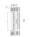
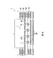
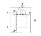
图3A~图3C与图4A~图4C为本发明一实施例的线路板的制造工艺剖面图。图5为图3A~图3C与图4A~图4C的基板的线路层与第二激光阻挡结构的俯视图。图6为图3A~图3C与图4A~图4C的基板的第一激光阻挡结构的俯视图。 3A-3C and 4A-4C are cross-sectional views of the manufacturing process of the circuit board according to an embodiment of the present invention. FIG. 5 is a top view of the circuit layer and the second laser blocking structure of the substrate of FIGS. 3A-3C and FIGS. 4A-4C . FIG. 6 is a top view of the first laser blocking structure of the substrate of FIGS. 3A-3C and FIGS. 4A-4C . the
值得注意的是,图5中剖面线I-I’的位置对应图6中剖面线I-I’的位置,且图3A~图3C为本发明一实施例的线路板制造工艺沿图5与图6中剖面线I-I’的剖面图。图5中剖面线II-II’的位置对应图6中剖面线II-II’的位置,且图4A~图4C为本发明一实施例的线路板制造工艺沿图5与 图6中剖面线II-II’的剖面图。 It should be noted that the position of section line II' in FIG. 5 corresponds to the position of section line II' in FIG. The sectional view of section line II' in Fig. 6 . The position of section line II-II' in Fig. 5 corresponds to the position of section line II-II' in Fig. 6, and Fig. 4A~Fig. Sectional view of II-II'. the
首先,请同时参阅图3A、图4A、图5与图6所示,提供一基板S,基板S具有一预移除区L。基板S包括一第一介电层310、一第一激光阻挡结构320、一第二介电层330、一线路层340、一第二激光阻挡结构350以及一第三介电层360。 First, please refer to FIG. 3A , FIG. 4A , FIG. 5 and FIG. 6 at the same time, a substrate S is provided, and the substrate S has a pre-removal area L. As shown in FIG. The substrate S includes a first
第一激光阻挡结构320配置于第一介电层310的一第一表面312,且位于预移除区L边缘。第二介电层330配置于第一介电层310上,并覆盖第一激光阻挡结构320。线路层340配置于第二介电层330的一第二表面332上,且部分线路层340由预移除区L外延伸进预移除区L内。 The first
第二激光阻挡结构350配置于第二表面332上并位于预移除区L边缘,且与线路层340绝缘,第二激光阻挡结构350与线路层340之间存在多个间隙G,且间隙G在第一表面312上的垂直投影与第一激光阻挡结构320重叠。 The second
第三介电层360配置于第二介电层330上,并覆盖线路层340与第二激光阻挡结构350。在本实施例中,基板S还包括一配置于第三介电层360上的一第四介电层370。 The third
接着,请同时参阅图3B、图4B、图5与图6所示,进行一激光加工制造工艺,以蚀刻位于预移除区L边缘的第三介电层360与第四介电层370。激光加工制造工艺在第三介电层360与第四介电层370上形成多个凹槽T,且这些凹槽T暴露出位于预移除区L边缘的第二激光阻挡层350与线路层340。 Next, referring to FIG. 3B , FIG. 4B , FIG. 5 and FIG. 6 , a laser manufacturing process is performed to etch the third
具体而言,激光加工是作用在预移除区L的边缘(即图5与图6中标示为L的虚线之处)。因此,当激光穿过第三与第四介电层360、370后,会被第二激光阻挡结构350阻挡。如此一来,本实施例可利用第二激光阻挡结构350来控制激光加工的深度,进而提升制造工艺良率。 Specifically, the laser processing is performed on the edge of the pre-removal area L (ie the dotted line marked L in FIGS. 5 and 6 ). Therefore, when the laser light passes through the third and fourth
此外,为提升第二激光阻挡结构350阻挡激光加工的效果,本实施例的第二激光阻挡结构350的宽度D大于激光光束的径度。因此,在较佳的情况下,凹槽T仅暴露出第二激光阻挡结构350的位于预移除区L边缘的部分。 In addition, in order to improve the effect of the second
值得注意的是,由于本实施例的基板S具有第一激光阻挡结构320,故当激光穿过间隙G下方的第二介电层330时,会被间隙G下方的第一激光阻挡结构320阻挡。因此,第一激光阻挡结构320可保护其下的第一介电层310免于受到激光加工的影响,并有助于控制激光加工的深度。此时,激光加工制造工艺例如是在间隙G下方的第二介电层330上形成凹槽334。 It should be noted that since the substrate S of this embodiment has the first
然后,请同时参阅图3C、图4C、图5与图6所示,移除第三介电层360与第四介电层370的位于预移除区L内的部分,而形成一移除区L1,其中,移除第三与第四介电层360、370的方法包括剥除法(lift off)。在本实施例中,基板S还包括一保护层380,其覆盖线路层340的位于移除区L1内 的部分,以保护线路层340免于受到移除第三与第四介电层360、370的影响。 Then, please refer to FIG. 3C, FIG. 4C, FIG. 5, and FIG. Region L1, wherein the method for removing the third and fourth
以下将就线路板300的结构部分作详细地介绍。 The structure of the
请同时参阅图3C、图4C、图5与图6所示,本实施例的线路板300具有一移除区L1,移除区L1为一凹陷区域。线路板300包括一第一介电层310、一第一激光阻挡结构320、一第二介电层330、一线路层340、一第二激光阻挡结构350以及一第三介电层360。 Please refer to FIG. 3C , FIG. 4C , FIG. 5 and FIG. 6 at the same time, the
第一激光阻挡结构320配置于第一介电层310的一第一表面312,且位于移除区L1边缘。第二介电层330配置于第一介电层310上,并覆盖第一激光阻挡结构320。线路层340配置于第二介电层330的一第二表面332上,且部分线路层340由移除区L1外延伸进移除区L1内。 The first
在本实施例中,线路板300包括多个第三激光阻挡结构390,第三激光阻挡结构390配置于第二表面332上并位于移除区L1边缘,第三激光阻挡结构390与线路层340的位于移除区L1边缘的部分相连,并与第二激光阻挡结构350绝缘。 In this embodiment, the
第二激光阻挡结构350配置于第二表面332上并位于移除区L1边缘,且第二激光阻挡结构350与线路层340绝缘。第二激光阻挡结构350与线路层340之间存在多个间隙G,间隙G在第一表面312上的垂直投影与第一激光阻挡结构320重叠。 The second
为提升第一激光阻挡结构320阻挡激光加工的效果,本实施例的第一激光阻挡结构320的尺寸可大于间隙G在第一表面312上的垂直投影面积,以使间隙G在第一表面312上的垂直投影可完全落在第一激光阻挡结构320上。另外,在本实施例中,第二介电层330可具有多个凹槽334,且凹槽334位于间隙G下方。凹槽334可暴露出第一激光阻挡结构320。 In order to improve the effect of the first
具体而言,在本实施例中,第二激光阻挡结构350为一环状结构,环状结构可具有多个缺口B,且部分线路层340由缺口B延伸进移除区L1内。此外,在本实施例中,第一激光阻挡结构320可为多个彼此独立的点状结构。在其他实施例中,第一激光阻挡结构320可为一条状结构或一环状结构,且条状结构或环状结构可与第二激光阻挡结构350在第一表面312上的垂直投影重叠。 Specifically, in this embodiment, the second
第三介电层360配置于第二介电层330上,并具有对应移除区L1的一开口O。在本实施例中,线路板300还包括一第四介电层370,且第四介电层370配置于第三介电层360上,并具有对应开口O的一开口O1。开口O、O1暴露出线路层340的位于移除区L1内的部分以及第二激光阻挡结构350的位于移除区L1内的部分。此外,在本实施例中,可在移除区L1内配置一保护层380,其覆盖线路层340的位于移除区L1内的部分,以保护开口O、O1 所暴露的线路层340。 The third
值得注意的是,本实施例是以一移除区L1为例,但并非用以限定本发明。举例来说,在其他未绘示的实施例中,线路板亦可具有多个移除区,且这些移除区可选择性地位于线路板的同一侧或者是位于线路板的相对两侧。 It should be noted that this embodiment takes a removal area L1 as an example, but it is not intended to limit the present invention. For example, in other unillustrated embodiments, the circuit board can also have multiple removal areas, and these removal areas can be selectively located on the same side of the circuit board or on opposite sides of the circuit board. the
综上所述,由于本发明的线路板具有第一与第二激光阻挡结构,故本发明可利用第二激光阻挡结构来控制激光加工的深度。并且,可利用第一激光阻挡结构保护其下的第一介电层免于受到激光加工的影响。 To sum up, since the circuit board of the present invention has the first and second laser blocking structures, the present invention can use the second laser blocking structure to control the depth of laser processing. Also, the first laser blocking structure can be used to protect the underlying first dielectric layer from being affected by laser processing. the
以上所述,仅是本发明的较佳实施例而已,并非对本发明作任何形式上的限制,虽然本发明已以较佳实施例揭露如上,然而并非用以限定本发明,任何熟悉本专业的技术人员,在不脱离本发明技术方案范围内,当可利用上述揭示的方法及技术内容作出些许的更动或修饰为等同变化的等效实施例,但凡是未脱离本发明技术方案的内容,依据本发明的技术实质对以上实施例所作的任何简单修改、等同变化与修饰,均仍属于本发明技术方案的范围内。 The above description is only a preferred embodiment of the present invention, and does not limit the present invention in any form. Although the present invention has been disclosed as above with preferred embodiments, it is not intended to limit the present invention. Anyone familiar with this field Those skilled in the art, without departing from the scope of the technical solution of the present invention, may use the method and technical content disclosed above to make some changes or modifications to equivalent embodiments with equivalent changes, but if they do not depart from the technical solution of the present invention, Any simple modifications, equivalent changes and modifications made to the above embodiments according to the technical essence of the present invention still fall within the scope of the technical solution of the present invention. the
Claims (17)
Translated fromChinesePriority Applications (1)
| Application Number | Priority Date | Filing Date | Title |
|---|---|---|---|
| CN2009101344852ACN101868116B (en) | 2009-04-20 | 2009-04-20 | Circuit board and manufacturing method thereof |
Applications Claiming Priority (1)
| Application Number | Priority Date | Filing Date | Title |
|---|---|---|---|
| CN2009101344852ACN101868116B (en) | 2009-04-20 | 2009-04-20 | Circuit board and manufacturing method thereof |
Publications (2)
| Publication Number | Publication Date |
|---|---|
| CN101868116A CN101868116A (en) | 2010-10-20 |
| CN101868116Btrue CN101868116B (en) | 2012-05-23 |
Family
ID=42959609
Family Applications (1)
| Application Number | Title | Priority Date | Filing Date |
|---|---|---|---|
| CN2009101344852AActiveCN101868116B (en) | 2009-04-20 | 2009-04-20 | Circuit board and manufacturing method thereof |
Country Status (1)
| Country | Link |
|---|---|
| CN (1) | CN101868116B (en) |
Families Citing this family (3)
| Publication number | Priority date | Publication date | Assignee | Title |
|---|---|---|---|---|
| US8692111B2 (en)* | 2011-08-23 | 2014-04-08 | Sunpower Corporation | High throughput laser ablation processes and structures for forming contact holes in solar cells |
| TWI661476B (en)* | 2018-02-14 | 2019-06-01 | 頎邦科技股份有限公司 | Semiconductor substrate and processing method thereof |
| CN110620053B (en)* | 2019-09-06 | 2021-09-03 | 广东佛智芯微电子技术研究有限公司 | Fan-out type packaging structure with laser opening blocking layer and preparation method thereof |
- 2009
- 2009-04-20CNCN2009101344852Apatent/CN101868116B/enactiveActive
Also Published As
| Publication number | Publication date |
|---|---|
| CN101868116A (en) | 2010-10-20 |
Similar Documents
| Publication | Publication Date | Title |
|---|---|---|
| TWI392404B (en) | Circuit board and manufacturing method thereof | |
| CN103676386B (en) | A kind of display floater and display device | |
| US20150171019A1 (en) | Semiconductor device and method of manufacturing the same | |
| TWI429072B (en) | Semiconductor device and method of manufacturing same | |
| TWI453513B (en) | Display panel | |
| JP6347814B2 (en) | Touch panel and manufacturing method thereof | |
| CN205881903U (en) | Walk line knot structure, array substrate and display device | |
| CN109003944B (en) | Method for manufacturing a substrate, substrate, and display device | |
| CN101868116B (en) | Circuit board and manufacturing method thereof | |
| CN210052016U (en) | Photomask and exposure device | |
| US9543247B1 (en) | Surface-mount electronic component | |
| US20120219701A1 (en) | Method for fabricating touch sensor structure | |
| CN103915450A (en) | Array substrate, manufacturing method and display device | |
| US8298961B2 (en) | Patterns of semiconductor device and method of forming the same | |
| US9806109B2 (en) | Half tone mask plate and method for manufacturing array substrate using the same | |
| CN201766768U (en) | Circuit board with removal area | |
| CN108140646A (en) | Array substrate manufacturing method | |
| KR20110103881A (en) | Semiconductor device and manufacturing method thereof | |
| KR20130004680A (en) | Method of manufacturing a dram device | |
| CN107134466B (en) | Flexible panel and manufacturing method thereof | |
| TWI549243B (en) | Semiconductor structure and manufacturing method thereof | |
| EP3288079B1 (en) | Array substrate and preparation method therefor, display panel, and display device | |
| TWI703906B (en) | Method for reducing residual dry film on a printed circuit board | |
| US20130026641A1 (en) | Conductor contact structure and forming method, and photomask pattern generating method for defining such conductor contact structure | |
| TWI406616B (en) | Passive components and their methods |
Legal Events
| Date | Code | Title | Description |
|---|---|---|---|
| C06 | Publication | ||
| PB01 | Publication | ||
| C10 | Entry into substantive examination | ||
| SE01 | Entry into force of request for substantive examination | ||
| C14 | Grant of patent or utility model | ||
| GR01 | Patent grant |