CN101866995B - Light-emitting diode packaging structure - Google Patents
Light-emitting diode packaging structureDownload PDFInfo
- Publication number
- CN101866995B CN101866995BCN200910132740XACN200910132740ACN101866995BCN 101866995 BCN101866995 BCN 101866995BCN 200910132740X ACN200910132740X ACN 200910132740XACN 200910132740 ACN200910132740 ACN 200910132740ACN 101866995 BCN101866995 BCN 101866995B
- Authority
- CN
- China
- Prior art keywords
- light
- led
- bearing substrate
- package structure
- emitting diode
- Prior art date
- Legal status (The legal status is an assumption and is not a legal conclusion. Google has not performed a legal analysis and makes no representation as to the accuracy of the status listed.)
- Active
Links
Images


Classifications
- H—ELECTRICITY
- H01—ELECTRIC ELEMENTS
- H01L—SEMICONDUCTOR DEVICES NOT COVERED BY CLASS H10
- H01L2224/00—Indexing scheme for arrangements for connecting or disconnecting semiconductor or solid-state bodies and methods related thereto as covered by H01L24/00
- H01L2224/01—Means for bonding being attached to, or being formed on, the surface to be connected, e.g. chip-to-package, die-attach, "first-level" interconnects; Manufacturing methods related thereto
- H01L2224/42—Wire connectors; Manufacturing methods related thereto
- H01L2224/47—Structure, shape, material or disposition of the wire connectors after the connecting process
- H01L2224/48—Structure, shape, material or disposition of the wire connectors after the connecting process of an individual wire connector
- H01L2224/4805—Shape
- H01L2224/4809—Loop shape
- H01L2224/48091—Arched
- H—ELECTRICITY
- H01—ELECTRIC ELEMENTS
- H01L—SEMICONDUCTOR DEVICES NOT COVERED BY CLASS H10
- H01L2224/00—Indexing scheme for arrangements for connecting or disconnecting semiconductor or solid-state bodies and methods related thereto as covered by H01L24/00
- H01L2224/01—Means for bonding being attached to, or being formed on, the surface to be connected, e.g. chip-to-package, die-attach, "first-level" interconnects; Manufacturing methods related thereto
- H01L2224/42—Wire connectors; Manufacturing methods related thereto
- H01L2224/47—Structure, shape, material or disposition of the wire connectors after the connecting process
- H01L2224/49—Structure, shape, material or disposition of the wire connectors after the connecting process of a plurality of wire connectors
- H01L2224/491—Disposition
- H01L2224/49105—Connecting at different heights
- H01L2224/49107—Connecting at different heights on the semiconductor or solid-state body
- H—ELECTRICITY
- H01—ELECTRIC ELEMENTS
- H01L—SEMICONDUCTOR DEVICES NOT COVERED BY CLASS H10
- H01L2224/00—Indexing scheme for arrangements for connecting or disconnecting semiconductor or solid-state bodies and methods related thereto as covered by H01L24/00
- H01L2224/73—Means for bonding being of different types provided for in two or more of groups H01L2224/10, H01L2224/18, H01L2224/26, H01L2224/34, H01L2224/42, H01L2224/50, H01L2224/63, H01L2224/71
- H01L2224/732—Location after the connecting process
- H01L2224/73251—Location after the connecting process on different surfaces
- H01L2224/73265—Layer and wire connectors
- H—ELECTRICITY
- H01—ELECTRIC ELEMENTS
- H01L—SEMICONDUCTOR DEVICES NOT COVERED BY CLASS H10
- H01L2924/00—Indexing scheme for arrangements or methods for connecting or disconnecting semiconductor or solid-state bodies as covered by H01L24/00
- H01L2924/15—Details of package parts other than the semiconductor or other solid state devices to be connected
- H01L2924/181—Encapsulation
Landscapes
- Led Device Packages (AREA)
Abstract
Description
Translated fromChinese技术领域technical field
本发明涉及一种发光二极管封装结构,且特别是涉及一种具有高导热效率的发光二极管封装结构。The invention relates to a light-emitting diode packaging structure, and in particular to a light-emitting diode packaging structure with high heat conduction efficiency.
背景技术Background technique
近年来,由于发光二极管的发光效率不断提升,使得发光二极管开始广泛被使用于许多照明应用中,例如需要高速反应的扫描器灯源、液晶显示器的背光源或前光源汽车的仪表板照明、交通号志灯,以及一般的照明装置等。发光二极管的发光原理是将电能转换为光,也就是对发光二极管施加电流,通过电子、空穴的结合以光的型态释放出来,进而达到发光的效果。In recent years, due to the continuous improvement of the luminous efficiency of light-emitting diodes, light-emitting diodes have been widely used in many lighting applications, such as scanner light sources that require high-speed response, backlight or front light sources for liquid crystal displays, instrument panel lighting for vehicles, traffic Signal lights, and general lighting installations, etc. The light-emitting principle of light-emitting diodes is to convert electrical energy into light, that is, to apply current to the light-emitting diodes, and release them in the form of light through the combination of electrons and holes, thereby achieving the effect of light.
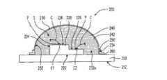
图1绘示已知发光二极管封装结构的剖面图。请参照图1,已知的发光二极管封装结构100由发光二极管芯片110、承载基板120、导线132、导线134以及封装胶体140构成。其中,发光二极管芯片110设置于承载基板120上,而且导线132、导线134分别电性连接于发光二极管芯片110与承载基板120之间。封装胶体140设置于承载基板120上并包覆导线132、导线134。发光二极管芯片110主要是通过对两条导线132、导线134施加电压差以使发光二极管芯片110的有源层112发光,同时有源层112也会产生热量,若发光二极管芯片110的有源层112发光时所产生的热量无法有效排出,特别在高电流驱使下时,发光二极管芯片110往往容易因过热而损坏。FIG. 1 is a cross-sectional view of a known LED package structure. Referring to FIG. 1 , a known
发明内容Contents of the invention
本发明提供一种发光二极管封装结构,特别是一种发光二极管的封装散热结构,以提升封装整体导热效率。The invention provides a packaging structure of a light emitting diode, in particular a heat dissipation structure of a packaging of a light emitting diode, so as to improve the overall heat conduction efficiency of the packaging.
本发明提出一种发光二极管封装结构包括承载基板、至少一发光二极管芯片、光学元件以及高导热透光液体。发光二极管芯片配置于承载基板上,并具有有源层。光学元件配置于承载基板上,光学元件与承载基板之间形成封闭空间,且发光二极管芯片位于封闭空间中。高导热透光液体填满于封闭空间中。其中,相对于发光二极管芯片所发出的主波长的光,高导热透光液体的光穿透率大于80%,高导热透光液体的导热系数大于环氧树脂的导热系数。The present invention proposes a light emitting diode packaging structure including a carrier substrate, at least one light emitting diode chip, an optical element, and a highly thermally conductive and light-transmitting liquid. The light emitting diode chip is configured on the carrier substrate and has an active layer. The optical element is arranged on the carrying substrate, a closed space is formed between the optical element and the carrying substrate, and the LED chip is located in the closed space. High thermal conductivity and light-transmitting liquid is filled in the closed space. Wherein, relative to the light of the main wavelength emitted by the light-emitting diode chip, the light transmittance of the high thermal conductivity and light-transmitting liquid is greater than 80%, and the thermal conductivity of the high-thermal-conduction and light-transmitting liquid is greater than that of epoxy resin.
本发明提出一种发光二极管封装结构包括承载基板、至少一凸起部、至少一发光二极管芯片、光学元件以及高导热透光液体。凸起部配置于承载基板上,并具有开口以暴露出承载基板,且凸起部的材料为导热材料。发光二极管芯片配置于承载基板上并位于开口中,且开口截面的宽度与发光二极管芯片截面的宽度比值为1至1.5。光学元件配置于承载基板上,光学元件与承载基板之间形成封闭空间,且凸起部与发光二极管芯片位于封闭空间中。高导热透光液体填满于封闭空间中。其中,相对于发光二极管芯片所发出的主波长的光,高导热透光液体的光穿透率大于80%,高导热透光液体的导热系数大于环氧树脂的导热系数。The present invention proposes a light emitting diode packaging structure including a carrier substrate, at least one raised portion, at least one light emitting diode chip, an optical element, and a highly thermally conductive and light-transmitting liquid. The protruding part is arranged on the carrying substrate and has an opening to expose the carrying substrate, and the material of the protruding part is a heat-conducting material. The light emitting diode chip is arranged on the carrier substrate and located in the opening, and the ratio of the width of the cross section of the opening to the width of the cross section of the light emitting diode chip is 1 to 1.5. The optical element is arranged on the carrying substrate, a closed space is formed between the optical element and the carrying substrate, and the protruding part and the LED chip are located in the closed space. High thermal conductivity and light-transmitting liquid is filled in the closed space. Wherein, relative to the light of the main wavelength emitted by the light-emitting diode chip, the light transmittance of the high thermal conductivity and light-transmitting liquid is greater than 80%, and the thermal conductivity of the high-thermal-conduction and light-transmitting liquid is greater than that of epoxy resin.
本发明提出一种发光二极管封装结构包括承载基板、至少一垫高部、至少一发光二极管芯片、光学元件、高导热透光液体以及密封元件。垫高部配置于承载基板上,具有至少一沟槽与远离承载基板的第一顶面,且垫高部的材料为导热材料。发光二极管芯片配置于垫高部的第一顶面上。光学元件配置于承载基板上,光学元件与承载基板之间形成封闭空间,且垫高部与发光二极管芯片位于封闭空间中。高导热透光液体填满于封闭空间中,并填满于沟槽中。其中,相对于发光二极管芯片所发出的主波长的光,高导热透光液体的光穿透率大于80%,高导热透光液体的导热系数大于环氧树脂的导热系数。The invention proposes a light emitting diode packaging structure including a carrier substrate, at least one pad, at least one light emitting diode chip, an optical element, a highly heat-conductive and light-transmitting liquid, and a sealing element. The raised portion is disposed on the carrier substrate, has at least one groove and a first top surface away from the carrier substrate, and the material of the raised portion is a heat-conducting material. The light emitting diode chip is configured on the first top surface of the raised part. The optical element is arranged on the carrying substrate, and a closed space is formed between the optical element and the carrying substrate, and the raised part and the LED chip are located in the closed space. The highly thermally conductive and light-transmitting liquid is filled in the closed space and filled in the grooves. Wherein, relative to the light of the main wavelength emitted by the light-emitting diode chip, the light transmittance of the high thermal conductivity and light-transmitting liquid is greater than 80%, and the thermal conductivity of the high-thermal-conduction and light-transmitting liquid is greater than that of epoxy resin.
基于上述,本发明的高导热透光液体填满于封闭空间中,因此,发光二极管芯片不仅可通过承载基板提升其底部的导热效率,还可通过高导热透光液体提升其侧壁与顶面的导热效率。Based on the above, the high thermal conductivity and light-transmitting liquid of the present invention is filled in the closed space, therefore, the light-emitting diode chip can not only improve the heat conduction efficiency of its bottom through the carrier substrate, but also improve its side wall and top surface through the high heat-conducting and light-transmitting liquid thermal conductivity.
为让本发明的上述特征和优点能更明显易懂,下文特举实施例,并配合附图作详细说明如下。In order to make the above-mentioned features and advantages of the present invention more comprehensible, the following specific embodiments are described in detail with reference to the accompanying drawings.
附图说明Description of drawings
图1绘示已知发光二极管封装结构的剖面图。FIG. 1 is a cross-sectional view of a known LED package structure.
图2绘示本发明实施例的发光二极管封装结构的剖面图。FIG. 2 is a cross-sectional view of an LED packaging structure according to an embodiment of the present invention.
图3绘示图2的发光二极管封装结构的一种变化型。FIG. 3 illustrates a modification of the LED package structure in FIG. 2 .
图4A绘示本发明实施例的发光二极管封装结构的剖面图。FIG. 4A is a cross-sectional view of an LED packaging structure according to an embodiment of the present invention.
图4B绘示图4A的发光二极管封装结构的一种变化。FIG. 4B illustrates a variation of the LED package structure shown in FIG. 4A .
图5绘示本发明实施例的发光二极管封装结构的剖面图。FIG. 5 is a cross-sectional view of an LED packaging structure according to an embodiment of the present invention.
图6A与图6B绘示图5的发光二极管封装结构的二种变化型。6A and 6B illustrate two variants of the LED package structure shown in FIG. 5 .
附图标记说明Explanation of reference signs
100、200、400、500:发光二极管封装结构100, 200, 400, 500: LED packaging structure
110、220:发光二极管芯片110, 220: LED chip
112:有源层112: active layer
114、222:底面114, 222: bottom surface
116、224:侧壁116, 224: side wall
118、226:顶面118, 226: top surface
120、210:承载基板120, 210: carrying substrate
132、134、C:导线132, 134, C: Wire
140:封装胶体140: encapsulation colloid
212:表面212: surface
230:光学元件230: Optics
232:凹槽232: Groove
232a:开放端232a: Open end
234:外缘234: outer edge
240:高导热透光液体240: High thermal conductivity and light-transmitting liquid
242:悬浮粒子242: Suspended particles
250:密封元件250: sealing element
252:第二顶面252: second top surface
260:连接层260: Connection layer
270:固定组件270: Fixed components
280、F:粘着层280, F: Adhesive layer
290:反射层290: reflective layer
410、516:凸起部410, 516: convex part
510:垫高部510: Padded part
512:第一顶面512: first top surface
514:底部514: Bottom
A:内壁A: inner wall
D:深度D: Depth
E1、E2:电极E1, E2: electrodes
G:间隙G: Gap
H1、H2:距离H1, H2: Distance
OP:开口OP: open
P:接垫P: Pad
S:封闭空间S: closed space
T:沟槽T: Groove
W1、W2、W3、W4:宽度W1, W2, W3, W4: Width
具体实施方式Detailed ways
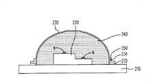
图2绘示本发明实施例的发光二极管封装结构的剖面图。请参照图2,发光二极管封装结构200包括承载基板210、发光二极管芯片220、光学元件230以及高导热透光液体240。FIG. 2 is a cross-sectional view of an LED packaging structure according to an embodiment of the present invention. Please refer to FIG. 2 , the
承载基板210例如是高导热基板,其中高导热基板例如是氧化铝基板(Al2O3)、氮化铝基板(AlN)、铜基板、铝基板等具有良好热导性质的基板。在本实施例中,高导热基板的导热系数例如是大于25W/mK。发光二极管芯片220配置于承载基板210上,并具有有源层(未绘示)。在本实施例中,若需产生特定色光(如白光)时,可选择性地在发光二极管芯片220的出光路径上形成光转换层(未绘示)。详细而言,光转换层可以是直接覆盖于发光二极管芯片220的表面,以增加光均匀性,另外,光转换层也可以是非直接贴覆于发光二极管芯片表面,如此可避免光转换层因芯片的热产生黄化。此外,为提升承载基板210的散热效率,可选择性地在承载基板210的远离发光二极管芯片220的表面212配置散热器(未绘示)。The
光学元件230配置于承载基板210上,光学元件230与承载基板210之间形成封闭空间S,且发光二极管芯片220位于封闭空间S中。具体而言,在本实施例中,光学元件230为弧形光学元件,光学元件230具有凹槽232,且承载基板210配置于凹槽232的开放端232a上,以密封凹槽232并形成封闭空间S。光学元件230的材料例如为玻璃等透光性质良好的材料,光学元件230例如为透镜。在本实施例中,光学元件230相对于发光二极管芯片220所发出的(部分或全部)光的波长而言是可穿透的,例如光学元件230相对于可见光的波长而言是可穿透的。The
光学元件230的材料例如为玻璃、环氧树脂或透明塑料,其中透明塑料为烯烃族(olefinic)的透明塑料或是脂肪族(aliphatic)的透明塑料(例如聚丙烯或聚乙烯),且前述透明塑料在接触非质子性溶剂(例如含有丙烯碳酸盐的溶液)时,不易劣化。透明塑料例如为环状烯烃共聚物(cyclic olefincopolymer)、聚甲基戊烯(polymethylpentenes)、氢化环烯烃聚合物(hydrogenated cyclo-olefin polymers)或是非晶的环烯烃共聚物(amorphouscyclo-olefin copolymers)。The material of the
高导热透光液体240填满于封闭空间S中,其为具备高热传导性及流动性的液体。在本实施例中,高导热透光液体240的导热系数(thermalconductivity)大于环氧树脂(epoxy)的导热系数,且当相对于发光二极管芯片220所发出的主波长的光时,高导热透光液体240的光穿透率(transmittance)大于80%。因此,高导热透光液体240可直接接触承载基板210、光学元件230与发光二极管芯片220的暴露于封闭空间S中的全部表面。如此一来,可通过高导热透光液体240的流动将发光二极管芯片220在发光时所产生的热传导至承载基板210与光学元件230,并经由承载基板210与光学元件230传导至发光二极管封装结构200外。值得注意的是,在本实施例中,发光二极管芯片220不仅可通过承载基板210提升其底面222的导热效率,还可通过高导热透光液体240提升其侧壁224与顶面226的导热效率。The high thermal conductivity and
在本实施例中,为避免高导热透光液体240使发光二极管芯片220的二电极E1、E2之间电性短路,高导热透光液体240例如是不导电液体。高导热透光液体240的材料是选自硅油(silicon oils)、白蜡油(paraffin oils)、橄榄油(olive oils)、碳酸丙烯脂(propylene carbonate)、全氟聚醚液其中之一或是其他具备高热传导性与流动性的液体。值得注意的是,当高导热透光液体240具有导电性时,可在发光二极管芯片220的导电的部分(例如接垫P)、发光二极管芯片220的电性连接的部分(例如导线C)以及发光二极管芯片220侧壁有源层的部分上形成隔绝层(其材料例如是绝缘材料),隔绝层可隔绝高导热透光液体240以避免高导热透光液体240造成元件短路,例如利用光转换层来包裹发光二极管芯片220以形成隔绝层。In this embodiment, in order to avoid the electrical short circuit between the two electrodes E1 and E2 of the
在本实施例中,高导热透光液体240可掺杂有多个悬浮粒子242,举例来说,高导热透光液体240例如是掺杂有二氧化钛粒子的去离子水(deionizedwater)。由于悬浮粒子242可增加发光二极管芯片220所发出的光线的折射与反射,故可有效提高出光角度,以避免光线直接射入人眼所造成的不适。In this embodiment, the high thermal conductivity
高导热透光液体240为在室温下具有流动性的液体,其粘滞系数例如是小于10000mPas。在本实施例中,为避免高导热透光液体240在低温下结冻,可在高导热透光液体240中添加抗冻材料,以维持其流动性,抗冻材料例如甲醇或乙二醇。The high thermal conductivity and light-transmitting
此外,发光二极管封装结构200可选择性地具有密封元件250。密封元件250连接光学元件230的外缘234与承载基板210,且位于封闭空间S外,密封元件250的材料例如是金属或合金,其中前述合金例如是铁钴镍合金(商业上名为Kovar alloy)。密封元件250连接承载基板210的方式例如是金属与金属之间相互连接,故密封元件250连接承载基板210的可靠度佳。In addition, the
在本实施例中,列举下列三种连接光学元件230与密封元件250的方法,但并非用以限定本发明。方法1是将光学元件230加热至其玻璃转换温度或软化温度,再使密封元件250镶在光学元件230的外缘234上。方法2是先将光学元件230的外缘234金属化(例如镀金属,例如钛),然后,利用焊料(未绘示)接合光学元件230与密封元件250。方法3是利用密封胶(未绘示)接合光学元件230与密封元件250,前述密封胶的特性接近玻璃,且具有较低的软化温度(例如低于700℃)。In this embodiment, the following three methods for connecting the
在本实施例中,列举下列二种连接承载基板210与密封元件250的方法,但并非用以限定本发明。方法1是利用连接层260连接密封元件250与承载基板210,连接层260是位于密封元件250与承载基板210之间,且其材料例如是金属或合金(例如焊料)。连接层260的形状可以对应密封元件250的横剖面形状而设计为圆形、四边形、椭圆形等,且连接层260可提高密封元件250与承载基板210间的接合力,进而提高封装整体的可靠度。具体而言,可先在承载基板210上形成焊料,之后再将已与光学元件230连接的密封元件250配置于焊料上并加热焊料。In this embodiment, the following two methods for connecting the
图3绘示图2的发光二极管封装结构的一种变化型。请参照图3,方法2为先在承载基板210上形成固定在承载基板210上的固定组件270。固定组件270固定在承载基板210上的方式例如是通过焊料(未绘示)接合至承载基板210、通过胶材(未绘示)粘着至承载基板210,或是通过固定组件270与陶瓷粉末共同烧结的方式接合、或者是固定组件270与承载基板210为一体成型。然后,将已与光学元件230连接的密封元件250配置于固定组件270上。之后,以例如尖端放电(point discharge)或激光焊接(laser welding)的方式加热密封元件250与固定组件270相接的部分。固定组件270的材料可以为与密封元件250相同材料,例如铁钴镍合金或Invar不胀钢。FIG. 3 illustrates a modification of the LED package structure in FIG. 2 . Referring to FIG. 3 , method 2 is to firstly form a
图4A绘示本发明实施例的发光二极管封装结构的剖面图,图4B绘示图4A的发光二极管封装结构的一种变化型。请参照图4A,本实施例的发光二极管封装结构400包括承载基板210、凸起部410、发光二极管芯片220、光学元件230以及高导热透光液体240。此外,发光二极管封装结构400可选择性地具有密封元件250。FIG. 4A is a cross-sectional view of an LED packaging structure according to an embodiment of the present invention, and FIG. 4B is a modification of the LED packaging structure shown in FIG. 4A . Please refer to FIG. 4A , the
值得注意的是,发光二极管封装结构400与图2的发光二极管封装结构200相似,差异之处仅在于发光二极管封装结构400额外具有凸起部410。因此,下述仅就两者的差异之处进行详细介绍,而两者相同之处则不再赘述。It should be noted that the
凸起部410配置于承载基板210上,并具有开口OP以暴露出承载基板210。凸起部410的材料为导热材料,导热材料可以是金属或是金属合金,例如是金、银、铜、铟、钛、锌、铝、铅、锡、镍、铂、铬,或者是具有良好导热材料的复合材料,例如是陶瓷。The protruding
发光二极管芯片220配置于承载基板210上并位于开口OP中。凸起部410与发光二极管芯片220皆位于由光学元件230与承载基板210所构成的封闭空间S中,且高导热透光液体240可直接接触承载基板210、光学元件230、发光二极管芯片220与凸起部410的暴露于封闭空间S中的全部表面。The
在其他实施例中,若需产生特定色光,则可增加开口OP的深度D(即增加凸起部410的厚度),使开口OP的深度D大于发光二极管芯片220的高度(也就是使发光二极管芯片220的顶面低于凸起部410的顶面),并在开口OP中填入荧光粉。In other embodiments, if a specific color light needs to be generated, the depth D of the opening OP can be increased (that is, the thickness of the protruding
开口OP截面的宽度W1与发光二极管芯片220截面的宽度W2的比值为1至1.5。值得注意的是,在本实施例中,开口OP截面的宽度W1与发光二极管芯片220截面的宽度W2是指在同一剖面时,开口OP的(最小)宽度W1与发光二极管芯片220的(最大)宽度W2。The ratio of the width W1 of the section of the opening OP to the width W2 of the section of the
由前述可知,凸起部410贴近发光二极管芯片220的侧壁224,因此,可通过凸起部410增加发光二极管芯片220的侧壁224的导热效率。It can be seen from the foregoing that the protruding
图4A绘示的凸起部410的开口OP截面的宽度W1与发光二极管芯片220截面的宽度W2的比值大于1并小于等于1.5,换言之,在发光二极管芯片220的侧壁224与凸起部410之间可存在间隙G,且粘着层F可填满于间隙G中,粘着层F的材料例如为银胶、焊锡、玻璃以及合金或是其他适合的导热材料。此外,当开口OP截面的宽度与发光二极管芯片220截面的宽度比值为大于1并小于等于1.5时,凸起部410与承载基板210例如是一体成型或是各自成型。换言之,凸起部410与承载基板210可以是同时形成,或者是各自成型后再将凸起部410组装至承载基板210上。当凸起部410与承载基板210为各自成型时,凸起部410的材料例如与承载基板210相同皆为高热导系数材料,或者是与承载基板210的材料相异的其它具有导热功能的材料,又或者是与承载基板210的材料部分相同的材料。The ratio of the width W1 of the section width W1 of the opening OP of the
另外,请参照图4B,在本实施例中,可在间隙G中以及发光二极管芯片220与承载基板210之间设置粘着层280,以接合发光二极管芯片220至承载基板210以及凸起部410。粘着层280的材料例如是银胶、焊锡、玻璃以及合金或是其他适合的导热材料,因此,粘着层280可有助于提升发光二极管芯片220的导热效率。In addition, please refer to FIG. 4B , in this embodiment, an
由前述可知,在本实施例中,发光二极管芯片220可将(发光二极管芯片220于发光时所产生的)热传导至下方承载基板210,或者是通过凸起部410与高导热透光液体240接触,使热经由承载基板210与高导热透光液体240传导至发光二极管封装结构400外,以提升发光二极管芯片220的导热效率。It can be seen from the foregoing that in this embodiment, the
另外,在本实施例中,可在开口OP的内壁A以及承载基板210的被开口OP所暴露出的部分上形成反射层290,以反射发光二极管芯片220所产生的光线进而提高光线的利用率,反射层290的材料例如是银或是其他适于反射光线的材料。在其他未绘示的实施例中,当发光二极管芯片220截面的宽度比值为1时,发光二极管芯片220的侧壁224与凸起部410贴合。In addition, in this embodiment, a
图5绘示本发明实施例的发光二极管封装结构的剖面图。图6A与图6B绘示图5的发光二极管封装结构的二种变化型。FIG. 5 is a cross-sectional view of an LED packaging structure according to an embodiment of the present invention. 6A and 6B illustrate two variants of the LED package structure shown in FIG. 5 .
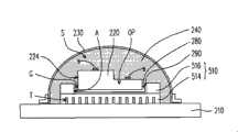
请参照图5,本实施例的发光二极管封装结构500包括承载基板210、垫高部510、发光二极管芯片220、光学元件230以及高导热透光液体240。此外,发光二极管封装结构500可选择性地具有密封元件250与固定组件(未绘示)。Referring to FIG. 5 , the
值得注意的是,发光二极管封装结构500与图2的发光二极管封装结构200相似,差异之处仅在于发光二极管封装结构500额外具有垫高部510。因此,下述仅就两者的差异之处进行详细介绍,而两者相同的处则不再赘述。It should be noted that the
垫高部510配置于承载基板210上,并具有多个沟槽T以及远离承载基板210的第一顶面512,且垫高部510的材料为导热材料。发光二极管芯片220配置于垫高部510的第一顶面512上,且垫高部510与发光二极管芯片220皆位于封闭空间S中。高导热透光液体240可直接接触承载基板210、光学元件230、发光二极管芯片220与垫高部510的暴露于封闭空间S中的全部表面,且高导热透光液体240可填满于沟槽T中。The
由于沟槽T可增加垫高部510与高导热透光液体240的接触面积,因此,当发光二极管芯片220产生的热传导至垫高部510时,可通过高导热透光液体240的流动移除传导至垫高部510的热,进而增加垫高部510的导热效率。Since the trench T can increase the contact area between the
密封元件250具有远离承载基板210的第二顶面252,垫高部510的第一顶面512与承载基板210之间的距离H1大于等于密封元件250的第二顶面252与承载基板210之间的距离H2。如此一来,可通过垫高部510垫高发光二极管芯片220,以避免发光二极管芯片220所发出的光线被密封元件250阻挡,进而提升发光二极管封装结构500的出光效率(light extractionefficiency)。The sealing
请参照图6A,在本实施例中,垫高部510包括底部514与凸起部516,凸起部516位于底部514上,且凸起部516具有开口OP以暴露出底部514,发光二极管芯片220配置于底部514上并位于开口OP中。开口OP截面的宽度W3与发光二极管芯片220截面的宽度W4比值例如为1至1.5。值得注意的是,由于凸起部516贴近发光二极管芯片220的侧壁224,故可通过凸起部516增加发光二极管芯片220的侧壁224的导热效率。Please refer to FIG. 6A. In this embodiment, the raised
图6A绘示的开口OP截面的宽度W3与发光二极管芯片220截面的宽度W4比值为大于1并小于等于1.5。换言之,发光二极管芯片220与凸起部516之间存在有间隙G,且粘着层F可填满于间隙G中,粘着层F的材料例如为银胶、焊锡、玻璃以及合金或是其他适合的导热材料。此时,可藉凸起部516与高导热透光液体240接触,来提升发光二极管芯片220的侧壁224的导热效率。底部514与凸起部516例如是一体成型。The ratio of the width W3 of the section of the opening OP to the width W4 of the section of the
另外,请参照图6B,在本实施例中,可在间隙G中以及发光二极管芯片220与底部514之间设置粘着层280,以接合发光二极管芯片220至底部514以及凸起部516。粘着层280的材料例如是银胶、焊锡、玻璃以及合金或是其他适合的导热材料,因此,粘着层280可有助于提升发光二极管芯片220的导热效率。In addition, please refer to FIG. 6B , in this embodiment, an
另外,在本实施例中,可在开口OP的内壁A以及底部514的被开口OP所暴露出的部分上形成反射层290,以反射发光二极管芯片220所产生的光线进而提高光线的利用率,反射层290的材料例如是银或是其他适于反射光线的材料。In addition, in this embodiment, a
在其他未绘示的实施例中,开口OP截面的宽度W3与发光二极管芯片220截面的宽度W4比值可为1,换言之,发光二极管芯片220与凸起部516贴合。此时,凸起部516可直接将发光二极管芯片220于发光时所产生的热传导至承载基板210,并经由承载基板210传导至发光二极管封装结构外,以提升发光二极管芯片220的侧壁224的导热效率。In other unillustrated embodiments, the ratio of the width W3 of the section of the opening OP to the width W4 of the section of the
综上所述,本发明的高导热透光液体填满于封闭空间中,因此,高导热透光液体可直接接触承载基板、光学元件与发光二极管芯片的暴露于封闭空间中的全部表面。如此一来,发光二极管芯片不仅可通过承载基板提升其底部的导热效率,还可通过高导热透光液体提升其侧壁与顶面的导热效率。本发明采用密封元件连接光学元件与承载基板,以将光学元件固定在承载基板上。此外,本发明利用贴近发光二极管芯片的侧壁的凸起部来增加发光二极管芯片的侧壁的导热效率。另外,本发明的垫高部可垫高发光二极管芯片,以避免发光二极管芯片所发出的光线被密封元件阻挡,进而提升发光二极管封装结构的出光效率。To sum up, the high thermal conductivity and light-transmitting liquid of the present invention is filled in the closed space. Therefore, the high heat-conducting and light-transmitting liquid can directly contact all surfaces of the carrier substrate, optical elements and LED chips exposed in the closed space. In this way, the light-emitting diode chip can not only improve the heat conduction efficiency of its bottom through the carrier substrate, but also improve the heat conduction efficiency of its side wall and top surface through the highly heat-conductive light-transmitting liquid. The invention adopts the sealing element to connect the optical element and the carrying substrate to fix the optical element on the carrying substrate. In addition, the present invention utilizes the protruding portion close to the sidewall of the LED chip to increase the heat conduction efficiency of the sidewall of the LED chip. In addition, the raised part of the present invention can raise the LED chip to prevent the light emitted by the LED chip from being blocked by the sealing element, thereby improving the light extraction efficiency of the LED packaging structure.
虽然本发明已以实施例披露如上,然其并非用以限定本发明,任何所属技术领域中普通技术人员,在不脱离本发明的精神和范围内,当可作些许的更动与润饰,故本发明的保护范围当视所附的权利要求界定者为准。Although the present invention has been disclosed above with embodiments, it is not intended to limit the present invention. Any person skilled in the art may make some modifications and modifications without departing from the spirit and scope of the present invention. The scope of protection of the present invention should be defined by the appended claims.
Claims (32)
Priority Applications (1)
| Application Number | Priority Date | Filing Date | Title |
|---|---|---|---|
| CN200910132740XACN101866995B (en) | 2009-04-16 | 2009-04-16 | Light-emitting diode packaging structure |
Applications Claiming Priority (1)
| Application Number | Priority Date | Filing Date | Title |
|---|---|---|---|
| CN200910132740XACN101866995B (en) | 2009-04-16 | 2009-04-16 | Light-emitting diode packaging structure |
Publications (2)
| Publication Number | Publication Date |
|---|---|
| CN101866995A CN101866995A (en) | 2010-10-20 |
| CN101866995Btrue CN101866995B (en) | 2012-08-08 |
Family
ID=42958629
Family Applications (1)
| Application Number | Title | Priority Date | Filing Date |
|---|---|---|---|
| CN200910132740XAActiveCN101866995B (en) | 2009-04-16 | 2009-04-16 | Light-emitting diode packaging structure |
Country Status (1)
| Country | Link |
|---|---|
| CN (1) | CN101866995B (en) |
Families Citing this family (5)
| Publication number | Priority date | Publication date | Assignee | Title |
|---|---|---|---|---|
| CN103325934A (en)* | 2012-03-19 | 2013-09-25 | 鸿富锦精密工业(深圳)有限公司 | Light-emitting diode packaging structure and manufacture method thereof |
| CN103104847A (en)* | 2013-02-19 | 2013-05-15 | 邹翔 | Light-emitting diode (LED) light source |
| KR102314109B1 (en) | 2015-01-05 | 2021-10-18 | 삼성전자주식회사 | A display apparatus and a display method |
| CN105932139B (en)* | 2016-07-17 | 2018-06-26 | 鸿宝科技股份有限公司 | A kind of LED encapsulation structure and forming method thereof |
| CN106025041B (en)* | 2016-07-17 | 2018-11-13 | 宁波协源光电科技股份有限公司 | A kind of LED encapsulation structure and forming method thereof |
Citations (1)
| Publication number | Priority date | Publication date | Assignee | Title |
|---|---|---|---|---|
| CN1809934A (en)* | 2003-04-30 | 2006-07-26 | 美商克立股份有限公司 | High power light emitter package with compact optical element |
- 2009
- 2009-04-16CNCN200910132740XApatent/CN101866995B/enactiveActive
Patent Citations (1)
| Publication number | Priority date | Publication date | Assignee | Title |
|---|---|---|---|---|
| CN1809934A (en)* | 2003-04-30 | 2006-07-26 | 美商克立股份有限公司 | High power light emitter package with compact optical element |
Also Published As
| Publication number | Publication date |
|---|---|
| CN101866995A (en) | 2010-10-20 |
Similar Documents
| Publication | Publication Date | Title |
|---|---|---|
| TWI413284B (en) | Light emitting diode package structure | |
| CN108260361B (en) | light emitting device | |
| KR101010229B1 (en) | Light emitting device | |
| US10217918B2 (en) | Light-emitting element package | |
| KR100985452B1 (en) | Light emitting device | |
| CN100414698C (en) | Light emitting die package with surface mount power supply | |
| CN101533884B (en) | Light emitting diode packaging structure and manufacturing method thereof | |
| JP3948488B2 (en) | Light emitting device | |
| KR102252156B1 (en) | Light emitting device package | |
| CN103026512B (en) | Device and the method for the manufacture of device | |
| KR20080027355A (en) | Light emitting device | |
| TW200531312A (en) | Semiconductor light emitting devices and submounts and methods for forming the same | |
| TW200926445A (en) | Fabricating method of photoelectric device and packaging structure thereof | |
| CN102779934B (en) | Light emitting diode device | |
| JP2016103636A (en) | Light emitting element package | |
| CN101866995B (en) | Light-emitting diode packaging structure | |
| KR20160146367A (en) | Light emitting device comprising uv light emitting diode | |
| US8692274B2 (en) | Light emitting diode package structure | |
| KR102487685B1 (en) | Light emitting device and lighting apparatus having thereof | |
| KR102161272B1 (en) | Light emitting device package | |
| TWI469402B (en) | Light-emitting diode package structure | |
| JP3900595B2 (en) | Photoelectric device | |
| CN101556034A (en) | Light source device | |
| KR102157065B1 (en) | Light emitting device package | |
| KR102161273B1 (en) | Light emitting device package |
Legal Events
| Date | Code | Title | Description |
|---|---|---|---|
| C06 | Publication | ||
| PB01 | Publication | ||
| C10 | Entry into substantive examination | ||
| SE01 | Entry into force of request for substantive examination | ||
| C14 | Grant of patent or utility model | ||
| GR01 | Patent grant |