CN101866858B - Manufacture method of sinking channel type PNPN field effect transistor - Google Patents
Manufacture method of sinking channel type PNPN field effect transistorDownload PDFInfo
- Publication number
- CN101866858B CN101866858BCN2010101863734ACN201010186373ACN101866858BCN 101866858 BCN101866858 BCN 101866858BCN 2010101863734 ACN2010101863734 ACN 2010101863734ACN 201010186373 ACN201010186373 ACN 201010186373ACN 101866858 BCN101866858 BCN 101866858B
- Authority
- CN
- China
- Prior art keywords
- region
- doping type
- insulating film
- manufacturing
- type
- Prior art date
- Legal status (The legal status is an assumption and is not a legal conclusion. Google has not performed a legal analysis and makes no representation as to the accuracy of the status listed.)
- Expired - Fee Related
Links
Images


Landscapes
- Metal-Oxide And Bipolar Metal-Oxide Semiconductor Integrated Circuits (AREA)
- Insulated Gate Type Field-Effect Transistor (AREA)
- Thin Film Transistor (AREA)
Abstract
Description
Translated fromChinese技术领域technical field
本发明属于半导体器件制造技术领域,具体涉及一种PNPN场效应晶体管的制造方法,特别涉及一种凹陷沟道型PNPN场效应晶体管的制造方法。The invention belongs to the technical field of manufacturing semiconductor devices, in particular to a method for manufacturing a PNPN field effect transistor, in particular to a method for manufacturing a recessed channel type PNPN field effect transistor.
背景技术Background technique
随着微电子集成电路技术的不断发展,金属-氧化物-硅场效应晶体管(MOSFET)的尺寸越来越小,单位阵列上的晶体管密度也越来越高。如今的集成电路器件技术节点已经处于45纳米以下,MOSFET源漏极之间的漏电流,随着沟道长度的缩小而迅速上升。特别是当沟道长度下降到30纳米以下时,有必要使用新型的器件来获得较小的漏电流,从而降低芯片功耗。栅控PNPN场效应晶体管是一种漏电流非常小的晶体管,可以大大降低芯片功耗,但是,随着PNPN场效应晶体管缩小到20纳米以下,其漏电流也在随器件的缩小而上升。普通PNPN场效应晶体管的驱动电流较MOSFET低2-3个数量级,因此需要提高其驱动电流,以提高集成PNPN场效应晶体管的芯片的性能。With the continuous development of microelectronic integrated circuit technology, the size of metal-oxide-silicon field effect transistors (MOSFETs) is getting smaller and smaller, and the density of transistors on a unit array is also getting higher and higher. Today's integrated circuit device technology node is already below 45 nanometers, and the leakage current between the source and drain of MOSFETs increases rapidly as the channel length shrinks. Especially when the channel length drops below 30 nanometers, it is necessary to use new devices to obtain a smaller leakage current, thereby reducing chip power consumption. Gate-controlled PNPN field-effect transistors are transistors with very small leakage currents, which can greatly reduce chip power consumption. However, as PNPN field-effect transistors shrink below 20 nanometers, their leakage currents also increase with device shrinkage. The driving current of ordinary PNPN field effect transistors is 2-3 orders of magnitude lower than that of MOSFETs, so the driving current needs to be increased to improve the performance of chips integrating PNPN field effect transistors.
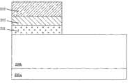
为了解决上述问题,现在已经提出了凹陷沟道型PNPN场效应晶体管,其结构如图1所示,它是沿该器件沟道长度方向的截面图。所述的凹陷沟道型PNPN场效应晶体管包括一个栅叠层区,一个源区、一个漏区和一个衬底区。栅叠层区由栅氧化层104、高K材料层105以及导体层106组成,导体层106采用金属栅材料或者掺杂的多晶硅材料。栅叠层区的侧墙107为绝缘介质比如为Si3N4材料,侧墙107将栅区导体层106与该器件的其它导体层隔离。源区103的掺杂类型通常与漏区101和耗尽区102的掺杂类型相反,并与衬底100c的掺杂类型相同。源区103和漏区101之间贴近栅氧化层104的衬底表面为器件的电流沟道区域。衬底100a和100b为含轻掺杂第一种或第二种杂质的硅层,或为绝缘氧化层。绝缘层108为该晶体管的钝化层,它将所述晶体管与其它器件隔开。导体109、110和111为金属铝或者金属钨,分别为该晶体管源极、栅极和漏极的电极。凹陷型的沟道结构使得晶体管在减小漏电流的同时增大了驱动电流,也就是在降低芯片功耗的同时提高了芯片的性能。在目前的凹陷沟道型PNPN场效应晶体管的制造工艺中,通常是先通过离子注入工艺形成漏区,并通过连续的两次外延工艺或者两次离子注入工艺形成源区和耗尽区,以图1所提供凹陷沟道型PNPN场效应晶体管为例,其详细步骤为:In order to solve the above problems, a recessed channel type PNPN field effect transistor has been proposed, and its structure is shown in Figure 1, which is a cross-sectional view along the channel length of the device. The recessed channel type PNPN field effect transistor includes a gate stack region, a source region, a drain region and a substrate region. The gate stack region is composed of a gate oxide layer 104 , a high-K material layer 105 and a conductor layer 106 , and the conductor layer 106 is made of metal gate material or doped polysilicon material. The sidewall 107 of the gate stack region is an insulating medium such as Si3 N4 material, and the sidewall 107 isolates the conductor layer 106 of the gate region from other conductor layers of the device. The doping type of the source region 103 is generally opposite to that of the drain region 101 and the depletion region 102 and the same as that of the substrate 100c. The substrate surface close to the gate oxide layer 104 between the source region 103 and the drain region 101 is the current channel region of the device. The substrates 100a and 100b are silicon layers lightly doped with the first or second impurity, or insulating oxide layers. The insulating layer 108 is a passivation layer for the transistor, which isolates the transistor from other devices. The conductors 109, 110 and 111 are metal aluminum or metal tungsten, and are respectively the electrodes of the source, gate and drain of the transistor. The recessed channel structure enables the transistor to increase the driving current while reducing the leakage current, that is, to improve the performance of the chip while reducing the power consumption of the chip. In the current manufacturing process of the recessed channel type PNPN field effect transistor, the drain region is usually formed by the ion implantation process first, and the source region and the depletion region are formed by two consecutive epitaxial processes or two ion implantation processes, so that The recessed channel type PNPN field effect transistor provided in Figure 1 is taken as an example, and the detailed steps are as follows:
提供一个包含衬底100a、100b和100c的半导体衬底;providing a semiconductor substrate comprising substrates 100a, 100b and 100c;
通过离子注入形成第二种掺杂类型的漏区101;Forming the drain region 101 of the second doping type by ion implantation;
淀积形成一层硬质掩膜,比如为氮化硅薄膜;Deposit to form a hard mask, such as silicon nitride film;
对所述硬质掩膜和半导体衬底进行刻蚀形成器件的凹陷沟道区域;Etching the hard mask and the semiconductor substrate to form a recessed channel region of the device;
剥除剩余的硬质掩膜;Strip the remaining hard mask;
依次形成一层栅氧化层104、一层高K材料层105和一层导电层106;sequentially forming a gate oxide layer 104, a high-K material layer 105 and a conductive layer 106;
刻蚀形成器件的栅极结构;Etching to form the gate structure of the device;
淀积形成第一种绝缘薄膜;Depositing and forming a first insulating film;
对所述第一层绝缘薄膜、高K材料层和半导体衬底进行刻蚀以形成用于形成源区的区域;Etching the first insulating film, the high-K material layer and the semiconductor substrate to form a region for forming a source region;
外延形成具有第二种掺杂类型的耗尽区102;Epitaxially forming a depletion region 102 with the second doping type;
外延形成具有第一种掺杂类型的源区103;Epitaxially forming the source region 103 with the first doping type;
刻蚀第一种绝缘薄膜形成栅极侧墙107;Etching the first insulating film to form gate spacers 107;
刻蚀高K材料层105露出漏区101;Etching the high-K material layer 105 to expose the drain region 101;
淀积形成第二种绝缘薄膜108,并对其进行刻蚀形成通孔结构;Depositing and forming a second insulating film 108, and etching it to form a through-hole structure;
淀积第一种导电薄膜形成源极电极109、栅极电极110和漏极电极111。The first conductive film is deposited to form the source electrode 109 , the gate electrode 110 and the drain electrode 111 .
如上所述,传统的凹陷沟道型PNPN场效应晶体管的制造工艺中,是先通过离子注入工艺形成漏区,然后刻蚀形成凹陷沟道区域,再在凹陷沟道区域的非漏区侧通过两次外延工艺或者两次离子注入工艺形成源区和耗尽区,其工艺过程复杂,生产成本高。As mentioned above, in the traditional manufacturing process of the recessed channel type PNPN field effect transistor, the drain region is first formed by the ion implantation process, and then the recessed channel region is formed by etching, and then passed through the non-drain region side of the recessed channel region. The source region and the depletion region are formed by two epitaxial processes or two ion implantation processes, and the process is complicated and the production cost is high.
发明内容Contents of the invention
本发明的目的在于提出一种凹陷沟道型PNPN场效应晶体管的制造方法,该方法可以简化传统凹陷沟道型PNPN场效应晶体管的制造工艺,降低生产成本。The object of the present invention is to provide a method for manufacturing a recessed channel type PNPN field effect transistor, which can simplify the manufacturing process of the traditional recessed channel type PNPN field effect transistor and reduce production costs.
本发明提出的凹陷沟道型PNPN场效应晶体管的制造方法,具体步骤如下:The manufacturing method of the recessed channel type PNPN field effect transistor that the present invention proposes, concrete steps are as follows:
提供一个具有第一种掺杂类型的半导体衬底;providing a semiconductor substrate having a first doping type;
进行离子注入,在提供的半导体衬底内形成第一种掺杂类型的区域;performing ion implantation to form regions of the first doping type within the provided semiconductor substrate;
淀积形成第一种绝缘薄膜;Depositing and forming a first insulating film;
刻蚀部分所述第一种绝缘薄膜和第一种掺杂类型的区域,露出进行后续掺杂的半导体衬底区域;Etching part of the first insulating film and the first doping type region to expose the semiconductor substrate region for subsequent doping;
淀积形成第二种绝缘掩膜,并对所述第二种绝缘薄膜进行刻蚀形成侧墙;depositing to form a second type of insulating mask, and etching the second type of insulating film to form sidewalls;
在提供的半导体衬底内,通过扩散工艺形成第二种掺杂类型的区域;In the provided semiconductor substrate, a region of the second doping type is formed by a diffusion process;
淀积形成第三种绝缘掩膜;Depositing and forming a third insulating mask;
刻蚀形成器件的凹陷沟道区域;Etching to form a recessed channel region of the device;
形成第四种绝缘薄膜;Form the fourth insulating film;
淀积形成第一种导电薄膜;Depositing and forming the first conductive film;
刻蚀形成器件的栅极结构;Etching to form the gate structure of the device;
剥除剩余的第一种、第三种绝缘薄膜;Peel off the remaining first and third insulating films;
淀积形成第五种绝缘薄膜,并对所述第五种绝缘薄膜进行刻蚀形成通孔结构;Depositing and forming a fifth insulating film, and etching the fifth insulating film to form a through-hole structure;
淀积第二种导电薄膜形成电极。A second conductive film is deposited to form electrodes.
所述半导体衬底为单晶硅、多晶硅或者绝缘体上的硅(SOI)。所述第一种、第二种、第三种、第五种绝缘薄膜可为二氧化硅、氮化硅或者为它们之间相混合的绝缘材料。所述第四种绝缘薄膜可为SiO2、HfO2、HfSiO、HfSiON、SiON或Al2O3,或者为它们之中几种的混合物。所述第一种导电薄膜可为TiN、TaN、RuO2、Ru或WSi合金,或者为其掺杂的多晶硅材料。所述的第二种导电薄膜为金属铝、金属钨或者为其它金属导电材料。The semiconductor substrate is single crystal silicon, polycrystalline silicon or silicon on insulator (SOI). The first, second, third and fifth insulating films can be silicon dioxide, silicon nitride or insulating materials mixed therebetween. The fourth insulating film can be SiO2 , HfO2 , HfSiO, HfSiON, SiON or Al2 O3 , or a mixture of several of them. The first conductive thin film can be TiN, TaN, RuO2 , Ru or WSi alloy, or its doped polysilicon material. The second conductive film is metal aluminum, metal tungsten or other metal conductive materials.
进一步地,所述的第一种掺杂类型为n型,第二种掺杂类型p型;或者,所述的第一种掺杂类型为p型,第二种掺杂类型n型。Further, the first doping type is n-type, and the second doping type is p-type; or, the first doping type is p-type, and the second doping type is n-type.
更进一步地,所述凹陷沟道区域形成前,所述第二种掺杂类型的区域在水平方向上延伸至所述第一种掺杂类型的区域下方。所述凹陷沟道区域将所述第二种掺杂类型的区域分隔为两个部分,并且,被分割的两个部分中的一部分位于所述第一种掺杂类型的区域下方。Furthermore, before the recessed channel region is formed, the region of the second doping type extends below the region of the first doping type in the horizontal direction. The recessed channel region divides the region of the second doping type into two parts, and a part of the two divided parts is located below the region of the first doping type.
本发明提出的凹陷沟道型PNPN场效应晶体管的制造方法,是通过自对准工艺形成源区、耗尽区和漏区,只需要进行一次离子注入工艺和一次扩散工艺,工艺过程简单,效率高,降低了生产成本。The manufacturing method of the recessed channel type PNPN field effect transistor proposed by the present invention is to form a source region, a depletion region and a drain region through a self-alignment process, and only needs to perform an ion implantation process and a diffusion process, and the process is simple and efficient. High, reducing production costs.
附图说明Description of drawings
图1为现有的一种凹陷沟道型PNPN场效应晶体管结构的截面图。FIG. 1 is a cross-sectional view of a conventional recessed channel type PNPN field effect transistor structure.
图2a至图2g为本发明提供的凹陷沟道型PNPN场效应晶体管的制造方法的一个实施例工艺流程图。2a to 2g are process flow charts of an embodiment of the manufacturing method of the recessed channel type PNPN field effect transistor provided by the present invention.
具体实施方式Detailed ways
下面将参照附图对本发明的一个示例性实施方式作详细说明。在图中,为了方便说明,放大了层和区域的厚度,所示大小并不代表实际尺寸。尽管这些图并不是完全准确的反映出器件的实际尺寸,但是它们还是完整的反映了区域和组成结构之间的相互位置,特别是组成结构之间的上下和相邻关系。An exemplary embodiment of the present invention will be described in detail below with reference to the accompanying drawings. In the drawings, the thicknesses of layers and regions are exaggerated for convenience of illustration, and the shown sizes do not represent actual sizes. Although these figures do not completely reflect the actual size of the device, they still fully reflect the mutual positions between the regions and the constituent structures, especially the upper-lower and adjacent relationships between the constituent structures.
参考图是本发明的理想化实施例的示意图,本发明所示的实施例不应该被认为仅限于图中所示区域的特定形状,而是包括所得到的形状,比如制造引起的偏差。例如刻蚀得到的曲线通常具有弯曲或圆润的特点,但在本发明实施例中,均以矩形表示,图中的表示是示意性的,但这不应该被认为是限制本发明的范围。同时在下面的描述中,所使用的术语衬底可以理解为包括正在工艺加工中的半导体衬底,可能包括在其上所制备的其它薄膜层。The referenced figures are schematic illustrations of idealized embodiments of the invention, and the illustrated embodiments of the invention should not be construed as limited to the particular shapes of regions illustrated in the figures but are to include resulting shapes, such as manufacturing-induced deviations. For example, the curves obtained by etching are usually curved or rounded, but in the embodiment of the present invention, they are all represented by rectangles. The representation in the figure is schematic, but this should not be considered as limiting the scope of the present invention. Meanwhile, in the following description, the term substrate used can be understood to include the semiconductor substrate being processed, possibly including other thin film layers prepared thereon.
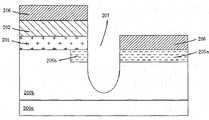
首先,在提供的半导体衬底上进行p型离子注入形成掺杂区201a,如图2a所示,其中,衬底200a为含轻掺杂n型或者p型杂质的硅层,或为绝缘氧化层;衬底200b为轻掺杂p型杂质的硅层。First, perform p-type ion implantation on the provided semiconductor substrate to form a doped
接下来,淀积形成一层绝缘薄膜202和一层光刻胶203,然后刻蚀绝缘薄膜202和掺杂区201a,形成源区201并露出进行后续掺杂的半导体衬底区域,如图2b所示。绝缘薄膜202可以为二氧化硅、氮化硅或者为它们之间相混合的绝缘材料。Next, deposit and form a layer of insulating
接下来,淀积形成一层氮化硅薄膜,并对氮化硅薄膜进行刻蚀形成源区201的侧墙204,如图2c所示。Next, deposit and form a silicon nitride film, and etch the silicon nitride film to form sidewalls 204 of the
接下来,利用扩散工艺,形成n型扩散区205,如图2d所示,n型扩散区205延伸至源区201的下方。Next, an n-
接下来,淀积形成一层绝缘薄膜206比如为二氧化硅或者氮化硅,然后刻蚀形成器件的凹陷沟道区域207,在此步工艺中,侧墙204被完全刻蚀掉,n型扩散区205也会被部分刻蚀掉并且被凹陷沟道区域207分隔成为漏区205a和耗尽区205b,如图2e所示。同时还需要注意的是,在此步工艺中,源区201可以不被刻蚀,也可以被部分刻蚀掉。Next, deposit and form a layer of insulating
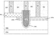
接下来,形成一层绝缘薄膜208,绝缘薄膜208包括一层热生长的二氧化硅薄膜和一层高k材料层。再淀积形成一层导电薄膜209,导电薄膜209可以为TiN、TaN、RuO2、Ru、WSi合金或者为掺杂的多晶硅材料,然后刻蚀形成器件的栅极结构,如图2f所示。绝缘薄膜208中,二氧化硅作为绝缘层,厚度为几个埃,目的是改善界面特性;高K材料层的厚度为几个纳米到十几个纳米,目的是减小漏电流。Next, an insulating
最后,刻蚀掉多余的绝缘薄膜208,并剥除剩余的绝缘薄膜206和绝缘薄膜202,接着,淀积形成一层绝缘薄膜210,然后对绝缘薄膜210进行刻蚀形成通孔结构,绝缘薄膜210可以为氧化硅或为氮化硅,接着再淀积一层金属,可以为铝或为钨。然后刻蚀形成源极电极211、栅极电极212和漏极电极213,最终形成如图2g所示的凹陷沟道PNPN场效应晶体管。Finally, the redundant insulating
如上所述,在不偏离本发明精神和范围的情况下,还可以构成许多有很大差别的实施例。应当理解,除了如所附的权利要求所限定的,本发明不限于在说明书中所述的具体实例。As mentioned above, many widely different embodiments can be constructed without departing from the spirit and scope of the present invention. It should be understood that the invention is not limited to the specific examples described in the specification, except as defined in the appended claims.
Claims (9)
Translated fromChinesePriority Applications (1)
| Application Number | Priority Date | Filing Date | Title |
|---|---|---|---|
| CN2010101863734ACN101866858B (en) | 2010-05-27 | 2010-05-27 | Manufacture method of sinking channel type PNPN field effect transistor |
Applications Claiming Priority (1)
| Application Number | Priority Date | Filing Date | Title |
|---|---|---|---|
| CN2010101863734ACN101866858B (en) | 2010-05-27 | 2010-05-27 | Manufacture method of sinking channel type PNPN field effect transistor |
Publications (2)
| Publication Number | Publication Date |
|---|---|
| CN101866858A CN101866858A (en) | 2010-10-20 |
| CN101866858Btrue CN101866858B (en) | 2012-07-04 |
Family
ID=42958507
Family Applications (1)
| Application Number | Title | Priority Date | Filing Date |
|---|---|---|---|
| CN2010101863734AExpired - Fee RelatedCN101866858B (en) | 2010-05-27 | 2010-05-27 | Manufacture method of sinking channel type PNPN field effect transistor |
Country Status (1)
| Country | Link |
|---|---|
| CN (1) | CN101866858B (en) |
Families Citing this family (2)
| Publication number | Priority date | Publication date | Assignee | Title |
|---|---|---|---|---|
| KR101620532B1 (en)* | 2010-12-17 | 2016-05-12 | 킹스톤 세미컨덕터 코.,엘티디. | Doping method, pn structure, method for fabricating solar cell, and solar cell |
| CN103413829B (en)* | 2013-08-06 | 2018-04-27 | 复旦大学 | One kind is U-shaped to enclose grid tunneling transistor device and its manufacture method |
Citations (3)
| Publication number | Priority date | Publication date | Assignee | Title |
|---|---|---|---|---|
| CN1726596A (en)* | 2002-12-12 | 2006-01-25 | 西利康尼克斯股份有限公司 | Trench metal oxide semiconductor field effect transistor with implanted drain drift region and method of manufacturing the same |
| US7465976B2 (en)* | 2005-05-13 | 2008-12-16 | Intel Corporation | Tunneling field effect transistor using angled implants for forming asymmetric source/drain regions |
| CN101699617A (en)* | 2009-10-29 | 2010-04-28 | 复旦大学 | Preparation method of self-aligned tunneling field effect transistor |
Family Cites Families (1)
| Publication number | Priority date | Publication date | Assignee | Title |
|---|---|---|---|---|
| US7880160B2 (en)* | 2006-05-22 | 2011-02-01 | Qimonda Ag | Memory using tunneling field effect transistors |
- 2010
- 2010-05-27CNCN2010101863734Apatent/CN101866858B/ennot_activeExpired - Fee Related
Patent Citations (3)
| Publication number | Priority date | Publication date | Assignee | Title |
|---|---|---|---|---|
| CN1726596A (en)* | 2002-12-12 | 2006-01-25 | 西利康尼克斯股份有限公司 | Trench metal oxide semiconductor field effect transistor with implanted drain drift region and method of manufacturing the same |
| US7465976B2 (en)* | 2005-05-13 | 2008-12-16 | Intel Corporation | Tunneling field effect transistor using angled implants for forming asymmetric source/drain regions |
| CN101699617A (en)* | 2009-10-29 | 2010-04-28 | 复旦大学 | Preparation method of self-aligned tunneling field effect transistor |
Also Published As
| Publication number | Publication date |
|---|---|
| CN101866858A (en) | 2010-10-20 |
Similar Documents
| Publication | Publication Date | Title |
|---|---|---|
| US7241653B2 (en) | Nonplanar device with stress incorporation layer and method of fabrication | |
| CN110189997B (en) | Stacked nanosheet gate-all-around transistor and preparation method thereof | |
| CN102668093B (en) | Contact with the circulating type of three gated devices for fin FETs | |
| US10964593B2 (en) | Method for forming a semiconductor structure with a gate contact plug | |
| US11462628B2 (en) | Semiconductor device, and manufacturing method thereof | |
| CN101819975B (en) | Vertical channel dual-grate tunneling transistor and preparation method thereof | |
| CN1577850A (en) | Nonplanar semiconductor device with partially or fully wrapped around gate electrode and methods of fabrication | |
| CN105118855A (en) | Semiconductor elements with gate dielectrics of various thicknesses | |
| US20120261744A1 (en) | Microelectronic device structure and manufacturing method thereof | |
| CN115346922A (en) | Integrated circuits and methods of forming them | |
| CN102437060B (en) | Method for producing tunneling field effect transistor of U-shaped channel | |
| CN115332309A (en) | Dual silicon-on-insulator device and method of making the same | |
| WO2022048163A1 (en) | Laterally-diffused metal-oxide semiconductor apparatus and preparation method therefor, and electronic device | |
| CN110957370B (en) | Method for manufacturing lateral double-diffused transistor | |
| TW202333381A (en) | Method of manufacturing a semiconductor device and a semiconductor device | |
| CN101834210A (en) | A kind of PNPN field effect transistor with recessed channel and its preparation method | |
| US11387317B2 (en) | Field-effect transistor without punch-through stopper and fabrication method thereof | |
| CN101866858B (en) | Manufacture method of sinking channel type PNPN field effect transistor | |
| CN111162074B (en) | Semiconductor structure and method of forming the same | |
| US12389633B2 (en) | Source/drains in semiconductor devices and methods of forming thereof | |
| US8586432B2 (en) | Method for manufacturing vertical-channel tunneling transistor | |
| CN108022926B (en) | Semiconductor device and method of forming the same | |
| CN110828542A (en) | Semiconductor device and forming method thereof | |
| CN101814503B (en) | Complementary grid-controlled PNPN field effect transistor and preparation method thereof | |
| CN101807601A (en) | Grid-control PNPN field-effect transistor by utilizing SiGe source electrode and preparation method thereof |
Legal Events
| Date | Code | Title | Description |
|---|---|---|---|
| C06 | Publication | ||
| PB01 | Publication | ||
| C10 | Entry into substantive examination | ||
| SE01 | Entry into force of request for substantive examination | ||
| C14 | Grant of patent or utility model | ||
| GR01 | Patent grant | ||
| CF01 | Termination of patent right due to non-payment of annual fee | Granted publication date:20120704 Termination date:20190527 | |
| CF01 | Termination of patent right due to non-payment of annual fee |