CN101852934A - Touch type liquid crystal display screen - Google Patents
Touch type liquid crystal display screenDownload PDFInfo
- Publication number
- CN101852934A CN101852934ACN201010187834ACN201010187834ACN101852934ACN 101852934 ACN101852934 ACN 101852934ACN 201010187834 ACN201010187834 ACN 201010187834ACN 201010187834 ACN201010187834 ACN 201010187834ACN 101852934 ACN101852934 ACN 101852934A
- Authority
- CN
- China
- Prior art keywords
- layer
- carbon nanotube
- transparency conducting
- tube
- carbon nano
- Prior art date
- Legal status (The legal status is an assumption and is not a legal conclusion. Google has not performed a legal analysis and makes no representation as to the accuracy of the status listed.)
- Pending
Links
Images


Classifications
- G—PHYSICS
- G06—COMPUTING OR CALCULATING; COUNTING
- G06F—ELECTRIC DIGITAL DATA PROCESSING
- G06F3/00—Input arrangements for transferring data to be processed into a form capable of being handled by the computer; Output arrangements for transferring data from processing unit to output unit, e.g. interface arrangements
- G06F3/01—Input arrangements or combined input and output arrangements for interaction between user and computer
- G06F3/03—Arrangements for converting the position or the displacement of a member into a coded form
- G06F3/041—Digitisers, e.g. for touch screens or touch pads, characterised by the transducing means
- G06F3/0412—Digitisers structurally integrated in a display
- G—PHYSICS
- G06—COMPUTING OR CALCULATING; COUNTING
- G06F—ELECTRIC DIGITAL DATA PROCESSING
- G06F3/00—Input arrangements for transferring data to be processed into a form capable of being handled by the computer; Output arrangements for transferring data from processing unit to output unit, e.g. interface arrangements
- G06F3/01—Input arrangements or combined input and output arrangements for interaction between user and computer
- G06F3/03—Arrangements for converting the position or the displacement of a member into a coded form
- G06F3/041—Digitisers, e.g. for touch screens or touch pads, characterised by the transducing means
- G06F3/044—Digitisers, e.g. for touch screens or touch pads, characterised by the transducing means by capacitive means
- G06F3/0443—Digitisers, e.g. for touch screens or touch pads, characterised by the transducing means by capacitive means using a single layer of sensing electrodes
- G—PHYSICS
- G06—COMPUTING OR CALCULATING; COUNTING
- G06F—ELECTRIC DIGITAL DATA PROCESSING
- G06F3/00—Input arrangements for transferring data to be processed into a form capable of being handled by the computer; Output arrangements for transferring data from processing unit to output unit, e.g. interface arrangements
- G06F3/01—Input arrangements or combined input and output arrangements for interaction between user and computer
- G06F3/03—Arrangements for converting the position or the displacement of a member into a coded form
- G06F3/041—Digitisers, e.g. for touch screens or touch pads, characterised by the transducing means
- G06F3/044—Digitisers, e.g. for touch screens or touch pads, characterised by the transducing means by capacitive means
- G06F3/0446—Digitisers, e.g. for touch screens or touch pads, characterised by the transducing means by capacitive means using a grid-like structure of electrodes in at least two directions, e.g. using row and column electrodes
Landscapes
- Engineering & Computer Science (AREA)
- General Engineering & Computer Science (AREA)
- Theoretical Computer Science (AREA)
- Human Computer Interaction (AREA)
- Physics & Mathematics (AREA)
- General Physics & Mathematics (AREA)
- Liquid Crystal (AREA)
- Position Input By Displaying (AREA)
- Carbon And Carbon Compounds (AREA)
Abstract
Description
Translated fromChinese技术领域technical field
本发明涉及一种液晶显示屏,尤其涉及一种触摸式液晶显示屏。The invention relates to a liquid crystal display screen, in particular to a touch type liquid crystal display screen.
背景技术Background technique
液晶显示因为低功耗、小型化及高质量的显示效果,成为最佳的显示方式之一。近年来,伴随着移动电话、触摸导航系统、集成式电脑显示器及互动电视等各种电子设备的高性能化和多样化的发展,在液晶显示屏的显示面安装透光性的触摸屏的电子设备逐渐增加。电子设备的使用者通过触摸屏,一边对位于触摸屏背面的液晶显示屏的显示内容进行视觉确认,一边利用手指或笔等方式按压触摸屏来进行操作。由此,可以操作使用该液晶显示屏的电子设备的各种功能。Liquid crystal display has become one of the best display methods because of low power consumption, miniaturization and high-quality display effect. In recent years, with the high-performance and diversified development of various electronic devices such as mobile phones, touch navigation systems, integrated computer monitors, and interactive TVs, electronic devices that install light-transmitting touch screens on the display surface of liquid crystal displays gradually increase. The user of the electronic device uses the touch screen to visually confirm the display content of the liquid crystal display located on the back of the touch screen, and at the same time presses the touch screen with a finger or a pen to perform operations. Thereby, various functions of electronic equipment using the liquid crystal display can be operated.
然而,现有的使用电容触摸屏的液晶显示屏从外至内依次包括一电容触摸屏、一第一偏光片、一第二基体、一第一配向层、液晶层、一第二配向层、一薄膜晶体管模板以及一第二偏光片。所述电容触摸屏可以为单点式或多点式,以多点电容触摸屏常用投射式电容触摸屏为例,其从外至内一般包括一第一基体、一第一铟锡氧化物(Indium Tin Oxide,ITO)层(下称ITO层)、一第二基体、一第二ITO层,该第二ITO层与所述第一偏光片接触设置。由此可见,将触摸屏集成在液晶显示屏中必然使得液晶显示屏的厚度增加,结构比较复杂,不利于液晶显示屏及应用液晶显示屏的电子设备的小型化和薄型化的发展。However, an existing liquid crystal display using a capacitive touch screen sequentially includes a capacitive touch screen, a first polarizer, a second substrate, a first alignment layer, a liquid crystal layer, a second alignment layer, and a thin film from outside to inside. Transistor template and a second polarizer. The capacitive touch screen can be single-point or multi-point. Taking the projected capacitive touch screen commonly used in multi-point capacitive touch screens as an example, it generally includes a first substrate, a first Indium Tin Oxide (Indium Tin Oxide) from the outside to the inside. , ITO) layer (hereinafter referred to as ITO layer), a second substrate, a second ITO layer, the second ITO layer is arranged in contact with the first polarizer. It can be seen that integrating the touch screen into the liquid crystal display will inevitably increase the thickness of the liquid crystal display and complicate the structure, which is not conducive to the development of miniaturization and thinning of the liquid crystal display and electronic equipment using the liquid crystal display.
有鉴于此,确有必要提供一种触摸式液晶屏,该触摸式液晶屏具有较薄的厚度,结构更简单。In view of this, it is indeed necessary to provide a touch-type liquid crystal screen, which has a thinner thickness and a simpler structure.
发明内容Contents of the invention
有鉴于此,确有必要提供一种具有比较薄的厚度,结构比较简单的触摸式液晶显示屏。In view of this, it is indeed necessary to provide a touch-type LCD with a relatively thin thickness and a relatively simple structure.
一种触摸式液晶显示屏从上至下依次包括:一电容式触摸屏,该电容式触摸屏包括一第一基体及一透明导电层,该透明导电层设置于该第一基体的上表面,该透明导电层为导电异向性层,该导电异向性层为一碳纳米管层,该碳纳米管层包括多个碳纳米管,且该碳纳米管层中的碳纳米管沿同一方向择优取向延伸;一上基板,该上基板从上至下依次包括一第一偏光片、一上基体、一上电极以及一第一配向层,其中,所述第一偏光片为所述碳纳米管层,所述上基体为所述第一基体;一液晶层;以及一下基板,该下基板从上至下依次包括一第二配向层、一薄膜晶体管面板以及一第二偏光片。A touch-type liquid crystal display screen includes from top to bottom: a capacitive touch screen, the capacitive touch screen includes a first substrate and a transparent conductive layer, the transparent conductive layer is arranged on the upper surface of the first substrate, the transparent The conductive layer is a conductive anisotropic layer, the conductive anisotropic layer is a carbon nanotube layer, the carbon nanotube layer includes a plurality of carbon nanotubes, and the carbon nanotubes in the carbon nanotube layer are preferentially oriented in the same direction Extension; an upper substrate, the upper substrate sequentially includes a first polarizer, an upper substrate, an upper electrode and a first alignment layer from top to bottom, wherein the first polarizer is the carbon nanotube layer , the upper substrate is the first substrate; a liquid crystal layer; and a lower substrate, the lower substrate sequentially includes a second alignment layer, a thin film transistor panel and a second polarizer from top to bottom.
一种触摸式液晶显示屏从上至下依次包括:一电容式触摸屏,该电容式触摸屏从上至下依次包括:一第二透明导电层、一第二基体、一第一透明导电层以及一第一基体;一上基板,该上基板从上至下依次包括一第一偏光片、一上基体、一上电极以及一第一配向层;一液晶层;以及一下基板,该下基板从上至下依次包括一第二配向层、一薄膜晶体管面板以及一第二偏光片;其中,所述第一透明导电层与第二透明导电层中的一个透明导电层为导电异向性层,该导电各向异性层为一碳纳米管层,该碳纳米管层包括多个碳纳米管,且该碳纳米管层中的碳纳米管沿同一方向择优取向延伸,另一个透明导电层包括多个间隔设置的导电结构,所述第一偏光片为所述碳纳米管层,所述上基体为所述第一基体。A touch-type liquid crystal display screen includes: a capacitive touch screen from top to bottom, and the capacitive touch screen includes: a second transparent conductive layer, a second substrate, a first transparent conductive layer and a The first substrate; an upper substrate, the upper substrate sequentially includes a first polarizer, an upper substrate, an upper electrode and a first alignment layer from top to bottom; a liquid crystal layer; and a lower substrate, the lower substrate from the upper including a second alignment layer, a thin film transistor panel, and a second polarizer in sequence; wherein, one of the first transparent conductive layer and the second transparent conductive layer is a conductive anisotropic layer, the The conductive anisotropic layer is a carbon nanotube layer, the carbon nanotube layer includes a plurality of carbon nanotubes, and the carbon nanotubes in the carbon nanotube layer extend along the same direction, and the other transparent conductive layer includes a plurality of Conductive structures arranged at intervals, the first polarizer is the carbon nanotube layer, and the upper substrate is the first substrate.
与现有技术相比较,本发明提供的触摸式液晶显示屏采用碳纳米管层不仅作为触摸屏的透明导电层,而且兼作该触摸式液晶显示屏的第一偏光片,所述电容式触摸屏中的第一基体兼作所述上基板的上基体,因此,该触摸式液晶显示屏具有简单的结构和较薄的厚度,简化了制造工艺,降低了制造成本。Compared with the prior art, the touch-type liquid crystal display provided by the present invention adopts the carbon nanotube layer not only as the transparent conductive layer of the touch-screen, but also as the first polarizer of the touch-type liquid crystal display. The first substrate doubles as the upper substrate of the upper substrate. Therefore, the touch-type liquid crystal display has a simple structure and a relatively thin thickness, which simplifies the manufacturing process and reduces the manufacturing cost.
附图说明Description of drawings
图1是本发明第一实施例提供的触摸式液晶显示屏的剖面示意图。FIG. 1 is a schematic cross-sectional view of a touch-type liquid crystal display provided by a first embodiment of the present invention.
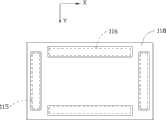
图2是图1中的触摸屏的俯视示意图。FIG. 2 is a schematic top view of the touch screen in FIG. 1 .
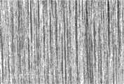
图3是图1中的透明导电层采用的碳纳米管拉膜的扫描电镜照片。Fig. 3 is a scanning electron micrograph of the carbon nanotube drawn film used in the transparent conductive layer in Fig. 1 .
图4是本发明第二实施例提供的触摸式液晶显示屏的剖面示意图。FIG. 4 is a schematic cross-sectional view of a touch-type liquid crystal display provided by a second embodiment of the present invention.
图5是图4中的触摸屏的俯视示意图。FIG. 5 is a schematic top view of the touch screen in FIG. 4 .
主要元件符号说明Description of main component symbols
触摸式液晶显示屏 10;20Touch
触摸屏 110;210
第一基体 112;211
透明导电层 114Transparent
第一电极 115;216
第二电极 116;218
透明保护层 118;215Transparent
上基板 120;220
第一配向层 122;222
上电极 124;224
下基板 130;230
第二配向层 132;232
薄膜晶体管面板 134;234Thin
第二偏光片 136;236
液晶层 140;240
第一透明导电层 212The first transparent
第二基体 213
第二透明导电层 214The second transparent
具体实施方式Detailed ways
下面将结合附图及具体实施例,对本发明提供的触摸式液晶显示屏作进一步的详细说明。The touch-type liquid crystal display screen provided by the present invention will be further described in detail below in conjunction with the accompanying drawings and specific embodiments.
请参阅图1,本发明第一实施例提供一种触摸式液晶显示屏10。该触摸式液晶显示屏10其包括:一触摸屏110、一上基板120、一下基板130及一液晶层140。其中,所述触摸屏110设置于该上基板120的上表面;所述下基板130与所述上基板120相对设置;所述液晶层140设置于所述上基板120与所述下基板130之间。在本说明书中,“上”、“下”仅指相对的方位,“上”是指靠近触摸式液晶显示屏的触摸表面的方向,而“下”则指远离触摸式液晶显示屏的触摸表面的方向。Referring to FIG. 1 , the first embodiment of the present invention provides a touch-type
请一并参阅图2,所述触摸屏110为一表面电容式触摸屏,该触摸屏110包括一第一基体112、一透明导电层114、两个第一电极115、两个第二电极116以及一透明保护层118。其中,所述透明导电层114设置于所述第一基体112的上表面;所述两个第一电极115以及两个第二电极116与所述透明导电层114电连接;所述透明保护层118可直接设置在所述透明导电层114的上表面,用于保护该透明导电层114。Please also refer to FIG. 2, the
所述上基板120从上至下依次包括一透明导电层114、一第一基体112、一上电极124及一第一配向层122。其中,所述上电极124设置于所述第一基体112的下表面。所述第一配向层122设置于所述上电极124的下表面,靠近液晶层140设置。进一步地,该第一配向层122的下表面可包括多个平行的第一沟槽,用于使液晶层140的液晶分子定向排列。The
其中,所述触摸屏110中的透明导电层114还兼作所述上基板120的第一偏光片,所述第一基体112既作为所述触摸屏110的基体,又作为所述上基板120的上基体,因此,所述触摸式液晶显示屏10具有较薄的厚度和简单的结构,简化了制造工艺,降低了制造成本,提高了背光源的利用率,改善了显示质量。Wherein, the transparent
所述液晶层140包括多个长棒状的液晶分子。所述液晶层140的液晶材料为现有技术中常用的液晶材料。所述液晶层140的厚度1~50微米,本实施例中,液晶层140的厚度为5微米。The
所述下基板130从上至下依次包括一第二配向层132、一薄膜晶体管面板134及一第二偏光片136。该第二配向层132设置在该薄膜晶体管面板134的上表面,靠近所述液晶层140设置。进一步地,第二配向层132的上表面可包括多个平行的第二沟槽,该第二沟槽的排列方向与所述第一配向层122的第一沟槽的排列方向垂直。该第二偏光片136设置在该薄膜晶体管面板134的下表面。The
可以理解,根据各种功能的需求,上述各层之间还可选择性地插入额外的其他层。It can be understood that, according to the requirements of various functions, additional layers can also be selectively inserted between the above layers.
所述第一基体112为透明的薄膜或薄板。该第一基体112的材料可以为玻璃、石英或金刚石等硬性材料。所述第一基体112主要起支撑的作用。当用于柔性触摸屏中时,该第一基体112的材料也可为塑料或树脂等柔性材料。具体地,该第一基体112所用的材料可以为聚碳酸酯(PC)、聚甲基丙烯酸甲酯(PMMA)、聚对苯二甲酸乙二醇酯(PET)等聚酯材料,或聚醚砜(PES)、纤维素酯、聚氯乙烯(PVC)、苯并环丁烯(BCB)或丙烯酸树脂等材料。该第一基体112的厚度为1毫米~1厘米。本实施例中,该第一基体112的材料为玻璃,厚度均为5毫米。可以理解,形成第一基体112的材料并不限于上述列举的材料,只要能使所述第一基体112具有较好的透明度,起到支撑的作用即可。The
所述触摸屏110中的透明导电层114为一碳纳米管层。碳纳米管层为一电阻异向性层。所述碳纳米管层包括多个碳纳米管,且该多个碳纳米管沿同一方向择优取向排列,从而使得碳纳米管层在一在方向的电阻小于其他方向的电阻。该碳纳米管层中大多数碳纳米管的延伸方向基本平行于该碳纳米管层的表面,且在碳纳米管延伸方向上的电阻率小于其他方向上的电阻率,优选地,所述碳纳米管层在碳纳米管延伸方向上的电阻率与其他方向上的电阻率的比值小于等于1∶2,即碳纳米管层在碳纳米管延伸方向上的电导率是其他方向的2倍以上。所述碳纳米管层包括至少一个碳纳米管拉膜。其中,当所述碳纳米管层包括多个碳纳米管拉膜时,该碳纳米管拉膜层叠设置或平行无间隙铺设设置,且该多个碳纳米管拉膜中的大多数碳纳米管基本沿同一方向择优取向排列,即相邻的碳纳米管拉膜中的碳纳米管的排列方向基本一致。本实施例中,所述碳纳米管层为一个碳纳米管拉膜,即所述透明导电层114由一个碳纳米管拉膜组成。所述碳纳米管层的厚度不限,可以根据需要选择;所述碳纳米管层的厚度为0.5纳米~100微米;优选地,该碳纳米管层的厚度为100纳米~200纳米。The transparent
请参阅图3,所述碳纳米管拉膜是由若干碳纳米管组成的自支撑结构。所述若干碳纳米管为沿同一方向择优取向排列。所述择优取向是指在碳纳米管拉膜中大多数碳纳米管的整体延伸方向基本朝同一方向。而且,所述大多数碳纳米管的整体延伸方向基本平行于碳纳米管拉膜的表面。进一步地,所述碳纳米管拉膜中多数碳纳米管是通过范德华力首尾相连。具体地,所述碳纳米管拉膜中基本朝同一方向延伸的大多数碳纳米管中每一碳纳米管与在延伸方向上相邻的碳纳米管通过范德华力首尾相连。当然,所述碳纳米管拉膜中存在少数随机排列的碳纳米管,这些碳纳米管不会对碳纳米管拉膜中大多数碳纳米管的整体取向排列构成明显影响。所述自支撑为碳纳米管拉膜不需要大面积的载体支撑,而只要相对两边提供支撑力即能整体上悬空而保持自身膜状状态,即将该碳纳米管拉膜置于(或固定于)间隔一定距离设置的两个支撑体上时,位于两个支撑体之间的碳纳米管拉膜能够悬空保持自身膜状状态。所述自支撑主要通过碳纳米管拉膜中存在连续的通过范德华力首尾相连延伸排列的碳纳米管而实现。Please refer to FIG. 3 , the carbon nanotube drawn film is a self-supporting structure composed of several carbon nanotubes. The plurality of carbon nanotubes are preferentially aligned along the same direction. The preferred orientation means that the overall extension direction of most carbon nanotubes in the drawn carbon nanotube film basically faces the same direction. Moreover, the overall extension direction of most of the carbon nanotubes is substantially parallel to the surface of the drawn carbon nanotube film. Further, most of the carbon nanotubes in the carbon nanotube drawn film are connected end to end by van der Waals force. Specifically, each carbon nanotube in the majority of carbon nanotubes extending in the same direction in the drawn carbon nanotube film is connected end-to-end with the adjacent carbon nanotubes in the extending direction through van der Waals force. Of course, there are a few randomly arranged carbon nanotubes in the drawn carbon nanotube film, and these carbon nanotubes will not significantly affect the overall alignment of most carbon nanotubes in the drawn carbon nanotube film. The self-supporting carbon nanotube drawn film does not require a large area of carrier support, but as long as the supporting force is provided on both sides, it can be suspended as a whole and maintain its own film state, that is, the carbon nanotube drawn film is placed (or fixed) on ) on two supports arranged at a certain distance, the carbon nanotube stretched film located between the two supports can be suspended in the air to maintain its own film state. The self-supporting is mainly realized by the presence of continuous carbon nanotubes arranged end-to-end by van der Waals force in the carbon nanotube stretched film.
具体地,所述碳纳米管拉膜中基本朝同一方向延伸的多数碳纳米管,并非绝对的直线状,可以适当的弯曲;或者并非完全按照延伸方向上排列,可以适当的偏离延伸方向。因此,不能排除碳纳米管拉膜的基本朝同一方向延伸的多数碳纳米管中并列的碳纳米管之间可能存在部分接触。Specifically, most of the carbon nanotubes extending in the same direction in the drawn carbon nanotube film are not absolutely straight and can be properly bent; or they are not completely arranged in the extending direction and can be appropriately deviated from the extending direction. Therefore, it cannot be ruled out that there may be partial contact between the parallel carbon nanotubes among the carbon nanotubes extending in the same direction in the drawn carbon nanotube film.
具体地,所述碳纳米管拉膜包括多个连续且定向排列的碳纳米管片段。该多个碳纳米管片段通过范德华力首尾相连。每一碳纳米管片段包括多个相互平行的碳纳米管,该多个相互平行的碳纳米管通过范德华力紧密结合。该碳纳米管片段具有任意的长度、厚度、均匀性及形状。该碳纳米管拉膜中的碳纳米管沿同一方向择优取向排列。Specifically, the drawn carbon nanotube film includes a plurality of continuous and aligned carbon nanotube segments. The plurality of carbon nanotube segments are connected end to end by van der Waals force. Each carbon nanotube segment includes a plurality of parallel carbon nanotubes, and the plurality of parallel carbon nanotubes are closely combined by van der Waals force. The carbon nanotube segment has any length, thickness, uniformity and shape. The carbon nanotubes in the carbon nanotube stretched film are preferentially aligned along the same direction.
从碳纳米管阵列中拉取获得所述碳纳米管拉膜的具体方法包括:(a)从所述碳纳米管阵列中选定一碳纳米管片段,本实施例优选为采用具有一定宽度的胶带或粘性基条接触该碳纳米管阵列以选定具有一定宽度的一碳纳米管片段;(b)通过移动该拉伸工具,以一定速度拉取该选定的碳纳米管片段,从而首尾相连的拉出多个碳纳米管片段,进而形成一连续的碳纳米管拉膜。该多个碳纳米管相互并排使该碳纳米管片段具有一定宽度。当该被选定的碳纳米管片段在拉力作用下沿拉取方向逐渐脱离碳纳米管阵列的生长基底的同时,由于范德华力作用,与该选定的碳纳米管片段相邻的其它碳纳米管片段首尾相连地相继地被拉出,从而形成一连续、均匀且具有一定宽度和择优取向的碳纳米管拉膜。The specific method for obtaining the carbon nanotube film by pulling from the carbon nanotube array includes: (a) selecting a carbon nanotube segment from the carbon nanotube array. In this embodiment, a carbon nanotube segment with a certain width is preferably used. Tape or sticky base strip touches this carbon nanotube array to select a carbon nanotube segment with a certain width; (b) pull the selected carbon nanotube segment at a certain speed by moving the stretching tool, thereby end to end A plurality of carbon nanotube segments are pulled out in succession to form a continuous carbon nanotube film. The plurality of carbon nanotubes are arranged side by side so that the carbon nanotube segment has a certain width. When the selected carbon nanotube segment is gradually detached from the growth substrate of the carbon nanotube array along the pulling direction under the action of pulling force, due to the van der Waals force, other carbon nanotubes adjacent to the selected carbon nanotube segment The tube segments are pulled out end to end, thereby forming a continuous, uniform carbon nanotube film with a certain width and preferred orientation.
所述碳纳米管拉膜在拉伸方向具有最小的电阻抗,而在垂直于拉伸方向具有最大电阻抗,因而具备电阻抗异向性,即导电异向性。The carbon nanotube stretched film has the smallest electrical impedance in the stretching direction and the largest electrical impedance in the direction perpendicular to the stretching, so it has electrical impedance anisotropy, that is, electrical conductivity anisotropy.
所述碳纳米管拉膜的结构请参见于2008年8月13日公开的,公开号为CN101239712A的中国发明专利申请公布说明书。由于该碳纳米管拉膜中的碳纳米管具有很好的柔韧性,使得该碳纳米管拉膜具有很好的柔韧性,可以弯曲折叠成任意形状而不易破裂;因此,所述碳纳米管层也具有较好的柔韧性,从而使得采用该碳纳米管层作透明导电层的触摸屏110具有较好的耐用性,进而使得使用该触摸屏110的触摸式液晶显示屏10具有较好的耐用性。For the structure of the carbon nanotube stretched film, please refer to the publication specification of the Chinese invention patent application published on August 13, 2008 with the publication number CN101239712A. Due to the good flexibility of the carbon nanotubes in the carbon nanotube drawn film, the carbon nanotube drawn film has good flexibility, can be bent and folded into any shape and is not easy to break; therefore, the carbon nanotubes The layer also has better flexibility, so that the
该碳纳米管层具有一理想的透光度,单层碳纳米管拉膜的可见光透过率大于85%,该碳纳米管层中碳纳米管拉膜的层数不限,只要能够具有理想的透光度即可。The carbon nanotube layer has an ideal light transmittance, and the visible light transmittance of the single-layer carbon nanotube drawn film is greater than 85%. The number of layers of the carbon nanotube drawn film in the carbon nanotube layer is not limited, as long as it can have ideal of light transmittance.
另外,所述碳纳米管层可以进一步包括增强材料,该增强材料均匀分布于所述若干碳纳米管中,从而形成一碳纳米管复合层。具体地,该碳纳米管复合包括至少一碳纳米管拉膜及所述增强材料,该增强材料均匀分布于该至少一碳纳米管拉膜中的碳纳米管之间的间隙中。其中,所述增强材料可以为一高分子材料或金属材料。所述高分子材料为一透明高分子材料,其具体材料不限,可以为聚苯乙烯、聚乙烯、聚碳酸酯、聚甲基丙烯酸甲酯(PMMA)、聚碳酸酯(PC)、对苯二甲酸乙二醇酯(PET)、苯丙环丁烯(BCB)或聚环烯烃等。所述金属材料为镍、金、铂、铁、钴或铜等金属材料。In addition, the carbon nanotube layer may further include a reinforcing material uniformly distributed in the plurality of carbon nanotubes, thereby forming a carbon nanotube composite layer. Specifically, the carbon nanotube composite includes at least one carbon nanotube drawn film and the reinforcing material, and the reinforcing material is evenly distributed in the gaps between the carbon nanotubes in the at least one carbon nanotube drawn film. Wherein, the reinforcing material may be a polymer material or a metal material. Described macromolecular material is a transparent macromolecular material, and its specific material is not limited, can be polystyrene, polyethylene, polycarbonate, polymethyl methacrylate (PMMA), polycarbonate (PC), p-phenylene Ethylene dicarboxylate (PET), benzocyclobutene (BCB) or polycycloolefin, etc. The metal material is a metal material such as nickel, gold, platinum, iron, cobalt or copper.
可以理解,所述碳纳米管层还可以包括经过蚀刻或激光处理的碳纳米管拉膜。该碳纳米管拉膜经过激光处理在其表面形成多个激光切割线,从而进一步增强该碳纳米管层叠导电异向性。It can be understood that the carbon nanotube layer may also include an etched or laser-treated carbon nanotube drawn film. The carbon nanotube drawn film is processed by laser to form a plurality of laser cutting lines on its surface, thereby further enhancing the conductive anisotropy of the carbon nanotube stack.
由于所述透明导电层114为一碳纳米管层,该碳纳米管层中的碳纳米管对电磁波的吸收接近绝对黑体,碳纳米管对于各种波长的电磁波均有均一的吸收特性,故所述透明导电层114对于各种波长的电磁波也有均一的偏振吸收性能。而且,由于该透明导电层114中的碳纳米管基本沿同一方向排列,当光波入射时,振动方向平行于碳纳米管长度方向的光被吸收,垂直于碳纳米管长度方向的光能透过,所以透射光成为线偏振光。因此,该透明导电层114不仅具有导电的作用,还具有偏光片的偏光作用,可以作为第一偏光片,上基板120无需额外增加偏光片,从而可使得触摸式液晶显示屏10具有较薄的厚度,简化触摸式液晶显示屏10的结构和制造成本,并提高背光源的利用率,改善显示质量。Since the transparent
在所述触摸屏110中,所述两个第一电极115间隔设置在所述透明导电层114沿第一方向的两端或第一基体112沿第一方向的两端,与所述透明导电层114电连接,所述第一方向即图2中所示的X方向,该第一方向基本上平行于大多数碳纳米管的延伸方向;所述两个第二电极116间隔设置在所述透明导电层114沿第二方向的两端或第一基体112沿第二方向的两端,与所述透明导电层114电连接,所述第二方向即图2中所示的Y方向。其中,所述第一方向与第二方向只要相交即可;优选地,所述第一方向与第二方向垂直设置。In the
具体地,所述第一电极115以及第二电极116可以设置于透明导电层114的同一表面;也可以设置于透明导电层114的不同表面,只要与所述透明导电层114电连接,且可以在所述透明导电层114上形成均匀的电阻网络即可。所述两个第一电极115以及两个第二电极116的材料为金属、碳纳米管或其他导电材料,只要确保该两个第一电极115以及两个第二电极116能导电即可。本实施例中,所述两个第一电极115沿X方向间隔设置于所述透明导电层114的两端,所述两个第二电极116沿Y方向间隔设置于所述透明导电层114的两端;且X方向与Y方向正交。所述第一电极115以及第二电极116都为条形的银层。Specifically, the
在所述触摸屏110中,所述透明保护层118设置于所述透明导电层114的上表面,可同时覆盖所述两个第一电极115以及两个第二电极116。所述透明保护层118可由氮化硅、氧化硅、苯丙环丁烯(BCB)、聚酯膜或丙烯酸树脂等材料形成。该透明保护层118也可采用一层表面经过硬化处理、光滑防刮的塑料层,用于保护所述透明导电层114,提高耐用性。该透明保护层118还可用以提供一些附加功能,如可以减少眩光或降低反射。本实施例中,该透明保护层118的材料为聚对苯二甲酸乙二醇酯(PET)。In the
在所述上基板120中,所述上电极124的材料可采用ITO等透明导电材料,该上电极124起到给液晶层140施加配向电压的作用。In the
所述上基板120的第一配向层122的材料可以为聚苯乙烯及其衍生物、聚酰亚胺、聚乙烯醇、聚酯、环氧树脂、聚胺酯、聚硅烷等。所述第一配向层122的第一沟槽可以采用现有技术的磨擦法,倾斜蒸镀SiOx膜法和对膜进行微沟槽处理法等方法形成,该第一沟槽可使液晶分子定向排列。本实施例中,所述第一配向层122的材料为聚酰亚胺,厚度为1~50微米。The material of the
所述下基板130中,所述第二配向层132与第一配向层122的材料相同,所述第二配向层132的第二沟槽可使液晶分子定向排列。由于所述第一配向层122的第一沟槽与第二配向层132的第二沟槽的排列方向垂直,故第一配向层122与第二配向层132之间的液晶分子在该两个配向层之间的排列角度产生90度旋转,从而起到旋光的作用,将第二偏光片136起偏后的光线的偏振方向旋转90度。本实施例中,所述第二配向层132的材料为聚酰亚胺,厚度为1~50微米。In the
所述薄膜晶体管面板134进一步包括一第三基体、形成于该第三基体上表面的多个薄膜晶体管、多个像素电极及一显示屏驱动电路。所述多个薄膜晶体管与像素电极一一对应连接,所述多个薄膜晶体管通过源极线与栅极线与显示屏驱动电路电连接。优选地,所述多个薄膜晶体管及多个像素电极以阵列的方式设置于第三基体上表面。The thin
所述第二偏光片136的材料为现有技术中常用的偏光材料,如二向色性有机高分子材料,具体可以为碘系材料或染料材料等。所述第二偏光片136的材料也可以为所述碳纳米管拉膜。所述第二偏光片136的厚度为1微米~0.5毫米。所述第二偏光片136的作用为将从设置于触摸式液晶显示屏10下表面的背光模组发出的光进行起偏,从而得到沿单一方向偏振的光线。所述第二偏光片136的偏振方向与所述透明导电层114的偏振方向可以垂直也可以平行,即,该第二偏光片136的偏振方向与所述碳纳米管层的偏振方向可以垂直也可以平行。本实施例中,所述第二偏光片136的材料为碳纳米管拉膜。该第二偏光片136的偏振方向与所述透明导电层114的偏振方向垂直,即,所述透明导电层114中的大多数碳纳米管择优取向排列的方向与该第二偏光片136中的大多数碳纳米管择优取向排列的方向垂直。The material of the
请参阅图4,本发明第二实施例提供一触摸式液晶显示屏20,该触摸式液晶显示屏20其包括:一触摸屏210;一上基板220,所述电容触摸屏210设置于该上基板220;一下基板230,该下基板230与所述上基板220相对设置;以及一液晶层240,该液晶层240设置于所述上基板220与所述下基板230之间。其中,所述上基板220从上至下依次为一第一偏光片、一上基体、一上电极224及一第一配向层222;所述下基板230从上至下依次包括一第二配向层232、一薄膜晶体管面板234及一第二偏光片236。Please refer to FIG. 4 , the second embodiment of the present invention provides a touch-type
该第二实施例提供的触摸式液晶显示屏20与第一实施例提供的触摸式液晶显示屏10的结构基本相同,不同之处在于,本实施例中的触摸屏210为一投射式电容触摸屏。请一并参阅图5,该触摸屏210包括一第一基体211、一第一透明导电层212、一第二基体213、一第二透明导电层214、一透明保护层215、多个第一电极216以及多个第二电极218。其中,所述第一透明导电层212设置于所述第一基体211的上表面,所述第二基体213设置于所述第一透明导电层212与第二透明导电层214之间。所述透明保护层215设置于所述第二透明导电层214的上表面。所述多个第一电极216沿一第一方向如X方向相互间隔设置于所述第一透明导电层212平行于所述X方向的一侧边,且分别与该第一透明导电层212电连接;所述多个第二电极218沿一第二方向如Y方向相互间隔设置于所述第二透明导电层214平行于所述Y方向的一侧边,且分别与该第二透明导电层214电连接。The structure of the touch-type
所述第一基体211与所述第二基体213均为绝缘材料,且均与第一实施例中的第一基体112的材料相同。所述第一基体211同时也为所述上基板220的上基体,因此,所述触摸式液晶显示屏20具有较薄的厚度和简单的结构,简化了制造工艺,降低了制造成本,并且提高了背光源的利用率,改善了显示质量。Both the
所述第一透明导电层212设置于所述第二基体213的下表面。该第一透明导电层212为所述碳纳米管层,且包括多个碳纳米管,该多个碳纳米管沿同一方向择优取向延伸。该第一透明导电层212的材料及与第一实施例中的透明导电层114的材料及结构相同,所以该第一透明导电层212还兼作所述上基板220的第一偏光片。该碳纳米管层包括至少一个所述碳纳米管拉膜,该至少一个碳纳米管拉膜在其拉伸方向具有最小的电阻抗,而在垂直于拉伸方向具有最大电阻抗,因而具备电阻抗异向性,即导电异向性。其中,该第一透明导电层212中的第二方向如图5中的Y方向为该碳纳米管层中的大多数碳纳米管的整体轴向延伸方向,也就是该碳纳米管层中的碳纳米管沿Y方向首尾相连择优取向排列的方向。该第一透明导电层212在Y方向上的电阻率小于其在其他方向上的电阻率,而垂直于该Y方向上的电阻率最大。该第一透明导电层的第一方向如图5中的X方向,该X方向平行于该碳纳米管层的表面,且与Y方向相交。本实施例中,X方向垂直于Y方向,该第一透明导电层212在Y方向上的电阻率小于其在X方向上的电阻率。The first transparent
由于该第一透明导电层212中的碳纳米管层在Y方向上具有很好的导电性,所述多个第一电极216沿X方向相互间隔地设置在该第一透明导电层212一侧时该第一透明导电层212可看作形成多个相互间隔并与Y方向平行的导电带,该多个导电带与该多个第一电极216分别导通。所述多个第一电极216的材料为导体,如金属。Since the carbon nanotube layer in the first transparent
进一步地,该第一透明导电层212中的碳纳米管层还可以经过蚀刻或激光处理形成多个激光切割线,该多个激光切割线沿Y方向延伸,增加该碳纳米管层的导电异向性。Further, the carbon nanotube layer in the first transparent
所述第二透明导电层214设置于所述第二基体213的上表面。该第二透明导电层214具有多个图案化的间隔设置的导电结构,例如长条形导电结构,其大致上相互平行且间隔一预设距离。该多个导电结构沿所述X方向延伸,且沿所述第二透明导电层214的Y方向间隔设置。一般来说,该第二透明导电层214的导电结构的导电方向垂直于所述第一透明导电层212的最小电阻率的方向。本实施例中,该第二透明导电层214为图案化的ITO薄膜,且包括多个长条形导电结构,该多个长条形导电结构的导电方向垂直于所述第一透明导电层212中的大多数碳纳米管的延伸方向。The second transparent
可以理解,所述第二透明导电层214的材料还可为碳纳米管等透明导电材料。即所述第二透明导电层214可以为一碳纳米管膜,该碳纳米管膜由均匀分布的碳纳米管组成,且碳纳米管之间通过范德华力紧密结合。该碳纳米管膜中的碳纳米管为无序或有序排列。所谓无序排列是指碳纳米管的排列方向无规则。所谓有序排列是指碳纳米管的排列方向有规则。具体地,当碳纳米管膜包括无序排列的碳纳米管时,碳纳米管相互缠绕或者碳纳米管膜各向同性;当碳纳米管膜包括有序排列的碳纳米管时,该碳纳米管膜中的大多数碳纳米管沿一个方向或者多个方向择优取向排列。It can be understood that the material of the second transparent
所述多个第二电极218沿第二方向间隔排列设置于所述第二透明导电层214的一侧,并与该第二透明导电层214的多个导电结构分别导通。每个第二电极218沿第一方向延伸。该多个第二电极218的材料与所述多个第一电极216的材料相同。The plurality of
由于所述第一透明导电层212及第二透明导电层214通过所述第二基体213间隔,在所述第一透明导电层212的多个导电带与所述第二透明导电层214的多个导电结构相互交叉的多个交叉位置处形成多个电容。该多个电容可通过与所述第一电极216及第二电极218电连接的外部电路测得。当手指等触摸物靠近一个或多个交叉位置时,该交叉位置的电容发生变化,所述外部电路检测到该变化的电容,从而得到该触摸位置的坐标。Since the first transparent
所述透明保护层215的材料及作用与第一实施例中的触摸屏110中的透明保护层118的材料及作用相同。The material and function of the transparent
可以理解,所述第一透明导电层212与所述第二透明导电层214的材料及结构可以互换。如,所述第一透明导电层212可以为ITO或碳纳米管膜等透明导电材料,且具有多个导电结构;第二透明导电层214为所述碳纳米管层,且该碳纳米管层具有导电异向性。It can be understood that the materials and structures of the first transparent
本发明实施例提供的触摸式液晶显示屏,具有以下优点:第一,本发明实施提供的靠近所述上基板的透明导电层为碳纳米管层,该碳纳米管层不仅作为触摸屏的透明导电层,而且兼作该触摸式液晶显示屏的第一偏光片,本发明实施例提供的电容式触摸屏中的第一基体又兼作上基板的基体,相对于传统的触摸式液晶显示屏节省了一个基体与一个偏光片,因此具有较薄的厚度和简单的结构,简化了制造工艺,降低了制造成本,并提高了背光源的利用率,改善了显示质量。第二,由于所述碳纳米管层具有很好的韧性和机械强度,故,采用所述的碳纳米管层作透明导电层,可以相应的提高触摸屏的耐用性,进而提高了使用该触摸式液晶显示屏的耐用性。第三,由于碳纳米管在所述的碳纳米管层中定向排列,故,采用上述的碳纳米管层作透明导电层,可使得透明导电层具有均匀的阻值分布,从而提高触摸屏及使用该触摸屏的显示装置的分辨率和精确度。The touch-type liquid crystal display provided by the embodiment of the present invention has the following advantages: First, the transparent conductive layer close to the upper substrate provided by the implementation of the present invention is a carbon nanotube layer, which not only serves as a transparent conductive layer of the touch screen layer, and also serves as the first polarizer of the touch-type liquid crystal display, the first substrate in the capacitive touch screen provided by the embodiment of the present invention also serves as the substrate of the upper substrate, which saves a substrate compared with the traditional touch-type liquid crystal display With one polarizer, it has a thinner thickness and a simple structure, which simplifies the manufacturing process, reduces the manufacturing cost, improves the utilization rate of the backlight source, and improves the display quality. Second, since the carbon nanotube layer has good toughness and mechanical strength, using the carbon nanotube layer as a transparent conductive layer can correspondingly improve the durability of the touch screen, thereby improving the use of the touch screen. LCD screen durability. Third, since the carbon nanotubes are aligned in the carbon nanotube layer, using the above-mentioned carbon nanotube layer as the transparent conductive layer can make the transparent conductive layer have a uniform resistance value distribution, thereby improving the touch screen and use. The resolution and accuracy of the touch screen display device.
另外,本领域技术人员还可以在本发明精神内做其它变化,这些依据本发明精神所做的变化,都应包含在本发明所要求保护的范围内。In addition, those skilled in the art can also make other changes within the spirit of the present invention, and these changes made according to the spirit of the present invention should be included in the scope of protection claimed by the present invention.
Claims (13)
Priority Applications (2)
| Application Number | Priority Date | Filing Date | Title |
|---|---|---|---|
| CN201010187834ACN101852934A (en) | 2010-05-31 | 2010-05-31 | Touch type liquid crystal display screen |
| US12/964,919US8253870B2 (en) | 2010-05-31 | 2010-12-10 | Liquid crystal display screen |
Applications Claiming Priority (1)
| Application Number | Priority Date | Filing Date | Title |
|---|---|---|---|
| CN201010187834ACN101852934A (en) | 2010-05-31 | 2010-05-31 | Touch type liquid crystal display screen |
Related Child Applications (1)
| Application Number | Title | Priority Date | Filing Date |
|---|---|---|---|
| CN201310490033.4ADivisionCN103592788B (en) | 2010-05-31 | Touch LCD screen |
Publications (1)
| Publication Number | Publication Date |
|---|---|
| CN101852934Atrue CN101852934A (en) | 2010-10-06 |
Family
ID=42804484
Family Applications (1)
| Application Number | Title | Priority Date | Filing Date |
|---|---|---|---|
| CN201010187834APendingCN101852934A (en) | 2010-05-31 | 2010-05-31 | Touch type liquid crystal display screen |
Country Status (2)
| Country | Link |
|---|---|
| US (1) | US8253870B2 (en) |
| CN (1) | CN101852934A (en) |
Cited By (14)
| Publication number | Priority date | Publication date | Assignee | Title |
|---|---|---|---|---|
| CN102478989A (en)* | 2010-11-26 | 2012-05-30 | 奇美电子股份有限公司 | Touch components |
| CN102479015A (en)* | 2010-11-26 | 2012-05-30 | 奇美电子股份有限公司 | Capacitive touch screen |
| CN102520539A (en)* | 2011-10-24 | 2012-06-27 | 友达光电股份有限公司 | Touch control display device |
| WO2013086854A1 (en)* | 2011-12-14 | 2013-06-20 | 上海天马微电子有限公司 | Display panel and forming method thereof, and liquid crystal display device |
| CN103545011A (en)* | 2012-07-09 | 2014-01-29 | 天津富纳源创科技有限公司 | Electromagnetic wave penetrable conducting layer and electronic device |
| CN103576351A (en)* | 2012-07-23 | 2014-02-12 | 天津富纳源创科技有限公司 | Liquid crystal module having touch function |
| CN103576372A (en)* | 2012-07-23 | 2014-02-12 | 天津富纳源创科技有限公司 | Liquid crystal display panel |
| CN104635371A (en)* | 2013-11-06 | 2015-05-20 | 乐金显示有限公司 | Liquid crystal display device and method of manufacturing the same |
| CN104880863A (en)* | 2015-06-30 | 2015-09-02 | 厦门天马微电子有限公司 | Regionalizing polarized light structure and manufacturing method thereof and liquid crystal display panel |
| CN105092823A (en)* | 2015-09-08 | 2015-11-25 | 长沙理工大学 | Automatic integrated monitoring system for expansive soil slope |
| CN105181204A (en)* | 2015-09-08 | 2015-12-23 | 长沙理工大学 | Expansion soil lateral expansion force comprehensive test device |
| CN105912152A (en)* | 2015-02-25 | 2016-08-31 | 三星显示有限公司 | touch sensor |
| CN106445396A (en)* | 2012-03-12 | 2017-02-22 | 联想(北京)有限公司 | Touch screen inputting method and electronic equipment |
| CN107688408A (en)* | 2016-08-05 | 2018-02-13 | 东友精细化工有限公司 | Touch sensor laminate, touch panel and include its image display device |
Families Citing this family (9)
| Publication number | Priority date | Publication date | Assignee | Title |
|---|---|---|---|---|
| TW200842681A (en)* | 2007-04-27 | 2008-11-01 | Tpk Touch Solutions Inc | Touch pattern structure of a capacitive touch panel |
| CN101825796B (en)* | 2010-05-19 | 2012-06-13 | 北京富纳特创新科技有限公司 | Touch liquid crystal screen |
| CN101876766B (en)* | 2010-06-15 | 2012-06-27 | 北京富纳特创新科技有限公司 | Touch liquid crystal display |
| JP5927532B2 (en)* | 2011-03-22 | 2016-06-01 | 株式会社Joled | Display device and electronic device |
| TW201403778A (en)* | 2012-07-05 | 2014-01-16 | Shih Hua Technology Ltd | Conductive layer capable of passing through electromagnetic wave and electronic device using the same |
| CN103576356A (en)* | 2012-07-23 | 2014-02-12 | 天津富纳源创科技有限公司 | Production method for liquid crystal module having touch function |
| CN103576352A (en)* | 2012-07-23 | 2014-02-12 | 天津富纳源创科技有限公司 | LCD (Liquid Crystal Display) module with touch function |
| CN103926978A (en)* | 2013-01-15 | 2014-07-16 | 识骅科技股份有限公司 | Portable computer |
| US9081455B2 (en)* | 2013-03-08 | 2015-07-14 | Nanchang O-Film Tech. Co., Ltd. | Touch panel and manufacturing method thereof |
Citations (7)
| Publication number | Priority date | Publication date | Assignee | Title |
|---|---|---|---|---|
| CN201097040Y (en)* | 2007-09-28 | 2008-08-06 | 比亚迪股份有限公司 | Super-thin touch screen LCD |
| CN101276012A (en)* | 2007-03-30 | 2008-10-01 | 清华大学 | Polarizing element and its preparation method |
| CN201218888Y (en)* | 2008-06-17 | 2009-04-08 | 宸鸿光电科技股份有限公司 | Display panel integrated with touch structure |
| CN101458593A (en)* | 2007-12-12 | 2009-06-17 | 清华大学 | Touch screen and display device |
| CN101464765A (en)* | 2007-12-21 | 2009-06-24 | 清华大学 | Touch screen and display equipment |
| CN101576670A (en)* | 2008-05-09 | 2009-11-11 | 群康科技(深圳)有限公司 | Touch-control liquid crystal display device |
| CN101625468A (en)* | 2008-07-09 | 2010-01-13 | 清华大学 | Touch liquid crystal display preparation method |
Family Cites Families (4)
| Publication number | Priority date | Publication date | Assignee | Title |
|---|---|---|---|---|
| WO2005104141A1 (en) | 2004-04-20 | 2005-11-03 | Takiron Co., Ltd. | Touch panel-use transparent conductive molded product and touch panel |
| CN101458603B (en) | 2007-12-12 | 2011-06-08 | 北京富纳特创新科技有限公司 | Touch screen and display device |
| CN201233481Y (en) | 2008-05-06 | 2009-05-06 | 比亚迪股份有限公司 | LCD screen and electronic product having the LCD screen |
| CN101587410B (en) | 2008-05-19 | 2011-05-18 | 比亚迪股份有限公司 | Four-wire resistance type touch screen and manufacturing method thereof |
- 2010
- 2010-05-31CNCN201010187834Apatent/CN101852934A/enactivePending
- 2010-12-10USUS12/964,919patent/US8253870B2/enactiveActive
Patent Citations (7)
| Publication number | Priority date | Publication date | Assignee | Title |
|---|---|---|---|---|
| CN101276012A (en)* | 2007-03-30 | 2008-10-01 | 清华大学 | Polarizing element and its preparation method |
| CN201097040Y (en)* | 2007-09-28 | 2008-08-06 | 比亚迪股份有限公司 | Super-thin touch screen LCD |
| CN101458593A (en)* | 2007-12-12 | 2009-06-17 | 清华大学 | Touch screen and display device |
| CN101464765A (en)* | 2007-12-21 | 2009-06-24 | 清华大学 | Touch screen and display equipment |
| CN101576670A (en)* | 2008-05-09 | 2009-11-11 | 群康科技(深圳)有限公司 | Touch-control liquid crystal display device |
| CN201218888Y (en)* | 2008-06-17 | 2009-04-08 | 宸鸿光电科技股份有限公司 | Display panel integrated with touch structure |
| CN101625468A (en)* | 2008-07-09 | 2010-01-13 | 清华大学 | Touch liquid crystal display preparation method |
Cited By (22)
| Publication number | Priority date | Publication date | Assignee | Title |
|---|---|---|---|---|
| CN102479015B (en)* | 2010-11-26 | 2015-04-08 | 群康科技(深圳)有限公司 | Capacitive touch screen |
| CN102479015A (en)* | 2010-11-26 | 2012-05-30 | 奇美电子股份有限公司 | Capacitive touch screen |
| CN102478989A (en)* | 2010-11-26 | 2012-05-30 | 奇美电子股份有限公司 | Touch components |
| CN102520539A (en)* | 2011-10-24 | 2012-06-27 | 友达光电股份有限公司 | Touch control display device |
| CN102520539B (en)* | 2011-10-24 | 2015-06-24 | 友达光电股份有限公司 | Touch control display device |
| WO2013086854A1 (en)* | 2011-12-14 | 2013-06-20 | 上海天马微电子有限公司 | Display panel and forming method thereof, and liquid crystal display device |
| CN106445396B (en)* | 2012-03-12 | 2019-09-13 | 联想(北京)有限公司 | A kind of inputting method of touch screen and electronic equipment |
| CN106445396A (en)* | 2012-03-12 | 2017-02-22 | 联想(北京)有限公司 | Touch screen inputting method and electronic equipment |
| CN103545011A (en)* | 2012-07-09 | 2014-01-29 | 天津富纳源创科技有限公司 | Electromagnetic wave penetrable conducting layer and electronic device |
| CN103576372A (en)* | 2012-07-23 | 2014-02-12 | 天津富纳源创科技有限公司 | Liquid crystal display panel |
| CN103576351A (en)* | 2012-07-23 | 2014-02-12 | 天津富纳源创科技有限公司 | Liquid crystal module having touch function |
| CN104635371A (en)* | 2013-11-06 | 2015-05-20 | 乐金显示有限公司 | Liquid crystal display device and method of manufacturing the same |
| US9904100B2 (en) | 2013-11-06 | 2018-02-27 | Lg Display Co., Ltd. | Method of manufacturing a liquid crystal display device with antistatic polarizing layer |
| CN105912152B (en)* | 2015-02-25 | 2021-02-09 | 三星显示有限公司 | Touch sensor |
| CN105912152A (en)* | 2015-02-25 | 2016-08-31 | 三星显示有限公司 | touch sensor |
| CN104880863A (en)* | 2015-06-30 | 2015-09-02 | 厦门天马微电子有限公司 | Regionalizing polarized light structure and manufacturing method thereof and liquid crystal display panel |
| US10429691B2 (en) | 2015-06-30 | 2019-10-01 | Xiamen Tianma Micro-Electronics Co., Ltd. | Regional polarization structure, method for fabricating regional polarization structure and liquid crystal display panel |
| CN105181204B (en)* | 2015-09-08 | 2017-12-08 | 长沙理工大学 | Swelled ground lateral swelling force comprehensive test device |
| CN105181204A (en)* | 2015-09-08 | 2015-12-23 | 长沙理工大学 | Expansion soil lateral expansion force comprehensive test device |
| CN105092823A (en)* | 2015-09-08 | 2015-11-25 | 长沙理工大学 | Automatic integrated monitoring system for expansive soil slope |
| CN107688408A (en)* | 2016-08-05 | 2018-02-13 | 东友精细化工有限公司 | Touch sensor laminate, touch panel and include its image display device |
| CN107688408B (en)* | 2016-08-05 | 2023-04-14 | 东友精细化工有限公司 | Touch sensor laminate, touch screen panel and image display device including the same |
Also Published As
| Publication number | Publication date |
|---|---|
| US8253870B2 (en) | 2012-08-28 |
| US20110292311A1 (en) | 2011-12-01 |
Similar Documents
| Publication | Publication Date | Title |
|---|---|---|
| CN101852934A (en) | Touch type liquid crystal display screen | |
| CN101825796B (en) | Touch liquid crystal screen | |
| CN101876766B (en) | Touch liquid crystal display | |
| US8416351B2 (en) | Liquid crystal display screen | |
| CN101620327B (en) | Touch LCD screen | |
| CN101625465B (en) | Touch liquid crystal display screen | |
| CN101625466B (en) | Touch liquid crystal display screen | |
| TWI481923B (en) | Touch liquid crystal display | |
| TW201405209A (en) | Polarizer | |
| CN101620328B (en) | Touch LCD screen | |
| TWI486675B (en) | Method for making liquid module with touch capacity | |
| TW201405200A (en) | Liquid crystal panel | |
| TW201405208A (en) | Polarizer | |
| TWI489173B (en) | Method for making liqiuid module with touch capacity | |
| TWI539202B (en) | Liquid crystal display with touch panel | |
| TWI486682B (en) | Liquid module with touch capacity | |
| TW201405210A (en) | Liquid crystal panel | |
| TWI391853B (en) | Liquid crystal display with touch panel | |
| TWI416210B (en) | Touch screen | |
| TWI427366B (en) | Liquid crystal display with touch panel | |
| CN103592788B (en) | Touch LCD screen | |
| CN103592788A (en) | Touch liquid crystal display screen |
Legal Events
| Date | Code | Title | Description |
|---|---|---|---|
| C06 | Publication | ||
| PB01 | Publication | ||
| C10 | Entry into substantive examination | ||
| SE01 | Entry into force of request for substantive examination | ||
| C12 | Rejection of a patent application after its publication | ||
| RJ01 | Rejection of invention patent application after publication | Application publication date:20101006 |