CN101846256A - LED light source - Google Patents
LED light sourceDownload PDFInfo
- Publication number
- CN101846256A CN101846256ACN201010172360ACN201010172360ACN101846256ACN 101846256 ACN101846256 ACN 101846256ACN 201010172360 ACN201010172360 ACN 201010172360ACN 201010172360 ACN201010172360 ACN 201010172360ACN 101846256 ACN101846256 ACN 101846256A
- Authority
- CN
- China
- Prior art keywords
- fluorescence
- fluorophor
- led
- light source
- chip
- Prior art date
- Legal status (The legal status is an assumption and is not a legal conclusion. Google has not performed a legal analysis and makes no representation as to the accuracy of the status listed.)
- Pending
Links
Images


Classifications
- F—MECHANICAL ENGINEERING; LIGHTING; HEATING; WEAPONS; BLASTING
- F21—LIGHTING
- F21K—NON-ELECTRIC LIGHT SOURCES USING LUMINESCENCE; LIGHT SOURCES USING ELECTROCHEMILUMINESCENCE; LIGHT SOURCES USING CHARGES OF COMBUSTIBLE MATERIAL; LIGHT SOURCES USING SEMICONDUCTOR DEVICES AS LIGHT-GENERATING ELEMENTS; LIGHT SOURCES NOT OTHERWISE PROVIDED FOR
- F21K9/00—Light sources using semiconductor devices as light-generating elements, e.g. using light-emitting diodes [LED] or lasers
- F21K9/60—Optical arrangements integrated in the light source, e.g. for improving the colour rendering index or the light extraction
- F—MECHANICAL ENGINEERING; LIGHTING; HEATING; WEAPONS; BLASTING
- F21—LIGHTING
- F21K—NON-ELECTRIC LIGHT SOURCES USING LUMINESCENCE; LIGHT SOURCES USING ELECTROCHEMILUMINESCENCE; LIGHT SOURCES USING CHARGES OF COMBUSTIBLE MATERIAL; LIGHT SOURCES USING SEMICONDUCTOR DEVICES AS LIGHT-GENERATING ELEMENTS; LIGHT SOURCES NOT OTHERWISE PROVIDED FOR
- F21K9/00—Light sources using semiconductor devices as light-generating elements, e.g. using light-emitting diodes [LED] or lasers
- F21K9/20—Light sources comprising attachment means
- F21K9/23—Retrofit light sources for lighting devices with a single fitting for each light source, e.g. for substitution of incandescent lamps with bayonet or threaded fittings
- F21K9/232—Retrofit light sources for lighting devices with a single fitting for each light source, e.g. for substitution of incandescent lamps with bayonet or threaded fittings specially adapted for generating an essentially omnidirectional light distribution, e.g. with a glass bulb
- F—MECHANICAL ENGINEERING; LIGHTING; HEATING; WEAPONS; BLASTING
- F21—LIGHTING
- F21K—NON-ELECTRIC LIGHT SOURCES USING LUMINESCENCE; LIGHT SOURCES USING ELECTROCHEMILUMINESCENCE; LIGHT SOURCES USING CHARGES OF COMBUSTIBLE MATERIAL; LIGHT SOURCES USING SEMICONDUCTOR DEVICES AS LIGHT-GENERATING ELEMENTS; LIGHT SOURCES NOT OTHERWISE PROVIDED FOR
- F21K9/00—Light sources using semiconductor devices as light-generating elements, e.g. using light-emitting diodes [LED] or lasers
- F21K9/20—Light sources comprising attachment means
- F21K9/23—Retrofit light sources for lighting devices with a single fitting for each light source, e.g. for substitution of incandescent lamps with bayonet or threaded fittings
- F21K9/233—Retrofit light sources for lighting devices with a single fitting for each light source, e.g. for substitution of incandescent lamps with bayonet or threaded fittings specially adapted for generating a spot light distribution, e.g. for substitution of reflector lamps
- F—MECHANICAL ENGINEERING; LIGHTING; HEATING; WEAPONS; BLASTING
- F21—LIGHTING
- F21V—FUNCTIONAL FEATURES OR DETAILS OF LIGHTING DEVICES OR SYSTEMS THEREOF; STRUCTURAL COMBINATIONS OF LIGHTING DEVICES WITH OTHER ARTICLES, NOT OTHERWISE PROVIDED FOR
- F21V13/00—Producing particular characteristics or distribution of the light emitted by means of a combination of elements specified in two or more of main groups F21V1/00 - F21V11/00
- F21V13/02—Combinations of only two kinds of elements
- F21V13/08—Combinations of only two kinds of elements the elements being filters or photoluminescent elements and reflectors
- F—MECHANICAL ENGINEERING; LIGHTING; HEATING; WEAPONS; BLASTING
- F21—LIGHTING
- F21V—FUNCTIONAL FEATURES OR DETAILS OF LIGHTING DEVICES OR SYSTEMS THEREOF; STRUCTURAL COMBINATIONS OF LIGHTING DEVICES WITH OTHER ARTICLES, NOT OTHERWISE PROVIDED FOR
- F21V29/00—Protecting lighting devices from thermal damage; Cooling or heating arrangements specially adapted for lighting devices or systems
- F21V29/50—Cooling arrangements
- F21V29/70—Cooling arrangements characterised by passive heat-dissipating elements, e.g. heat-sinks
- F21V29/83—Cooling arrangements characterised by passive heat-dissipating elements, e.g. heat-sinks the elements having apertures, ducts or channels, e.g. heat radiation holes
- F—MECHANICAL ENGINEERING; LIGHTING; HEATING; WEAPONS; BLASTING
- F21—LIGHTING
- F21V—FUNCTIONAL FEATURES OR DETAILS OF LIGHTING DEVICES OR SYSTEMS THEREOF; STRUCTURAL COMBINATIONS OF LIGHTING DEVICES WITH OTHER ARTICLES, NOT OTHERWISE PROVIDED FOR
- F21V29/00—Protecting lighting devices from thermal damage; Cooling or heating arrangements specially adapted for lighting devices or systems
- F21V29/85—Protecting lighting devices from thermal damage; Cooling or heating arrangements specially adapted for lighting devices or systems characterised by the material
- F—MECHANICAL ENGINEERING; LIGHTING; HEATING; WEAPONS; BLASTING
- F21—LIGHTING
- F21V—FUNCTIONAL FEATURES OR DETAILS OF LIGHTING DEVICES OR SYSTEMS THEREOF; STRUCTURAL COMBINATIONS OF LIGHTING DEVICES WITH OTHER ARTICLES, NOT OTHERWISE PROVIDED FOR
- F21V9/00—Elements for modifying spectral properties, polarisation or intensity of the light emitted, e.g. filters
- F21V9/30—Elements containing photoluminescent material distinct from or spaced from the light source
- F21V9/32—Elements containing photoluminescent material distinct from or spaced from the light source characterised by the arrangement of the photoluminescent material
- F—MECHANICAL ENGINEERING; LIGHTING; HEATING; WEAPONS; BLASTING
- F21—LIGHTING
- F21V—FUNCTIONAL FEATURES OR DETAILS OF LIGHTING DEVICES OR SYSTEMS THEREOF; STRUCTURAL COMBINATIONS OF LIGHTING DEVICES WITH OTHER ARTICLES, NOT OTHERWISE PROVIDED FOR
- F21V9/00—Elements for modifying spectral properties, polarisation or intensity of the light emitted, e.g. filters
- F21V9/30—Elements containing photoluminescent material distinct from or spaced from the light source
- F21V9/38—Combination of two or more photoluminescent elements of different materials
- F—MECHANICAL ENGINEERING; LIGHTING; HEATING; WEAPONS; BLASTING
- F21—LIGHTING
- F21V—FUNCTIONAL FEATURES OR DETAILS OF LIGHTING DEVICES OR SYSTEMS THEREOF; STRUCTURAL COMBINATIONS OF LIGHTING DEVICES WITH OTHER ARTICLES, NOT OTHERWISE PROVIDED FOR
- F21V9/00—Elements for modifying spectral properties, polarisation or intensity of the light emitted, e.g. filters
- F21V9/40—Elements for modifying spectral properties, polarisation or intensity of the light emitted, e.g. filters with provision for controlling spectral properties, e.g. colour, or intensity
- H—ELECTRICITY
- H01—ELECTRIC ELEMENTS
- H01L—SEMICONDUCTOR DEVICES NOT COVERED BY CLASS H10
- H01L25/00—Assemblies consisting of a plurality of semiconductor or other solid state devices
- H01L25/03—Assemblies consisting of a plurality of semiconductor or other solid state devices all the devices being of a type provided for in a single subclass of subclasses H10B, H10D, H10F, H10H, H10K or H10N, e.g. assemblies of rectifier diodes
- H01L25/04—Assemblies consisting of a plurality of semiconductor or other solid state devices all the devices being of a type provided for in a single subclass of subclasses H10B, H10D, H10F, H10H, H10K or H10N, e.g. assemblies of rectifier diodes the devices not having separate containers
- H01L25/075—Assemblies consisting of a plurality of semiconductor or other solid state devices all the devices being of a type provided for in a single subclass of subclasses H10B, H10D, H10F, H10H, H10K or H10N, e.g. assemblies of rectifier diodes the devices not having separate containers the devices being of a type provided for in group H10H20/00
- H01L25/0753—Assemblies consisting of a plurality of semiconductor or other solid state devices all the devices being of a type provided for in a single subclass of subclasses H10B, H10D, H10F, H10H, H10K or H10N, e.g. assemblies of rectifier diodes the devices not having separate containers the devices being of a type provided for in group H10H20/00 the devices being arranged next to each other
- H—ELECTRICITY
- H10—SEMICONDUCTOR DEVICES; ELECTRIC SOLID-STATE DEVICES NOT OTHERWISE PROVIDED FOR
- H10H—INORGANIC LIGHT-EMITTING SEMICONDUCTOR DEVICES HAVING POTENTIAL BARRIERS
- H10H20/00—Individual inorganic light-emitting semiconductor devices having potential barriers, e.g. light-emitting diodes [LED]
- H10H20/80—Constructional details
- H10H20/85—Packages
- H10H20/851—Wavelength conversion means
- H10H20/8514—Wavelength conversion means characterised by their shape, e.g. plate or foil
- H—ELECTRICITY
- H10—SEMICONDUCTOR DEVICES; ELECTRIC SOLID-STATE DEVICES NOT OTHERWISE PROVIDED FOR
- H10H—INORGANIC LIGHT-EMITTING SEMICONDUCTOR DEVICES HAVING POTENTIAL BARRIERS
- H10H20/00—Individual inorganic light-emitting semiconductor devices having potential barriers, e.g. light-emitting diodes [LED]
- H10H20/80—Constructional details
- H10H20/85—Packages
- H10H20/858—Means for heat extraction or cooling
- F—MECHANICAL ENGINEERING; LIGHTING; HEATING; WEAPONS; BLASTING
- F21—LIGHTING
- F21V—FUNCTIONAL FEATURES OR DETAILS OF LIGHTING DEVICES OR SYSTEMS THEREOF; STRUCTURAL COMBINATIONS OF LIGHTING DEVICES WITH OTHER ARTICLES, NOT OTHERWISE PROVIDED FOR
- F21V3/00—Globes; Bowls; Cover glasses
- F21V3/02—Globes; Bowls; Cover glasses characterised by the shape
- F—MECHANICAL ENGINEERING; LIGHTING; HEATING; WEAPONS; BLASTING
- F21—LIGHTING
- F21W—INDEXING SCHEME ASSOCIATED WITH SUBCLASSES F21K, F21L, F21S and F21V, RELATING TO USES OR APPLICATIONS OF LIGHTING DEVICES OR SYSTEMS
- F21W2121/00—Use or application of lighting devices or systems for decorative purposes, not provided for in codes F21W2102/00 – F21W2107/00
- F—MECHANICAL ENGINEERING; LIGHTING; HEATING; WEAPONS; BLASTING
- F21—LIGHTING
- F21Y—INDEXING SCHEME ASSOCIATED WITH SUBCLASSES F21K, F21L, F21S and F21V, RELATING TO THE FORM OR THE KIND OF THE LIGHT SOURCES OR OF THE COLOUR OF THE LIGHT EMITTED
- F21Y2105/00—Planar light sources
- F21Y2105/10—Planar light sources comprising a two-dimensional array of point-like light-generating elements
- F—MECHANICAL ENGINEERING; LIGHTING; HEATING; WEAPONS; BLASTING
- F21—LIGHTING
- F21Y—INDEXING SCHEME ASSOCIATED WITH SUBCLASSES F21K, F21L, F21S and F21V, RELATING TO THE FORM OR THE KIND OF THE LIGHT SOURCES OR OF THE COLOUR OF THE LIGHT EMITTED
- F21Y2107/00—Light sources with three-dimensionally disposed light-generating elements
- F—MECHANICAL ENGINEERING; LIGHTING; HEATING; WEAPONS; BLASTING
- F21—LIGHTING
- F21Y—INDEXING SCHEME ASSOCIATED WITH SUBCLASSES F21K, F21L, F21S and F21V, RELATING TO THE FORM OR THE KIND OF THE LIGHT SOURCES OR OF THE COLOUR OF THE LIGHT EMITTED
- F21Y2115/00—Light-generating elements of semiconductor light sources
- F21Y2115/10—Light-emitting diodes [LED]
- H—ELECTRICITY
- H01—ELECTRIC ELEMENTS
- H01L—SEMICONDUCTOR DEVICES NOT COVERED BY CLASS H10
- H01L2224/00—Indexing scheme for arrangements for connecting or disconnecting semiconductor or solid-state bodies and methods related thereto as covered by H01L24/00
- H01L2224/01—Means for bonding being attached to, or being formed on, the surface to be connected, e.g. chip-to-package, die-attach, "first-level" interconnects; Manufacturing methods related thereto
- H01L2224/42—Wire connectors; Manufacturing methods related thereto
- H01L2224/44—Structure, shape, material or disposition of the wire connectors prior to the connecting process
- H01L2224/45—Structure, shape, material or disposition of the wire connectors prior to the connecting process of an individual wire connector
- H01L2224/45001—Core members of the connector
- H01L2224/45099—Material
- H01L2224/451—Material with a principal constituent of the material being a metal or a metalloid, e.g. boron (B), silicon (Si), germanium (Ge), arsenic (As), antimony (Sb), tellurium (Te) and polonium (Po), and alloys thereof
- H01L2224/45138—Material with a principal constituent of the material being a metal or a metalloid, e.g. boron (B), silicon (Si), germanium (Ge), arsenic (As), antimony (Sb), tellurium (Te) and polonium (Po), and alloys thereof the principal constituent melting at a temperature of greater than or equal to 950°C and less than 1550°C
- H01L2224/45144—Gold (Au) as principal constituent
- H—ELECTRICITY
- H01—ELECTRIC ELEMENTS
- H01L—SEMICONDUCTOR DEVICES NOT COVERED BY CLASS H10
- H01L2224/00—Indexing scheme for arrangements for connecting or disconnecting semiconductor or solid-state bodies and methods related thereto as covered by H01L24/00
- H01L2224/01—Means for bonding being attached to, or being formed on, the surface to be connected, e.g. chip-to-package, die-attach, "first-level" interconnects; Manufacturing methods related thereto
- H01L2224/42—Wire connectors; Manufacturing methods related thereto
- H01L2224/44—Structure, shape, material or disposition of the wire connectors prior to the connecting process
- H01L2224/45—Structure, shape, material or disposition of the wire connectors prior to the connecting process of an individual wire connector
- H01L2224/45001—Core members of the connector
- H01L2224/45099—Material
- H01L2224/451—Material with a principal constituent of the material being a metal or a metalloid, e.g. boron (B), silicon (Si), germanium (Ge), arsenic (As), antimony (Sb), tellurium (Te) and polonium (Po), and alloys thereof
- H01L2224/45138—Material with a principal constituent of the material being a metal or a metalloid, e.g. boron (B), silicon (Si), germanium (Ge), arsenic (As), antimony (Sb), tellurium (Te) and polonium (Po), and alloys thereof the principal constituent melting at a temperature of greater than or equal to 950°C and less than 1550°C
- H01L2224/45147—Copper (Cu) as principal constituent
- H—ELECTRICITY
- H01—ELECTRIC ELEMENTS
- H01L—SEMICONDUCTOR DEVICES NOT COVERED BY CLASS H10
- H01L2924/00—Indexing scheme for arrangements or methods for connecting or disconnecting semiconductor or solid-state bodies as covered by H01L24/00
- H01L2924/0001—Technical content checked by a classifier
- H01L2924/00014—Technical content checked by a classifier the subject-matter covered by the group, the symbol of which is combined with the symbol of this group, being disclosed without further technical details
- H—ELECTRICITY
- H01—ELECTRIC ELEMENTS
- H01L—SEMICONDUCTOR DEVICES NOT COVERED BY CLASS H10
- H01L2924/00—Indexing scheme for arrangements or methods for connecting or disconnecting semiconductor or solid-state bodies as covered by H01L24/00
- H01L2924/01—Chemical elements
- H01L2924/01015—Phosphorus [P]
- H—ELECTRICITY
- H10—SEMICONDUCTOR DEVICES; ELECTRIC SOLID-STATE DEVICES NOT OTHERWISE PROVIDED FOR
- H10H—INORGANIC LIGHT-EMITTING SEMICONDUCTOR DEVICES HAVING POTENTIAL BARRIERS
- H10H20/00—Individual inorganic light-emitting semiconductor devices having potential barriers, e.g. light-emitting diodes [LED]
- H10H20/80—Constructional details
- H10H20/85—Packages
- H10H20/857—Interconnections, e.g. lead-frames, bond wires or solder balls
- H—ELECTRICITY
- H10—SEMICONDUCTOR DEVICES; ELECTRIC SOLID-STATE DEVICES NOT OTHERWISE PROVIDED FOR
- H10H—INORGANIC LIGHT-EMITTING SEMICONDUCTOR DEVICES HAVING POTENTIAL BARRIERS
- H10H20/00—Individual inorganic light-emitting semiconductor devices having potential barriers, e.g. light-emitting diodes [LED]
- H10H20/80—Constructional details
- H10H20/85—Packages
- H10H20/858—Means for heat extraction or cooling
- H10H20/8583—Means for heat extraction or cooling not being in contact with the bodies
Landscapes
- Engineering & Computer Science (AREA)
- General Engineering & Computer Science (AREA)
- Physics & Mathematics (AREA)
- Microelectronics & Electronic Packaging (AREA)
- Spectroscopy & Molecular Physics (AREA)
- Optics & Photonics (AREA)
- Power Engineering (AREA)
- General Physics & Mathematics (AREA)
- Condensed Matter Physics & Semiconductors (AREA)
- Computer Hardware Design (AREA)
- Led Device Packages (AREA)
- Non-Portable Lighting Devices Or Systems Thereof (AREA)
- Arrangement Of Elements, Cooling, Sealing, Or The Like Of Lighting Devices (AREA)
- Fastening Of Light Sources Or Lamp Holders (AREA)
- Electroluminescent Light Sources (AREA)
Abstract
Description
Translated fromChinese技术领域technical field
本发明涉及一种光源,尤其涉及一种LED光源。The invention relates to a light source, in particular to an LED light source.
背景技术Background technique
现有技术LED灯通常需要采用散热器进行散热,其散热方式主要有:自然对流散热、加装风扇强制散热、热管和回路热管散热等。风扇散热方式系统复杂,可靠性低,经常是风扇的寿命比芯片还短;热管散热的速度不高;而散热片散热,因表面积有限,效果同样不好。In the prior art, LED lamps usually need to use a radiator for heat dissipation, and the heat dissipation methods mainly include: natural convection heat dissipation, forced heat dissipation by adding a fan, heat pipe and loop heat pipe heat dissipation, and the like. The fan cooling system is complicated and has low reliability, and the life of the fan is often shorter than that of the chip; the cooling speed of the heat pipe is not high; and the cooling effect of the heat sink is also not good due to the limited surface area.
LED灯的核心部件是LED封装结构,现有技术LED封装结构一般包括LED芯片和散热基座,所述LED芯片一面贴附于所述散热基座,另一面发光。现有技术LED封装结构一般还包括覆盖所述LED芯片并将所述LED芯片固定在所述散热基座上的树脂。The core component of the LED lamp is the LED packaging structure. The LED packaging structure in the prior art generally includes an LED chip and a heat dissipation base. One side of the LED chip is attached to the heat dissipation base, and the other side emits light. The LED packaging structure in the prior art generally further includes a resin covering the LED chip and fixing the LED chip on the heat dissipation base.
目前,LED灯中的散热问题越来越受到重视,散热设计直接决定了LED灯的寿命、性能、成本等;并且由于LED芯片一表面固定在散热基座上,这一面无法发光,导致发光效率底下。At present, more and more attention is paid to the heat dissipation problem in LED lamps. The heat dissipation design directly determines the life, performance, and cost of LED lights; and because one surface of the LED chip is fixed on the heat dissipation base, this side cannot emit light, resulting in low luminous efficiency. under.
发明内容Contents of the invention
本发明主要解决的技术问题是提供一种LED光源,能够大幅提高发光效率、降低散热设计难度和成本。The technical problem mainly solved by the present invention is to provide an LED light source, which can greatly improve the luminous efficiency and reduce the difficulty and cost of heat dissipation design.
为解决上述技术问题,本发明采用的一个技术方案是:提供一种LED光源,包括LED芯片,所述LED芯片包括相背的第一发光面和第二发光面;对应所述第一发光面设置的第一荧光体;对应所述第二发光面设置的第二荧光体。In order to solve the above technical problems, a technical solution adopted by the present invention is to provide an LED light source, including an LED chip, and the LED chip includes a first light-emitting surface and a second light-emitting surface opposite to each other; corresponding to the first light-emitting surface The first phosphor disposed; the second phosphor disposed corresponding to the second light-emitting surface.
其中,所述第一荧光体是荧光胶体,第二荧光体是荧光胶体;或所述第一荧光体是荧光晶片,第二荧光体是荧光胶体;或所述第二荧光体是荧光晶片,第一荧光体是荧光胶体;或所述第一荧光体是荧光晶片,第二荧光体是荧光晶片。Wherein, the first phosphor is a fluorescent colloid, and the second phosphor is a fluorescent colloid; or the first phosphor is a fluorescent chip, and the second phosphor is a fluorescent colloid; or the second phosphor is a fluorescent chip, The first phosphor is fluorescent colloid; or the first phosphor is a fluorescent chip, and the second fluorescent body is a fluorescent chip.
其中,所述第一荧光体和第二荧光体都是荧光晶片,所述LED芯片数量为单个或多个,其中多个所述LED芯片通过串联或并联连接,水平排列一同位于所述两荧光晶片之间,并且每个LED芯片之间留有空隙。Wherein, both the first phosphor and the second phosphor are phosphor wafers, and the number of the LED chips is single or multiple, wherein a plurality of the LED chips are connected in series or in parallel and arranged horizontally on the two phosphor chips together. There is a gap between the wafers and between each LED chip.
其中,所述第一荧光体和第二荧光体都是荧光晶片,并且平行设置,所述LED芯片为无反光层的双面出光的正装芯片或倒装芯片。Wherein, the first phosphor and the second phosphor are phosphor wafers arranged in parallel, and the LED chip is a double-sided front-mount chip or a flip-chip without a light-reflecting layer.
其中,所述正装芯片架空于所述两块荧光晶片之间,所述倒装芯片无电极一面通过分子键合固定于一所述荧光晶片,或者通过高透光高导热固晶胶固定于一所述荧光晶片表面后进行串并联。Wherein, the front-mounted chip is suspended between the two fluorescent chips, and the electrodeless side of the flip-chip is fixed to one of the fluorescent chips by molecular bonding, or fixed to a fluorescent chip by a high-transmittance and high-thermal-conductivity die-bonding adhesive. The surface of the phosphor wafer is then connected in series and parallel.
其中,两所述荧光晶片之间设置有多个互相隔开的所述LED芯片,两所述荧光晶片之间通过位于荧光晶片周围的粘结剂粘结,并通过分布于两荧光晶片相对表面设置的多个支撑柱间隔固定,两所述荧光晶片之间充有惰性气体,两所述荧光晶片之间的所述粘结剂设有多个透气孔。Wherein, a plurality of LED chips spaced apart from each other are arranged between the two fluorescent chips, and the two fluorescent chips are bonded by an adhesive located around the fluorescent chips, and distributed on the opposite surfaces of the two fluorescent chips. A plurality of support columns are set at fixed intervals, an inert gas is filled between the two fluorescent chips, and a plurality of air holes are provided in the adhesive between the two fluorescent chips.
其中,所述粘结剂是光反射粘结硅胶,所述光反射粘结硅胶上设有电极,所述电流扩散层上设置有P型结,所述发光层邻近电流扩散层的一侧设有N型结,所述多个LED芯片之间通过串联或并联的方式采用金线或铜线连接各LED芯片的P型结和N型结,所述金线或铜线连接至所述电极。Wherein, the adhesive is light-reflective bonding silica gel, electrodes are provided on the light-reflective bonding silica gel, a P-type junction is provided on the current diffusion layer, and a P-type junction is provided on the side of the light-emitting layer adjacent to the current diffusion layer. There is an N-type junction, and the plurality of LED chips are connected in series or in parallel to the P-type junction and N-type junction of each LED chip with gold wires or copper wires, and the gold wires or copper wires are connected to the electrodes .
其中,包括夹固所述两荧光晶片边侧的夹持机构。Wherein, it includes a clamping mechanism for clamping the sides of the two fluorescent wafers.
其中,所述LED光源是泡灯,包括灯泡和填充灯泡的惰性气体,所述荧光晶片和LED芯片位于灯泡内,所述两荧光晶片之间的空间通过所述透气孔连通两荧光晶片之外的所述灯泡空间。Wherein, the LED light source is a bulb lamp, including a bulb and an inert gas filling the bulb, the fluorescent chip and the LED chip are located in the bulb, and the space between the two fluorescent chips communicates with the outside of the two fluorescent chips through the air hole. of the bulb space.
其中,包括设置于所述两荧光晶片一边侧的反光杯。Wherein, it includes reflective cups arranged on one side of the two fluorescent wafers.
本发明的有益效果是:区别于现有技术LED光源散热设计困难、发光效率低的情况,本发明在LED芯片发光两面都设置荧光体,两面都可以发光,发光效率至少提高30%以上;同时,由于LED芯片不采用散热基座固定的方式,LED芯片这一面可以通过对流、辐射方式散热,散热设计变得非常简单,散热效果也得到保证,成本得以减低。The beneficial effects of the present invention are: different from the difficult heat dissipation design and low luminous efficiency of the LED light source in the prior art, the present invention arranges phosphors on both sides of the LED chip, so that both sides can emit light, and the luminous efficiency is increased by at least 30%; at the same time , Since the LED chip is not fixed by the heat dissipation base, the side of the LED chip can dissipate heat through convection and radiation. The heat dissipation design becomes very simple, the heat dissipation effect is also guaranteed, and the cost can be reduced.
附图说明Description of drawings
图1是本发明LED光源实施例一的截面示意图;Fig. 1 is a schematic cross-sectional view of Embodiment 1 of the LED light source of the present invention;
图2是本发明LED光源实施例二的平面示意图;Fig. 2 is a schematic plan view of Embodiment 2 of the LED light source of the present invention;
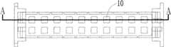
图3是图2的A-A线方向截面图;Fig. 3 is a sectional view along the line A-A of Fig. 2;
图4是本发明LED光源实施例中LED芯片的截面示意图;4 is a schematic cross-sectional view of an LED chip in an embodiment of the LED light source of the present invention;
图5是本发明LED光源实施例中LED芯片及荧光晶片固定结构的立体分解图;Fig. 5 is a three-dimensional exploded view of the fixing structure of the LED chip and the fluorescent chip in the embodiment of the LED light source of the present invention;
图6是本发明LED光源的实施例三的侧面示意图;Fig. 6 is a schematic side view of Embodiment 3 of the LED light source of the present invention;
图7是本发明LED光源的实施例四的侧面示意图;Fig. 7 is a schematic side view of Embodiment 4 of the LED light source of the present invention;
图8是本发明LED光源的实施例五的侧面示意图;Fig. 8 is a schematic side view of Embodiment 5 of the LED light source of the present invention;
图9是本发明LED光源的实施例六的侧面示意图;Fig. 9 is a schematic side view of Embodiment 6 of the LED light source of the present invention;
图10是本发明LED光源实施例七的侧面示意图;Fig. 10 is a schematic side view of Embodiment 7 of the LED light source of the present invention;
图11是本发明LED光源实施例八的侧面示意图;Fig. 11 is a schematic side view of the eighth embodiment of the LED light source of the present invention;
图12是本发明LED光源实施例九的平面示意图;Fig. 12 is a schematic plan view of Embodiment 9 of the LED light source of the present invention;
图13是本发明LED光源实施例十的平面示意图;13 is a schematic plan view of
图14是本发明LED光源实施例十一的侧面示意图;Fig. 14 is a schematic side view of the eleventh embodiment of the LED light source of the present invention;
图15是图14的平面示意图;Figure 15 is a schematic plan view of Figure 14;
图16是本发明LED光源实施例十二的侧面示意图;Fig. 16 is a schematic side view of Embodiment 12 of the LED light source of the present invention;
图17是本发明LED光源实施例十三的侧面示意图;Fig. 17 is a schematic side view of
图18是本发明LED光源实施例十四的侧面示意图;Fig. 18 is a schematic side view of
图19是本发明LED光源实施例十五的侧面示意图;Fig. 19 is a schematic side view of
图20是本发明LED光源实施例十六的侧面示意图。Fig. 20 is a schematic side view of Embodiment 16 of the LED light source of the present invention.
具体实施方式Detailed ways
为详细说明本发明的技术内容、构造特征、所实现目的及效果,以下结合实施方式并配合附图详予说明。In order to describe the technical content, structural features, achieved goals and effects of the present invention in detail, the following will be described in detail in conjunction with the embodiments and accompanying drawings.
参阅图1,本发明LED光源实施例一包括:Referring to Figure 1, Embodiment 1 of the LED light source of the present invention includes:
LED芯片10,包括相背的第一发光面11和第二发光面12;The
对应所述第一发光面11设置的第一荧光体20;a
对应所述第二发光面12设置的第二荧光体30。The
本发明在LED芯片10发光两面都设置荧光体,两面都可以发光,发光效率至少提高30%以上;同时,由于LED芯片10不采用散热基座固定的方式,LED芯片10这一面可以通过对流、辐射方式散热,散热设计变得非常简单,散热效果也得到保证。In the present invention, phosphors are arranged on both sides of the
在一实施例中,所述第一荧光体20是荧光胶体,第二荧光体30是荧光胶体;或In one embodiment, the
所述第一荧光体20是荧光晶片,第二荧光体30是荧光胶体;或The
所述第二荧光体30是荧光晶片,第一荧光体20是荧光胶体;或The
所述第一荧光体20是荧光晶片,第二荧光体30是荧光晶片。The
所述荧光晶片可以作为LED芯片10的固定基座,并且可以散热,由于较薄,散热性能可以得以保证。The phosphor wafer can be used as a fixed base for the
所述荧光晶片可以是通过量子分割的含有多种稀土元素的钇铝石榴石YAG晶体等。The fluorescent wafer can be yttrium aluminum garnet YAG crystal containing various rare earth elements through quantum division.
参阅图2和图3,在另一实施例中,所述第一荧光体20和第二荧光体30都是荧光晶片,所述LED芯片10数量为单个或多个,其中,多个所述LED芯片10通过串联或并联连接,水平排列一同位于所述两荧光晶片之间,并且每个LED芯片10之间留有空隙40。Referring to Fig. 2 and Fig. 3, in another embodiment, the
在上述实施例中,将刚性的荧光晶片作为多个LED芯片10固定的基座,免去散热基座结构,体积、发光效率都得到改善;同时,在每个LED芯片10之间留有空隙40,LED芯片10外无树脂等物质包裹,利于将每个LED芯片10的散发的热量直接通过这些空隙40的气体散发出去,进一步保证热量能够迅速散开,也保证LED芯片10在较低温度下正常工作,提高寿命。In the above-mentioned embodiment, the rigid fluorescent wafer is used as a fixed base for a plurality of
在另一实施例中,所述第一荧光体20和第二荧光体30都是荧光晶片,并且平行设置,所述LED芯片10为无反光层的双面出光的正装芯片或倒装芯片。In another embodiment, both the
一起参阅图2、图3和图4,对于倒装芯片,即P极和N极都位于芯片同一面结构,所述倒装芯片无电极一面通过分子键合固定于一所述荧光晶片,或者通过高透光高导热固晶胶固定于一所述荧光晶片表面后进行串并联。对于正装芯片,即P极和N极分别位于LED芯片10相背两面结构,所述正装芯片采用架空支架架空在所述两块荧光晶片之间(参阅图16或图17),其中所述架空支架位于两块荧光晶片之间,LED芯片10的两侧边分别接所述架空支架,使得LED芯片10悬于所述两块荧光晶片之间。Referring to Fig. 2, Fig. 3 and Fig. 4 together, for the flip chip, that is, the P pole and the N pole are all located on the same surface of the chip, and the electrodeless side of the flip chip is fixed to a fluorescent wafer by molecular bonding, or After being fixed on the surface of a fluorescent chip by a high-transmittance and high-thermal-conductivity crystal-bonding adhesive, the series-parallel connection is performed. For the front-mounted chip, that is, the P pole and the N pole are respectively located on the opposite sides of the
对于倒装芯片的结构,可以是倒装结构的六面发光体,包括依次层叠的透明刚性基底13、发光层14以及电流扩散层15,所述透明刚性基底13固定于一所述荧光晶片表面,另一所述荧光晶片对应所述电流扩散层15一侧设置。For the flip-chip structure, it can be a hexahedral illuminant with a flip-chip structure, including a transparent
本实施例利用倒装结构的LED来实现双面发光,易于实现。In this embodiment, LEDs with a flip-chip structure are used to realize double-sided light emission, which is easy to implement.
在另一实施例中,所述透明刚性基底13是蓝宝石,所述蓝宝石通过键合方式与所述荧光晶片固定。In another embodiment, the transparent
由于通过键合方式固定,省略了导热硅胶等导热介质,避免导热介质导热性能低而形成的导热瓶颈,使散热性能进一步提高。当然,所述透明刚性衬底13也可以是其他透明的刚性物体,包括能够以键合方式与所述荧光晶片固定的物体。Since it is fixed by bonding, heat conduction medium such as heat conduction silica gel is omitted, and the heat conduction bottleneck formed by the low heat conduction performance of heat conduction medium is avoided, so that the heat dissipation performance is further improved. Certainly, the transparent
所述LED芯片10也可以是两面出光的发光体,没有蓝宝石作为衬底。其中,至少所述第二荧光体30和所述LED芯片10通过键合方式相互固定。比如,材质为荧光晶片的第二荧光体30与所述LED芯片10无电极的一面进行键合。因为LED芯片10是半导体裸片,与第二荧光体30直接键合,大大减少厚度并且节省成本。The
一起参阅图3和图5,在另一实施例中,两所述荧光晶片之间设置有多个互相隔开的所述LED芯片10,两所述荧光晶片之间通过位于荧光晶片周围的粘结剂50粘结,并通过分布于两荧光晶片相对表面设置的多个支撑柱60间隔固定,两所述荧光晶片之间充有惰性气体(图未示),如高导热性能的惰性气体,可以是氦气或氢气的等,两所述荧光晶片之间的所述粘结剂50设有多个透气孔70。Referring to Fig. 3 and Fig. 5 together, in another embodiment, a plurality of said
本实施例将两荧光晶片之间的空间作为LED芯片10的容置空间,同时留有此容置空间与外界互通的透气孔70,形成散热通道,利于散热。In this embodiment, the space between the two fluorescent chips is used as the accommodating space for the
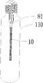
所述粘结剂50是光反射粘结硅胶,所述光反射粘结硅胶上设有电极81,所述电流扩散层15上设置有P型结,所述发光层14邻近电流扩散层15的一侧设有N型结,所述多个LED芯片10之间通过串联或并联的方式采用金线80连接各LED芯片10的P型结和N型结,所述金线80连接至所述电极81。当然,也可以采用铜线等导线。The adhesive 50 is a light-reflective bonding silica gel, an
参阅图3,其中,还包括夹固所述两荧光晶片边侧的夹持机构90。Referring to FIG. 3 , it also includes a
本实施例利用夹持机构90夹持两荧光晶片,使得LED芯片10与荧光晶片之间直接接触,相比于采用粘结剂50连接方式更进一步提高散热效率,并且结构简单实用。In this embodiment, the
本发明可以应用于各种光源,比如灯泡,比如应急灯、PAR灯、车灯、路灯、隧道灯、室内照明灯等。The present invention can be applied to various light sources, such as light bulbs, such as emergency lights, PAR lights, car lights, street lights, tunnel lights, indoor lighting and the like.
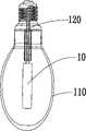
参阅图6,在一个实施例中,所述LED光源是泡灯,包括灯泡110和填充灯泡110的惰性气体(图未示),所述荧光晶片和LED芯片10位于灯泡110内,所述两荧光晶片之间的空间通过所述透气孔70(图5)连通两荧光晶片之外的所述灯泡110空间。6, in one embodiment, the LED light source is a bulb lamp, including a
利用灯泡110内的惰性气体作为灯泡110外空间与LED芯片10之间的散热媒介,把整个灯泡110外表面作为散热表面,大幅提高散热表面,提高散热性能;同时惰性气体能保证LED芯片10不会被氧化,保证长期使用性能。The inert gas in the
参阅图7和图8,在一个实施例中,所述泡灯可以包括连通所述荧光晶片内空间的气道120。Referring to FIG. 7 and FIG. 8 , in one embodiment, the bulb lamp may include an
参阅图9,所述泡灯是PAR灯,包括外壳130和内壳140,所述外壳130具有连通外壳130与内壳140之间空间和外界的通孔150。Referring to FIG. 9 , the bulb lamp is a PAR lamp, which includes an
参阅图10,在一个实施例中,包括设置于所述两荧光晶片一边侧的反光杯160,使LED芯片10所有表面的发出的光线都被反光杯160朝一个方向反射,适合于限定范围发光的场景。Referring to Fig. 10, in one embodiment, it includes a
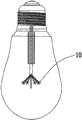
参阅图11,在一个实施例中,一个泡灯里面设有多个扩散状连接端的支架(未标示),每个所述连接端连接一个LED芯片10。Referring to FIG. 11 , in one embodiment, a bulb is provided with a plurality of brackets (not shown) with diffused connection ends, each of which is connected to an
参阅图12和图13,所述荧光晶片可以是矩形结构,也可以是圆形等结构。Referring to FIG. 12 and FIG. 13 , the phosphor wafer can be in a rectangular structure, or in a circular structure.
参阅图14和图15,两片荧光晶片之间可以仅设置一颗LED芯片10,两片荧光晶片的两端采用夹持机构90夹持固定。在仅设置一颗LED芯片10的情况下,也可以不采用LED倒装结构。Referring to FIG. 14 and FIG. 15 , only one
参阅图18、19、20,所述泡灯的形状还可以是多节型、尖形或烧杯型等。Referring to Figures 18, 19, and 20, the shape of the bulb can also be multi-section, pointed, or beaker.
与传统光源一样,半导体LED在工作期间也会产生热量,其多少取决于整体的发光效率。现有技术中,在外加电能量作用下,电子和空穴的辐射复合电致发光,在PN结附近辐射出来的光还需经过芯片本身的半导体介质和封装介质才能抵达外界。其综合电流注入效率、辐射发光量子效率、芯片外部光取出效率等,最终大概只有30%~40%的输入电能转化为光能,其余70%的能量转化为热能。需要说明的是热量管理是在LED产品的发光效率不高的现阶段的关键问题,从根本上提高发光效率以减少热能的产生才是釜底抽薪之举。Like traditional light sources, semiconductor LEDs also generate heat during operation, the amount of which depends on the overall luminous efficiency. In the prior art, under the action of external electric energy, electrons and holes radiate and recombine to electroluminescence, and the light radiated near the PN junction needs to pass through the semiconductor medium and packaging medium of the chip itself to reach the outside world. Its comprehensive current injection efficiency, radiation luminescence quantum efficiency, chip external light extraction efficiency, etc., in the end, only about 30% to 40% of the input electric energy is converted into light energy, and the remaining 70% of the energy is converted into heat energy. What needs to be explained is that heat management is the key issue at the current stage when the luminous efficiency of LED products is not high. Fundamentally improving the luminous efficiency to reduce the generation of heat energy is a drastic move.
本发明克服长期以来需要专门的LED散热基座作为承载体的技术偏见,不采用专门的散热基座,利用LED芯片10双面发光的特点,无角度限制地利用了所有方向的光能,可以提升30%以上的光能利用率;同时,彻底解决了散热基座形成的散热瓶颈,全角度发光的同时实现全角度的散热,大幅提高发光效率的同时大幅提高散热性能。在散热性能得以提升的情况下,LED芯片10始终在低温下高效工作,电子和空穴辐射复合电致发光的效率大幅提升,形成提高散热性能-提高发光效率-提高散热性能的良性工作循环。经测试,电能转化为可利用光能的效率可以达到85%以上;The present invention overcomes the long-standing technical prejudice that requires a special LED heat dissipation base as a carrier, does not use a special heat dissipation base, utilizes the double-sided light emitting characteristics of the
此外,裸露的LED芯片与惰性气体直接接触进行热交换的设计,能进一步降低LED芯片工作温度,在上述85%光能可利用率的基础上进一步提升至90%以上,效果极为明显。In addition, the design of direct contact between the exposed LED chip and the inert gas for heat exchange can further reduce the operating temperature of the LED chip, and further increase the utilization rate of light energy to more than 90% on the basis of the above-mentioned 85% light energy utilization rate, and the effect is extremely obvious.
以上所述仅为本发明的实施例,并非因此限制本发明的专利范围,凡是利用本发明说明书及附图内容所作的等效结构或等效流程变换,或直接或间接运用在其他相关的技术领域,均同理包括在本发明的专利保护范围内。The above is only an embodiment of the present invention, and does not limit the patent scope of the present invention. Any equivalent structure or equivalent process transformation made by using the description of the present invention and the contents of the accompanying drawings, or directly or indirectly used in other related technologies fields, all of which are equally included in the scope of patent protection of the present invention.
Claims (10)
Priority Applications (9)
| Application Number | Priority Date | Filing Date | Title |
|---|---|---|---|
| CN201010172360ACN101846256A (en) | 2010-05-04 | 2010-05-04 | LED light source |
| AU2011250561AAU2011250561B2 (en) | 2010-05-04 | 2011-04-29 | LED light source and manufacturing method thereof |
| SG2012080974ASG185402A1 (en) | 2010-05-04 | 2011-04-29 | Led light source and manufacturing method thereof |
| RU2012153464/07ARU2587999C2 (en) | 2010-05-04 | 2011-04-29 | Led light source and method of making same |
| EP11777083.4AEP2567145B1 (en) | 2010-05-04 | 2011-04-29 | Led light source and manufacturing method thereof |
| KR1020127031810AKR101621811B1 (en) | 2010-05-04 | 2011-04-29 | LED light source and Manufacturing Method Thereof |
| PCT/CN2011/000756WO2011137662A1 (en) | 2010-05-04 | 2011-04-29 | Led light source and manufacturing method thereof |
| JP2013508356AJP2013531367A (en) | 2010-05-04 | 2011-04-29 | LED light source and manufacturing method thereof |
| US13/068,162US8534866B2 (en) | 2010-05-04 | 2011-05-03 | LED light source |
Applications Claiming Priority (1)
| Application Number | Priority Date | Filing Date | Title |
|---|---|---|---|
| CN201010172360ACN101846256A (en) | 2010-05-04 | 2010-05-04 | LED light source |
Publications (1)
| Publication Number | Publication Date |
|---|---|
| CN101846256Atrue CN101846256A (en) | 2010-09-29 |
Family
ID=42770977
Family Applications (1)
| Application Number | Title | Priority Date | Filing Date |
|---|---|---|---|
| CN201010172360APendingCN101846256A (en) | 2010-05-04 | 2010-05-04 | LED light source |
Country Status (8)
| Country | Link |
|---|---|
| US (1) | US8534866B2 (en) |
| EP (1) | EP2567145B1 (en) |
| JP (1) | JP2013531367A (en) |
| KR (1) | KR101621811B1 (en) |
| CN (1) | CN101846256A (en) |
| AU (1) | AU2011250561B2 (en) |
| SG (1) | SG185402A1 (en) |
| WO (1) | WO2011137662A1 (en) |
Cited By (16)
| Publication number | Priority date | Publication date | Assignee | Title |
|---|---|---|---|---|
| CN102720987A (en)* | 2012-05-25 | 2012-10-10 | 苏州晶品光电科技有限公司 | Light emitting diode (LED) area source employing side light emitting bar |
| CN102759024A (en)* | 2011-04-26 | 2012-10-31 | 蔡州 | LED (Light Emitting Diode) light source and manufacturing method thereof |
| CN102800800A (en)* | 2012-08-28 | 2012-11-28 | 安徽三安光电有限公司 | Light-emitting diode device and production method thereof |
| CN102903827A (en)* | 2012-09-21 | 2013-01-30 | 威力盟电子(苏州)有限公司 | Packaging structure and packaging method of light emitting diode |
| CN102903831A (en)* | 2012-05-15 | 2013-01-30 | 北京工业大学 | Structure and preparation process of a white light LED |
| CN103456870A (en)* | 2013-09-11 | 2013-12-18 | 厦门华联电子有限公司 | COB light source coated by fluorescent powder glue and manufacturing method thereof |
| CN103456869A (en)* | 2012-05-29 | 2013-12-18 | 璨圆光电股份有限公司 | Light-emitting device, light-emitting diode chip for forming multi-directional light emission and sapphire substrate thereof |
| WO2015062293A1 (en)* | 2013-10-29 | 2015-05-07 | 蔡鸿 | Led light source heat dissipation structure and heat dissipation method thereof |
| WO2015074551A1 (en)* | 2013-11-21 | 2015-05-28 | 何文铭 | Led module structure, and manufacturing process for led module |
| WO2016029809A1 (en)* | 2014-08-26 | 2016-03-03 | 蔡鸿 | Led direct-lit backlight source and light emission method therefor |
| CN106340510A (en)* | 2015-07-03 | 2017-01-18 | 华润矽威科技(上海)有限公司 | Light-emitting assembly and light-electricity integrated lighting device |
| CN109737359A (en)* | 2019-03-15 | 2019-05-10 | 华域视觉科技(上海)有限公司 | Luminous body and its manufacturing method, surface emitting light source, vehicle lamp, automobile |
| CN110350064A (en)* | 2013-07-01 | 2019-10-18 | 晶元光电股份有限公司 | Light-emitting diode component and production method |
| CN111129956A (en)* | 2019-12-07 | 2020-05-08 | 武汉高跃科技有限责任公司 | Multi-chip pulse tail laser assembly |
| EP2535640B2 (en)† | 2010-09-08 | 2020-09-23 | Zhejiang Ledison Optoelectronics Co., Ltd. | Led lamp bulb and led lighting bar capable of emitting light over 4 pi |
| US12259096B2 (en) | 2011-02-22 | 2025-03-25 | Quarkstar Llc | Solid state lamp using light emitting strips |
Families Citing this family (45)
| Publication number | Priority date | Publication date | Assignee | Title |
|---|---|---|---|---|
| US10655792B2 (en) | 2014-09-28 | 2020-05-19 | Zhejiang Super Lighting Electric Appliance Co., Ltd. | LED bulb lamp |
| US9995474B2 (en) | 2015-06-10 | 2018-06-12 | Jiaxing Super Lighting Electric Appliance Co., Ltd. | LED filament, LED filament assembly and LED bulb |
| US10544905B2 (en) | 2014-09-28 | 2020-01-28 | Zhejiang Super Lighting Electric Appliance Co., Ltd. | LED bulb lamp |
| US10473271B2 (en) | 2015-08-17 | 2019-11-12 | Zhejiang Super Lighting Electric Appliance Co., Ltd. | LED filament module and LED light bulb |
| US10240724B2 (en) | 2015-08-17 | 2019-03-26 | Zhejiang Super Lighting Electric Appliance Co., Ltd. | LED filament |
| US10677396B2 (en) | 2006-07-22 | 2020-06-09 | Jiaxing Super Lighting Electric Appliance Co., Ltd | LED light bulb with symmetrical filament |
| US10487987B2 (en) | 2015-08-17 | 2019-11-26 | Zhejiang Super Lighting Electric Appliance Co., Ltd. | LED filament |
| CN103762211A (en)* | 2011-12-31 | 2014-04-30 | 苏州晶品光电科技有限公司 | Flexible circuit substrate double-sided light-emitting LED array light source |
| CN102709452A (en)* | 2012-05-21 | 2012-10-03 | 苏州晶品光电科技有限公司 | Fluorescent transparent ceramic LED (light-emitting diode) sealing structure and sealing method thereof |
| US20140085873A1 (en)* | 2012-09-21 | 2014-03-27 | Nolan Willis | Style Tyle |
| CN103236485B (en)* | 2013-04-16 | 2016-01-13 | 哈尔滨鎏霞光电技术有限公司 | A kind of method making luminous element on sapphire transparent heat-conducting plate |
| CN103325921B (en)* | 2013-06-04 | 2016-04-20 | 苏州晶品新材料股份有限公司 | High heat conduction fluorescence insulation LED package structure |
| TWI626395B (en) | 2013-06-11 | 2018-06-11 | 晶元光電股份有限公司 | Illuminating device |
| JP2015171040A (en)* | 2014-03-07 | 2015-09-28 | 株式会社ダイトク | Dead angle reduction method for led street light having built-in crime prevention camera |
| CN103956421A (en)* | 2014-04-22 | 2014-07-30 | 中国科学院上海光学精密机械研究所 | LED lamp based on transparent fluorescent ceramics |
| TWM496848U (en)* | 2014-07-30 | 2015-03-01 | Yu-Yu Gao | Fluorescent composite resin substrate white light emitting diode |
| US11085591B2 (en) | 2014-09-28 | 2021-08-10 | Zhejiang Super Lighting Electric Appliance Co., Ltd | LED light bulb with curved filament |
| US11997768B2 (en) | 2014-09-28 | 2024-05-28 | Zhejiang Super Lighting Electric Appliance Co., Ltd | LED filament and LED light bulb |
| US11028970B2 (en) | 2014-09-28 | 2021-06-08 | Zhejiang Super Lighting Electric Appliance Co., Ltd | LED filament light bulb having organosilicon-modified polyimide resin composition filament base layer |
| US11259372B2 (en) | 2015-06-10 | 2022-02-22 | Zhejiang Super Lighting Electric Appliance Co., Ltd | High-efficiency LED light bulb with LED filament therein |
| US10845008B2 (en) | 2014-09-28 | 2020-11-24 | Zhejiang Super Lighting Electric Appliance Co., Ltd. | LED filament and LED light bulb |
| US12007077B2 (en) | 2014-09-28 | 2024-06-11 | Zhejiang Super Lighting Electric Appliance Co., Ltd. | LED filament and LED light bulb |
| US10976009B2 (en) | 2014-09-28 | 2021-04-13 | Zhejiang Super Lighting Electric Appliance Co., Ltd | LED filament light bulb |
| US10784428B2 (en) | 2014-09-28 | 2020-09-22 | Zhejiang Super Lighting Electric Appliance Co., Ltd. | LED filament and LED light bulb |
| US11015764B2 (en) | 2014-09-28 | 2021-05-25 | Zhejiang Super Lighting Electric Appliance Co., Ltd | LED light bulb with flexible LED filament having perpendicular connecting wires |
| US11543083B2 (en) | 2014-09-28 | 2023-01-03 | Zhejiang Super Lighting Electric Appliance Co., Ltd | LED filament and LED light bulb |
| US11686436B2 (en) | 2014-09-28 | 2023-06-27 | Zhejiang Super Lighting Electric Appliance Co., Ltd | LED filament and light bulb using LED filament |
| US12313227B2 (en) | 2014-09-28 | 2025-05-27 | Zhejiang Super Lighting Electric Appliance Co., Ltd. | LED filament and LED light bulb |
| US11421827B2 (en) | 2015-06-19 | 2022-08-23 | Zhejiang Super Lighting Electric Appliance Co., Ltd | LED filament and LED light bulb |
| US11525547B2 (en) | 2014-09-28 | 2022-12-13 | Zhejiang Super Lighting Electric Appliance Co., Ltd | LED light bulb with curved filament |
| US11073248B2 (en) | 2014-09-28 | 2021-07-27 | Zhejiang Super Lighting Electric Appliance Co., Ltd. | LED bulb lamp |
| US10982816B2 (en) | 2014-09-28 | 2021-04-20 | Zhejiang Super Lighting Electric Appliance Co., Ltd | LED light bulb having uniform light emmision |
| TWI570352B (en)* | 2014-11-28 | 2017-02-11 | 宏齊科技股份有限公司 | Light-emitting diode device and light-emitting device using same |
| FR3034838B1 (en)* | 2015-04-08 | 2017-03-31 | Led-Ner | LED FILAMENT LIGHTING DEVICE |
| KR101776917B1 (en) | 2015-05-14 | 2017-09-08 | 이민우 | Composite light-emitting element of the sandwich-type fine pattern |
| GB2543139B (en)* | 2015-08-17 | 2018-05-23 | Jiaxing Super Lighting Electric Appliance Co Ltd | LED light bulb and LED filament thereof |
| US11168844B2 (en) | 2015-08-17 | 2021-11-09 | Zhejiang Super Lighting Electric Appliance Co., Ltd | LED light bulb having filament with segmented light conversion layer |
| US10359152B2 (en) | 2015-08-17 | 2019-07-23 | Zhejiang Super Lighting Electric Appliance Co, Ltd | LED filament and LED light bulb |
| CN107492545A (en)* | 2016-06-09 | 2017-12-19 | 王定锋 | The LED circuit board encapsulation module and preparation method of three-dimensional multifaceted light-emitting |
| CN106653979A (en)* | 2016-12-27 | 2017-05-10 | 左洪波 | Fabrication method of high-efficiency Q-LED package structure |
| TWI638116B (en)* | 2017-09-01 | 2018-10-11 | 液光固態照明股份有限公司 | Led light bulb and manufacturing method thereof |
| WO2019129034A1 (en) | 2017-12-26 | 2019-07-04 | 嘉兴山蒲照明电器有限公司 | Light-emitting diode filament and light-emitting diode bulb |
| US10790419B2 (en) | 2017-12-26 | 2020-09-29 | Jiaxing Super Lighting Electric Appliance Co., Ltd | LED filament and LED light bulb |
| US10982048B2 (en) | 2018-04-17 | 2021-04-20 | Jiaxing Super Lighting Electric Appliance Co., Ltd | Organosilicon-modified polyimide resin composition and use thereof |
| JP7472558B2 (en) | 2020-03-12 | 2024-04-23 | セイコーエプソン株式会社 | Wavelength conversion element, light source device, projector, and method for manufacturing wavelength conversion element |
Citations (3)
| Publication number | Priority date | Publication date | Assignee | Title |
|---|---|---|---|---|
| CN1617361A (en)* | 2003-11-10 | 2005-05-18 | 光宝科技股份有限公司 | white light emitting device |
| CN101312185A (en)* | 2007-03-23 | 2008-11-26 | 夏普株式会社 | Light emitting device and method for manufacturing the same |
| CN101501871A (en)* | 2006-01-31 | 2009-08-05 | 京瓷株式会社 | Light emitting apparatus and light emitting module |
Family Cites Families (21)
| Publication number | Priority date | Publication date | Assignee | Title |
|---|---|---|---|---|
| JP3300778B2 (en)* | 1999-10-05 | 2002-07-08 | ラボ・スフィア株式会社 | Luminous body |
| EP1264353A2 (en)* | 2000-03-06 | 2002-12-11 | Teledyne Lighting and Display Products, Inc. | Lighting apparatus having quantum dot layer |
| EP1467414A4 (en)* | 2001-12-29 | 2007-07-11 | Hangzhou Fuyang Xinying Dianzi | A led and led lamp |
| JP4072632B2 (en)* | 2002-11-29 | 2008-04-09 | 豊田合成株式会社 | Light emitting device and light emitting method |
| JP2004193393A (en)* | 2002-12-12 | 2004-07-08 | Matsushita Electric Ind Co Ltd | Composite light emitting device |
| CN100590898C (en)* | 2004-07-29 | 2010-02-17 | 昭和电工株式会社 | Positive electrode for semiconductor light emitting devices |
| JP2006202612A (en)* | 2005-01-20 | 2006-08-03 | Momo Alliance Co Ltd | Light emission device and lighting system |
| JP4756682B2 (en)* | 2005-05-16 | 2011-08-24 | シチズン電子株式会社 | Light emitting diode light source unit and bulb type light emitting diode light source |
| JP2007042985A (en)* | 2005-08-05 | 2007-02-15 | Showa Denko Kk | Gallium-nitride-based compound semiconductor light-emitting device and packaging body thereof |
| CA2624507C (en)* | 2005-10-07 | 2014-04-29 | Osram Sylvania Inc. | Led with light transmissive heat sink |
| TWI296895B (en)* | 2005-12-02 | 2008-05-11 | Au Optronics Corp | Encapsulation structure of dual emission organic electroluminescence device and method of fabricating the same |
| JP2007165811A (en)* | 2005-12-16 | 2007-06-28 | Nichia Chem Ind Ltd | Light emitting device |
| WO2007130358A2 (en)* | 2006-05-02 | 2007-11-15 | Superbulbs, Inc. | Plastic led bulb |
| JP2008034473A (en)* | 2006-07-26 | 2008-02-14 | Toyoda Gosei Co Ltd | Surface light source |
| US8148746B2 (en)* | 2006-09-29 | 2012-04-03 | Rohm Co., Ltd. | Semiconductor light emitting device |
| CN101210664A (en)* | 2006-12-29 | 2008-07-02 | 富准精密工业(深圳)有限公司 | Light-emitting diode lamps and lanterns |
| CN100573964C (en)* | 2006-12-30 | 2009-12-23 | 财团法人工业技术研究院 | organic light emitting diode |
| DE102007017113A1 (en)* | 2007-01-31 | 2008-08-07 | Osram Opto Semiconductors Gmbh | Semiconductor device with an optically active layer, arrangement with a plurality of optically active layers and method for producing a semiconductor device |
| JP2009071090A (en)* | 2007-09-14 | 2009-04-02 | Toshiba Lighting & Technology Corp | Light emitting device |
| US20090140279A1 (en)* | 2007-12-03 | 2009-06-04 | Goldeneye, Inc. | Substrate-free light emitting diode chip |
| DE102008008599A1 (en)* | 2007-12-20 | 2009-06-25 | Osram Opto Semiconductors Gmbh | Light-emitting semiconductor component has epitaxially grown semiconductor layer sequence with sublayer suitable for light generation and electrical contacts, which are contacting semiconductor layer sequence |
- 2010
- 2010-05-04CNCN201010172360Apatent/CN101846256A/enactivePending
- 2011
- 2011-04-29JPJP2013508356Apatent/JP2013531367A/enactivePending
- 2011-04-29AUAU2011250561Apatent/AU2011250561B2/ennot_activeCeased
- 2011-04-29WOPCT/CN2011/000756patent/WO2011137662A1/enactiveApplication Filing
- 2011-04-29EPEP11777083.4Apatent/EP2567145B1/ennot_activeNot-in-force
- 2011-04-29KRKR1020127031810Apatent/KR101621811B1/ennot_activeExpired - Fee Related
- 2011-04-29SGSG2012080974Apatent/SG185402A1/enunknown
- 2011-05-03USUS13/068,162patent/US8534866B2/enactiveActive
Patent Citations (3)
| Publication number | Priority date | Publication date | Assignee | Title |
|---|---|---|---|---|
| CN1617361A (en)* | 2003-11-10 | 2005-05-18 | 光宝科技股份有限公司 | white light emitting device |
| CN101501871A (en)* | 2006-01-31 | 2009-08-05 | 京瓷株式会社 | Light emitting apparatus and light emitting module |
| CN101312185A (en)* | 2007-03-23 | 2008-11-26 | 夏普株式会社 | Light emitting device and method for manufacturing the same |
Cited By (22)
| Publication number | Priority date | Publication date | Assignee | Title |
|---|---|---|---|---|
| EP2535640B2 (en)† | 2010-09-08 | 2020-09-23 | Zhejiang Ledison Optoelectronics Co., Ltd. | Led lamp bulb and led lighting bar capable of emitting light over 4 pi |
| US12259096B2 (en) | 2011-02-22 | 2025-03-25 | Quarkstar Llc | Solid state lamp using light emitting strips |
| CN102759024B (en)* | 2011-04-26 | 2015-03-04 | 蔡州 | LED (Light Emitting Diode) light source and manufacturing method thereof |
| CN102759024A (en)* | 2011-04-26 | 2012-10-31 | 蔡州 | LED (Light Emitting Diode) light source and manufacturing method thereof |
| CN102903831A (en)* | 2012-05-15 | 2013-01-30 | 北京工业大学 | Structure and preparation process of a white light LED |
| CN102720987A (en)* | 2012-05-25 | 2012-10-10 | 苏州晶品光电科技有限公司 | Light emitting diode (LED) area source employing side light emitting bar |
| CN103456869A (en)* | 2012-05-29 | 2013-12-18 | 璨圆光电股份有限公司 | Light-emitting device, light-emitting diode chip for forming multi-directional light emission and sapphire substrate thereof |
| CN103456869B (en)* | 2012-05-29 | 2016-12-28 | 晶元光电股份有限公司 | Light-emitting device, light-emitting diode chip for forming multi-directional light emission and sapphire substrate thereof |
| CN102800800A (en)* | 2012-08-28 | 2012-11-28 | 安徽三安光电有限公司 | Light-emitting diode device and production method thereof |
| CN102903827A (en)* | 2012-09-21 | 2013-01-30 | 威力盟电子(苏州)有限公司 | Packaging structure and packaging method of light emitting diode |
| CN110350064A (en)* | 2013-07-01 | 2019-10-18 | 晶元光电股份有限公司 | Light-emitting diode component and production method |
| CN103456870A (en)* | 2013-09-11 | 2013-12-18 | 厦门华联电子有限公司 | COB light source coated by fluorescent powder glue and manufacturing method thereof |
| CN103456870B (en)* | 2013-09-11 | 2016-06-01 | 厦门华联电子有限公司 | The COB light source of phosphor gel coating and manufacture method thereof |
| CN106030207B (en)* | 2013-10-29 | 2019-04-05 | 蔡鸿 | A heat dissipation structure of an LED light source and a heat dissipation method thereof |
| CN106030207A (en)* | 2013-10-29 | 2016-10-12 | 蔡鸿 | LED light source heat dissipation structure and heat dissipation method thereof |
| WO2015062293A1 (en)* | 2013-10-29 | 2015-05-07 | 蔡鸿 | Led light source heat dissipation structure and heat dissipation method thereof |
| WO2015074551A1 (en)* | 2013-11-21 | 2015-05-28 | 何文铭 | Led module structure, and manufacturing process for led module |
| WO2016029809A1 (en)* | 2014-08-26 | 2016-03-03 | 蔡鸿 | Led direct-lit backlight source and light emission method therefor |
| CN106340510A (en)* | 2015-07-03 | 2017-01-18 | 华润矽威科技(上海)有限公司 | Light-emitting assembly and light-electricity integrated lighting device |
| CN106340510B (en)* | 2015-07-03 | 2019-08-23 | 华润矽威科技(上海)有限公司 | Luminescence component and optoelectronic integration lighting device |
| CN109737359A (en)* | 2019-03-15 | 2019-05-10 | 华域视觉科技(上海)有限公司 | Luminous body and its manufacturing method, surface emitting light source, vehicle lamp, automobile |
| CN111129956A (en)* | 2019-12-07 | 2020-05-08 | 武汉高跃科技有限责任公司 | Multi-chip pulse tail laser assembly |
Also Published As
| Publication number | Publication date |
|---|---|
| RU2012153464A (en) | 2014-06-10 |
| KR101621811B1 (en) | 2016-05-17 |
| AU2011250561A1 (en) | 2013-01-10 |
| EP2567145A1 (en) | 2013-03-13 |
| EP2567145B1 (en) | 2016-04-20 |
| JP2013531367A (en) | 2013-08-01 |
| SG185402A1 (en) | 2012-12-28 |
| US20110273863A1 (en) | 2011-11-10 |
| US8534866B2 (en) | 2013-09-17 |
| EP2567145A4 (en) | 2014-03-19 |
| AU2011250561B2 (en) | 2015-01-22 |
| WO2011137662A1 (en) | 2011-11-10 |
| KR20130114578A (en) | 2013-10-17 |
Similar Documents
| Publication | Publication Date | Title |
|---|---|---|
| CN101846256A (en) | LED light source | |
| KR20150013449A (en) | Led lighting column and led lamp using same | |
| CN102694102B (en) | Light emitting diode packaging structure, manufacturing method thereof, and light source apparatus | |
| CN103633227B (en) | Method and apparatus for manufacturing phosphor coated L ED die | |
| CN103775858B (en) | 4 pi emergent light LED (Light Emitting Diode) light emitting pipe with chip flipped in transparent ceramic tube and illuminating lamp | |
| CN104078548A (en) | Full-angle light-emitting LED white light source and manufacturing method thereof | |
| CN101984510A (en) | Flexibly connected light-emitting diode (LED) device based on liquid metal base | |
| CN103151445B (en) | Low thermal resistance LED (Light Emitting Diode) packaging structure and packaging method | |
| CN103840064A (en) | Three-dimensional luminous LED device and manufacturing method thereof | |
| CN202013881U (en) | Integrated packaging structure with vertically structured LED chips | |
| CN204592952U (en) | A kind of LED silk lamp with radiating piece LED silk | |
| CN110416384A (en) | A packaging method that can improve the pearlescent effect of LED lamps | |
| CN105609496A (en) | High power density COB (Chip On Board) packaged white LED (Light Emitting Diode) module and packaging method thereof | |
| CN106848032B (en) | A wafer-level packaged LED device structure | |
| CN103996785A (en) | Built-in drive full-angle light-emitting LED light source and packaging process | |
| WO2008055406A1 (en) | A white light led | |
| CN203456457U (en) | SMD LED structure characterized by polycrystalline packaging | |
| CN103715190A (en) | Luminescence device | |
| CN102322584A (en) | Ultrathin LED (light-emitting diode) surface light source based on COB (chip on board) packaging technology | |
| CN201725811U (en) | Led light source | |
| CN103489995A (en) | Flexible LED (light-emitting diode) light source filament | |
| CN204857721U (en) | High -power LED encapsulation paster | |
| CN108321278A (en) | A kind of LED packagings | |
| CN106876567A (en) | Height radiating diode package structure | |
| CN103165792A (en) | Light emitting diode (LED) heat-dissipation packaging structure, LED light and manufacturing method of LED heat-dissipation packaging structure |
Legal Events
| Date | Code | Title | Description |
|---|---|---|---|
| C06 | Publication | ||
| PB01 | Publication | ||
| C10 | Entry into substantive examination | ||
| SE01 | Entry into force of request for substantive examination | ||
| C12 | Rejection of a patent application after its publication | ||
| RJ01 | Rejection of invention patent application after publication | Application publication date:20100929 |