CN101844272A - Method and system for manufacturing self-cleaning surface structure by adopting laser interference photoetching technology - Google Patents
Method and system for manufacturing self-cleaning surface structure by adopting laser interference photoetching technologyDownload PDFInfo
- Publication number
- CN101844272A CN101844272ACN201010101488ACN201010101488ACN101844272ACN 101844272 ACN101844272 ACN 101844272ACN 201010101488 ACN201010101488 ACN 201010101488ACN 201010101488 ACN201010101488 ACN 201010101488ACN 101844272 ACN101844272 ACN 101844272A
- Authority
- CN
- China
- Prior art keywords
- interference
- self
- laser
- cleaning
- material surface
- Prior art date
- Legal status (The legal status is an assumption and is not a legal conclusion. Google has not performed a legal analysis and makes no representation as to the accuracy of the status listed.)
- Pending
Links
Images

Landscapes
- Exposure And Positioning Against Photoresist Photosensitive Materials (AREA)
- Micromachines (AREA)
Abstract
Description
Translated fromChinese技术领域technical field
本发明涉及一种采用激光干涉光刻技术制作材料自清洁表面结构的方法和系统,属于对仿生自清洁表面结构制备技术的改进。The invention relates to a method and system for fabricating self-cleaning surface structures of materials by using laser interference photolithography technology, which belongs to the improvement of the bionic self-cleaning surface structure preparation technology.
技术背景technical background
目前建筑上常被采用的耐沾污方法之一是选用低表面能的材料,涂覆在建筑物表面,污染物就很难稳定附着在漆膜表面。一些自清洁钢化玻璃也采用TiO2复合溶液喷涂法。但是由于这些自清洁膜的材料与基体材料的成分不同,其不同的化学和物理性质将导致其附着力和耐久性受限。并且在钢化玻璃的制造过程中经过不同的温度处理,自清洁膜层的晶型不一样,性能也不同,另外烘干速度大小直接影响晶胞尺寸,从而影响其表面特性。At present, one of the anti-contamination methods commonly used in buildings is to select materials with low surface energy and coat them on the surface of buildings, so that it is difficult for pollutants to adhere stably to the surface of the paint film. Some self-cleaning tempered glass also adopts TiO2 composite solution spraying method. However, since the materials of these self-cleaning films are different from the composition of the base material, their different chemical and physical properties will lead to their limited adhesion and durability. Moreover, in the manufacturing process of tempered glass, after different temperature treatments, the crystal form of the self-cleaning film layer is different, and the performance is also different. In addition, the drying speed directly affects the size of the unit cell, thereby affecting its surface characteristics.
最近研究人员受荷叶自清洁机理的启发,制做保持较长时间的仿生自清洁超疏水表面膜。荷叶表面除了覆盖着一层表面能较低的植物蜡外,蜡质层下的微观结构对其自清洁功能的贡献起着主要作用。这些微结构由众多微米级的乳突所组成,每个微米级的乳突又由许多纳米级的小突起构成,表面的浸润性可从水或油的接触角大小来判断。这种微纳米二级结构,尤其是纳米结构使荷叶表面具有大的水接触角和超疏水性。通常荷叶表面的水接触角为160°,水珠在其上可以自由滚动。荷叶表面的浸润性是由表面蜡质层和其下微结构共同构成,但其微结构对浸润性贡献更大。这给人以启迪,只要构筑合适的仿生微结构,没有低表面能物质也可获得类荷叶的自清洁效应。Recently, inspired by the self-cleaning mechanism of lotus leaves, researchers made a bionic self-cleaning superhydrophobic surface film that can last for a long time. Except that the surface of lotus leaf is covered with a layer of vegetable wax with low surface energy, the microstructure under the waxy layer plays a major role in the contribution of its self-cleaning function. These microstructures are composed of many micron-scale papillae, and each micron-scale papillae is composed of many nanoscale small protrusions. The wettability of the surface can be judged from the contact angle of water or oil. This micro-nano secondary structure, especially the nano-structure, makes the surface of the lotus leaf have a large water contact angle and super-hydrophobicity. Generally, the water contact angle on the surface of the lotus leaf is 160°, and water droplets can roll freely on it. The wettability of the lotus leaf surface is composed of the surface wax layer and the underlying microstructure, but the microstructure contributes more to the wettability. This is inspiring, as long as a suitable biomimetic microstructure is constructed, the self-cleaning effect similar to lotus leaves can be obtained without low surface energy substances.
疏水膜的疏水能力不但受到膜表面形貌的影响,还与这些形貌的微构造的排列及连接方式紧密相关。独立、非连续的柱状排列有利于获得超疏水膜,且其动态前进、后退角差异较小,几乎无粘滞现象,有利于液滴迅速脱离柱头,易于滑落,而这种微结构正是多光束激光干涉图形的显著特点。The hydrophobic ability of the hydrophobic membrane is not only affected by the surface morphology of the membrane, but also closely related to the arrangement and connection mode of the microstructure of these topography. The independent and non-continuous columnar arrangement is conducive to obtaining a superhydrophobic film, and its dynamic advancing and receding angles are small, and there is almost no sticking phenomenon, which is conducive to the rapid detachment of the droplet from the column head and easy sliding. Distinguished features of beam laser interference patterns.
目前在30nm分辨率的范围内,市场上主要有三种直写光刻技术:离子束光刻IBL(ion beamlithography)、电子束光刻EBL(electron beam lithography)和扫描探头光刻SPL(scanningprobe lithography)。SPL可以用功能化的原子力显微镜AFM(atomic force microscope)或扫描隧道显微镜STM(scanning tunnelling microscope)来完成。由于这三种技术均采用耗时的顺序工作方式,其缺点是速度非常慢,不适合批量生产。另一种相关的技术是纳米压印NIL(nano imprint lithography)。NIL提供了一种低成本批量生产纳米表面结构的途径,但其压印的物理特性决定了它的严格使用条件。否则,不完善的表面结构就可随时产生。该技术的缺点是只能使用在清洁的平面,并且它的模板图案形状是固定的。At present, within the range of 30nm resolution, there are mainly three direct writing lithography technologies on the market: ion beam lithography IBL (ion beamlithography), electron beam lithography EBL (electron beam lithography) and scanning probe lithography SPL (scanningprobe lithography) . SPL can be accomplished with functionalized atomic force microscope AFM (atomic force microscope) or scanning tunneling microscope STM (scanning tunneling microscope). Since these three technologies all use time-consuming sequential work methods, their disadvantages are that they are very slow and not suitable for mass production. Another related technology is nanoimprint NIL (nano imprint lithography). NIL offers a low-cost route to mass-produce nanoscale surface structures, but the physical characteristics of its imprinting dictate its strict usage conditions. Otherwise, imperfect surface structures can arise at any time. The disadvantage of this technique is that it can only be used on a clean plane, and its stencil pattern shape is fixed.
关于自清洁表面技术参考:Technical reference on self-cleaning surfaces:
1.Self-Cleaning Materials:Inspiration,Scientific American,21 July 2008.1. Self-Cleaning Materials: Inspiration, Scientific American, 21 July 2008.
2.V.Zorba,E.Stratakis,M.Barberoglou,E.Spanakis,P.Tzanetakis,S.H.Anastasiadis,and C.Fotakis,“Biomimetic Artificial SurfacesQuantitatively Reproduce the Water Repellency of a Lotus Leaf”,AdvancedMaterials,Vol.20,pp 4049-4054,2008.2. V. Zorba, E. Stratakis, M. Barberoglou, E. Spanakis, P. Tzanetakis, S. H. Anastasiadis, and C. Fotakis, "Biomimetic Artificial Surfaces Quantitatively Reproduce the Water Repellency of a Lotus Leaf", Advanced Materials, Vol.20, pp 4049-4054, 2008.
3.J.Zhu,C.Hsu,Z.Yu,S.Fan,and Y.Cui,“Nanodome Solar Cells with EfficientLight Management and Self-Cleaning”,Nano Letters,5 November 2009.3. J.Zhu, C.Hsu, Z.Yu, S.Fan, and Y.Cui, "Nanodome Solar Cells with Efficient Light Management and Self-Cleaning", Nano Letters, 5 November 2009.
发明内容Contents of the invention
本发明的目的在于克服现有方法和系统的不足而提出一种能精确控制微纳结构尺寸范围、不破坏功能结构稳定性、快速高效低成本的自清洁表面结构的制作方法和系统。The purpose of the present invention is to overcome the deficiencies of the existing methods and systems and propose a method and system for making a self-cleaning surface structure that can accurately control the size range of micro-nano structures without destroying the stability of functional structures, fast, efficient and low-cost.
本发明的目的通过以下技术措施实现:The object of the present invention is achieved through the following technical measures:
(1)一种采用激光干涉光刻技术制作自清洁表面结构的方法,其特征在于:使用一个多光束激光干涉光刻系统,将多个相干激光束组合,对干涉场内的光强度分布进行强弱调制,用调制后重新分布的激光能量烧蚀被加工材料表面,在大面积范围内形成微米或纳米级密集的柱形或锥形浮雕结构,形成自清洁结构,从而获得超疏水膜,降低粘滞现象,有利于附着物脱离材料表面。(1) A method for producing a self-cleaning surface structure using laser interference lithography, characterized in that: a multi-beam laser interference lithography system is used to combine a plurality of coherent laser beams to analyze the light intensity distribution in the interference field Intensity modulation, using the modulated redistributed laser energy to ablate the surface of the processed material, forming a micron or nanoscale dense columnar or conical relief structure in a large area, forming a self-cleaning structure, thereby obtaining a superhydrophobic film, Reduce the sticking phenomenon, which is conducive to the detachment of the attachment from the surface of the material.
(2)也可以使用特定干涉图案直接大面积曝光涂覆有光敏材料的材料表面,然后刻蚀形成材料表面的自清洁结构。(2) It is also possible to use a specific interference pattern to directly expose a large area of the material surface coated with a photosensitive material, and then etch to form a self-cleaning structure on the material surface.
(3)被曝光或烧蚀的基片材料表面是平面、非平面或任意不规则曲面。(3) The surface of the substrate material to be exposed or ablated is planar, non-planar or any irregular curved surface.
(4)也可以使用二光束或者三光束干涉条纹图案辅助两次曝光被加工材料表面,制成自清洁结构,在第一次曝光的基础上,将吸附基片材料的工件台或者将干涉光学系统以预先设定的角度旋转,使干涉条纹图案与第一次曝光的图案成预先设定的角度,进行第二次曝光,利用两次干涉图案的强度叠加对基片材料表面进行烧蚀,以更简单灵活的方式产生预期的表面自清洁浮雕结构。(4) It is also possible to use two-beam or three-beam interference fringe patterns to assist two exposures on the surface of the processed material to make a self-cleaning structure. The system rotates at a preset angle, so that the interference fringe pattern and the pattern of the first exposure are at a preset angle, and the second exposure is performed, and the surface of the substrate material is ablated by the intensity superposition of the two interference patterns. Producing desired surface self-cleaning relief structures in a simpler and more flexible manner.
(5)在满足光能量阈值允许范围的基础上扩束后,结合移动基片工件台或者干涉光学系统,用多光束干涉图案扫描曝光基片或材料表面,形成超大面积微纳结构自清洁表面。(5) After expanding the beam on the basis of satisfying the allowable range of the light energy threshold, combined with the moving substrate workpiece table or interference optical system, scanning and exposing the surface of the substrate or material with a multi-beam interference pattern to form a self-cleaning surface of a super-large-area micro-nano structure .
(6)一种自清洁表面自清洁结构的多光束激光干涉光刻系统,其特征在于:该系统由激光器,扩束器,分束器,反射镜,偏振片及上述光学元器件装置的夹持与调节机构所组成,通过变换光学器件的相对摆放位置,改变照射到基片材料表面的相干光束的入射角,从而调整被加工材料表面的微细浮雕结构的参数。(6) A multi-beam laser interference lithography system with a self-cleaning surface self-cleaning structure, characterized in that: the system consists of a laser, a beam expander, a beam splitter, a reflector, a polarizer and a clamp for the above-mentioned optical component device It is composed of a holding and adjusting mechanism. By changing the relative placement position of the optical device, the incident angle of the coherent light beam irradiated on the surface of the substrate material is changed, thereby adjusting the parameters of the micro-relief structure on the surface of the processed material.
(7)该系统的光刻特征尺寸通过用线位移或角位移控制系统改变入射光的夹角以实现从几纳米到几百微米可调。(7) The lithographic feature size of the system can be adjusted from a few nanometers to hundreds of microns by changing the angle of the incident light with a linear displacement or angular displacement control system.
(8)通过光学移相或机械位移样品,然后重复曝光或多次曝光插补以实现高密度微纳米自清洁结构,从而形成高密度自清洁结构。(8) Through optical phase shifting or mechanical displacement of the sample, and then repeated exposure or multiple exposure interpolation to achieve a high-density micro-nano self-cleaning structure, thereby forming a high-density self-cleaning structure.
本发明与现有方法和系统相比有以下优点:Compared with existing methods and systems, the present invention has the following advantages:
由于通过改变激光干涉光刻的光学参数,可调整基体材料表面微结构的参数,以最大程度地适应自清洁要求,与现有的化学和电化学制备方法相比,具有结构参数可控性好的优点。Because by changing the optical parameters of laser interference lithography, the parameters of the microstructure of the substrate surface can be adjusted to maximize the self-cleaning requirements. Compared with the existing chemical and electrochemical preparation methods, the structural parameters are well controllable. The advantages.
由于利用激光干涉光刻方法在材料表面制备的纳米结构自清洁功能结构层,是在基体自身上形成的,与涂膜方法相比,没有附加外来的材料,因此具有良好的稳定性和耐久性。Since the nanostructure self-cleaning functional structure layer prepared on the surface of the material by laser interference lithography is formed on the substrate itself, compared with the coating method, there is no additional foreign material, so it has good stability and durability .
由于制作过程中作用于材料的激光干涉场的大小,决定于反射镜、准直镜等光学元件的通光孔径,容易做到对基片大面积同时曝光。因此与激光扫描纳米织构化的方法相比,具有表面结构尺寸可控、面积大、效率高、适合低成本大批量生产的优点,而且其特征尺寸、形状及周期从几纳米到微米级连续可调。与其它直写纳米光刻技术相比,直接激光干涉纳米光刻具有大面积、适合于二/三维低成本及高效制造纳米表面自清洁结构的优点。Since the size of the laser interference field acting on the material during the production process is determined by the aperture of optical elements such as reflectors and collimators, it is easy to simultaneously expose a large area of the substrate. Therefore, compared with the method of laser scanning nanotexturing, it has the advantages of controllable surface structure size, large area, high efficiency, suitable for low-cost mass production, and its characteristic size, shape and period are continuous from a few nanometers to microns. adjustable. Compared with other direct writing nanolithography techniques, direct laser interference nanolithography has the advantages of large area, suitable for two-dimensional/three-dimensional low-cost and efficient fabrication of nano-surface self-cleaning structures.
附图说明Description of drawings
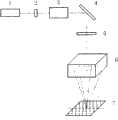
图1为本发明的采用激光干涉光刻技术的自清洁表面结构的制作系统示意图。FIG. 1 is a schematic diagram of a production system of a self-cleaning surface structure using laser interference lithography technology according to the present invention.
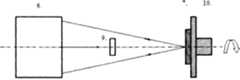
图2为二光束或三光束多次曝光方法示意图。Fig. 2 is a schematic diagram of a two-beam or three-beam multiple exposure method.
图3为用干涉图案结合扫描方式制作超大面积微纳自清洁表面结构的示意图。Fig. 3 is a schematic diagram of fabricating a super-large-area micro-nano self-cleaning surface structure by using an interference pattern combined with a scanning method.
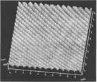
图4为四光束激光干涉纳米光刻获得的有序柱状阵列结构。Figure 4 shows the ordered columnar array structure obtained by four-beam laser interference nanolithography.
具体实施方式Detailed ways
如图1所示,本发明的采用激光干涉光刻技术的自清洁表面结构的制作系统包括激光器1,扩束镜2,准直系统3,反射镜4,偏振器件5,分束与折光系统6,基片7。由激光器1发出的激光束经扩束2和准直3后,被反射镜4折转光路,通过偏振器件5将光束变成线偏振光,再由分束与折光系统6先将激光束分成多个相干光束,再将多束光的各个光路分别控制,使它们以一定的入射角同时照射到基片7上,利用多束相干光干涉场内光强度强弱重新分布后的激光能量烧蚀材料表面,在大面积范围内产生微米或纳米级密集的柱形或锥形浮雕结构,形成自清洁表面结构。As shown in Figure 1, the fabrication system of the self-cleaning surface structure adopting laser interference lithography technology of the present invention comprises a
所述的分束与折光系统6中的分束功能可以由镀有分光膜的光学分光镜或者衍射光栅实现;折光即光路的转折,可利用光学反射镜实现。通过变换光学器件的相对摆放位置,改变照射到基片或其它材料表面的相干光束的入射角,从而调整自清洁表面的微细浮雕结构的参数,使其更有针对性,具有工作参数可控性好的优点。通过用线位移或角位移控制系统改变入射光夹角,实现系统的光刻特征尺寸可从几纳米到几百微米可调。The beam splitting function in the beam splitting and
也可以在光路中增加光学偏振器件,以提高干涉图形的对比度,从而提高表面微结构的制作效率和质量。An optical polarization device can also be added in the optical path to increase the contrast of the interference pattern, thereby improving the production efficiency and quality of the surface microstructure.
如图2所示,也可以使用二光束或者三光束干涉条纹图案辅助两次曝光基片材料表面,制成自清洁结构。经过分束与折光系统6出射的二光束或者三光束,对基片7曝光后,将吸附基片的工件台10或者将分束与折光系统6以预先设定的角度旋转,使干涉条纹图案与第一次曝光的图案成预先设定的角度,进行第二次曝光,利用两次干涉图案的强度叠加对基片材料表面进行烧蚀,以更简单灵活的方式产生预期的表面自清洁浮雕结构。移动挡板9挡住或放开三光束中的中间一束,即可在三光束和二光束之间转换。As shown in FIG. 2 , a two-beam or three-beam interference fringe pattern can also be used to assist in exposing the surface of the substrate material twice to form a self-cleaning structure. After the two or three beams emitted by the beam splitting and refracting
如图3所示,形成特定大面积自清洁结构的方法,也可以在满足光能量阈值允许范围的基础上扩束后,结合移动基片工件台10或者干涉光学系统6,用多光束干涉图案8扫描曝光基片7,形成超大面积微纳自清洁结构。As shown in Figure 3, the method of forming a specific large-area self-cleaning structure can also be combined with the moving substrate workpiece table 10 or the interference
形成特定高密度自清洁结构方法,除通过减小激光波长或增大入射光夹角实现外,还可通过光学移相或机械位移样品,然后重复曝光或多次曝光插补实现高密度微纳自清洁结构,所得结构如图3所示。The method of forming a specific high-density self-cleaning structure, in addition to reducing the laser wavelength or increasing the incident light angle, can also achieve high-density micro-nano by optical phase shifting or mechanical displacement of the sample, and then repeated exposure or multiple exposure interpolation Self-cleaning structure, the resulting structure is shown in Figure 3.
图4为利用图1所示的方案,通过四光束激光干涉光刻获得的有序纳米阵列结构,特征尺寸约200nm。FIG. 4 shows an ordered nano-array structure obtained by four-beam laser interference lithography using the scheme shown in FIG. 1 , with a characteristic size of about 200 nm.
Claims (8)
Priority Applications (1)
| Application Number | Priority Date | Filing Date | Title |
|---|---|---|---|
| CN201010101488ACN101844272A (en) | 2010-01-27 | 2010-01-27 | Method and system for manufacturing self-cleaning surface structure by adopting laser interference photoetching technology |
Applications Claiming Priority (1)
| Application Number | Priority Date | Filing Date | Title |
|---|---|---|---|
| CN201010101488ACN101844272A (en) | 2010-01-27 | 2010-01-27 | Method and system for manufacturing self-cleaning surface structure by adopting laser interference photoetching technology |
Publications (1)
| Publication Number | Publication Date |
|---|---|
| CN101844272Atrue CN101844272A (en) | 2010-09-29 |
Family
ID=42769184
Family Applications (1)
| Application Number | Title | Priority Date | Filing Date |
|---|---|---|---|
| CN201010101488APendingCN101844272A (en) | 2010-01-27 | 2010-01-27 | Method and system for manufacturing self-cleaning surface structure by adopting laser interference photoetching technology |
Country Status (1)
| Country | Link |
|---|---|
| CN (1) | CN101844272A (en) |
Cited By (25)
| Publication number | Priority date | Publication date | Assignee | Title |
|---|---|---|---|---|
| CN101980083A (en)* | 2010-09-13 | 2011-02-23 | 长春理工大学 | Method and system for fabricating filter membrane mesh structure by laser interference lithography |
| CN102581904A (en)* | 2012-02-08 | 2012-07-18 | 中南林业科技大学 | Method for processing self-cleaning solid wood floors by laser ablation |
| CN103320825A (en)* | 2013-06-06 | 2013-09-25 | 宁波微极电子科技有限公司 | Method for manufacturing high-density large-scale micro-nano-structure array |
| CN103663358A (en)* | 2012-09-20 | 2014-03-26 | 长春理工大学 | Method for preparing super-hydrophobic surface on silicon wafer based on laser interference nanometer lithography |
| TWI469762B (en)* | 2011-11-25 | 2015-01-21 | Ind Tech Res Inst | Electrosurgical unit with micro/nano structures and the manufacturing method thereof |
| CN104625415A (en)* | 2014-12-17 | 2015-05-20 | 中国航空工业集团公司北京航空制造工程研究所 | Method and device for preparing bionic super-hydrophobic micro-nano surface through femtosecond laser |
| CN104911519A (en)* | 2015-05-28 | 2015-09-16 | 湖北工业大学 | Method for preparing titanium alloy super-hydrophobic and anti-frost surface by using ultra-short pulse laser |
| CN104947016A (en)* | 2015-05-28 | 2015-09-30 | 湖北工业大学 | Method for preparing zinc alloy super-hydrophobic and self-cleaning surface by using ultra-short pulse laser |
| CN106141438A (en)* | 2015-04-03 | 2016-11-23 | 长春理工大学 | A kind of method utilizing laser plasma filament to prepare metal multifunction surface |
| CN107199404A (en)* | 2017-06-07 | 2017-09-26 | 湖北工业大学 | The optical chip array system of processing and method of ultrafast laser |
| CN107671078A (en)* | 2017-11-07 | 2018-02-09 | 英诺激光科技股份有限公司 | A kind of Handheld laser cleaning appts |
| CN109626317A (en)* | 2018-12-18 | 2019-04-16 | 哈尔滨工业大学 | A kind of composite construction film and preparation method thereof based on double gradient taper hole arrays |
| CN109634047A (en)* | 2019-01-28 | 2019-04-16 | 前海申升科技(深圳)有限公司 | A kind of eyeshield high definition photonic crystal image film |
| CN110854300A (en)* | 2019-11-27 | 2020-02-28 | 京东方科技集团股份有限公司 | Display device, display panel and manufacturing method thereof |
| CN110899983A (en)* | 2019-12-09 | 2020-03-24 | 沈阳理工大学 | Method for improving surface functionality of part by applying laser interference |
| CN110967945A (en)* | 2019-12-12 | 2020-04-07 | 卢欣霁 | System and method for manufacturing non-modulation array structure by laser interference lithography |
| CN111077734A (en)* | 2018-10-18 | 2020-04-28 | 中国科学院长春光学精密机械与物理研究所 | Method and system for manufacturing non-modulation array structure by adopting laser interference photoetching technology |
| CN111438438A (en)* | 2020-01-15 | 2020-07-24 | 华中科技大学 | A kind of laser high-efficiency large-area dynamic interference processing device and method |
| CN111774731A (en)* | 2020-06-24 | 2020-10-16 | 北京航空航天大学 | An ultrafast laser preparation method for antibacterial surfaces of public goods |
| CN111805089A (en)* | 2019-04-12 | 2020-10-23 | 湘潭大学 | A stable superhydrophobic self-cleaning surface and its preparation method by double-beam interferometry |
| CN112872591A (en)* | 2019-11-29 | 2021-06-01 | 中国科学技术大学 | System and method for quickly preparing high-length-diameter-ratio polymer microcolumn by femtosecond laser |
| CN113175867A (en)* | 2021-05-24 | 2021-07-27 | 浙江理工大学 | Sine phase modulation laser interferometer and carrier generation and signal demodulation method |
| CN113172347A (en)* | 2021-05-14 | 2021-07-27 | 江苏大学 | A composite textured metal ice-phobic surface and its processing method |
| CN113515020A (en)* | 2021-04-26 | 2021-10-19 | 长春理工大学 | Additive Manufacturing System |
| CN114160982A (en)* | 2021-12-06 | 2022-03-11 | 山西大学 | Processing system and processing method of laser speckle microstructure |
Citations (4)
| Publication number | Priority date | Publication date | Assignee | Title |
|---|---|---|---|---|
| JPH0547639A (en)* | 1991-08-09 | 1993-02-26 | Canon Inc | Illuminator and projection aligner using the same |
| CN1818798A (en)* | 2006-03-15 | 2006-08-16 | 浙江大学 | Method and device for producing photon crystal mask layer on LED |
| CN1821883A (en)* | 2006-01-12 | 2006-08-23 | 苏州大学 | Method and device for microstructure photoetching on smooth surface |
| CN1862353A (en)* | 2006-06-12 | 2006-11-15 | 江苏大学 | Method for making surface period minute structure and apparatus thereof |
- 2010
- 2010-01-27CNCN201010101488Apatent/CN101844272A/enactivePending
Patent Citations (4)
| Publication number | Priority date | Publication date | Assignee | Title |
|---|---|---|---|---|
| JPH0547639A (en)* | 1991-08-09 | 1993-02-26 | Canon Inc | Illuminator and projection aligner using the same |
| CN1821883A (en)* | 2006-01-12 | 2006-08-23 | 苏州大学 | Method and device for microstructure photoetching on smooth surface |
| CN1818798A (en)* | 2006-03-15 | 2006-08-16 | 浙江大学 | Method and device for producing photon crystal mask layer on LED |
| CN1862353A (en)* | 2006-06-12 | 2006-11-15 | 江苏大学 | Method for making surface period minute structure and apparatus thereof |
Non-Patent Citations (1)
| Title |
|---|
| 张锦: "用于大面积周期性图形制造的激光干涉光刻", 《光电工程》* |
Cited By (33)
| Publication number | Priority date | Publication date | Assignee | Title |
|---|---|---|---|---|
| CN101980083B (en)* | 2010-09-13 | 2013-02-20 | 长春理工大学 | Method for preparing filter membrane mesh structure by laser interference photoetching technology |
| CN101980083A (en)* | 2010-09-13 | 2011-02-23 | 长春理工大学 | Method and system for fabricating filter membrane mesh structure by laser interference lithography |
| TWI469762B (en)* | 2011-11-25 | 2015-01-21 | Ind Tech Res Inst | Electrosurgical unit with micro/nano structures and the manufacturing method thereof |
| CN102581904A (en)* | 2012-02-08 | 2012-07-18 | 中南林业科技大学 | Method for processing self-cleaning solid wood floors by laser ablation |
| CN103663358B (en)* | 2012-09-20 | 2016-11-23 | 长春理工大学 | The method preparing super hydrophobic surface on silicon chip based on laser interference nanometer lithography |
| CN103663358A (en)* | 2012-09-20 | 2014-03-26 | 长春理工大学 | Method for preparing super-hydrophobic surface on silicon wafer based on laser interference nanometer lithography |
| CN103320825B (en)* | 2013-06-06 | 2015-07-08 | 宁波微极电子科技有限公司 | Method for manufacturing high-density large-scale micro-nano structure array |
| CN103320825A (en)* | 2013-06-06 | 2013-09-25 | 宁波微极电子科技有限公司 | Method for manufacturing high-density large-scale micro-nano-structure array |
| CN104625415A (en)* | 2014-12-17 | 2015-05-20 | 中国航空工业集团公司北京航空制造工程研究所 | Method and device for preparing bionic super-hydrophobic micro-nano surface through femtosecond laser |
| CN104625415B (en)* | 2014-12-17 | 2016-06-08 | 中国航空工业集团公司北京航空制造工程研究所 | Femtosecond laser prepares method and the device of bionic super-hydrophobic micro nano surface |
| CN106141438A (en)* | 2015-04-03 | 2016-11-23 | 长春理工大学 | A kind of method utilizing laser plasma filament to prepare metal multifunction surface |
| CN104911519A (en)* | 2015-05-28 | 2015-09-16 | 湖北工业大学 | Method for preparing titanium alloy super-hydrophobic and anti-frost surface by using ultra-short pulse laser |
| CN104947016A (en)* | 2015-05-28 | 2015-09-30 | 湖北工业大学 | Method for preparing zinc alloy super-hydrophobic and self-cleaning surface by using ultra-short pulse laser |
| CN104911519B (en)* | 2015-05-28 | 2017-12-08 | 湖北工业大学 | A kind of method that titanium alloy super-hydrophobic frost resistance surface is prepared using ultra-short pulse laser |
| CN107199404A (en)* | 2017-06-07 | 2017-09-26 | 湖北工业大学 | The optical chip array system of processing and method of ultrafast laser |
| CN107671078A (en)* | 2017-11-07 | 2018-02-09 | 英诺激光科技股份有限公司 | A kind of Handheld laser cleaning appts |
| CN111077734A (en)* | 2018-10-18 | 2020-04-28 | 中国科学院长春光学精密机械与物理研究所 | Method and system for manufacturing non-modulation array structure by adopting laser interference photoetching technology |
| CN109626317A (en)* | 2018-12-18 | 2019-04-16 | 哈尔滨工业大学 | A kind of composite construction film and preparation method thereof based on double gradient taper hole arrays |
| CN109634047A (en)* | 2019-01-28 | 2019-04-16 | 前海申升科技(深圳)有限公司 | A kind of eyeshield high definition photonic crystal image film |
| CN111805089A (en)* | 2019-04-12 | 2020-10-23 | 湘潭大学 | A stable superhydrophobic self-cleaning surface and its preparation method by double-beam interferometry |
| CN110854300A (en)* | 2019-11-27 | 2020-02-28 | 京东方科技集团股份有限公司 | Display device, display panel and manufacturing method thereof |
| CN112872591B (en)* | 2019-11-29 | 2021-12-14 | 中国科学技术大学 | System and method for quickly preparing high-length-diameter-ratio polymer microcolumn by femtosecond laser |
| CN112872591A (en)* | 2019-11-29 | 2021-06-01 | 中国科学技术大学 | System and method for quickly preparing high-length-diameter-ratio polymer microcolumn by femtosecond laser |
| CN110899983A (en)* | 2019-12-09 | 2020-03-24 | 沈阳理工大学 | Method for improving surface functionality of part by applying laser interference |
| CN110967945A (en)* | 2019-12-12 | 2020-04-07 | 卢欣霁 | System and method for manufacturing non-modulation array structure by laser interference lithography |
| CN111438438A (en)* | 2020-01-15 | 2020-07-24 | 华中科技大学 | A kind of laser high-efficiency large-area dynamic interference processing device and method |
| CN111774731A (en)* | 2020-06-24 | 2020-10-16 | 北京航空航天大学 | An ultrafast laser preparation method for antibacterial surfaces of public goods |
| CN113515020A (en)* | 2021-04-26 | 2021-10-19 | 长春理工大学 | Additive Manufacturing System |
| CN113515020B (en)* | 2021-04-26 | 2022-11-11 | 长春理工大学 | Additive manufacturing system |
| CN113172347A (en)* | 2021-05-14 | 2021-07-27 | 江苏大学 | A composite textured metal ice-phobic surface and its processing method |
| CN113175867A (en)* | 2021-05-24 | 2021-07-27 | 浙江理工大学 | Sine phase modulation laser interferometer and carrier generation and signal demodulation method |
| CN113175867B (en)* | 2021-05-24 | 2022-07-26 | 浙江理工大学 | Sine phase modulation laser interferometer and carrier generation and signal demodulation method |
| CN114160982A (en)* | 2021-12-06 | 2022-03-11 | 山西大学 | Processing system and processing method of laser speckle microstructure |
Similar Documents
| Publication | Publication Date | Title |
|---|---|---|
| CN101844272A (en) | Method and system for manufacturing self-cleaning surface structure by adopting laser interference photoetching technology | |
| CN101924166B (en) | Manufacturing system and manufacturing method of solar cell surface antireflection structure | |
| KR101520196B1 (en) | Mask for near-field lithography and fabrication the same | |
| CN102269936B (en) | Method and system for simulating moth compound eye optical antireflection structure pattern | |
| US20030091752A1 (en) | Guided self-assembly of block copolymer films on interferometrically nanopatterned substrates | |
| US20130216779A1 (en) | Nanostructures from Laser-Ablated Nanohole Templates | |
| CN111805089A (en) | A stable superhydrophobic self-cleaning surface and its preparation method by double-beam interferometry | |
| Ali et al. | Review of laser nanomachining | |
| CN112162467A (en) | Laser curved surface processing system and manufacturing method for super-hydrophobic, anti-icing and wind resistance reduction | |
| CN113113289A (en) | Method for preparing silicon controlled nanowire by using femtosecond laser with remote/near field cooperative shaping | |
| Moronuki | Functional texture design and texturing processes | |
| CN108622848A (en) | A kind of three-dimensional composite nanostructure of large area and preparation method thereof | |
| Kang et al. | Photopatterning via photofluidization of azobenzene polymers | |
| Long et al. | Femtosecond laser processing for multi-functional hierarchical micro/nano structures on curved surfaces | |
| CN111366991A (en) | Optical metasurface, preparation method and processing device | |
| CN111999786A (en) | Hemispherical lens with opaque film covering spherical center and preparation method thereof | |
| CN101980083A (en) | Method and system for fabricating filter membrane mesh structure by laser interference lithography | |
| Amalathas et al. | Fabrication and Replication of Periodic Nanopyramid Structures by Laser Interference Lithography and UV | |
| Zhu et al. | Non-fully gold nanohole array fabricated by nanoimprint lithography | |
| Verma et al. | Taming of self-organization in highly confined soft matter to sub-100 nm scales: nanolens-arrays by spinodal instability of thin polymer films for high-resolution optical imaging | |
| Mao et al. | The fabrication of hydrophilic structure on lens via direct laser interference lithography | |
| CN111077734A (en) | Method and system for manufacturing non-modulation array structure by adopting laser interference photoetching technology | |
| Rajput et al. | Polymer-based Soft Topographical Features Functionalized by Magnetron Sputtering | |
| Xing et al. | Fabrication of Biomimetic Surface for Hydrophobic and Anti-icing Purposes via the Capillary Force Lithography | |
| CN110967945A (en) | System and method for manufacturing non-modulation array structure by laser interference lithography |
Legal Events
| Date | Code | Title | Description |
|---|---|---|---|
| C06 | Publication | ||
| PB01 | Publication | ||
| C10 | Entry into substantive examination | ||
| SE01 | Entry into force of request for substantive examination | ||
| C02 | Deemed withdrawal of patent application after publication (patent law 2001) | ||
| WD01 | Invention patent application deemed withdrawn after publication | Application publication date:20100929 |