CN101840863A - Semiconductor device and method for manufacturing semiconductor device - Google Patents
Semiconductor device and method for manufacturing semiconductor deviceDownload PDFInfo
- Publication number
- CN101840863A CN101840863ACN201010138337.0ACN201010138337ACN101840863ACN 101840863 ACN101840863 ACN 101840863ACN 201010138337 ACN201010138337 ACN 201010138337ACN 101840863 ACN101840863 ACN 101840863A
- Authority
- CN
- China
- Prior art keywords
- layer
- semiconductor
- germanium
- oxide
- dielectric layer
- Prior art date
- Legal status (The legal status is an assumption and is not a legal conclusion. Google has not performed a legal analysis and makes no representation as to the accuracy of the status listed.)
- Granted
Links
- 239000004065semiconductorSubstances0.000titleclaimsabstractdescription108
- 238000000034methodMethods0.000titleclaimsabstractdescription43
- 238000004519manufacturing processMethods0.000titleclaimsabstractdescription26
- 239000000758substrateSubstances0.000claimsabstractdescription60
- 229910044991metal oxideInorganic materials0.000claimsabstractdescription16
- 150000004706metal oxidesChemical class0.000claimsabstractdescription15
- GNPVGFCGXDBREM-UHFFFAOYSA-Ngermanium atomChemical group[Ge]GNPVGFCGXDBREM-UHFFFAOYSA-N0.000claimsdescription67
- 229910052732germaniumInorganic materials0.000claimsdescription64
- 239000000463materialSubstances0.000claimsdescription49
- 229910052751metalInorganic materials0.000claimsdescription46
- 239000002184metalSubstances0.000claimsdescription46
- YBMRDBCBODYGJE-UHFFFAOYSA-Ngermanium oxideInorganic materialsO=[Ge]=OYBMRDBCBODYGJE-UHFFFAOYSA-N0.000claimsdescription33
- MCMNRKCIXSYSNV-UHFFFAOYSA-NZrO2Inorganic materialsO=[Zr]=OMCMNRKCIXSYSNV-UHFFFAOYSA-N0.000claimsdescription18
- PVADDRMAFCOOPC-UHFFFAOYSA-NoxogermaniumChemical compound[Ge]=OPVADDRMAFCOOPC-UHFFFAOYSA-N0.000claimsdescription17
- 239000012212insulatorSubstances0.000claimsdescription15
- -1hafnium nitrideChemical class0.000claimsdescription14
- 150000004767nitridesChemical class0.000claimsdescription14
- 229910052735hafniumInorganic materials0.000claimsdescription13
- QVGXLLKOCUKJST-UHFFFAOYSA-Natomic oxygenChemical compound[O]QVGXLLKOCUKJST-UHFFFAOYSA-N0.000claimsdescription12
- 238000000151depositionMethods0.000claimsdescription12
- 229910052782aluminiumInorganic materials0.000claimsdescription11
- XAGFODPZIPBFFR-UHFFFAOYSA-NaluminiumChemical compound[Al]XAGFODPZIPBFFR-UHFFFAOYSA-N0.000claimsdescription11
- 239000001301oxygenSubstances0.000claimsdescription11
- 229910052760oxygenInorganic materials0.000claimsdescription11
- 239000010936titaniumSubstances0.000claimsdescription11
- YCKRFDGAMUMZLT-UHFFFAOYSA-NFluorine atomChemical compound[F]YCKRFDGAMUMZLT-UHFFFAOYSA-N0.000claimsdescription10
- 239000003990capacitorSubstances0.000claimsdescription10
- 230000005669field effectEffects0.000claimsdescription10
- 229910052731fluorineInorganic materials0.000claimsdescription10
- 239000011737fluorineSubstances0.000claimsdescription10
- RTAQQCXQSZGOHL-UHFFFAOYSA-NTitaniumChemical compound[Ti]RTAQQCXQSZGOHL-UHFFFAOYSA-N0.000claimsdescription9
- 229910052719titaniumInorganic materials0.000claimsdescription9
- VBJZVLUMGGDVMO-UHFFFAOYSA-Nhafnium atomChemical compound[Hf]VBJZVLUMGGDVMO-UHFFFAOYSA-N0.000claimsdescription8
- 229910052715tantalumInorganic materials0.000claimsdescription7
- GUVRBAGPIYLISA-UHFFFAOYSA-Ntantalum atomChemical compound[Ta]GUVRBAGPIYLISA-UHFFFAOYSA-N0.000claimsdescription7
- NRTOMJZYCJJWKI-UHFFFAOYSA-NTitanium nitrideChemical compound[Ti]#NNRTOMJZYCJJWKI-UHFFFAOYSA-N0.000claimsdescription6
- QCWXUUIWCKQGHC-UHFFFAOYSA-NZirconiumChemical compound[Zr]QCWXUUIWCKQGHC-UHFFFAOYSA-N0.000claimsdescription6
- 238000000137annealingMethods0.000claimsdescription6
- 229910052746lanthanumInorganic materials0.000claimsdescription6
- FZLIPJUXYLNCLC-UHFFFAOYSA-Nlanthanum atomChemical compound[La]FZLIPJUXYLNCLC-UHFFFAOYSA-N0.000claimsdescription6
- 239000002243precursorSubstances0.000claimsdescription6
- WFKWXMTUELFFGS-UHFFFAOYSA-NtungstenChemical compound[W]WFKWXMTUELFFGS-UHFFFAOYSA-N0.000claimsdescription6
- 229910052721tungstenInorganic materials0.000claimsdescription6
- 239000010937tungstenSubstances0.000claimsdescription6
- 229910052726zirconiumInorganic materials0.000claimsdescription6
- 150000001875compoundsChemical class0.000claimsdescription5
- MRELNEQAGSRDBK-UHFFFAOYSA-Nlanthanum(3+);oxygen(2-)Chemical compound[O-2].[O-2].[O-2].[La+3].[La+3]MRELNEQAGSRDBK-UHFFFAOYSA-N0.000claimsdescription5
- TWNQGVIAIRXVLR-UHFFFAOYSA-Noxo(oxoalumanyloxy)alumaneChemical compoundO=[Al]O[Al]=OTWNQGVIAIRXVLR-UHFFFAOYSA-N0.000claimsdescription5
- BPUBBGLMJRNUCC-UHFFFAOYSA-Noxygen(2-);tantalum(5+)Chemical compound[O-2].[O-2].[O-2].[O-2].[O-2].[Ta+5].[Ta+5]BPUBBGLMJRNUCC-UHFFFAOYSA-N0.000claimsdescription5
- YAIQCYZCSGLAAN-UHFFFAOYSA-N[Si+4].[O-2].[Al+3]Chemical compound[Si+4].[O-2].[Al+3]YAIQCYZCSGLAAN-UHFFFAOYSA-N0.000claimsdescription4
- GPBUGPUPKAGMDK-UHFFFAOYSA-NazanylidynemolybdenumChemical compound[Mo]#NGPBUGPUPKAGMDK-UHFFFAOYSA-N0.000claimsdescription4
- CJNBYAVZURUTKZ-UHFFFAOYSA-Nhafnium(iv) oxideChemical compoundO=[Hf]=OCJNBYAVZURUTKZ-UHFFFAOYSA-N0.000claimsdescription4
- MZLGASXMSKOWSE-UHFFFAOYSA-Ntantalum nitrideChemical compound[Ta]#NMZLGASXMSKOWSE-UHFFFAOYSA-N0.000claimsdescription4
- GWEVSGVZZGPLCZ-UHFFFAOYSA-NTitan oxideChemical compoundO=[Ti]=OGWEVSGVZZGPLCZ-UHFFFAOYSA-N0.000claimsdescription3
- XIGWMASYASFMFN-UHFFFAOYSA-N[Si+4].[O-2].[Al+3].[Hf+4]Chemical compound[Si+4].[O-2].[Al+3].[Hf+4]XIGWMASYASFMFN-UHFFFAOYSA-N0.000claimsdescription3
- MIQVEZFSDIJTMW-UHFFFAOYSA-Naluminum hafnium(4+) oxygen(2-)Chemical compound[O-2].[Al+3].[Hf+4]MIQVEZFSDIJTMW-UHFFFAOYSA-N0.000claimsdescription3
- RVTZCBVAJQQJTK-UHFFFAOYSA-Noxygen(2-);zirconium(4+)Chemical compound[O-2].[O-2].[Zr+4]RVTZCBVAJQQJTK-UHFFFAOYSA-N0.000claimsdescription3
- ILCYGSITMBHYNK-UHFFFAOYSA-N[Si]=O.[Hf]Chemical compound[Si]=O.[Hf]ILCYGSITMBHYNK-UHFFFAOYSA-N0.000claimsdescription2
- PBCFLUZVCVVTBY-UHFFFAOYSA-Ntantalum pentoxideInorganic materialsO=[Ta](=O)O[Ta](=O)=OPBCFLUZVCVVTBY-UHFFFAOYSA-N0.000claimsdescription2
- JBXGTIPBTJVLDK-UHFFFAOYSA-N[O-2].[Al+3].[Ge+2]Chemical compound[O-2].[Al+3].[Ge+2]JBXGTIPBTJVLDK-UHFFFAOYSA-N0.000claims2
- MOGRQVOVCATFGE-UHFFFAOYSA-N[Ge]=O.[Hf]Chemical compound[Ge]=O.[Hf]MOGRQVOVCATFGE-UHFFFAOYSA-N0.000claims1
- UQZIWOQVLUASCR-UHFFFAOYSA-Nalumane;titaniumChemical compound[AlH3].[Ti]UQZIWOQVLUASCR-UHFFFAOYSA-N0.000claims1
- VIJYFGMFEVJQHU-UHFFFAOYSA-Naluminum oxosilicon(2+) oxygen(2-)Chemical compound[O-2].[Al+3].[Si+2]=OVIJYFGMFEVJQHU-UHFFFAOYSA-N0.000claims1
- GEZAXHSNIQTPMM-UHFFFAOYSA-Ndysprosium(3+);oxygen(2-)Chemical compound[O-2].[O-2].[O-2].[Dy+3].[Dy+3]GEZAXHSNIQTPMM-UHFFFAOYSA-N0.000claims1
- RUDFQVOCFDJEEF-UHFFFAOYSA-Noxygen(2-);yttrium(3+)Chemical compound[O-2].[O-2].[O-2].[Y+3].[Y+3]RUDFQVOCFDJEEF-UHFFFAOYSA-N0.000claims1
- UVGLBOPDEUYYCS-UHFFFAOYSA-Nsilicon zirconiumChemical compound[Si].[Zr]UVGLBOPDEUYYCS-UHFFFAOYSA-N0.000claims1
- 239000004408titanium dioxideSubstances0.000claims1
- 239000010410layerSubstances0.000description203
- XUIMIQQOPSSXEZ-UHFFFAOYSA-NSiliconChemical compound[Si]XUIMIQQOPSSXEZ-UHFFFAOYSA-N0.000description21
- 229910052710siliconInorganic materials0.000description21
- 239000010703siliconSubstances0.000description21
- 230000008569processEffects0.000description19
- 239000003989dielectric materialSubstances0.000description14
- 238000002955isolationMethods0.000description11
- 125000006850spacer groupChemical group0.000description11
- 230000007547defectEffects0.000description10
- 239000000203mixtureSubstances0.000description10
- 230000000087stabilizing effectEffects0.000description10
- 238000005229chemical vapour depositionMethods0.000description9
- 238000000231atomic layer depositionMethods0.000description8
- 229940119177germanium dioxideDrugs0.000description8
- 125000005843halogen groupChemical group0.000description8
- 239000007943implantSubstances0.000description8
- 230000003647oxidationEffects0.000description8
- 238000007254oxidation reactionMethods0.000description8
- 125000004429atomChemical group0.000description7
- SCCCLDWUZODEKG-UHFFFAOYSA-NgermanideChemical compound[GeH3-]SCCCLDWUZODEKG-UHFFFAOYSA-N0.000description6
- 230000037230mobilityEffects0.000description6
- PXHVJJICTQNCMI-UHFFFAOYSA-NNickelChemical compound[Ni]PXHVJJICTQNCMI-UHFFFAOYSA-N0.000description5
- CBENFWSGALASAD-UHFFFAOYSA-NOzoneChemical compound[O-][O+]=OCBENFWSGALASAD-UHFFFAOYSA-N0.000description5
- 238000000026X-ray photoelectron spectrumMethods0.000description5
- 230000008901benefitEffects0.000description5
- 230000015572biosynthetic processEffects0.000description5
- 150000002739metalsChemical class0.000description5
- QKCGXXHCELUCKW-UHFFFAOYSA-Nn-[4-[4-(dinaphthalen-2-ylamino)phenyl]phenyl]-n-naphthalen-2-ylnaphthalen-2-amineChemical compoundC1=CC=CC2=CC(N(C=3C=CC(=CC=3)C=3C=CC(=CC=3)N(C=3C=C4C=CC=CC4=CC=3)C=3C=C4C=CC=CC4=CC=3)C3=CC4=CC=CC=C4C=C3)=CC=C21QKCGXXHCELUCKW-UHFFFAOYSA-N0.000description5
- 238000005240physical vapour depositionMethods0.000description5
- BASFCYQUMIYNBI-UHFFFAOYSA-NplatinumChemical compound[Pt]BASFCYQUMIYNBI-UHFFFAOYSA-N0.000description5
- 229910021332silicideInorganic materials0.000description5
- FVBUAEGBCNSCDD-UHFFFAOYSA-Nsilicide(4-)Chemical compound[Si-4]FVBUAEGBCNSCDD-UHFFFAOYSA-N0.000description5
- 229910005793GeO 2Inorganic materials0.000description4
- 229910052581Si3N4Inorganic materials0.000description4
- 230000008859changeEffects0.000description4
- 239000004020conductorSubstances0.000description4
- 229910021420polycrystalline siliconInorganic materials0.000description4
- 229920005591polysiliconPolymers0.000description4
- JBRZTFJDHDCESZ-UHFFFAOYSA-NAsGaChemical compound[As]#[Ga]JBRZTFJDHDCESZ-UHFFFAOYSA-N0.000description3
- 229910001218Gallium arsenideInorganic materials0.000description3
- 229910003855HfAlOInorganic materials0.000description3
- KDLHZDBZIXYQEI-UHFFFAOYSA-NPalladiumChemical compound[Pd]KDLHZDBZIXYQEI-UHFFFAOYSA-N0.000description3
- VYPSYNLAJGMNEJ-UHFFFAOYSA-NSilicium dioxideChemical compoundO=[Si]=OVYPSYNLAJGMNEJ-UHFFFAOYSA-N0.000description3
- 230000005527interface trapEffects0.000description3
- 239000002356single layerSubstances0.000description3
- 238000007740vapor depositionMethods0.000description3
- 229910018072Al 2 O 3Inorganic materials0.000description2
- IJGRMHOSHXDMSA-UHFFFAOYSA-NAtomic nitrogenChemical compoundN#NIJGRMHOSHXDMSA-UHFFFAOYSA-N0.000description2
- 229910052688GadoliniumInorganic materials0.000description2
- 229910004129HfSiOInorganic materials0.000description2
- GPXJNWSHGFTCBW-UHFFFAOYSA-NIndium phosphideChemical compound[In]#PGPXJNWSHGFTCBW-UHFFFAOYSA-N0.000description2
- 238000004833X-ray photoelectron spectroscopyMethods0.000description2
- 229910007875ZrAlOInorganic materials0.000description2
- 229910006501ZrSiOInorganic materials0.000description2
- YYXJRCXTIUJJMP-UHFFFAOYSA-Naluminum;gadolinium(3+);oxygen(2-)Chemical compound[O-2].[O-2].[O-2].[Al+3].[Gd+3]YYXJRCXTIUJJMP-UHFFFAOYSA-N0.000description2
- UIWYJDYFSGRHKR-UHFFFAOYSA-Ngadolinium atomChemical compound[Gd]UIWYJDYFSGRHKR-UHFFFAOYSA-N0.000description2
- 239000007789gasSubstances0.000description2
- 238000001912gas jet depositionMethods0.000description2
- 238000002513implantationMethods0.000description2
- 239000011810insulating materialSubstances0.000description2
- 230000010354integrationEffects0.000description2
- 150000002500ionsChemical class0.000description2
- 239000000395magnesium oxideSubstances0.000description2
- CPLXHLVBOLITMK-UHFFFAOYSA-Nmagnesium oxideInorganic materials[Mg]=OCPLXHLVBOLITMK-UHFFFAOYSA-N0.000description2
- QENHCSSJTJWZAL-UHFFFAOYSA-Nmagnesium sulfideChemical compound[Mg+2].[S-2]QENHCSSJTJWZAL-UHFFFAOYSA-N0.000description2
- AXZKOIWUVFPNLO-UHFFFAOYSA-Nmagnesium;oxygen(2-)Chemical compound[O-2].[Mg+2]AXZKOIWUVFPNLO-UHFFFAOYSA-N0.000description2
- NFFIWVVINABMKP-UHFFFAOYSA-NmethylidynetantalumChemical compound[Ta]#CNFFIWVVINABMKP-UHFFFAOYSA-N0.000description2
- 229910052759nickelInorganic materials0.000description2
- RUFLMLWJRZAWLJ-UHFFFAOYSA-Nnickel silicideChemical compound[Ni]=[Si]=[Ni]RUFLMLWJRZAWLJ-UHFFFAOYSA-N0.000description2
- 229910021334nickel silicideInorganic materials0.000description2
- 229910052697platinumInorganic materials0.000description2
- UUWCBFKLGFQDME-UHFFFAOYSA-Nplatinum titaniumChemical compound[Ti].[Pt]UUWCBFKLGFQDME-UHFFFAOYSA-N0.000description2
- 239000010948rhodiumSubstances0.000description2
- LIVNPJMFVYWSIS-UHFFFAOYSA-Nsilicon monoxideChemical compound[Si-]#[O+]LIVNPJMFVYWSIS-UHFFFAOYSA-N0.000description2
- HQVNEWCFYHHQES-UHFFFAOYSA-Nsilicon nitrideChemical compoundN12[Si]34N5[Si]62N3[Si]51N64HQVNEWCFYHHQES-UHFFFAOYSA-N0.000description2
- 229910003468tantalcarbideInorganic materials0.000description2
- 229910001936tantalum oxideInorganic materials0.000description2
- MTPVUVINMAGMJL-UHFFFAOYSA-Ntrimethyl(1,1,2,2,2-pentafluoroethyl)silaneChemical compoundC[Si](C)(C)C(F)(F)C(F)(F)FMTPVUVINMAGMJL-UHFFFAOYSA-N0.000description2
- ZVWKZXLXHLZXLS-UHFFFAOYSA-Nzirconium nitrideChemical compound[Zr]#NZVWKZXLXHLZXLS-UHFFFAOYSA-N0.000description2
- GFQYVLUOOAAOGM-UHFFFAOYSA-Nzirconium(iv) silicateChemical compound[Zr+4].[O-][Si]([O-])([O-])[O-]GFQYVLUOOAAOGM-UHFFFAOYSA-N0.000description2
- ZXEYZECDXFPJRJ-UHFFFAOYSA-N$l^{3}-silane;platinumChemical compound[SiH3].[Pt]ZXEYZECDXFPJRJ-UHFFFAOYSA-N0.000description1
- MYMOFIZGZYHOMD-UHFFFAOYSA-NDioxygenChemical compoundO=OMYMOFIZGZYHOMD-UHFFFAOYSA-N0.000description1
- 229910052691ErbiumInorganic materials0.000description1
- UFHFLCQGNIYNRP-UHFFFAOYSA-NHydrogenChemical compound[H][H]UFHFLCQGNIYNRP-UHFFFAOYSA-N0.000description1
- 229910021193La 2 O 3Inorganic materials0.000description1
- ZOKXTWBITQBERF-UHFFFAOYSA-NMolybdenumChemical compound[Mo]ZOKXTWBITQBERF-UHFFFAOYSA-N0.000description1
- 229910005889NiSixInorganic materials0.000description1
- BPQQTUXANYXVAA-UHFFFAOYSA-NOrthosilicateChemical compound[O-][Si]([O-])([O-])[O-]BPQQTUXANYXVAA-UHFFFAOYSA-N0.000description1
- 229910052777PraseodymiumInorganic materials0.000description1
- 235000003976RutaNutrition0.000description1
- 240000005746Ruta graveolensSpecies0.000description1
- 229910052769YtterbiumInorganic materials0.000description1
- YKTSYUJCYHOUJP-UHFFFAOYSA-N[O--].[Al+3].[Al+3].[O-][Si]([O-])([O-])[O-]Chemical compound[O--].[Al+3].[Al+3].[O-][Si]([O-])([O-])[O-]YKTSYUJCYHOUJP-UHFFFAOYSA-N0.000description1
- YJKVZNGTVPOCJV-UHFFFAOYSA-N[Rb].[Ta]Chemical compound[Rb].[Ta]YJKVZNGTVPOCJV-UHFFFAOYSA-N0.000description1
- CEPICIBPGDWCRU-UHFFFAOYSA-N[Si].[Hf]Chemical compound[Si].[Hf]CEPICIBPGDWCRU-UHFFFAOYSA-N0.000description1
- VYBYZVVRYQDCGQ-UHFFFAOYSA-Nalumane;hafniumChemical compound[AlH3].[Hf]VYBYZVVRYQDCGQ-UHFFFAOYSA-N0.000description1
- DNXNYEBMOSARMM-UHFFFAOYSA-Nalumane;zirconiumChemical compound[AlH3].[Zr]DNXNYEBMOSARMM-UHFFFAOYSA-N0.000description1
- CSDREXVUYHZDNP-UHFFFAOYSA-NalumanylidynesiliconChemical compound[Al].[Si]CSDREXVUYHZDNP-UHFFFAOYSA-N0.000description1
- IVHJCRXBQPGLOV-UHFFFAOYSA-NazanylidynetungstenChemical compound[W]#NIVHJCRXBQPGLOV-UHFFFAOYSA-N0.000description1
- SKKMWRVAJNPLFY-UHFFFAOYSA-NazanylidynevanadiumChemical compound[V]#NSKKMWRVAJNPLFY-UHFFFAOYSA-N0.000description1
- 230000009286beneficial effectEffects0.000description1
- 230000000903blocking effectEffects0.000description1
- 230000015556catabolic processEffects0.000description1
- 238000009614chemical analysis methodMethods0.000description1
- 229910017052cobaltInorganic materials0.000description1
- 239000010941cobaltSubstances0.000description1
- GUTLYIVDDKVIGB-UHFFFAOYSA-Ncobalt atomChemical compound[Co]GUTLYIVDDKVIGB-UHFFFAOYSA-N0.000description1
- DDHRUTNUHBNAHW-UHFFFAOYSA-Ncobalt germaniumChemical compound[Co].[Ge]DDHRUTNUHBNAHW-UHFFFAOYSA-N0.000description1
- 238000010276constructionMethods0.000description1
- 239000013078crystalSubstances0.000description1
- 230000002950deficientEffects0.000description1
- 238000006731degradation reactionMethods0.000description1
- 230000000593degrading effectEffects0.000description1
- 230000008021depositionEffects0.000description1
- 238000010586diagramMethods0.000description1
- 229910001882dioxygenInorganic materials0.000description1
- 238000009826distributionMethods0.000description1
- 239000002019doping agentSubstances0.000description1
- 229910003440dysprosium oxideInorganic materials0.000description1
- NLQFUUYNQFMIJW-UHFFFAOYSA-Ndysprosium(iii) oxideChemical compoundO=[Dy]O[Dy]=ONLQFUUYNQFMIJW-UHFFFAOYSA-N0.000description1
- 230000000694effectsEffects0.000description1
- 239000007772electrode materialSubstances0.000description1
- 230000007613environmental effectEffects0.000description1
- UYAHIZSMUZPPFV-UHFFFAOYSA-NerbiumChemical compound[Er]UYAHIZSMUZPPFV-UHFFFAOYSA-N0.000description1
- 239000010408filmSubstances0.000description1
- 229910001938gadolinium oxideInorganic materials0.000description1
- 229940075613gadolinium oxideDrugs0.000description1
- CMIHHWBVHJVIGI-UHFFFAOYSA-Ngadolinium(iii) oxideChemical compound[O-2].[O-2].[O-2].[Gd+3].[Gd+3]CMIHHWBVHJVIGI-UHFFFAOYSA-N0.000description1
- 150000002290germaniumChemical class0.000description1
- BIXHRBFZLLFBFL-UHFFFAOYSA-Ngermanium nitrideChemical compoundN#[Ge]N([Ge]#N)[Ge]#NBIXHRBFZLLFBFL-UHFFFAOYSA-N0.000description1
- INIGCWGJTZDVRY-UHFFFAOYSA-Nhafnium zirconiumChemical compound[Zr].[Hf]INIGCWGJTZDVRY-UHFFFAOYSA-N0.000description1
- 238000010438heat treatmentMethods0.000description1
- 239000001257hydrogenSubstances0.000description1
- 229910052739hydrogenInorganic materials0.000description1
- 238000009413insulationMethods0.000description1
- 238000005468ion implantationMethods0.000description1
- 229910052741iridiumInorganic materials0.000description1
- GKOZUEZYRPOHIO-UHFFFAOYSA-Niridium atomChemical compound[Ir]GKOZUEZYRPOHIO-UHFFFAOYSA-N0.000description1
- 229910052914metal silicateInorganic materials0.000description1
- 229910052750molybdenumInorganic materials0.000description1
- 239000011733molybdenumSubstances0.000description1
- 229910021421monocrystalline siliconInorganic materials0.000description1
- 229910052757nitrogenInorganic materials0.000description1
- 230000001590oxidative effectEffects0.000description1
- KJXBRHIPHIVJCS-UHFFFAOYSA-Noxo(oxoalumanyloxy)lanthanumChemical compoundO=[Al]O[La]=OKJXBRHIPHIVJCS-UHFFFAOYSA-N0.000description1
- SIWVEOZUMHYXCS-UHFFFAOYSA-Noxo(oxoyttriooxy)yttriumChemical compoundO=[Y]O[Y]=OSIWVEOZUMHYXCS-UHFFFAOYSA-N0.000description1
- 125000004430oxygen atomChemical groupO*0.000description1
- 229910052763palladiumInorganic materials0.000description1
- 238000002161passivationMethods0.000description1
- 238000000206photolithographyMethods0.000description1
- 229910021339platinum silicideInorganic materials0.000description1
- PUDIUYLPXJFUGB-UHFFFAOYSA-Npraseodymium atomChemical compound[Pr]PUDIUYLPXJFUGB-UHFFFAOYSA-N0.000description1
- 230000009467reductionEffects0.000description1
- 230000008439repair processEffects0.000description1
- 229910052702rheniumInorganic materials0.000description1
- WUAPFZMCVAUBPE-UHFFFAOYSA-Nrhenium atomChemical compound[Re]WUAPFZMCVAUBPE-UHFFFAOYSA-N0.000description1
- 229910052703rhodiumInorganic materials0.000description1
- MHOVAHRLVXNVSD-UHFFFAOYSA-Nrhodium atomChemical compound[Rh]MHOVAHRLVXNVSD-UHFFFAOYSA-N0.000description1
- 229910052701rubidiumInorganic materials0.000description1
- IGLNJRXAVVLDKE-UHFFFAOYSA-Nrubidium atomChemical compound[Rb]IGLNJRXAVVLDKE-UHFFFAOYSA-N0.000description1
- 235000005806rutaNutrition0.000description1
- VSZWPYCFIRKVQL-UHFFFAOYSA-Nselanylidenegallium;seleniumChemical compound[Se].[Se]=[Ga].[Se]=[Ga]VSZWPYCFIRKVQL-UHFFFAOYSA-N0.000description1
- 239000000377silicon dioxideSubstances0.000description1
- 235000012239silicon dioxideNutrition0.000description1
- 229910052814silicon oxideInorganic materials0.000description1
- HWEYZGSCHQNNEH-UHFFFAOYSA-Nsilicon tantalumChemical compound[Si].[Ta]HWEYZGSCHQNNEH-UHFFFAOYSA-N0.000description1
- 239000007921spraySubstances0.000description1
- 239000003381stabilizerSubstances0.000description1
- 239000000126substanceSubstances0.000description1
- 238000006467substitution reactionMethods0.000description1
- 239000002344surface layerSubstances0.000description1
- 239000010409thin filmSubstances0.000description1
- 229910021341titanium silicideInorganic materials0.000description1
- MAKDTFFYCIMFQP-UHFFFAOYSA-Ntitanium tungstenChemical compound[Ti].[W]MAKDTFFYCIMFQP-UHFFFAOYSA-N0.000description1
- 238000003949trap density measurementMethods0.000description1
- 230000005641tunnelingEffects0.000description1
- 239000002699waste materialSubstances0.000description1
- NAWDYIZEMPQZHO-UHFFFAOYSA-NytterbiumChemical compound[Yb]NAWDYIZEMPQZHO-UHFFFAOYSA-N0.000description1
- 229910052727yttriumInorganic materials0.000description1
- VWQVUPCCIRVNHF-UHFFFAOYSA-Nyttrium atomChemical compound[Y]VWQVUPCCIRVNHF-UHFFFAOYSA-N0.000description1
- 229910001928zirconium oxideInorganic materials0.000description1
Images


Classifications
- H—ELECTRICITY
- H10—SEMICONDUCTOR DEVICES; ELECTRIC SOLID-STATE DEVICES NOT OTHERWISE PROVIDED FOR
- H10D—INORGANIC ELECTRIC SEMICONDUCTOR DEVICES
- H10D30/00—Field-effect transistors [FET]
- H10D30/60—Insulated-gate field-effect transistors [IGFET]
- H10D30/601—Insulated-gate field-effect transistors [IGFET] having lightly-doped drain or source extensions, e.g. LDD IGFETs or DDD IGFETs
- H—ELECTRICITY
- H01—ELECTRIC ELEMENTS
- H01L—SEMICONDUCTOR DEVICES NOT COVERED BY CLASS H10
- H01L21/00—Processes or apparatus adapted for the manufacture or treatment of semiconductor or solid state devices or of parts thereof
- H01L21/02—Manufacture or treatment of semiconductor devices or of parts thereof
- H01L21/02104—Forming layers
- H01L21/02107—Forming insulating materials on a substrate
- H01L21/02109—Forming insulating materials on a substrate characterised by the type of layer, e.g. type of material, porous/non-porous, pre-cursors, mixtures or laminates
- H01L21/02112—Forming insulating materials on a substrate characterised by the type of layer, e.g. type of material, porous/non-porous, pre-cursors, mixtures or laminates characterised by the material of the layer
- H01L21/02172—Forming insulating materials on a substrate characterised by the type of layer, e.g. type of material, porous/non-porous, pre-cursors, mixtures or laminates characterised by the material of the layer the material containing at least one metal element, e.g. metal oxides, metal nitrides, metal oxynitrides or metal carbides
- H01L21/02175—Forming insulating materials on a substrate characterised by the type of layer, e.g. type of material, porous/non-porous, pre-cursors, mixtures or laminates characterised by the material of the layer the material containing at least one metal element, e.g. metal oxides, metal nitrides, metal oxynitrides or metal carbides characterised by the metal
- H—ELECTRICITY
- H01—ELECTRIC ELEMENTS
- H01L—SEMICONDUCTOR DEVICES NOT COVERED BY CLASS H10
- H01L21/00—Processes or apparatus adapted for the manufacture or treatment of semiconductor or solid state devices or of parts thereof
- H01L21/02—Manufacture or treatment of semiconductor devices or of parts thereof
- H01L21/04—Manufacture or treatment of semiconductor devices or of parts thereof the devices having potential barriers, e.g. a PN junction, depletion layer or carrier concentration layer
- H01L21/18—Manufacture or treatment of semiconductor devices or of parts thereof the devices having potential barriers, e.g. a PN junction, depletion layer or carrier concentration layer the devices having semiconductor bodies comprising elements of Group IV of the Periodic Table or AIIIBV compounds with or without impurities, e.g. doping materials
- H01L21/28—Manufacture of electrodes on semiconductor bodies using processes or apparatus not provided for in groups H01L21/20 - H01L21/268
- H01L21/28008—Making conductor-insulator-semiconductor electrodes
- H01L21/28255—Making conductor-insulator-semiconductor electrodes the insulator being formed after the semiconductor body, the semiconductor belonging to Group IV and not being elemental silicon, e.g. Ge, SiGe, SiGeC
- H—ELECTRICITY
- H10—SEMICONDUCTOR DEVICES; ELECTRIC SOLID-STATE DEVICES NOT OTHERWISE PROVIDED FOR
- H10D—INORGANIC ELECTRIC SEMICONDUCTOR DEVICES
- H10D30/00—Field-effect transistors [FET]
- H10D30/01—Manufacture or treatment
- H10D30/021—Manufacture or treatment of FETs having insulated gates [IGFET]
- H10D30/0223—Manufacture or treatment of FETs having insulated gates [IGFET] having source and drain regions or source and drain extensions self-aligned to sides of the gate
- H10D30/0227—Manufacture or treatment of FETs having insulated gates [IGFET] having source and drain regions or source and drain extensions self-aligned to sides of the gate having both lightly-doped source and drain extensions and source and drain regions self-aligned to the sides of the gate, e.g. lightly-doped drain [LDD] MOSFET or double-diffused drain [DDD] MOSFET
- H—ELECTRICITY
- H10—SEMICONDUCTOR DEVICES; ELECTRIC SOLID-STATE DEVICES NOT OTHERWISE PROVIDED FOR
- H10D—INORGANIC ELECTRIC SEMICONDUCTOR DEVICES
- H10D62/00—Semiconductor bodies, or regions thereof, of devices having potential barriers
- H10D62/80—Semiconductor bodies, or regions thereof, of devices having potential barriers characterised by the materials
- H10D62/83—Semiconductor bodies, or regions thereof, of devices having potential barriers characterised by the materials being Group IV materials, e.g. B-doped Si or undoped Ge
- H—ELECTRICITY
- H10—SEMICONDUCTOR DEVICES; ELECTRIC SOLID-STATE DEVICES NOT OTHERWISE PROVIDED FOR
- H10D—INORGANIC ELECTRIC SEMICONDUCTOR DEVICES
- H10D64/00—Electrodes of devices having potential barriers
- H10D64/60—Electrodes characterised by their materials
- H10D64/66—Electrodes having a conductor capacitively coupled to a semiconductor by an insulator, e.g. MIS electrodes
- H10D64/68—Electrodes having a conductor capacitively coupled to a semiconductor by an insulator, e.g. MIS electrodes characterised by the insulator, e.g. by the gate insulator
- H10D64/691—Electrodes having a conductor capacitively coupled to a semiconductor by an insulator, e.g. MIS electrodes characterised by the insulator, e.g. by the gate insulator comprising metallic compounds, e.g. metal oxides or metal silicates
- H—ELECTRICITY
- H10—SEMICONDUCTOR DEVICES; ELECTRIC SOLID-STATE DEVICES NOT OTHERWISE PROVIDED FOR
- H10D—INORGANIC ELECTRIC SEMICONDUCTOR DEVICES
- H10D64/00—Electrodes of devices having potential barriers
- H10D64/60—Electrodes characterised by their materials
- H10D64/66—Electrodes having a conductor capacitively coupled to a semiconductor by an insulator, e.g. MIS electrodes
- H10D64/667—Electrodes having a conductor capacitively coupled to a semiconductor by an insulator, e.g. MIS electrodes the conductor comprising a layer of alloy material, compound material or organic material contacting the insulator, e.g. TiN workfunction layers
- H—ELECTRICITY
- H10—SEMICONDUCTOR DEVICES; ELECTRIC SOLID-STATE DEVICES NOT OTHERWISE PROVIDED FOR
- H10D—INORGANIC ELECTRIC SEMICONDUCTOR DEVICES
- H10D64/00—Electrodes of devices having potential barriers
- H10D64/60—Electrodes characterised by their materials
- H10D64/66—Electrodes having a conductor capacitively coupled to a semiconductor by an insulator, e.g. MIS electrodes
- H10D64/68—Electrodes having a conductor capacitively coupled to a semiconductor by an insulator, e.g. MIS electrodes characterised by the insulator, e.g. by the gate insulator
- H10D64/681—Electrodes having a conductor capacitively coupled to a semiconductor by an insulator, e.g. MIS electrodes characterised by the insulator, e.g. by the gate insulator having a compositional variation, e.g. multilayered
- H10D64/685—Electrodes having a conductor capacitively coupled to a semiconductor by an insulator, e.g. MIS electrodes characterised by the insulator, e.g. by the gate insulator having a compositional variation, e.g. multilayered being perpendicular to the channel plane
Landscapes
- Engineering & Computer Science (AREA)
- Microelectronics & Electronic Packaging (AREA)
- Condensed Matter Physics & Semiconductors (AREA)
- General Physics & Mathematics (AREA)
- Manufacturing & Machinery (AREA)
- Computer Hardware Design (AREA)
- Physics & Mathematics (AREA)
- Power Engineering (AREA)
- Insulated Gate Type Field-Effect Transistor (AREA)
- Thin Film Transistor (AREA)
- Semiconductor Integrated Circuits (AREA)
- Formation Of Insulating Films (AREA)
- Metal-Oxide And Bipolar Metal-Oxide Semiconductor Integrated Circuits (AREA)
Abstract
Translated fromChinese
Description
Translated fromChinese技术领域technical field
本发明是有关于一种半导体装置,且特别是有关于一种锗场效晶体管及其制造方法。The present invention relates to a semiconductor device, and in particular to a germanium field effect transistor and a manufacturing method thereof.
背景技术Background technique
由于已知材料(例如栅极氧化物)的尺寸不可变化性,造成传统晶体管在尺寸变化上的限制,半导体产业面临空前的挑战。业界已积极采用新方法来增强性能,例如采用应变硅。然而,由于缺陷的增加与应变效应的可能饱和程度,可预期的是具有应变的尺寸变化将受到挑战。因此,有研究重新注意到将III-V族半导体以及/或IV族半导体的整合在一起作为新的通道材料。这是迫于增加通道运输的需要,也可以降低能量的浪费。增加高质量的高k介电质的能力,这恢复了使用其它种基板的可能性。The semiconductor industry is facing unprecedented challenges due to the dimensional invariability of known materials such as gate oxides, which limit the size change of conventional transistors. The industry has actively adopted new methods to enhance performance, such as using strained silicon. However, dimensional changes with strain can be expected to be challenging due to the increase in defects and possible saturation of the strain effect. Therefore, some studies have refocused on the integration of III-V semiconductors and/or IV semiconductors as new channel materials. This is due to the need to increase channel transportation, and can also reduce energy waste. The ability to add high-quality high-k dielectrics restores the possibility of using other kinds of substrates.
与硅相比,由于锗的高电子空穴迁移率(mobilities),含锗的装置是取代硅作为信道材料重要的角逐者之一。例如,已知的是含锗的晶体管可表现出大于400%的空穴迁移率,以及大于250%的电子迁移率,超越了含硅的晶体管。高迁移率使得改善驱动电流有了希望,大幅超过可比较的硅装置所能达到的。Due to the high electron-hole mobilities of germanium compared to silicon, germanium-containing devices are one of the important contenders to replace silicon as the channel material. For example, it is known that germanium-containing transistors can exhibit hole mobility greater than 400%, and electron mobility greater than 250%, surpassing silicon-containing transistors. The high mobility holds promise for improved drive currents, well beyond what is achievable with comparable silicon devices.
理论上,以块状锗或绝缘体上覆锗(germanium on insulator,GeOI)基板来制作晶体管,有可能远快于现行以块状硅或绝缘体上覆硅(silicon-on-insulator,SOI)基板。然而,需要克服许多应用上的限制与挑战,才能使得含锗装置变的可行。其中一个限制有关于栅极介电质的形成。In theory, it is possible to fabricate transistors on bulk germanium or germanium on insulator (GeOI) substrates much faster than current bulk silicon or silicon-on-insulator (SOI) substrates. However, many application limitations and challenges need to be overcome to make germanium-containing devices feasible. One of the limitations has to do with the formation of the gate dielectric.
与硅不同,锗不会形成稳定的化合物。氧化锗是不稳定的,且大量的不稳定状态的导入会导致装置的可靠性不佳。可靠性的问题会否定了通过使用含锗晶体管可能达到的改良成果。因此,一种可形成锗晶体管的栅极介电质,且不会降低装置的可靠性及/或性能的结构或方法是目前所需。Unlike silicon, germanium does not form stable compounds. Germanium oxide is unstable, and the introduction of a large number of unstable states can lead to poor device reliability. Reliability issues would negate the improvements that might be achieved by using germanium-containing transistors. Therefore, there is a need for a structure or method for forming the gate dielectric of a germanium transistor without degrading the reliability and/or performance of the device.
发明内容Contents of the invention
本发明的目的在于提供一种半导体装置的制造方法及半导体装置,通过本发明的较佳实施例,通常可解决或避免上述这些或其它问题的发生,且可获得技术优势。The object of the present invention is to provide a method for manufacturing a semiconductor device and a semiconductor device. Through the preferred embodiments of the present invention, the above-mentioned or other problems can usually be solved or avoided, and technical advantages can be obtained.
本发明的实施例包含半导体装置及其制造方法。根据本发明的一实施例,一种半导体装置的制造方法包含在一基板上形成一半导体氧化层,以及在半导体氧化层上形成一金属氧化物层。此方法还包含将半导体氧化层及金属氧化物层转化成一第一介电层,并沉积一第一电极至第一介电层上。Embodiments of the invention include semiconductor devices and methods of manufacturing the same. According to an embodiment of the present invention, a method for manufacturing a semiconductor device includes forming a semiconductor oxide layer on a substrate, and forming a metal oxide layer on the semiconductor oxide layer. The method also includes converting the semiconductor oxide layer and the metal oxide layer into a first dielectric layer, and depositing a first electrode on the first dielectric layer.
根据本发明的另一实施例,一种半导体装置的制造方法包括:在一基板上形成一栅极介电前驱层,其是通过(i)形成至少一半导体氧化层,以及(ii)形成至少一金属氧化层,并重复步骤(i)及(ii)直到达到该栅极介电前驱层的一所需厚度;将该栅极介电前驱层转化成一第一栅极介电层;以及在该第一栅极介电层上沉积一第一栅极电极层,其中该第一栅极介电层以及该第一栅极电极层包含半导体场效晶体管的一部分。According to another embodiment of the present invention, a method for manufacturing a semiconductor device includes: forming a gate dielectric precursor layer on a substrate by (i) forming at least one semiconductor oxide layer, and (ii) forming at least a metal oxide layer, and repeating steps (i) and (ii) until reaching a desired thickness of the gate dielectric precursor layer; converting the gate dielectric precursor layer into a first gate dielectric layer; and A first gate electrode layer is deposited on the first gate dielectric layer, wherein the first gate dielectric layer and the first gate electrode layer comprise a part of a semiconductor field effect transistor.
根据本发明的又一实施例,一种半导体装置包含:一第一电极,设置于一半导体基板内,该第一电极包含一第一半导体掺杂区;一第一介电层,设置于一第一电极上,该第一介电层包含一半导体氧化物以及一稳定金属;以及一第二电极,设置于该第一介电层上,其中该第一电极以及该第二电极形成一电容。According to yet another embodiment of the present invention, a semiconductor device includes: a first electrode disposed in a semiconductor substrate, the first electrode comprising a first semiconductor doped region; a first dielectric layer disposed in a On the first electrode, the first dielectric layer includes a semiconductor oxide and a stable metal; and a second electrode is arranged on the first dielectric layer, wherein the first electrode and the second electrode form a capacitor .
本发明实施例的优点为通过一稳定金属的掺杂,不仅可使半导体的氧化物稳定,而且获得一具有低缺陷密度并具有高电子迁移率的介电层,进而可有效改善装置的可靠性及性能。The advantage of the embodiments of the present invention is that through the doping of a stable metal, not only can the oxide of the semiconductor be stabilized, but also a dielectric layer with low defect density and high electron mobility can be obtained, thereby effectively improving the reliability of the device and performance.
前述在相当程度上的描述本发明实施例的特征是为了后续对本发明详细的揭露能被更容易的理解。本发明实施例的其它特征与优势将在以下详细揭露,以形成本发明权利要求的目的。可以理解的是,对于一此领域中熟悉技艺者而言,所揭露的概念与特定实施例都可作为修改或设计不同结构或制程的基础,以实现本发明同样的目的。熟悉技艺者也应可了解到的是,对等的结构并不脱离本发明的精神与范围内,如所附的权利要求。The features of the embodiments of the present invention are described to a considerable extent in order to facilitate understanding of the subsequent detailed disclosure of the present invention. Other features and advantages of the embodiments of the present invention will be disclosed in detail below to form the object of the claims of the present invention. It should be understood that for those skilled in the art, the disclosed concepts and specific embodiments can be used as a basis for modifying or designing different structures or processes, so as to achieve the same purpose of the present invention. Those skilled in the art should also appreciate that equivalent constructions do not depart from the spirit and scope of the present invention, as set forth in the appended claims.
附图说明Description of drawings
为让本发明的上述和其它目的、特征、优点与实施例能更明显易懂,所附附图的说明如下:In order to make the above and other objects, features, advantages and embodiments of the present invention more comprehensible, the accompanying drawings are described as follows:
图1是绘示锗场效晶体管(FET)的结构实施例;Fig. 1 is a structural embodiment illustrating a germanium field effect transistor (FET);
图2a至2d是绘示依照本发明实施例的一种锗晶体管在不同组装阶段的结构;2a to 2d illustrate the structure of a germanium transistor at different assembly stages according to an embodiment of the present invention;
图3a与3b是绘示依照本发明实施例组装的锗晶体管的化学组成份与装置性能,其中图3a绘示在晶体管的组装过程中栅电极层锗的X射线光电子光谱图,图3b绘示锗晶体管的电容-电压曲线;Figures 3a and 3b illustrate the chemical composition and device performance of germanium transistors assembled according to embodiments of the present invention, wherein Figure 3a illustrates the X-ray photoelectron spectrum of germanium at the gate electrode layer during the assembly process of the transistor, and Figure 3b illustrates The capacitance-voltage curve of the germanium transistor;
图4a至4g是绘示依照本发明实施例的不同组装阶段的锗场效晶体管;4a to 4g illustrate germanium field effect transistors in different stages of assembly according to embodiments of the present invention;
除非特别指定,在不同附图中对应的相同组件将使用对应的参考标号或符号。所绘附图用以清楚说明相关实施例且并非用以限制本发明的范围。Unless otherwise specified, corresponding reference numerals or symbols will be used for corresponding identical components in different drawings. The drawn figures are used to clearly illustrate related embodiments and are not intended to limit the scope of the present invention.
【主要组件符号说明】[Description of main component symbols]
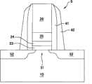
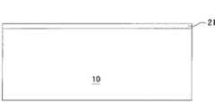
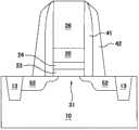
5:金属绝缘体半导体场效晶体管 10:基板5: Metal Insulator Semiconductor Field Effect Transistor 10: Substrate
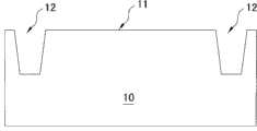
12:隔离槽 11:主动区12: Isolation slot 11: Active area
21:绝缘层 13:浅沟槽隔离21: Insulation layer 13: Shallow trench isolation
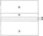
23:第一介电层/第一栅极介电层 22:暂时材料层23: First dielectric layer/first gate dielectric layer 22: Temporary material layer
25:第一栅电极层/第一栅极电极层 24:第二介电层/第二栅极介电层25: First gate electrode layer/first gate electrode layer 24: Second dielectric layer/second gate dielectric layer
27:栅电极 26:第二栅电极层/第二栅极电极层27: Gate electrode 26: Second gate electrode layer/second gate electrode layer
41:漏极延伸间隙壁 31:通道41: Drain extension spacer 31: Channel
52:源极/漏极 42:源极/漏极间隙壁52: Source/Drain 42: Source/Drain Spacers
101:第一曲线 102:第二曲线101: The first curve 102: The second curve
具体实施方式Detailed ways
较佳实施例的应用与实施将在以下详细揭露。然而,可以理解的是,本发明提供许多可供应用的创新概念,这些创新概念可在各种特定背景中加以体现。所讨论的特定实施例仅用以举例说明制造与应用本发明的特定方式,并不用以限制本发明的范围。The application and implementation of the preferred embodiments will be disclosed in detail below. It should be appreciated, however, that the present invention provides many applicable innovative concepts that can be embodied in a wide variety of specific contexts. The specific embodiments discussed are merely illustrative of specific ways to make and use the invention, and do not limit the scope of the invention.
将在一特定的范围内以不同的实施例来描述本发明,也就是锗通道场效晶体管(germanium channel field effect transistor)。然而,本发明亦可应用不同型态的装置及信道材料。The invention will be described in terms of different embodiments within a certain scope, namely germanium channel field effect transistors. However, different types of devices and channel materials are also applicable to the present invention.
形成锗、III-V族(例如砷化镓、磷化铟)以及II-VI族(例如硫化镁、氧化镁)的晶体管所面临的困难之一,就是形成具有高介电常数的栅极介电质,而不会导入缺陷,例如界面状态(interface states)或块状的电荷陷阱(charge traps)。然而,不同于硅,锗、III-V族以及II-VI族不会形成具有低缺陷密度的稳定氧化物。当然,二氧化锗具有一高缺陷密度(high defect density),例如界面的陷阱密度(interface trap densities)高于约1x10¹²/cm2。一个降低缺陷的方法就是通过将氧化物退火。然而,锗与III-V族以及II-VI族的氧化物在高温下是不稳定的。例如,二氧化锗在高于700℃时是容易爆炸(volatile)的。而且,假如暴露于湿气中,二氧化锗会分解。即使在较低的温度下(例如约400℃),锗的次氧化物(sub-oxides)仍旧不稳定。One of the difficulties in forming germanium, III-V (e.g., gallium arsenide, indium phosphide), and II-VI (e.g., magnesium sulfide, magnesium oxide) transistors is forming gate dielectrics with high dielectric constants. electrons without introducing defects such as interface states or bulk charge traps. However, unlike silicon, germanium, III-V and II-VI groups do not form stable oxides with low defect densities. Of course, germanium dioxide has a high defect density, for example, the interface trap densities are higher than about 1×10¹² /cm2 . One way to reduce defects is by annealing the oxide. However, germanium and III-V and II-VI oxides are unstable at high temperatures. For example, germanium dioxide is volatile above 700°C. Also, germanium dioxide decomposes if exposed to moisture. Even at lower temperatures (eg, about 400° C.), germanium sub-oxides are still unstable.
已经尝试过不同的研究以克服直接在锗的表面上形成高k介电层的困难。然而,在高k介电层与锗间的界面是相当有缺陷的。高界面电荷遮蔽了半导体基板的栅电位(gate potential),导致了电容的表现不佳。这是由于高k介电质成长自半导体基板10的末端锗原子。在半导体(锗)基板与高k介电层间的晶状结构的大改变,导致了由于未终结的锗或高k介电原子(或氢作为终结的原子容易因为电位而被打断)产生的大量界面陷阱(interface traps)。Various studies have been attempted to overcome the difficulty of forming a high-k dielectric layer directly on the surface of germanium. However, the interface between the high-k dielectric layer and germanium is quite defective. High interfacial charge shadows the gate potential of the semiconductor substrate, resulting in poor performance of the capacitor. This is due to the high-k dielectric grown from the terminal germanium atoms of the
再一技术是有关于在锗层上形成一硅覆盖层(silicon cap layer)或一钝化(passivation)层。硅覆盖层部分被转化成氧化硅层,以形成栅极绝缘体(gateinsulator)。可在一氧化硅层上形成一质量良好的高k介电层。当此制程的缺陷密度(defect density)是低的时候,锗的能带间隙(band gap)会低于硅。因此,锗在具有一既定的位能与掺杂(doping)下,会早于硅覆盖层前转化。因此,晶体管的通道会形成于锗层中,其位于残留的硅覆盖层下。形成于二氧化硅栅极介电质与锗通道之间的硅层,会导致晶体管电性氧化物的厚度增加。此电性氧化物的厚度增加抵销了在信道区域中增加的迁移率。Yet another technique involves forming a silicon cap layer or a passivation layer on the germanium layer. The silicon capping layer is partially converted to a silicon oxide layer to form a gate insulator. A good quality high-k dielectric layer can be formed on the silicon monoxide layer. When the defect density of the process is low, germanium has a lower band gap than silicon. Therefore, germanium, with a given potential and doping, is converted earlier than the silicon capping layer. Thus, the channel of the transistor is formed in the germanium layer, which is located under the remaining silicon capping layer. The silicon layer formed between the silicon dioxide gate dielectric and the germanium channel increases the thickness of the transistor's electrical oxide. The increased thickness of the electrical oxide counteracts the increased mobility in the channel region.
在不同的实施例中,本发明克服了形成一稳定半导体氧化物的限制。半导体氧化物的使用确保了低缺陷浓度,尽管稳定剂(stabilizer)避免了半导体氧化物的环境降解。在不同的实施例中,通过一稳定金属,半导体的氧化物因此而稳定。稳定金属与不稳定的半导体氧化物结合,并形成一稳定的氧化物,其具有低缺陷密度(例如低于约1012/cm2)。In various embodiments, the present invention overcomes the limitations of forming a stable semiconductor oxide. The use of semiconducting oxides ensures low defect concentrations, although stabilizers avoid environmental degradation of the semiconducting oxides. In various embodiments, the oxide of the semiconductor is thus stabilized by a stabilizing metal. The stable metal combines with the unstable semiconductor oxide and forms a stable oxide with a low defect density (eg, less than about 1012 /cm2 ).
在下列所举实施例中,所使用的半导体材料是主要以锗来实施,当然,在其它实施例中,所使用的半导体材料可根据实际应用情况选用III-V族化合物(例如砷化镓、磷化铟)或II-VI族化合物(例如硫化镁、氧化镁)。因此,在下列实施例中,提及锗基板及氧化锗的部分亦应可以III-V族与II-VI族基板以及III-V族与II-VI族的氧化物来取代之。In the following examples, the semiconductor material used is mainly implemented with germanium. Of course, in other embodiments, the semiconductor material used can be selected from III-V group compounds (such as gallium arsenide, gallium arsenide, indium phosphide) or II-VI compounds (e.g. magnesium sulfide, magnesium oxide). Therefore, in the following embodiments, the parts referring to the germanium substrate and germanium oxide should also be replaced by III-V and II-VI substrates and III-V and II-VI oxides.
图1是绘示金属绝缘体半导体场效晶体管(MISFET)5掺杂在半导体基板10中。在不同实施例中,半导体基板10可为一块状单晶锗基板(bulkmono-crystalline germanium substrate)、一半导体主体上覆锗层(germanium layeron a semiconductor body),例如一硅基板上覆锗层(germanium layer on a siliconsubstrate)或一绝缘体上覆锗基板(germanium-on-insulator substrate)。FIG. 1 shows a metal insulator semiconductor field effect transistor (MISFET) 5 doped in a
此金属绝缘体半导体场效晶体管5包含一栅极介电质堆叠(gate dielectricstack),其包含第一介电层23与第二介电层24。在不同实施例中,第一介电层23包含MGeO,例如一含氧化锗的氧化物(GeO)以及一稳定金属(M)氧化物。第一介电层23的组成份包含了MzGeyOx,其中x与y的比例为约0.2至约5之间,且x与z的比例为约0.2至约5之间。稳定金属(M)可为铝、铪、钛、钽、镧、锆、钨、钆、或其结合物及其相似金属。在不同实施例中,稳定金属可与氧原子产生键结,并且稳定氧化物的网络。不像独立形成在半导体基板10上的高k介电层,稳定金属并不会特别改变锗和氧化锗(Ge/GeO)间的界面,导致低界面缺陷密度,例如低于约1x1011/cm2。在不同实施例中,第一介电层23的介电常数大于氧化锗的介电常数。在某些实施例中,第一介电层23还包含卤素原子。在一实施例中,第一介电层23包含氟,例如MzGeyOxFw,其中x与y的比例为约0.2至约5之间,x与z的比例为约0.2至约5之间,以及w与y的比例为约0.01至约1之间。The
第二介电层24包含一适当的介电层以及一高k介电材料。在不同实施例中,第二介电层24的介电常数是高于第一介电层23的介电常数。在不同实施例中,使用于第二介电层24的高k介电材料具有约为或大于5的介电常数。适当的介电材料包括金属氧化物(MOx),例如二氧化铪(HfO2)、三氧化二铝(Al2O3)、二氧化锆(ZrO2)、五氧化二钽(Ta2O5)、三氧化二镧(La2O3)、氧化钆(GdOx)、氧化铝钆(GdAlOx),金属硅酸盐类(MSiyOx),例如铪硅酸盐(HfSiOx)、锆硅酸盐(ZrSiOx)、铝硅酸盐(SiAlOx),金属锗酸盐类(MGeyOx),例如铪锗酸盐(HfGeOx)、锆锗酸盐(ZrGeOx)、镧锗酸盐(LaGeOx)、钆锗酸盐(GdGeOx)或铝锗酸盐(GeAlOx)。不同实施例当然也可包括具有多种金属的高k介电材料,例如一第一金属M1与一第二金属M2。在一实施例中,可使用包含一第一金属M1与一第二金属M2的一金属氧化物来作为第二介电层24,该金属氧化物包括氧化铪铝(HfAlOx)、氧化铪锆(HfZrOx)、氧化锆铝(ZrAlOx)、氧化镧铝(LaAlOx)、氧化钽(TaAlOx)或氧化钆铝(GdAlOx)。在一些实施例中,当没有特别图示时,也可以使用上述的氮化物以及混合物。或者,第二介电层24可包含其它高k绝缘材料或其它介电材料。第二介电层24可包含由一种材料所组成的单一层或选择性的多层。The
第一栅电极层25是设置于第二介电层24上。第一栅电极层24包含一导电性材料,例如一金属栅电极材料。在不同实施例中,第一栅电极层25包含一金属氮化物,例如氮化钛(TiN)、氮化钽(TaN)、氮化钼(MoN)、氮化铪(HfN)或氮化钛铝(TiAlN)。在其它实施例中,第一栅电极层25包含碳化钛(TiC)、氮化铪(HfN)、碳化钽(TaC)、钨(W)、铝(Al)、铷(Ru)、铷钽(RuTa)、氮化钽硅(TaSiN)、镍硅化物(NiSix)、铱(Ir)、钇(Y)、镱硅化物(YbSix)、铒硅化物(ErSix)、铂(Pt)、钛(Ti)、铂钛(PtTi)、钯(Pd)、铼(Re)、铑(Rh)、硼化物、或钛(Ti)、铪(Hf)、锆(Zr)、钼(Mo)、氮化锆硅(ZrSiN)、氮化锆(ZrN)、氮化铪硅(HfSiN)、氮化钨(WN)、镍(Ni)、镨(Pr)、氮化钒(VN)、钛钨(TiW)的锑化物、或其结合物。在一实施例中,第一栅电极层25包含一掺杂多晶硅层或一硅化物层(例如硅化钛、硅化镍、硅化钽、硅化钴、硅化铂)。第一栅电极层25的厚度可根据功函数而调整。The first
第二栅电极层26是设置于第一栅电极层25上。在一实施例中,第二栅电极层26包含一掺杂多晶硅层。在不同实施例中,第二栅电极层26包含一适当的导电材料。在一实施例中,第一栅电极层25与第二栅电极层26包含相同材料。The second
金属绝缘体半导体场效晶体管5还包含一通道31,设置于邻接的源极/漏极52之间。在不同实施例中,通道31包含锗。在一实施例中,源极/漏极52包含锗。当以一相同的材料形成源极/漏极52与通道31时,有利于降低制程成本,含锗的晶体管会承受过度的漏电流(excessive leakage current)(低能量能带间隙)以及高接面电容(junction capacitance)(锗的高介电常数)。因此,在一些实施例中,源极/漏极52可包含其它材料以降低,例如,由于锗较小的能带间隙,产生的次临界泄漏(sub-threshold leakage)(源极对漏极穿隧(source to draintunneling))电流。在一实施例中,源极/漏极52包含硅。含硅的源极/漏极52将会导入一张力应变(tensile strain)至晶体管的通道31内,其可能通过通道31改善n型场效晶体管(FET)(例如具有锗(100)表面的半导体基板)。在一些实施例中,可导入一额外的材料层至通道31与源极/漏极52的接面,以降低短通道效应(short channel effort)。The Metal Insulator Semiconductor
在一实施例中,金属绝缘体半导体场效晶体管5包含漏极延伸间隙壁(drain extension spacer)41与源极/漏极间隙壁(source/drain spacer)42。在不同实施例中,间隙壁可以任何适合的形态形成,以将金属绝缘体半导体场效晶体管5不同的区域与栅电极层的任一层分离。In one embodiment, the
在一实施例中,金属绝缘体半导体场效晶体管5包含p信道晶体管或者n信道晶体管装置,然而相对于硅装置,p型晶体管(pMOS)具有可改善性能的实质电位(potential)。不像III-V族的半导体基板,单锗基板可使用于n型或p型晶体管,虽然对于较简单的积体(integration)会依序牺牲掉n型晶体管的某些性能。然而,本发明的实施例亦包含仅在p型晶体管使用一锗基板以及一以金属稳定的氧化锗(metal stabilized germanium oxide)。在不同实施例中,在说明平面晶体管时,金属绝缘体半导体场效晶体管5包含三栅极(triple gate)或双栅极(double gate)装置。In one embodiment,
图2a至2d绘示一金属绝缘体装置在不同阶段的组装。Figures 2a to 2d illustrate different stages of assembly of a metal insulator device.
请先参照图2a,提供一半导体基板10。在一实施例中,半导体基板10是一锗晶片。在不同实施例中,半导体基板10是一块状单晶硅基板(bulkmono-crystalline germanium substrate)(或是长在基板上面不然就是里面的一层)、一半导体本体上覆锗层、一锗(100)半导体晶片上的锗(110)层或是一层绝缘体上覆锗(GeOI)晶片。半导体基板10掺杂有一适当的p型或n型掺杂物,以形成一具有适当导电性的表面层,例如通过植入或退火步骤。Referring to FIG. 2a first, a
一绝缘层21是沉积在半导体基板10所暴露的部分上。在一实施例中,绝缘层21包含一氧化锗(例如氧化锗或二氧化锗)、氮化物(例如氮化锗)或者氧化物与氮化物的组成物(例如氮氧化锗或一氧化物-氮化物-氧化物的次序)。通过氧化半导体基板10来沉积绝缘层21。在一实施例中,将半导体基板10放置在一氧等离子环境下,其包含氧气/氮气、氧气、臭氧以及/或原子态的氧气,以形成一氧化层。在一实施例中,氧气的提供是将一分子状态的氧气,以流率约250sccm至约1000sccm以及约10托(torr)至约100托的氧气分压注入至等离子室内。在一实施例中,含氧的氧化制程于氧分压介于约10托至约720托下进行,氧化温度介于约250℃至约500℃。在另一实施例中,含臭氧的氧化制程于臭氧分压介于约0.005托至约0.5托下进行,氧化温度介于约200℃至约500℃。使用臭氧的氧化速度快于使用氧气的氧化速度,因此使用臭氧的分压小于使用氧气的分压。An insulating
或者,在其它实施例中,绝缘层21是以高温热氧化制程所形成。在其它实施例中,可使用任何适当的沉积技术,包含原子层沉积、等离子气相沉积或化学气相沉积。在不同实施例中,绝缘层21包含一厚度至约30埃的单一层(single mono-layer)(约2埃),在一实施例中其厚度低于16埃。Alternatively, in other embodiments, the insulating
或者,在一些实施例中,使一卤素原子,例如氟,吸附至绝缘层21中。在一实施例中,绝缘层21的形成包含形成添加氟的锗氧化物(GeOxFw)。在一实施例中,在基板10的氧化过程中,将稀释的三氟化氮(NF3)导入氧化室中。控制绝缘层21所吸附的氟总量,例如控制三氟化氮(NF3)气体的流率比例(三氟化氮(NF3)的流率/氧源的流率)。在不同实施例中,三氟化氮(NF3)的流率比例约为1x10-3至约1x10-1。或者,在一些实施例中,三氟化氮(NF3)源可在成长出少数的单层绝缘层21后关闭,如此使得卤素原子吸附于绝缘层21与基板10间的接面。卤素原子帮助修复基板10的悬吊键,且因此移除绝缘层21与基板10界面的阻陷状态(trap state)。Alternatively, in some embodiments, a halogen atom, such as fluorine, is adsorbed into the insulating
如图2b所示,在第一绝缘层21上沉积一暂时材料层22。在不同实施例中,暂时材料层22包含一稳定金属。稳定金属(M)包含铝、铪、钛、钽、镧、锆以及/或钨及其相似金属。在一实施例中,稳定金属包含铝。在一替代实施例中,暂时材料层22包含一含有稳定金属的导电层。As shown in FIG. 2 b , a
暂时材料层22的沉积可通过,例如化学气相沉积(CVD)、原子层沉积(ALD)、金属有机化学气相沉积(MOCVD)、物理气相沉积(PVD)或喷射气相沉积(JVD)来完成。暂时材料层22的厚度包含自一单一层厚度(约2埃)至约30埃,以及在一实施例中,在一实施例中其厚度低于16埃。在一实施例中,暂时材料层22的厚度是与绝缘层21大约相同。Deposition of the
在一些实施例中,可使用卤素原子的植入来使卤素原子吸附至绝缘层21与基板10的界面之间。在不同实施例中,可将氟植入至基板10、绝缘层21以及/或暂时材料层22中。In some embodiments, the implantation of halogen atoms may be used to adsorb the halogen atoms between the interface of the insulating
参照图2c,加热半导体基板10以形成一第一介电层23。在一实施例中,在一炉中加热半导体基板10约250℃至约500℃。在退火过程中,半导体(锗)基板10的原子由绝缘层21向外扩散到暂时材料层22,同时稳定金属原子由暂时材料层22向内扩散至绝缘层21。因此形成第一介电层23,其包含绝缘层21与暂时材料层22的原子而形成一介电材料。第一介电层23的组成份包含MzGeyOx,其中x与y的比例介于约0.2至约5,且其中x与z的比例介于约0.2至约5。第一介电层23的介电常数大于5。在一实施例中,第一介电层23的介电常数是大于绝缘层21的介电常数。假如卤素原子,例如氟,被吸附到基板10以及/或暂时材料层22、第一介电层23之中,可通过加热以包含氟。举例来说,假如绝缘层21包含添加氟的氧化锗(GeOxFw),随后所形成的第一介电层23包含添加氟的金属锗酸盐(MzGeyOxFw)。Referring to FIG. 2c, the
或者,在一实施例中,之后可使用原子层沉积制程形成一层薄膜,其包含有多层绝缘层21以及暂时材料层22。在一开始沉积绝缘层21之后,将气体化学性质改变成沉积一层暂时材料层22,如此可形成该层薄膜的第一次堆叠。在沉积暂时材料层22后,在第一次堆叠上形成第二次堆叠,第二次堆叠包含另一绝缘层21以及另一暂时材料层22。之后进行堆叠直到沉积至所需的厚度。在形成每一次的堆叠后,可进行一选择性的退火以形成一层第一介电层23。或者,可进行一最终退火以形成第一介电层23。Alternatively, in one embodiment, an atomic layer deposition process may be used to form a thin film, which includes multiple insulating
参照图2d,在第一介电层23上形成第二介电层24。第二介电层24包含一高k介电材料,其具有大于约0.5的介电常数。具有介电常数大于约10的适当介电材料包含有例如氧化铪(HfO2)、氧化锆(ZrO2)、氧化钽(Ta2O5)、氧化镧(La2O3)、氧化钛(TiO2)、氧化镝(Dy2O3)、氧化钇(Y2O3)、其氮化物(即前述材料其中之一的氮化物,如氧化锆的氮化物等)、或其组合(即前述材料的组合,如氧化钽与氧化镧的组合等)。或者,具有介电常数大于约5的适当介电材料包含有氧化铪硅(HfSiOx)、氧化铝(Al2O3)、氧化锆硅(ZrSiOx)、其氮化物(即前述材料其中之一的氮化物,如氧化铝的氮化物等)、氧化铪铝(HfAlOx)、氮氧化铪铝(HfAlOxN1-x-y)、氧化锆铝(ZrAlOx)、氮氧化锆铝(ZrAlOxNy)、氧化硅铝(SiAlOx)、氮氧化硅铝(SiAlOxN1-x-y)、氧化铪硅铝(HfSiAlOx)、氮氧化铪硅铝(HfSiAlOxNy)、氧化锆硅铝(ZrSiAlOx)、氮氧化锆硅铝(ZrSiAlOxNy)、或其组合(即前述材料的组合,如氧化硅铝与氧化铪硅铝的组合等)。Referring to FIG. 2d , a
第二介电层24的沉积可使用任何适当的沉积技术,包含原子层沉积、金属有机化学气相沉积以及其它气相沉积技术。在一实施例中,第二介电层24的较佳厚度介于约5埃至约100埃,当然在其它实施例中,第二介电层24也可为其它尺寸。在一些实施例中,也可略过第二介电层24而进行之后的制程。The
在第二介电层24上沉积一第一栅电极层25,其包含一导电材料(第2d图)。在不同实施例中,第一栅电极层25包含有一金属氮化物,例如氮化钛(TiN)、氮化钽(TaN)、氮化钼(MoN)、氮化铪(HfN)或氮化钛铝(TiAlN)。在一实施例中,第一栅电极层25包含一锗化物(germanide)层(例如锗化钛、锗化镍、锗化钽、锗化钴或锗化铂)。在其它实施例中,也可沉积其它适当的金属。使用化学气相沉积、物理气相沉积、原子层沉积或其它沉积技术,以沉积具有厚度介于约5埃至200埃的第一栅电极层25。On the
在第一栅电极层25上沉积一第二栅电极层26。在一实施例中,第二栅电极层26包含一掺杂多晶硅层。在不同实施例中,第二栅电极层26包含一适当的导电材料。在一实施例中,第一栅电极层25与第二栅电极层26包含一相同材料。使用化学气相沉积、物理气相沉积、原子层沉积或其它沉积技术,以沉积具有厚度介于约200埃至1000埃的第二栅电极层26。A second
之后的制程继续形成接触(contacts)以及其它任何的装置区域,以形成一金属绝缘半导体(MIS)电容。如此形成的金属绝缘半导体电容包含一第一电极,第一电极包含第一栅电极层25并与第二电极分离,第二电极包含半导体基板10。金属绝缘半导体电容的绝缘体包含第一介电层23以及第二介电层24。Subsequent processing continues with the formation of contacts and any other device regions to form a metal insulator semiconductor (MIS) capacitor. The MIS capacitor thus formed includes a first electrode, the first electrode includes the first
图3a及图3b,绘示依据本发明的实施例来组装电容。其中,图3a是一X射线光电子光谱图,而图3b绘示一电容-电压(CV)曲线。3a and 3b illustrate assembling capacitors according to an embodiment of the present invention. Wherein, FIG. 3a is an X-ray photoelectron spectrum diagram, and FIG. 3b shows a capacitance-voltage (CV) curve.
图3a绘示根据图2a至2d栅电极层在不同组装阶段的锗的X射线光电子光谱图。X射线光电子光谱是一种表面化学分析技术,用来分析在组装后栅电极层的表面化学。X射线光电子光谱图绘示所侦测到的电子强度(Y轴)对应于所侦测到的电子结合能量(X轴)。例如,对每个元素来说,特征峰值对应于原子内电子的电子组态,例如1s、2s、2p、3s等等。因此,峰值分布的改变表示键结的改变。FIG. 3 a shows X-ray photoelectron spectra of germanium at different assembly stages according to the gate electrode layer of FIGS. 2 a to 2 d. X-ray photoelectron spectroscopy is a surface chemical analysis technique used to analyze the surface chemistry of the gate electrode layer after assembly. X-ray photoelectron spectroscopy graph plotting detected electron intensity (Y-axis) versus detected electron binding energy (X-axis). For example, for each element, the characteristic peak corresponds to the electron configuration of the electrons in the atom, such as 1s, 2s, 2p, 3s, and so on. Therefore, a change in peak distribution indicates a change in bonding.
图3a绘示一第一曲线101及一第二曲线102。第一曲线101是在形成氧化锗层后的X射线光电子光谱(例如图2a的绝缘层21)。第一曲线101包含锗的一第一峰值(大约29电子能量(eV))以及来自二氧化锗(GeO2)的四价锗(Ge4+)的第二个较小的峰值(大约32.4eV)。FIG. 3 a shows a
第二曲线102是在形成第一介电材料23(如图2c所示)后的X射线光电子光谱图。由于第一介电层23的形成,峰值已变成约31.7eV(如能量差ΔE)。二氧化锗(GeO2)结合能量(在约32.4eV)在密度上实质的减少代表了二氧化锗(GeO2)键结数目的减少。The
图3b绘示为锗金属氧化半导体电容(例如以图2a至2d的方法所组装或图1所示的结构)的电容-电压曲线。这里电容是用以测量栅电极的电位。与氧化锗以及纯高k介电电容不同,锗金属氧化半导体电容的电容-电压曲线在高频率(1MHz)与低频率(100Hz)的曲线都表现出优异的性能,且没有表现出任何阻塞(pinning)。FIG. 3b shows the capacitance-voltage curve of a GeMOS capacitor (eg assembled by the method of FIGS. 2a to 2d or the structure shown in FIG. 1 ). Here the capacitance is used to measure the potential of the gate electrode. Unlike germanium oxide and pure high-k dielectric capacitors, the capacitance-voltage curve of germanium metal oxide semiconductor capacitors shows excellent performance at both high frequency (1MHz) and low frequency (100Hz) curves, and does not show any blocking ( pinning).
图4a至4g,其绘示一金属绝缘体半导体场效晶体管装置组装的不同阶段。4a to 4g, which illustrate different stages of assembly of an MISFET device.
参照图4a,在半导体基板10上形成隔离槽12。可使用已知技术来形成隔离槽12。例如,可在半导体基板10上形成一硬屏蔽层(未绘示)(如氮化硅),再图案化以暴露出隔离区域。接着,可在半导体基板10暴露出的部分蚀刻出一适当深度,通常介于约200纳米(nm)至约400纳米。隔离槽12定义出主动区11,可提供集成电路组件形成于上。Referring to FIG. 4 a , an
请参照图4b,在隔离槽12内填入一隔离材料以形成浅沟槽隔离13。举例来说,可热氧化所暴露出的硅表面以形成一薄氧化层。此外,隔离槽12可衬有一第一材料,例如一氮化物层(例如四氮化三硅(Si3N4))。此外,隔离槽12可填入一第二材料,例如一氧化物。举例来说,可进行一高密度等离子(HDP),而所形成的材料称为高密度等离子氧化物。在其它实施例中,也可使用其它沟槽填充制程,例如,通常当沟槽已经有衬时,可避免以其它填充材料进行此一步骤。Referring to FIG. 4 b , an isolation material is filled into the
如图4c(且如图2a与2b所述)所形成的一栅极绝缘堆叠包含一绝缘层21以及一暂时料层22。在不同实施例中,绝缘层21包含氧化锗(例如二氧化锗(GeO2)),且暂时材料层22包含一稳定金属。如前所述,稳定金属有助于稳定绝缘层21中的氧化物。A gate insulating stack formed in FIG. 4c (and as described in FIGS. 2a and 2b ) includes an insulating
参照图4d,一栅极介电质包含形成一第一栅极介电层23以及一第二栅极介电层24。使栅极绝缘堆叠退火以形成一第一栅极介电层23(同图2c所述)。因此第一介电层23的形成包含了绝缘层21与暂时材料层22的原子,以形成一介电材料(亦如图2c所述)。在一实施例中,第一介电层23的组成份包含了MzGeyOx,其中M是稳定金属,用以稳定氧化锗的网络。Referring to FIG. 4d , a gate dielectric includes forming a first
在第一栅极介电层23上沉积第二栅极介电层24。第二栅极介电层24包含一适当的高k介电材料,且沉积方法可通过例如化学气相沉积、原子层沉积、金属有机化学气相沉积、物理气相沉积或喷射气相沉积来完成。在一实施例中,第二栅极介电层24包含一自约5埃至约60埃的厚度。A second
在此示范实施例中,可使用相同的介电层以形成p信道或n信道晶体管的闸介电质。然而,这特征并非必须。在替代实施例中,每一p信道晶体管与n信道晶体管都可具有不同的闸介电质。例如,在一实施例中,第二栅极介电层24可选择不同的p信道晶体管与n信道晶体管。这最佳化了两装置的独立性。In this exemplary embodiment, the same dielectric layer can be used to form the gate dielectric for p-channel or n-channel transistors. However, this feature is not required. In alternative embodiments, each p-channel transistor and n-channel transistor may have a different gate dielectric. For example, in one embodiment, different p-channel transistors and n-channel transistors can be selected for the second
如图4e所示,在栅极介电质上形成栅电极27并图案化。栅电极包含如前述实施例所述的第一栅极电极层25以及第二栅极电极层26。第一栅极电极层25实质定义出栅电极的功函数。第二栅极电极层26可包含多种堆叠栅极材料,例如金属底层具有多晶硅覆盖层设置在此金属底层上。As shown in Figure 4e, a
p信道与n信道的晶体管包含第一栅极电极层25,其是由相同层所形成。在其它实施例中,不同型态的晶体管可包含不同材料以及/或不同厚度的第一栅极电极层25。The p-channel and n-channel transistors comprise a first
图案化第一栅极电极层25与第二栅极电极层26(与选择性的第一栅极介电层23以及第二栅极介电层24),并且使用已知的光刻(photolithograph)制程进行蚀刻以创造出适当图案的栅电极27。Pattern the first
如图4f所示,形成一薄层的漏极延伸间隙壁41以及源极/漏极延伸区51。漏极延伸间隙壁41是由一绝缘材料所形成,例如氧化物及/或氮化物,并且形成在栅电极27的侧壁上。通常漏极延伸间隙壁41是通过沉积一共形层(conformal layer),接着进行一非等向性蚀刻所形成的。对于多层可依照需求重复前述制程。As shown in FIG. 4f, a thin layer of
使用栅电极27作为屏蔽将源极/漏极延伸区51植入。也可依照需求进行其它植入方法(例如口袋布植(pocket implants)、环状布植(halo implants)或双扩散区(double diffused regions))。此延伸布植也定义出晶体管的通道31。The source/
假如要形成p型晶体管,使用一p型离子布植沿着n型环状布植以形成源极/漏极延伸区51。假如要形成n型晶体管,使用一n型离子布植沿着p型环状布植以形成源极/漏极延伸区51。If a p-type transistor is to be formed, a p-type ion implant is used to form the source/
参照图4g,形成源极/漏极间隙壁42以及源极/漏极区52。源极/漏极间隙壁42是形成于漏极延伸间隙壁41的侧壁上。源极/漏极区52是通过离子布植与退火所形成的。在一些实施例中,在半导体基板10形成一凹槽后,可磊晶成长源极/漏极区52。在这样实施例中,源极/漏极区52可包含一材料,以应变通道及/或最小化源极到漏极的泄漏路径。在源极/漏极区52上形成一锗化物以作为接点。在已知的半导体制程后接续之后的制程。Referring to FIG. 4g, source/
虽然本发明及其优点已详细描述如上,然应该了解到的一点是,在不偏离权利要求书所界定的本发明的精神与范围下,当可在此进行各种改变、取代以及修正。此外,本申请案的范围并非限制在说明书所描述的制程、机械、制造、物质成分、手段、方法以及步骤的特定实施例中。Although the present invention and its advantages have been described above in detail, it should be understood that various changes, substitutions and amendments can be made therein without departing from the spirit and scope of the present invention defined by the claims. Furthermore, the scope of the present application is not intended to be limited to the particular embodiments of the process, machine, manufacture, composition of matter, means, methods and steps described in the specification.
此外,本申请案的范围并非限制在说明书所描述的制程、机械、制造、物质成分、手段、方法以及步骤的特定实施例中。任何在此技术领域中具有通常知识者,将可轻易从本发明的揭露中了解到,现存或日后所发展出的可与上述的对应的实施例执行实质相同的功能、或达到实质相同的结果的制程、机械、制造、物质成分、手段、方法或步骤,可依据本发明来加以应用。因此,权利要求书用以将这类制程、机械、制造、物质成分、手段、方法或步骤涵括在其范围内。Furthermore, the scope of the present application is not intended to be limited to the particular embodiments of the process, machine, manufacture, composition of matter, means, methods and steps described in the specification. Anyone with ordinary knowledge in this technical field can easily understand from the disclosure of the present invention that the existing or future developed embodiments can perform substantially the same functions as the above-mentioned corresponding embodiments, or achieve substantially the same results The process, machinery, manufacture, material composition, means, method or steps can be applied according to the present invention. Accordingly, the appended claims are intended to include within their scope such processes, machines, manufacture, compositions of matter, means, methods, or steps.
Claims (20)
Translated fromChineseApplications Claiming Priority (4)
| Application Number | Priority Date | Filing Date | Title |
|---|---|---|---|
| US16125309P | 2009-03-18 | 2009-03-18 | |
| US61/161,253 | 2009-03-18 | ||
| US12/630,652US8124513B2 (en) | 2009-03-18 | 2009-12-03 | Germanium field effect transistors and fabrication thereof |
| US12/630,652 | 2009-12-03 |
Publications (2)
| Publication Number | Publication Date |
|---|---|
| CN101840863Atrue CN101840863A (en) | 2010-09-22 |
| CN101840863B CN101840863B (en) | 2012-03-21 |
Family
ID=42736783
Family Applications (1)
| Application Number | Title | Priority Date | Filing Date |
|---|---|---|---|
| CN201010138337.0AExpired - Fee RelatedCN101840863B (en) | 2009-03-18 | 2010-03-18 | Semiconductor device and method for manufacturing semiconductor device |
Country Status (5)
| Country | Link |
|---|---|
| US (2) | US8124513B2 (en) |
| JP (1) | JP5535706B2 (en) |
| KR (1) | KR101166437B1 (en) |
| CN (1) | CN101840863B (en) |
| TW (1) | TWI453820B (en) |
Cited By (11)
| Publication number | Priority date | Publication date | Assignee | Title |
|---|---|---|---|---|
| CN102694023A (en)* | 2011-03-25 | 2012-09-26 | 株式会社东芝 | Field-effect transistor and method of manufacturing the same |
| CN102800708A (en)* | 2011-12-28 | 2012-11-28 | 友达光电股份有限公司 | Semiconductor element and manufacturing method thereof |
| CN103367409A (en)* | 2013-07-04 | 2013-10-23 | 西安电子科技大学 | Preparation method for germanium substrate and La-based high-dielectric constant gate dielectric material |
| CN103943476A (en)* | 2014-03-31 | 2014-07-23 | 清华大学 | Semiconductor gate stacking structure and forming method thereof |
| US9401433B1 (en) | 2015-12-04 | 2016-07-26 | Industrial Technology Research Institute | P-type metal oxide semiconductor material and transistor |
| CN107533973A (en)* | 2015-04-16 | 2018-01-02 | 图尔库大学 | Fabrication of external oxides or external nitrides on semiconductors |
| US9983042B2 (en) | 2015-12-01 | 2018-05-29 | Industrial Technology Research Institute | Apparatus for detecting liquid level |
| CN109148279A (en)* | 2017-06-16 | 2019-01-04 | 恩智浦美国有限公司 | Method of processing a substrate for semiconductor device manufacture |
| CN109962112A (en)* | 2019-03-26 | 2019-07-02 | 湘潭大学 | A kind of ferroelectric gate field effect transistor and preparation method thereof |
| CN113659002A (en)* | 2020-05-12 | 2021-11-16 | 内蒙古工业大学 | With AlOXDiamond-based MISFET device of protective layer and preparation method thereof |
| CN114256345A (en)* | 2020-09-21 | 2022-03-29 | 上海华力集成电路制造有限公司 | FDSOI device structure and preparation method thereof |
Families Citing this family (16)
| Publication number | Priority date | Publication date | Assignee | Title |
|---|---|---|---|---|
| JP5403683B2 (en)* | 2010-01-22 | 2014-01-29 | 株式会社明電舎 | Oxide film formation method |
| CN102005390B (en)* | 2010-10-19 | 2012-10-17 | 复旦大学 | A kind of surface passivation method of germanium |
| JP2012231123A (en)* | 2011-04-15 | 2012-11-22 | Hitachi Kokusai Electric Inc | Semiconductor device, method of manufacturing semiconductor device, substrate processing system, and program |
| US8841701B2 (en)* | 2011-08-30 | 2014-09-23 | Taiwan Semiconductor Manufacturing Company, Ltd. | FinFET device having a channel defined in a diamond-like shape semiconductor structure |
| JP2013197121A (en)* | 2012-03-15 | 2013-09-30 | Toshiba Corp | Semiconductor device and method of manufacturing the same |
| US8580686B1 (en)* | 2012-04-23 | 2013-11-12 | Globalfoundries Inc. | Silicidation and/or germanidation on SiGe or Ge by cosputtering Ni and Ge and using an intralayer for thermal stability |
| US9059321B2 (en) | 2012-05-14 | 2015-06-16 | International Business Machines Corporation | Buried channel field-effect transistors |
| WO2014030389A1 (en)* | 2012-08-24 | 2014-02-27 | 独立行政法人科学技術振興機構 | Semiconductor structure provided with germanium-oxide-containing film on top of germanium layer, and manufacturing method therefor |
| US20140179095A1 (en)* | 2012-12-21 | 2014-06-26 | Intermolecular, Inc. | Methods and Systems for Controlling Gate Dielectric Interfaces of MOSFETs |
| US9406517B2 (en)* | 2013-03-12 | 2016-08-02 | Taiwan Semiconductor Manufacturing Co., Ltd. | SiGe surface passivation by germanium cap |
| WO2015029535A1 (en)* | 2013-08-30 | 2015-03-05 | 独立行政法人科学技術振興機構 | Semiconductor structure in which film including germanium oxide is provided on germanium layer, and method for manufacturing semiconductor structure |
| US9716176B2 (en) | 2013-11-26 | 2017-07-25 | Samsung Electronics Co., Ltd. | FinFET semiconductor devices including recessed source-drain regions on a bottom semiconductor layer and methods of fabricating the same |
| US11152214B2 (en)* | 2016-04-20 | 2021-10-19 | International Business Machines Corporation | Structures and methods for equivalent oxide thickness scaling on silicon germanium channel or III-V channel of semiconductor device |
| US10388755B1 (en) | 2018-06-04 | 2019-08-20 | International Business Machines Corporation | Stacked nanosheets with self-aligned inner spacers and metallic source/drain |
| EP3671813A1 (en) | 2018-12-21 | 2020-06-24 | IMEC vzw | Si-passivated ge gate stack |
| KR102715042B1 (en) | 2021-09-14 | 2024-10-11 | 삼성전자주식회사 | Capacitor and electronic device including the semiconductor device |
Citations (2)
| Publication number | Priority date | Publication date | Assignee | Title |
|---|---|---|---|---|
| CA2360312A1 (en)* | 2000-10-30 | 2002-04-30 | National Research Council Of Canada | Novel gate dielectric |
| CN101308788A (en)* | 2007-01-10 | 2008-11-19 | 台湾积体电路制造股份有限公司 | Semiconductor device and method for manufacturing the same |
Family Cites Families (27)
| Publication number | Priority date | Publication date | Assignee | Title |
|---|---|---|---|---|
| US5019882A (en)* | 1989-05-15 | 1991-05-28 | International Business Machines Corporation | Germanium channel silicon MOSFET |
| US5312766A (en)* | 1991-03-06 | 1994-05-17 | National Semiconductor Corporation | Method of providing lower contact resistance in MOS transistors |
| US5326721A (en)* | 1992-05-01 | 1994-07-05 | Texas Instruments Incorporated | Method of fabricating high-dielectric constant oxides on semiconductors using a GE buffer layer |
| US5521108A (en)* | 1993-09-15 | 1996-05-28 | Lsi Logic Corporation | Process for making a conductive germanium/silicon member with a roughened surface thereon suitable for use in an integrated circuit structure |
| US7145167B1 (en)* | 2000-03-11 | 2006-12-05 | International Business Machines Corporation | High speed Ge channel heterostructures for field effect devices |
| JP3736189B2 (en)* | 1999-03-30 | 2006-01-18 | セイコーエプソン株式会社 | Method for forming SiO2 film, method for manufacturing thin film transistor device, and liquid crystal display device |
| JP2000332009A (en)* | 1999-05-25 | 2000-11-30 | Sony Corp | Method of forming insulating film and manufacture of p-type semiconductor element |
| US6437392B1 (en)* | 1999-12-08 | 2002-08-20 | Agere Systems Optoelectronics Guardian Corp. | Article comprising a dielectric material of ZR-Ge-Ti-O or Hf-Ge-Ti-O and method of making the same |
| JP2001257344A (en)* | 2000-03-10 | 2001-09-21 | Toshiba Corp | Semiconductor device and method of manufacturing semiconductor device |
| US6461945B1 (en)* | 2000-06-22 | 2002-10-08 | Advanced Micro Devices, Inc. | Solid phase epitaxy process for manufacturing transistors having silicon/germanium channel regions |
| KR20030044394A (en)* | 2001-11-29 | 2003-06-09 | 주식회사 하이닉스반도체 | Method for fabricating semiconductor device with dual gate dielectric layer |
| US7271458B2 (en)* | 2002-04-15 | 2007-09-18 | The Board Of Trustees Of The Leland Stanford Junior University | High-k dielectric for thermodynamically-stable substrate-type materials |
| US6995430B2 (en)* | 2002-06-07 | 2006-02-07 | Amberwave Systems Corporation | Strained-semiconductor-on-insulator device structures |
| JP4216707B2 (en)* | 2003-12-25 | 2009-01-28 | 株式会社東芝 | Manufacturing method of semiconductor device |
| US20050224897A1 (en)* | 2004-03-26 | 2005-10-13 | Taiwan Semiconductor Manufacturing Co., Ltd. | High-K gate dielectric stack with buffer layer to improve threshold voltage characteristics |
| JP4919586B2 (en)* | 2004-06-14 | 2012-04-18 | 富士通セミコンダクター株式会社 | Semiconductor device and manufacturing method thereof |
| WO2006025350A1 (en)* | 2004-08-30 | 2006-03-09 | The University Of Tokyo | Semiconductor device and method for manufacturing the same |
| US7221006B2 (en)* | 2005-04-20 | 2007-05-22 | Freescale Semiconductor, Inc. | GeSOI transistor with low junction current and low junction capacitance and method for making the same |
| JP2006344837A (en)* | 2005-06-09 | 2006-12-21 | Matsushita Electric Ind Co Ltd | Semiconductor device and manufacturing method thereof |
| JP2007005534A (en)* | 2005-06-23 | 2007-01-11 | Toshiba Corp | Semiconductor device |
| EP1744352A3 (en)* | 2005-07-11 | 2009-08-19 | Imec | Method for forming a fully germano-silicided gate mosfet and devices obtained thereof |
| JP4589835B2 (en) | 2005-07-13 | 2010-12-01 | 富士通セミコンダクター株式会社 | Semiconductor device manufacturing method and semiconductor device |
| JP2007027505A (en)* | 2005-07-19 | 2007-02-01 | Toshiba Corp | Semiconductor device and manufacturing method thereof |
| JP4940682B2 (en)* | 2005-09-09 | 2012-05-30 | 富士通セミコンダクター株式会社 | Field effect transistor and manufacturing method thereof |
| US20070126021A1 (en)* | 2005-12-06 | 2007-06-07 | Yungryel Ryu | Metal oxide semiconductor film structures and methods |
| US8183556B2 (en)* | 2005-12-15 | 2012-05-22 | Intel Corporation | Extreme high mobility CMOS logic |
| JP2009043760A (en)* | 2007-08-06 | 2009-02-26 | Toshiba Corp | Semiconductor device |
- 2009
- 2009-12-03USUS12/630,652patent/US8124513B2/ennot_activeExpired - Fee Related
- 2010
- 2010-02-25TWTW099105465Apatent/TWI453820B/ennot_activeIP Right Cessation
- 2010-03-17KRKR1020100023676Apatent/KR101166437B1/enactiveActive
- 2010-03-18JPJP2010062807Apatent/JP5535706B2/enactiveActive
- 2010-03-18CNCN201010138337.0Apatent/CN101840863B/ennot_activeExpired - Fee Related
- 2012
- 2012-01-17USUS13/351,824patent/US8395215B2/enactiveActive
Patent Citations (2)
| Publication number | Priority date | Publication date | Assignee | Title |
|---|---|---|---|---|
| CA2360312A1 (en)* | 2000-10-30 | 2002-04-30 | National Research Council Of Canada | Novel gate dielectric |
| CN101308788A (en)* | 2007-01-10 | 2008-11-19 | 台湾积体电路制造股份有限公司 | Semiconductor device and method for manufacturing the same |
Cited By (18)
| Publication number | Priority date | Publication date | Assignee | Title |
|---|---|---|---|---|
| CN102694023A (en)* | 2011-03-25 | 2012-09-26 | 株式会社东芝 | Field-effect transistor and method of manufacturing the same |
| CN102800708A (en)* | 2011-12-28 | 2012-11-28 | 友达光电股份有限公司 | Semiconductor element and manufacturing method thereof |
| CN102800708B (en)* | 2011-12-28 | 2015-03-18 | 友达光电股份有限公司 | Semiconductor element and manufacturing method thereof |
| CN103367409B (en)* | 2013-07-04 | 2015-10-28 | 西安电子科技大学 | Based on the preparation method of the La base high-dielectric-constant gate dielectric material of germanium substrate |
| CN103367409A (en)* | 2013-07-04 | 2013-10-23 | 西安电子科技大学 | Preparation method for germanium substrate and La-based high-dielectric constant gate dielectric material |
| CN103943476B (en)* | 2014-03-31 | 2017-01-18 | 清华大学 | Semiconductor gate stacking structure and forming method thereof |
| CN103943476A (en)* | 2014-03-31 | 2014-07-23 | 清华大学 | Semiconductor gate stacking structure and forming method thereof |
| CN107533973A (en)* | 2015-04-16 | 2018-01-02 | 图尔库大学 | Fabrication of external oxides or external nitrides on semiconductors |
| US11615952B2 (en) | 2015-04-16 | 2023-03-28 | Turun Yliopisto | Manufacturing of foreign oxide or foreign nitride on semiconductor |
| US11646193B2 (en) | 2015-04-16 | 2023-05-09 | Turun Yliopisto | Manufacturing of foreign oxide or foreign nitride on semiconductor |
| US9983042B2 (en) | 2015-12-01 | 2018-05-29 | Industrial Technology Research Institute | Apparatus for detecting liquid level |
| US9401433B1 (en) | 2015-12-04 | 2016-07-26 | Industrial Technology Research Institute | P-type metal oxide semiconductor material and transistor |
| TWI566417B (en)* | 2015-12-04 | 2017-01-11 | 財團法人工業技術研究院 | P-type metal oxide semiconductor material and transistor |
| CN109148279A (en)* | 2017-06-16 | 2019-01-04 | 恩智浦美国有限公司 | Method of processing a substrate for semiconductor device manufacture |
| CN109148279B (en)* | 2017-06-16 | 2023-10-24 | 恩智浦美国有限公司 | Substrate processing method for semiconductor device fabrication |
| CN109962112A (en)* | 2019-03-26 | 2019-07-02 | 湘潭大学 | A kind of ferroelectric gate field effect transistor and preparation method thereof |
| CN113659002A (en)* | 2020-05-12 | 2021-11-16 | 内蒙古工业大学 | With AlOXDiamond-based MISFET device of protective layer and preparation method thereof |
| CN114256345A (en)* | 2020-09-21 | 2022-03-29 | 上海华力集成电路制造有限公司 | FDSOI device structure and preparation method thereof |
Also Published As
| Publication number | Publication date |
|---|---|
| JP2010219536A (en) | 2010-09-30 |
| US8395215B2 (en) | 2013-03-12 |
| US20120112282A1 (en) | 2012-05-10 |
| TW201036063A (en) | 2010-10-01 |
| CN101840863B (en) | 2012-03-21 |
| JP5535706B2 (en) | 2014-07-02 |
| KR20100105462A (en) | 2010-09-29 |
| TWI453820B (en) | 2014-09-21 |
| US20100237444A1 (en) | 2010-09-23 |
| KR101166437B1 (en) | 2012-07-19 |
| US8124513B2 (en) | 2012-02-28 |
Similar Documents
| Publication | Publication Date | Title |
|---|---|---|
| TWI453820B (en) | Semiconductor device and method thereof | |
| US7446380B2 (en) | Stabilization of flatband voltages and threshold voltages in hafnium oxide based silicon transistors for CMOS | |
| US9252229B2 (en) | Inversion thickness reduction in high-k gate stacks formed by replacement gate processes | |
| KR101282343B1 (en) | Semiconductor device with metal gate and method for manufacturing the same | |
| CN103681671B (en) | Semiconductor devices with tungsten gates electrode and its manufacturing method | |
| US7355235B2 (en) | Semiconductor device and method for high-k gate dielectrics | |
| US10847424B2 (en) | Method for forming a nanowire device | |
| US7700438B2 (en) | MOS device with nano-crystal gate structure | |
| CN1697181A (en) | Complementary metal-oxide-semiconductor structure and method of making the same | |
| EP1863097A1 (en) | Method for modulating the effective work function | |
| EP1863072A1 (en) | Method for modulating the effective work function | |
| US20140103457A1 (en) | Field effect transistor device having a hybrid metal gate stack | |
| TW202119618A (en) | Semiconductor devices and methods for forming the same | |
| TWI671806B (en) | Transistor device and method of forming the same | |
| US20080146012A1 (en) | Novel method to adjust work function by plasma assisted metal incorporated dielectric | |
| TWI528557B (en) | Method of forming a material layer in a semiconductor structure | |
| KR100843223B1 (en) | Semiconductor device adopting heterogeneous metal gate structure according to channel type and its manufacturing method | |
| US8741704B2 (en) | Metal oxide semiconductor (MOS) device with locally thickened gate oxide | |
| TW202447868A (en) | Integrated circuit structure and forming method thereof | |
| KR100712523B1 (en) | Semiconductor device having heterogeneous gate insulating film and manufacturing method thereof | |
| CN106856172A (en) | The forming method of fin formula field effect transistor | |
| JP3779556B2 (en) | Field effect transistor | |
| TWI786779B (en) | Semiconductor device with multiple threshold voltages and method for fabricating the same | |
| JP2013055274A (en) | Semiconductor device and manufacturing method therefor | |
| JP5252627B2 (en) | Semiconductor device manufacturing method and semiconductor device |
Legal Events
| Date | Code | Title | Description |
|---|---|---|---|
| C06 | Publication | ||
| PB01 | Publication | ||
| C10 | Entry into substantive examination | ||
| SE01 | Entry into force of request for substantive examination | ||
| C14 | Grant of patent or utility model | ||
| GR01 | Patent grant | ||
| CF01 | Termination of patent right due to non-payment of annual fee | Granted publication date:20120321 | |
| CF01 | Termination of patent right due to non-payment of annual fee |