CN101840659B - Electronic device - Google Patents
Electronic deviceDownload PDFInfo
- Publication number
- CN101840659B CN101840659BCN2009103009219ACN200910300921ACN101840659BCN 101840659 BCN101840659 BCN 101840659BCN 2009103009219 ACN2009103009219 ACN 2009103009219ACN 200910300921 ACN200910300921 ACN 200910300921ACN 101840659 BCN101840659 BCN 101840659B
- Authority
- CN
- China
- Prior art keywords
- light
- emitting
- electronic device
- vertical portion
- casing
- Prior art date
- Legal status (The legal status is an assumption and is not a legal conclusion. Google has not performed a legal analysis and makes no representation as to the accuracy of the status listed.)
- Expired - Fee Related
Links
Images


Classifications
- G—PHYSICS
- G09—EDUCATION; CRYPTOGRAPHY; DISPLAY; ADVERTISING; SEALS
- G09F—DISPLAYING; ADVERTISING; SIGNS; LABELS OR NAME-PLATES; SEALS
- G09F13/00—Illuminated signs; Luminous advertising
- G09F13/18—Edge-illuminated signs
- G—PHYSICS
- G02—OPTICS
- G02B—OPTICAL ELEMENTS, SYSTEMS OR APPARATUS
- G02B6/00—Light guides; Structural details of arrangements comprising light guides and other optical elements, e.g. couplings
- G02B6/0001—Light guides; Structural details of arrangements comprising light guides and other optical elements, e.g. couplings specially adapted for lighting devices or systems
- G02B6/0011—Light guides; Structural details of arrangements comprising light guides and other optical elements, e.g. couplings specially adapted for lighting devices or systems the light guides being planar or of plate-like form
- G02B6/0033—Means for improving the coupling-out of light from the light guide
- G02B6/0058—Means for improving the coupling-out of light from the light guide varying in density, size, shape or depth along the light guide
- G02B6/006—Means for improving the coupling-out of light from the light guide varying in density, size, shape or depth along the light guide to produce indicia, symbols, texts or the like
- G—PHYSICS
- G02—OPTICS
- G02B—OPTICAL ELEMENTS, SYSTEMS OR APPARATUS
- G02B6/00—Light guides; Structural details of arrangements comprising light guides and other optical elements, e.g. couplings
- G02B6/0001—Light guides; Structural details of arrangements comprising light guides and other optical elements, e.g. couplings specially adapted for lighting devices or systems
- G02B6/0011—Light guides; Structural details of arrangements comprising light guides and other optical elements, e.g. couplings specially adapted for lighting devices or systems the light guides being planar or of plate-like form
- G02B6/0013—Means for improving the coupling-in of light from the light source into the light guide
- G02B6/0015—Means for improving the coupling-in of light from the light source into the light guide provided on the surface of the light guide or in the bulk of it
- G02B6/002—Means for improving the coupling-in of light from the light source into the light guide provided on the surface of the light guide or in the bulk of it by shaping at least a portion of the light guide, e.g. with collimating, focussing or diverging surfaces
- G02B6/0021—Means for improving the coupling-in of light from the light source into the light guide provided on the surface of the light guide or in the bulk of it by shaping at least a portion of the light guide, e.g. with collimating, focussing or diverging surfaces for housing at least a part of the light source, e.g. by forming holes or recesses
Landscapes
- Physics & Mathematics (AREA)
- General Physics & Mathematics (AREA)
- Optics & Photonics (AREA)
- Engineering & Computer Science (AREA)
- Theoretical Computer Science (AREA)
- Illuminated Signs And Luminous Advertising (AREA)
Abstract
Translated fromChineseDescription
Translated fromChinese技术领域technical field
本发明涉及一种具有发光功能的电子装置。The invention relates to an electronic device with light emitting function.
背景技术Background technique
电子装置上都带有标识,用于标明厂商名称或电子装置的功能等。随着技术的进步,这些标识一般设置成可发光的,以增加对用户的吸引力。然而,现有的发光标识一般在不发光时仍旧是可见的,只是在发光时变亮,电子装置的外观在发光和不发光时变化并不大,从而减少了对用户的吸引力。All electronic devices are provided with marks, which are used to indicate the name of the manufacturer or the functions of the electronic devices. With the advancement of technology, these signs are generally set to be luminous, so as to increase the attractiveness to users. However, the existing luminous signs are generally still visible when not luminous, but become brighter when luminous, and the appearance of electronic devices does not change much when luminous and non-luminous, thereby reducing the attractiveness to users.
发明内容Contents of the invention
本发明提供一种电子装置,其带有发光时可见、不发光时不可见的标识。The invention provides an electronic device with a mark that is visible when it is luminous and invisible when it is not luminous.
所述电子装置,其包括一壳体和安装于壳体内的一发光组件。该壳体设置成半透明。该发光组件包括一发光体、一导光体和一遮光体,该导光体的顶部设置有发光标识,该遮光体套于该导光体上并开有对应于发光标识的开口,该发光体发出的光经由该导光体从该开口射出。The electronic device includes a casing and a light-emitting component installed in the casing. The casing is configured to be translucent. The light-emitting assembly includes a luminous body, a light-guiding body and a light-shielding body. A light-emitting mark is arranged on the top of the light-guiding body. The light-shielding body is set on the light-guiding body and has an opening corresponding to the light-emitting mark. The light emitted by the body is emitted from the opening through the light guide body.
由于壳体半透明,在发光体不发光时,发光标识不可见。当发光体发光时,发光标识可见。Since the casing is translucent, the luminous logo is invisible when the illuminant is not emitting light. When the illuminant emits light, the luminous logo is visible.
附图说明Description of drawings
图1是本发明一优选实施方式的电子装置的俯视图。FIG. 1 is a top view of an electronic device according to a preferred embodiment of the present invention.
图2是图1所示的电子装置的爆炸图。FIG. 2 is an exploded view of the electronic device shown in FIG. 1 .
图3是图2所示的电子装置的导光体的立体图。FIG. 3 is a perspective view of a light guide of the electronic device shown in FIG. 2 .
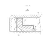
图4是图1的A-A向剖视图。Fig. 4 is a sectional view taken along line A-A of Fig. 1 .
具体实施方式Detailed ways
请参考图1,其揭示了本发明一优选实施方式的电子装置10的俯视图,该电子装置10包括一壳体11,该壳体11上可显示一发光标识12。Please refer to FIG. 1 , which shows a top view of an
参考图2,其揭示了本发明一优选实施方式的电子装置10的爆炸图,在该电子装置10的壳体11内安装有一电路基板20。在该电路基板20上除了安装有常用电子元件(图未示)外还安装有一发光组件30。Referring to FIG. 2 , it discloses an exploded view of an
在本实施方式中,壳体11的材料为塑胶。通过诸如在壳体11上涂上一层半透明漆等方式,壳体11被设置成半透明,从而,电子装置的内部结构(例如电路基板20及电路基板20上的电子元件)被遮蔽,从外界无法观察到电子装置内部的结构,而发光组件30发出的光可穿过该壳体11到达电子装置外。In this embodiment, the material of the
该发光组件30包括有一发光体40、一导光体50和一遮光体60。该发光体40和导光体50分别安装于电路基板20上。在其他结构中,该发光组件30亦可不安装在该电路基板20,而是通过数据连线与该电路基板20相连。The light-emitting
请同时参考图3、图4,导光体50大致呈L型,包括一水平部51和一垂直部52。在水平部51远离垂直部52的一端,设置有凹槽53,用以容纳该发光体40。在垂直部52的底端,设置有倾斜的反射面54。在垂直部52的顶面上,通过诸如镂空印刷等方式,设置有该发光标识12,而除了发光标识12可透光外,垂直部52的顶面的其他部分都不可透光。在本实施方式中,该发光标识12为字符“ABCD”。Please refer to FIG. 3 and FIG. 4 at the same time. The
该遮光体60套于导光体50上,在遮光体60的顶部开有对应于发光标识12的开口61,遮光体20用于使得发光体40发出的只能从开口61射出。在本实施方式中,遮光体60的材料为黑色橡胶。The light-
当发光体40不发光时,由于半透明的壳体11的遮蔽作用,从外界无法观察到该发光标识12,以及该电子装置的内部结构。当发光体40发光时,光线通过导光体50的水平部51,被反射面54反射,再通过导光体50的垂直部52,从而照亮该发光标识12。此时,从外界可看到该发光标识12(参考图1)。When the illuminant 40 is not emitting light, due to the shielding effect of the
Claims (8)
Translated fromChinesePriority Applications (2)
| Application Number | Priority Date | Filing Date | Title |
|---|---|---|---|
| CN2009103009219ACN101840659B (en) | 2009-03-17 | 2009-03-17 | Electronic device |
| US12/546,633US8240903B2 (en) | 2009-03-17 | 2009-08-24 | Electronic device with illuminated logo |
Applications Claiming Priority (1)
| Application Number | Priority Date | Filing Date | Title |
|---|---|---|---|
| CN2009103009219ACN101840659B (en) | 2009-03-17 | 2009-03-17 | Electronic device |
Publications (2)
| Publication Number | Publication Date |
|---|---|
| CN101840659A CN101840659A (en) | 2010-09-22 |
| CN101840659Btrue CN101840659B (en) | 2012-07-18 |
Family
ID=42737430
Family Applications (1)
| Application Number | Title | Priority Date | Filing Date |
|---|---|---|---|
| CN2009103009219AExpired - Fee RelatedCN101840659B (en) | 2009-03-17 | 2009-03-17 | Electronic device |
Country Status (2)
| Country | Link |
|---|---|
| US (1) | US8240903B2 (en) |
| CN (1) | CN101840659B (en) |
Families Citing this family (15)
| Publication number | Priority date | Publication date | Assignee | Title |
|---|---|---|---|---|
| US8233109B2 (en) | 2009-10-16 | 2012-07-31 | Apple Inc. | Portable computer display housing |
| US8854801B2 (en)* | 2009-10-16 | 2014-10-07 | Apple Inc. | Portable computer display housing |
| CN102914814B (en)* | 2011-08-04 | 2014-02-26 | 富泰华工业(深圳)有限公司 | Light guide column and housing assembly equipped with the light guide column |
| US9201452B2 (en)* | 2012-02-28 | 2015-12-01 | Apple Inc. | Electronic device with illuminated logo structures |
| TWM435795U (en)* | 2012-04-03 | 2012-08-11 | Inhon Internat Co Ltd | Lighting structure |
| KR20150059751A (en)* | 2012-09-20 | 2015-06-02 | 톰슨 라이센싱 | Panel illumination system |
| CN103456249A (en)* | 2013-01-17 | 2013-12-18 | 宁波海歌电器有限公司 | Icon light-emitting display system |
| KR102362530B1 (en)* | 2014-11-20 | 2022-02-15 | 엘지전자 주식회사 | Electronic device |
| MY184817A (en)* | 2014-11-24 | 2021-04-23 | Interdigital Ce Patent Holdings | Light emission structure and device with light emission structure |
| US11416082B1 (en)* | 2017-09-05 | 2022-08-16 | Apple Inc. | Input devices with glyphs having a semitransparent mirror layer |
| CN108508525A (en)* | 2018-04-19 | 2018-09-07 | Oppo广东移动通信有限公司 | Light guide structure, shell and electronic device |
| NL2024378B1 (en)* | 2019-12-04 | 2021-08-31 | Microsoft Technology Licensing Llc | Systems and methods for illuminated logo movement |
| TWM595319U (en)* | 2019-12-24 | 2020-05-11 | 大陸商東莞寶德電子有限公司 | Keyboard with light guide name plate |
| TWI758232B (en)* | 2021-10-27 | 2022-03-11 | 華碩電腦股份有限公司 | Electronic device |
| TWI832802B (en) | 2023-09-27 | 2024-02-11 | 群光電能科技股份有限公司 | Adapter with illuminated pattern |
Citations (5)
| Publication number | Priority date | Publication date | Assignee | Title |
|---|---|---|---|---|
| JP2001100680A (en)* | 1999-09-28 | 2001-04-13 | Mori Cubic Art:Kk | Structure of nameplate |
| CN2684312Y (en)* | 2003-10-16 | 2005-03-09 | 河北格林光电技术有限公司 | LED illuminated display panel |
| CN2723814Y (en)* | 2004-06-10 | 2005-09-07 | 陈荣煌 | Small night lamp structure of semiconductor light emitting element |
| CN2785080Y (en)* | 2004-08-16 | 2006-05-31 | 罗迅 | Vehicle top advertisement with illuminating body |
| CN200956230Y (en)* | 2006-09-29 | 2007-10-03 | 王雷 | LED luminous name plate |
Family Cites Families (4)
| Publication number | Priority date | Publication date | Assignee | Title |
|---|---|---|---|---|
| US6712481B2 (en)* | 1995-06-27 | 2004-03-30 | Solid State Opto Limited | Light emitting panel assemblies |
| US20040085746A1 (en)* | 2002-11-05 | 2004-05-06 | Chen Shih Ling | Instrument panel with colorful illumination |
| US20040095741A1 (en)* | 2002-11-14 | 2004-05-20 | Shao-Hsiung Chen | Side-illuminated advertisement board |
| TWI283421B (en)* | 2005-03-11 | 2007-07-01 | Coretronic Corp | Backlight button assembly |
- 2009
- 2009-03-17CNCN2009103009219Apatent/CN101840659B/ennot_activeExpired - Fee Related
- 2009-08-24USUS12/546,633patent/US8240903B2/ennot_activeExpired - Fee Related
Patent Citations (5)
| Publication number | Priority date | Publication date | Assignee | Title |
|---|---|---|---|---|
| JP2001100680A (en)* | 1999-09-28 | 2001-04-13 | Mori Cubic Art:Kk | Structure of nameplate |
| CN2684312Y (en)* | 2003-10-16 | 2005-03-09 | 河北格林光电技术有限公司 | LED illuminated display panel |
| CN2723814Y (en)* | 2004-06-10 | 2005-09-07 | 陈荣煌 | Small night lamp structure of semiconductor light emitting element |
| CN2785080Y (en)* | 2004-08-16 | 2006-05-31 | 罗迅 | Vehicle top advertisement with illuminating body |
| CN200956230Y (en)* | 2006-09-29 | 2007-10-03 | 王雷 | LED luminous name plate |
Also Published As
| Publication number | Publication date |
|---|---|
| US8240903B2 (en) | 2012-08-14 |
| CN101840659A (en) | 2010-09-22 |
| US20100238667A1 (en) | 2010-09-23 |
Similar Documents
| Publication | Publication Date | Title |
|---|---|---|
| CN101840659B (en) | Electronic device | |
| CN101620486B (en) | Electronic device and touch sensor film | |
| CN101807482B (en) | Key module and handheld electronic device with same | |
| TWI432998B (en) | Input device with illuminated roller | |
| KR100639732B1 (en) | Touch type button device and electronic device using same | |
| US20110050986A1 (en) | Window for portable electronic device | |
| CN101932986B (en) | Electronic devices with diffuse backlit displays | |
| US20110296724A1 (en) | Electronic device with pattern-displaying function | |
| US20040189604A1 (en) | Computer mouse with ornamental light source | |
| CN102097228A (en) | Key panel and manufacturing method thereof | |
| CN204256625U (en) | Printing opacity display structure part and terminal | |
| CN101727140B (en) | visual design display device | |
| CN207216642U (en) | A fingerprint module with logo light-emitting and LED indication functions | |
| TWI691249B (en) | Electronic device | |
| CN111448762B (en) | Backlight user interface | |
| TW201405612A (en) | Knob structure and electronic device thereof | |
| CN107516034A (en) | a mobile terminal | |
| CN101853618B (en) | Luminous sign display combination | |
| TW201035924A (en) | Electronic device | |
| JP2011211167A (en) | Housing, and electronic device using the same | |
| CN101655231A (en) | Combined type signal receiving device | |
| JP2011065843A (en) | Lighting system, electronic device including the same, and method of producing the lighting system | |
| CN223245053U (en) | A notebook computer shell with luminous logo | |
| CN102208297B (en) | Key panel | |
| TWI362020B (en) | Illuminated sign display assembly |
Legal Events
| Date | Code | Title | Description |
|---|---|---|---|
| C06 | Publication | ||
| PB01 | Publication | ||
| C10 | Entry into substantive examination | ||
| SE01 | Entry into force of request for substantive examination | ||
| C14 | Grant of patent or utility model | ||
| GR01 | Patent grant | ||
| CF01 | Termination of patent right due to non-payment of annual fee | Granted publication date:20120718 Termination date:20150317 | |
| EXPY | Termination of patent right or utility model |