CN101835079B - Capacitance type minitype silicon microphone and preparation method thereof - Google Patents
Capacitance type minitype silicon microphone and preparation method thereofDownload PDFInfo
- Publication number
- CN101835079B CN101835079BCN 201010142506CN201010142506ACN101835079BCN 101835079 BCN101835079 BCN 101835079BCN 201010142506CN201010142506CN 201010142506CN 201010142506 ACN201010142506 ACN 201010142506ACN 101835079 BCN101835079 BCN 101835079B
- Authority
- CN
- China
- Prior art keywords
- diaphragm
- substrate
- layer
- insulating material
- sacrificial layer
- Prior art date
- Legal status (The legal status is an assumption and is not a legal conclusion. Google has not performed a legal analysis and makes no representation as to the accuracy of the status listed.)
- Active
Links
- 229910052710siliconInorganic materials0.000titleclaimsabstractdescription26
- 239000010703siliconSubstances0.000titleclaimsabstractdescription26
- 238000002360preparation methodMethods0.000titleclaimsabstractdescription12
- XUIMIQQOPSSXEZ-UHFFFAOYSA-NSiliconChemical compound[Si]XUIMIQQOPSSXEZ-UHFFFAOYSA-N0.000titleclaimsdescription15
- 239000000758substrateSubstances0.000claimsabstractdescription70
- 239000011810insulating materialSubstances0.000claimsabstractdescription45
- 229910052751metalInorganic materials0.000claimsdescription22
- 239000002184metalSubstances0.000claimsdescription22
- 238000005530etchingMethods0.000claimsdescription21
- 238000000034methodMethods0.000claimsdescription21
- 238000002347injectionMethods0.000claimsdescription16
- 239000007924injectionSubstances0.000claimsdescription16
- 239000000463materialSubstances0.000claimsdescription15
- 238000000151depositionMethods0.000claimsdescription12
- 230000008021depositionEffects0.000claimsdescription8
- 229910021420polycrystalline siliconInorganic materials0.000claimsdescription8
- 229920005591polysiliconPolymers0.000claimsdescription8
- PXHVJJICTQNCMI-UHFFFAOYSA-NNickelChemical compound[Ni]PXHVJJICTQNCMI-UHFFFAOYSA-N0.000claimsdescription6
- 239000002131composite materialSubstances0.000claimsdescription6
- 230000000873masking effectEffects0.000claimsdescription6
- 239000004642PolyimideSubstances0.000claimsdescription4
- 229920001721polyimidePolymers0.000claimsdescription4
- BQCADISMDOOEFD-UHFFFAOYSA-NSilverChemical compound[Ag]BQCADISMDOOEFD-UHFFFAOYSA-N0.000claimsdescription3
- 229910052782aluminiumInorganic materials0.000claimsdescription3
- XAGFODPZIPBFFR-UHFFFAOYSA-NaluminiumChemical compound[Al]XAGFODPZIPBFFR-UHFFFAOYSA-N0.000claimsdescription3
- 229910052793cadmiumInorganic materials0.000claimsdescription3
- BDOSMKKIYDKNTQ-UHFFFAOYSA-Ncadmium atomChemical compound[Cd]BDOSMKKIYDKNTQ-UHFFFAOYSA-N0.000claimsdescription3
- PCHJSUWPFVWCPO-UHFFFAOYSA-NgoldChemical compound[Au]PCHJSUWPFVWCPO-UHFFFAOYSA-N0.000claimsdescription3
- 229910052737goldInorganic materials0.000claimsdescription3
- 239000010931goldSubstances0.000claimsdescription3
- 229910052759nickelInorganic materials0.000claimsdescription3
- 239000005360phosphosilicate glassSubstances0.000claimsdescription3
- 229910052709silverInorganic materials0.000claimsdescription3
- 239000004332silverSubstances0.000claimsdescription3
- 238000004519manufacturing processMethods0.000abstractdescription15
- 239000003990capacitorSubstances0.000abstractdescription7
- 238000011112process operationMethods0.000abstractdescription2
- 238000010586diagramMethods0.000description11
- 239000012528membraneSubstances0.000description11
- 239000010408filmSubstances0.000description9
- 238000000137annealingMethods0.000description5
- 229910052581Si3N4Inorganic materials0.000description4
- 238000013016dampingMethods0.000description4
- 230000035945sensitivityEffects0.000description4
- HQVNEWCFYHHQES-UHFFFAOYSA-Nsilicon nitrideChemical compoundN12[Si]34N5[Si]62N3[Si]51N64HQVNEWCFYHHQES-UHFFFAOYSA-N0.000description4
- 238000005516engineering processMethods0.000description2
- 230000003071parasitic effectEffects0.000description2
- FGUUSXIOTUKUDN-IBGZPJMESA-NC1(=CC=CC=C1)N1C2=C(NC([C@H](C1)NC=1OC(=NN=1)C1=CC=CC=C1)=O)C=CC=C2Chemical compoundC1(=CC=CC=C1)N1C2=C(NC([C@H](C1)NC=1OC(=NN=1)C1=CC=CC=C1)=O)C=CC=C2FGUUSXIOTUKUDN-IBGZPJMESA-N0.000description1
- VYPSYNLAJGMNEJ-UHFFFAOYSA-NSilicium dioxideChemical compoundO=[Si]=OVYPSYNLAJGMNEJ-UHFFFAOYSA-N0.000description1
- 230000007123defenseEffects0.000description1
- 230000007812deficiencyEffects0.000description1
- 238000005137deposition processMethods0.000description1
- 238000001514detection methodMethods0.000description1
- 230000000694effectsEffects0.000description1
- 238000001914filtrationMethods0.000description1
- 230000002093peripheral effectEffects0.000description1
- 229920001690polydopaminePolymers0.000description1
- 238000004886process controlMethods0.000description1
- 239000004065semiconductorSubstances0.000description1
- 229910052814silicon oxideInorganic materials0.000description1
- 239000000243solutionSubstances0.000description1
- 230000005236sound signalEffects0.000description1
- 239000010409thin filmSubstances0.000description1
Images


Landscapes
- Electrostatic, Electromagnetic, Magneto- Strictive, And Variable-Resistance Transducers (AREA)
Abstract
Translated fromChinese
Description
Translated fromChinese技术领域technical field
本发明涉及一种硅麦克风及其制备方法,尤其是一种电容式微型硅麦克风及其制备方法,具体地说是一种利用MEMS技术的微型硅麦克风及其制备方法。The invention relates to a silicon microphone and a preparation method thereof, in particular to a capacitive micro-silicon microphone and a preparation method thereof, in particular to a micro-silicon microphone utilizing MEMS technology and a preparation method thereof.
背景技术Background technique
MEMS(Micro-Electro-Mechanical Systems)技术是几年来高速发展的一项高新技术,与传统对应器件相比,MEMS器件在体积、功耗、重量等方面都具有十分明显的优势,而且其采用先进的半导体制造工艺,可以实现MEMS器件的批量制造,能极好的控制生产成本,提高器件的一致性。对于目前的MEMS产品,加速度计、压力传感器、陀螺仪、微镜、硅麦克风等都已经实现了批量生产,在相应的市场上都占有了一定的份额。MEMS (Micro-Electro-Mechanical Systems) technology is a high-tech that has developed rapidly in the past few years. Compared with traditional counterparts, MEMS devices have obvious advantages in terms of volume, power consumption, and weight. The advanced semiconductor manufacturing process can realize the batch manufacturing of MEMS devices, can control the production cost extremely well, and improve the consistency of the devices. For the current MEMS products, accelerometers, pressure sensors, gyroscopes, micromirrors, silicon microphones, etc. have all been mass-produced and have occupied a certain share in the corresponding market.
硅麦克风耐高温、耗电量小以及体积小等特点,使得它在移动电话、助听器、笔记本电脑、PDA、摄像机等视听产品以及国防、国家安全等相关领域应用将更加广泛。从麦克风市场的预测和发展来看,硅麦克风成为传统驻极体麦克风的替代产品已经毋庸置疑,它提供了令声学工程师相当满意的相似的甚至更好的声学性能。硅麦克风在几年以后将会成为麦克风市场上的主要产品。Silicon microphones are characterized by high temperature resistance, low power consumption, and small size, making them more widely used in audio-visual products such as mobile phones, hearing aids, notebook computers, PDAs, and cameras, as well as in related fields such as national defense and national security. From the forecast and development of the microphone market, silicon microphones have become an undoubted alternative to traditional electret microphones, providing similar or even better acoustic performance that is quite satisfactory to acoustic engineers. Silicon microphones will be a staple in the microphone market in a few years.
为了开发出高灵敏度和宽带宽的麦克风,高性能振膜的制作至关重要,振膜制作面临的一个主要问题就是振膜应力的控制。现有薄膜的制作主要采用淀积的方法得到,通过淀积得到的振膜会存在较大的残余应力,残余应力对微型硅麦克风的性能有较大影响,大的残余应力能大幅度降低麦克风的灵敏度,压应力还能减小麦克风的耐压能力,严重时能使得麦克风无法正常工作。另外,背极板的制作也至关重要,刚性背极是硅麦克风有良好频率特性和低噪声的前提条件。In order to develop a microphone with high sensitivity and wide bandwidth, the production of high-performance diaphragm is very important. One of the main problems faced by diaphragm production is the control of diaphragm stress. The production of existing thin films is mainly obtained by deposition. The diaphragm obtained by deposition will have a large residual stress. The residual stress has a great impact on the performance of the micro silicon microphone. The large residual stress can greatly reduce the microphone performance. The sensitivity of the microphone, the pressure stress can also reduce the pressure resistance of the microphone, and in severe cases, it can make the microphone unable to work normally. In addition, the production of the back plate is also very important, and the rigid back plate is a prerequisite for good frequency characteristics and low noise of the silicon microphone.
目前改善振膜残余应力通常有两种方法,一是通过附加工艺,用退火的方式,这种方式对工艺的控制要求极高,重复性不是很好;另外一种是通过结构调整,如制作自由膜结构,但这种结构的制作会导致工艺复杂度的增加,可能需要添加多步工艺,来控制振膜。而实现刚性背极也是麦克风制作过程中的一大难点,目前也是有两种主要方法来解决,一是制作厚背极,但是通过常规的淀积工艺很难得到需要的厚背极;还有一种方法是通过结构调整来提高背极板的刚性,但也是要增加工艺的复杂度。At present, there are usually two ways to improve the residual stress of the diaphragm. One is to use an additional process and annealing. This method requires extremely high process control and the repeatability is not very good; the other is through structural adjustment, such as manufacturing Free membrane structure, but the fabrication of this structure will lead to an increase in process complexity, and it may be necessary to add a multi-step process to control the diaphragm. Realizing a rigid back electrode is also a major difficulty in the microphone manufacturing process. At present, there are two main methods to solve it. One is to make a thick back electrode, but it is difficult to obtain the required thick back electrode through conventional deposition processes; One method is to improve the rigidity of the back plate through structural adjustment, but it also increases the complexity of the process.
发明内容Contents of the invention
本发明的目的是克服现有技术中存在的不足,提供一种电容式微型硅麦克风及其制备方法,其制造成本低、成品率高、工艺操作简单及满足小尺寸的要求。The purpose of the present invention is to overcome the deficiencies in the prior art and provide a capacitive micro-silicon microphone and its preparation method, which has low manufacturing cost, high yield, simple process operation and small size requirements.
按照本发明提供的技术方案,所述电容式微型硅麦克风,包括基板;所述基板的中心区淀积有振膜;基板对应于设置基板的表面还淀积有绝缘材料层;所述绝缘材料层覆盖在基板与振膜的表面,且与振膜间形成空腔;绝缘材料层与振膜相对应的内壁上设置固定连接的背极板,所述背极板与振膜形成电容结构;绝缘材料层与振膜相对应的外壁上设置若干声孔,所述声孔与绝缘材料层、振膜形成的腔体相连通;基板对应于设置振膜的下部设置声腔,所述声腔的深度从基板对应于设置振膜另一端表面延伸到振膜。According to the technical solution provided by the present invention, the capacitive micro-silicon microphone includes a substrate; a diaphragm is deposited in the central area of the substrate; an insulating material layer is also deposited on the surface of the substrate corresponding to the setting substrate; the insulating material The layer covers the surface of the substrate and the diaphragm, and forms a cavity with the diaphragm; the insulating material layer is provided with a fixedly connected back plate on the inner wall corresponding to the diaphragm, and the back plate and the diaphragm form a capacitive structure; A number of sound holes are arranged on the outer wall corresponding to the insulating material layer and the diaphragm, and the sound holes are connected with the cavity formed by the insulating material layer and the diaphragm; the base plate is corresponding to the lower part of the vibrating film. The sound cavity is set, and the depth of the sound cavity is Extend from the surface of the substrate corresponding to the other end of the diaphragm to the diaphragm.
所述振膜的一端设置振膜电极,所述振膜电极与振膜电性连接;所述背极板上设有背极板电极,所述背极板电极与背极板电性连接。所述基板对应于淀积振膜的表面设有纹膜槽。所述绝缘材料层的材料包括氮化硅及聚酰亚胺。所述振膜上设有刻蚀孔。A diaphragm electrode is provided at one end of the diaphragm, and the diaphragm electrode is electrically connected to the diaphragm; a back plate electrode is provided on the back plate, and the back plate electrode is electrically connected to the back plate. The surface of the substrate corresponding to the deposited diaphragm is provided with a film groove. The material of the insulating material layer includes silicon nitride and polyimide. The diaphragm is provided with etching holes.
所述电容式微型硅麦克风的制备方法包括如下步骤:The preparation method of described capacitive miniature silicon microphone comprises the steps:
a、提供基板,并在基板的表面上设置纹膜槽;b、在所述基板对应于设置纹膜槽的表面淀积振膜;c、选择性的掩蔽和刻蚀振膜,得到基板中心区的振膜;d、在上述基板对应于设置振膜的表面上淀积牺牲层,所述牺牲层覆盖基板及振膜相对应的表面;e、选择性的掩蔽和刻蚀牺牲层,得到基板中心区的牺牲层,并在振膜的一端形成金属注入孔,所述金属注入孔从牺牲层的表面延伸到振膜;f、在牺牲层的表面及金属注入孔内均淀积金属,在牺牲层的表面上形成背极板,所述背极板位于振膜的上方;所述振膜对应于设置金属注入孔的表面形成振膜电极;g、在基板对应于设置牺牲层的表面上淀积绝缘材料,形成绝缘材料层,所述绝缘材料层包覆基板、牺牲层、背极板及振膜电极的表面;h、选择性的掩蔽和刻蚀绝缘材料层,去除振膜电极上的绝缘材料层,在所述背极板上得到背极板电极与声孔,所述声孔从绝缘材料层的表面延伸到牺牲层;i、选择性的掩蔽和刻蚀基板对应于淀积振膜的另一表面,在基板对应于淀积振膜的另一端形成声腔,所述声腔位于振膜的下方;声腔的深度从基板对应于设置振膜的另一端表面延伸到振膜;j、刻蚀牺牲层,去除绝缘材料层包围的牺牲层。a. Provide a substrate, and set a textured groove on the surface of the substrate; b. Deposit a diaphragm on the surface of the substrate corresponding to the textured groove; c. Selectively mask and etch the diaphragm to obtain the center of the substrate The vibrating membrane in the region; d, depositing a sacrificial layer on the surface corresponding to the vibrating membrane on the above-mentioned substrate, and the sacrificial layer covers the corresponding surface of the substrate and the vibrating membrane; e, selectively masking and etching the sacrificial layer to obtain The sacrificial layer in the central area of the substrate, and form a metal injection hole at one end of the diaphragm, and the metal injection hole extends from the surface of the sacrificial layer to the diaphragm; f, metal is deposited on the surface of the sacrificial layer and in the metal injection hole, Form a back pole plate on the surface of the sacrificial layer, and the back pole plate is located above the diaphragm; the diaphragm electrode is formed on the surface corresponding to the metal injection hole; g, on the substrate corresponding to the surface of the sacrificial layer Deposit an insulating material on the top to form an insulating material layer, and the insulating material layer covers the surface of the substrate, the sacrificial layer, the back plate and the diaphragm electrode; h, selectively mask and etch the insulating material layer to remove the diaphragm electrode The insulating material layer on the upper plate, the back plate electrode and the sound hole are obtained on the back plate, and the sound hole extends from the surface of the insulating material layer to the sacrificial layer; i, selective masking and etching of the substrate correspond to the deposition On the other surface of the deposited diaphragm, an acoustic cavity is formed at the other end of the substrate corresponding to the deposited diaphragm, and the acoustic cavity is located below the diaphragm; the depth of the acoustic cavity extends from the surface of the other end of the substrate corresponding to the diaphragm to the diaphragm; j. Etching the sacrificial layer to remove the sacrificial layer surrounded by the insulating material layer.
所述步骤c中,选择性的掩蔽和刻蚀振膜,得到位于基板中心区的振膜,并在振膜上形成刻蚀孔。所述振膜为导电多晶硅或氧化支撑层、氧化层与导电层形成的复合结构。所述步骤f中淀积的金属包括金、镉、镍或银。所述牺牲层的材料包括磷硅玻璃或铝。In the step c, the diaphragm is selectively masked and etched to obtain a diaphragm located in the central area of the substrate, and an etching hole is formed on the diaphragm. The diaphragm is a composite structure formed of conductive polysilicon or an oxide support layer, an oxide layer and a conductive layer. The metal deposited in step f includes gold, cadmium, nickel or silver. The material of the sacrificial layer includes phosphosilicate glass or aluminum.
本发明的优点:振膜结构设计灵活,可为纹膜结构,也可为平膜结构。振膜可采用单一的多晶硅材料通过高温退火工艺形成,也可以采用绝缘支撑层、绝缘层与导电层相互配合形成,达到来降低残余应力的目的。通过牺牲层与绝缘材料层的设置,背极板与振膜间的距离可控,既能满足较强的刚性要求,又能减小寄生电容。制备电容式微型硅麦克风的方法成品率高,成本低,工艺容易实现,能满足小尺寸要求,并且适合大批量生产。The invention has the advantages that the vibration membrane structure is flexible in design, and can be a patterned membrane structure or a flat membrane structure. The diaphragm can be formed by a single polysilicon material through a high-temperature annealing process, or an insulating support layer, an insulating layer and a conductive layer can be formed in cooperation to achieve the purpose of reducing residual stress. Through the setting of the sacrificial layer and the insulating material layer, the distance between the back plate and the diaphragm can be controlled, which can not only meet the strong rigidity requirement, but also reduce the parasitic capacitance. The method for preparing the capacitive micro-silicon microphone has high yield, low cost, easy process realization, can meet the requirement of small size, and is suitable for mass production.
附图说明Description of drawings
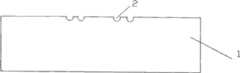
图1为本发明的结构示意图。Fig. 1 is a structural schematic diagram of the present invention.
图2~图10为本发明具体实施工艺步骤示意图,其中:Fig. 2~Fig. 10 are schematic diagrams of the specific implementation process steps of the present invention, wherein:
图2为基板上形成纹膜槽后的结构示意图。FIG. 2 is a schematic structural view of a film groove formed on a substrate.
图3为形成绝缘支撑层与绝缘层后的结构示意图。FIG. 3 is a schematic structural view after forming an insulating support layer and an insulating layer.
图4为刻蚀振膜与绝缘层后的结构示意图。FIG. 4 is a schematic diagram of the structure after etching the diaphragm and insulating layer.
图5为形成牺牲层后的结构示意图。FIG. 5 is a schematic diagram of the structure after forming the sacrificial layer.
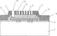
图6为形成背极板后的结构示意图。FIG. 6 is a schematic diagram of the structure after the back plate is formed.
图7为形成声孔后的结构示意图。Fig. 7 is a schematic diagram of the structure after forming the acoustic hole.
图8为形成声腔后的结构示意图。Fig. 8 is a schematic diagram of the structure after forming the acoustic cavity.
图9为去除牺牲层后的结构示意图。FIG. 9 is a schematic diagram of the structure after removing the sacrificial layer.
图10为本发明具有刻蚀孔的结构示意图。Fig. 10 is a schematic diagram of the structure of the present invention with etching holes.
图11为一种振膜的结构示意图。FIG. 11 is a schematic structural diagram of a vibrating membrane.
具体实施方式Detailed ways
下面结合具体附图和实施例对本发明作进一步说明。The present invention will be further described below in conjunction with specific drawings and embodiments.
如图1~图11所示:本发明包括基板1、纹膜槽2、绝缘支撑层3、绝缘层4、振膜5、牺牲层6、振膜电极7、背极板8、绝缘材料层9、声孔10、声腔11、可动梁12、刻蚀孔13及金属注入孔14As shown in Figures 1 to 11: the present invention includes a
如图1和图10所示:所述基板1的表面上凹设有纹膜槽2,基板1对应于设置纹膜槽2的表面淀积振膜5。所述振膜5为导电多晶硅或绝缘支撑层3、绝缘层4与导电层形成复合结构。当振膜5为绝缘支撑层3、绝缘层4与导电层形成复合结构时,绝缘支撑层3淀积在基板1对应于设置纹膜槽2的表面;所述绝缘支撑层3上再依次淀积绝缘层4与导电层;通过绝缘支撑层3与绝缘层4的相互配合,能够减少振膜5的残余应力。振膜5也可以采用多晶硅材料,但是需要对淀积的导电多晶硅进行高温退火。所述振膜5位于基板1的中心区;振膜5为绝缘支撑层3、绝缘层4与导电层形成的复合结构时,通过选择性的掩蔽和刻蚀复合结构,使绝缘支撑层3、绝缘层4与导电层形成的振膜5位于基板1的中心区。As shown in FIG. 1 and FIG. 10 : the surface of the
所述基板1上还设有绝缘材料层9;所述绝缘材料层9覆盖在基板1的表面,并与振膜5形成空腔。所述绝缘材料层9的材料为氮化硅或聚酰亚胺等其他材料。绝缘材料层9与振膜5相对应的内壁上设置背极板8,所述背极板8与振膜5具有一定的距离,分别形成电容的上极板与下极板,背极板8与振膜5构成电容结构。所述绝缘材料层9与振膜5一端相对应的表面设置金属注入孔14,所述金属注入孔14从绝缘材料层9表面伸入到振膜5的端部,从而将绝缘材料层9与振膜5形成的空腔与外部相连通。振膜5对应于设置金属注入孔14的端部淀积有振膜电极7,所述振膜电极7与振膜5电性连接。所述背极板8上设置有背极板电极,所述背极板电极与背极板8电性连接。The
背极板8的上部设置声孔10,所述声孔10为阵列设置。所述声孔10与绝缘材料层9、振膜5形成的腔体相连通。声孔10按振膜5以及背极板8形状排成阵列结构,可以用于形成过滤一定频率或一定频率范围内的声学滤波器,传播声压,调节振膜5与背极板8之间的阻尼,减小噪声;所述声孔10可为圆形、方形、椭圆等任意形状,不同形状的声孔,具有不同的性能影响,如圆形声孔,有利于释放空气压力,更有效减小压膜阻尼,但是会增加工艺制作的复杂性;方形声孔容易制作,但是会引起应力集中问题,也会影响麦克风性能。Acoustic holes 10 are arranged on the upper part of the
基板1对应于设置振膜5的下部设置有声腔11,所述声腔11位于振膜5的正下方。声腔11的深度从基板1对应于设置振膜5另一端的表面,延伸到振膜5;声腔11的宽度小于振膜5的长度。所述振膜5上设有刻蚀孔13,所述刻蚀孔13能够减小阻尼,平衡声压。腔体11的大小直接影响硅麦克风的性能,特别是其低频特性。在不影响芯片尺寸的前提下,尽量增大声腔11;声腔的形状根据不同的工艺可以为圆形或方形,由于受振膜5形状以及麦克风性能的影响,声腔11的形状也需要根据振膜5的形状来设计。The
图11为振膜5的结构示意图。如图11所示,绝缘支撑层3、绝缘层4及导电层形成振膜5。纹膜槽2设置在绝缘支撑层3、绝缘层4及导电层形成振膜5的内圈。所述振膜5上设有刻蚀孔13,所述刻蚀孔13均匀排列在振膜5上。为了提高麦克风的灵敏度,所述振膜5周面上还设置有可动梁12。FIG. 11 is a schematic structural diagram of the
上述结构的电容式微型硅麦克风结构通过如下工艺步骤实现:The capacitive miniature silicon microphone structure of the above structure is realized through the following process steps:
a、提供基板1,并在基板1的表面上设置纹膜槽2,如图2所示;a. A
当基板1上不设置纹膜槽2时,基板1上就能够得到对应的平膜的振膜5结构;所述基板1的材料为硅;When the
b、在所述基板1对应于设置纹膜槽2的表面淀积振膜5,所述基板1的表面及纹膜槽2内均形成振膜5,形成纹膜结构的振膜5;b. Deposit a
所述振膜5可以是在基板1的对应于设置纹膜槽2的表面淀积导电多晶硅并经高温退火形成;所述振膜5也可以是在基板1对应于设置纹膜槽2的表面淀积绝缘支撑层3、绝缘层4及导电层形成,如图3所示;所述绝缘支撑层3与绝缘层4间相互配合,能够减小振膜5的残余应力;所述绝缘支撑层3的材料可以为氧化硅;绝缘层4的材料可以为氮化硅;The
c、选择性的掩蔽和刻蚀振膜5,得到基板1中心区的振膜5;c. Selectively mask and etch the
当振膜5由绝缘支撑层3、绝缘层4及导电层形成时,绝缘支撑层3、绝缘层4及导电层均位于基板1的中心区,如图4所示;When the
选择性的掩蔽和刻蚀振膜5,得到位于基板1中心区的振膜5,并在振膜5上形成刻蚀孔13,如图10所示;所述刻蚀孔13能够减小阻尼,平衡声压;Selectively mask and etch the
d、在上述基板1对应于设置振膜5的表面上淀积牺牲层6,所述牺牲层6覆盖基板1及振膜5相对应的表面,如图5所示;d. Deposit a sacrificial layer 6 on the surface of the above-mentioned
所述振膜5与背极板8形成电容的上下极板,所述牺牲层6的材料可为磷硅玻璃或铝等材料;通过后续工艺对牺牲层6进行处理,能够形成电容的上下极板之间的空隙;牺牲层6的厚度决定了电容上下基板间的距离,而电容上下极板间距离的大小直接影响了麦克风的灵敏度、可靠性及信噪比等性能;从而通过控制淀积牺牲层6的厚度,实现了控制振膜5与背极板8间形成的电容上下极板间的距离,操作方便;The
e、选择性的掩蔽和刻蚀牺牲层6,得到基板1中心区的牺牲层6,并在振膜5的一端形成金属注入孔14,所述金属注入孔14从牺牲层6的表面延伸到振膜5;e, selectively mask and etch the sacrificial layer 6 to obtain the sacrificial layer 6 in the central region of the
f、在牺牲层6的表面及金属注入孔14内均淀积金属,所述金属可以为金、镉、镍或银等材料;在牺牲层6的表面上形成背极板8,所述背极板8位于振膜5的上方;所述振膜5对应于设置金属注入孔14的表面形成振膜电极7,如图6所示;f, metal is deposited on the surface of the sacrificial layer 6 and in the
g、在基板1对应于设置牺牲层6的表面上淀积绝缘材料,形成绝缘材料层9,所述绝缘材料层9包覆基板1、牺牲层6、背极板8及振膜电极7的表面;所述绝缘材料层9的材料可以为氮化硅或聚酰亚胺等材料;g. Deposit an insulating material on the surface of the
h、选择性的掩蔽和刻蚀绝缘材料层9,去除振膜电极7上的绝缘材料层9,在所述背极板8上得到背极板电极与声孔10,所述声孔10从绝缘材料层9的表面延伸到牺牲层6,如图7所示;h, selectively mask and etch the insulating material layer 9, remove the insulating material layer 9 on the
i、选择性的掩蔽和刻蚀基板1对应于淀积振膜5的另一表面,在基板1对应于淀积振膜5的另一端形成声腔11,所述声腔11位于振膜5的下方;声腔11的深度从基板1对应于设置振膜5的另一端表面延伸到振膜5,如图8所示;i. Selective masking and etching The other surface of the
j、刻蚀牺牲层6,去除绝缘材料层9包围的牺牲层6,从而形成微型硅麦克风的结构,如图9所示。j. Etching the sacrificial layer 6 to remove the sacrificial layer 6 surrounded by the insulating material layer 9, thereby forming a micro-silicon microphone structure, as shown in FIG. 9 .
如图1和图10所示,使用时,将振膜5上的振膜电极7、背极板8上的背极板电极分别与外部检测设备连接,所述振膜5与背极板8间形成电容结构。当外部声音从声腔11或声孔10进入时,进入声腔11或声孔10的声音会对振膜5产生作用力;振膜5的表面受到作用力后会相应的发生形变。当振膜5发生形变时,振膜5与背极板8形成的电容结构也会发生对应的变化;通过检测振膜电极7与背极板电极输出的变化,来检测对应的声音信号。As shown in Figures 1 and 10, during use, the
本发明振膜5结构设计灵活,可为纹膜结构,也可为平膜结构。振膜5可采用单一的多晶硅材料通过高温退火工艺形成,也可以采用绝缘支撑层3、绝缘层4与导电层相互配合形成,达到来降低残余应力的目的。通过牺牲层6与绝缘材料层9的设置,背极板8与振膜5间的距离可控,既能满足较强的刚性要求,又能减小寄生电容。制备电容式微型硅麦克风的方法成品率高,成本低,工艺容易实现,能满足小尺寸要求,并且适合大批量生产。The structural design of the vibrating
Claims (6)
Translated fromChinesePriority Applications (1)
| Application Number | Priority Date | Filing Date | Title |
|---|---|---|---|
| CN 201010142506CN101835079B (en) | 2010-04-09 | 2010-04-09 | Capacitance type minitype silicon microphone and preparation method thereof |
Applications Claiming Priority (1)
| Application Number | Priority Date | Filing Date | Title |
|---|---|---|---|
| CN 201010142506CN101835079B (en) | 2010-04-09 | 2010-04-09 | Capacitance type minitype silicon microphone and preparation method thereof |
Publications (2)
| Publication Number | Publication Date |
|---|---|
| CN101835079A CN101835079A (en) | 2010-09-15 |
| CN101835079Btrue CN101835079B (en) | 2013-01-02 |
Family
ID=42718975
Family Applications (1)
| Application Number | Title | Priority Date | Filing Date |
|---|---|---|---|
| CN 201010142506ActiveCN101835079B (en) | 2010-04-09 | 2010-04-09 | Capacitance type minitype silicon microphone and preparation method thereof |
Country Status (1)
| Country | Link |
|---|---|
| CN (1) | CN101835079B (en) |
Families Citing this family (16)
| Publication number | Priority date | Publication date | Assignee | Title |
|---|---|---|---|---|
| CN102164325A (en)* | 2011-05-16 | 2011-08-24 | 瑞声声学科技(深圳)有限公司 | Miniature microphone |
| CN103935953B (en) | 2014-04-25 | 2016-04-13 | 上海先进半导体制造股份有限公司 | Composite cavity and forming method thereof |
| CN105236347B (en)* | 2014-06-03 | 2017-04-05 | 中芯国际集成电路制造(上海)有限公司 | A kind of semiconductor device and preparation method thereof and electronic installation |
| WO2016008106A1 (en)* | 2014-07-15 | 2016-01-21 | Goertek Inc. | A silicon microphone with high-aspect-ratio corrugated diaphragm and a package with the same |
| CN106331916A (en)* | 2015-06-16 | 2017-01-11 | 钰太芯微电子科技(上海)有限公司 | Frequency selection device, ultrasonic microphone and terminal equipment |
| DE112017006664T5 (en)* | 2016-12-28 | 2019-09-26 | Knowles Electronics, Llc | Microelectromechanical system microphone |
| CN108810773A (en)* | 2017-04-26 | 2018-11-13 | 中芯国际集成电路制造(上海)有限公司 | microphone and its manufacturing method |
| CN108996466A (en)* | 2017-06-07 | 2018-12-14 | 中芯国际集成电路制造(天津)有限公司 | MEMS device and forming method thereof |
| CN110087173B (en)* | 2018-01-26 | 2025-02-07 | 安徽奥飞声学科技有限公司 | MEMS piezoelectric speaker with soft support structure and preparation method thereof |
| JP2019201263A (en)* | 2018-05-15 | 2019-11-21 | 凸版印刷株式会社 | MEMS microphone |
| CN111405444B (en)* | 2020-03-20 | 2022-01-25 | 西人马联合测控(泉州)科技有限公司 | Capacitor microphone with diaphragm with holes and manufacturing method thereof |
| US11323823B1 (en)* | 2021-01-18 | 2022-05-03 | Knowles Electronics, Llc | MEMS device with a diaphragm having a slotted layer |
| CN113347541A (en)* | 2021-07-07 | 2021-09-03 | 瑞声声学科技(深圳)有限公司 | Microphone and method for manufacturing the same |
| CN113613153B (en)* | 2021-08-27 | 2023-03-14 | 歌尔微电子股份有限公司 | Back electrode plate and microphone |
| CN114630244B (en)* | 2022-03-28 | 2024-04-19 | 歌尔微电子股份有限公司 | Sensor and wearable equipment |
| CN118443967A (en)* | 2024-07-04 | 2024-08-06 | 深圳市晶扬电子有限公司 | Airflow sensor |
Citations (4)
| Publication number | Priority date | Publication date | Assignee | Title |
|---|---|---|---|---|
| CN1924533A (en)* | 2005-08-31 | 2007-03-07 | 三洋电机株式会社 | Sensor |
| CN101516053A (en)* | 2008-02-20 | 2009-08-26 | 歌尔声学股份有限公司 | Condenser Microphone Chip |
| CN101534466A (en)* | 2009-04-15 | 2009-09-16 | 无锡市纳微电子有限公司 | Silicon microphone chip and manufacture method thereof |
| CN201699978U (en)* | 2010-04-09 | 2011-01-05 | 无锡芯感智半导体有限公司 | Capacitive miniature silicon microphone |
- 2010
- 2010-04-09CNCN 201010142506patent/CN101835079B/enactiveActive
Patent Citations (4)
| Publication number | Priority date | Publication date | Assignee | Title |
|---|---|---|---|---|
| CN1924533A (en)* | 2005-08-31 | 2007-03-07 | 三洋电机株式会社 | Sensor |
| CN101516053A (en)* | 2008-02-20 | 2009-08-26 | 歌尔声学股份有限公司 | Condenser Microphone Chip |
| CN101534466A (en)* | 2009-04-15 | 2009-09-16 | 无锡市纳微电子有限公司 | Silicon microphone chip and manufacture method thereof |
| CN201699978U (en)* | 2010-04-09 | 2011-01-05 | 无锡芯感智半导体有限公司 | Capacitive miniature silicon microphone |
Also Published As
| Publication number | Publication date |
|---|---|
| CN101835079A (en) | 2010-09-15 |
Similar Documents
| Publication | Publication Date | Title |
|---|---|---|
| CN101835079B (en) | Capacitance type minitype silicon microphone and preparation method thereof | |
| CN101854578B (en) | Miniature microphone manufacturing method based on Si-Si bonding process | |
| CN107666645B (en) | Differential Condenser Microphone with Dual Diaphragm | |
| CN105721997B (en) | A kind of MEMS silicon microphone and preparation method thereof | |
| KR101379680B1 (en) | Mems microphone with dual-backplate and method the same | |
| CN103139691B (en) | Micro-electromechanical system (MEMS) silicon microphone utilizing multi-hole signal operation instruction (SOI) silicon bonding and manufacturing method thereof | |
| CN108600928B (en) | MEMS device and method of manufacturing the same | |
| CN202444620U (en) | Capacitance type miniature silicon microphone | |
| CN101588529A (en) | Silica-based condenser microphone and production method thereof | |
| CN109511023B (en) | A high-sensitivity piezoelectric microphone and method of making the same | |
| CN102333254B (en) | MEMS silicon microphone longitudinally integrated with CMOS circuit, and manufacturing method for the same | |
| CN104378724A (en) | MEMS silicon microphone without large back acoustic cavity | |
| CN204836579U (en) | Comb tooth structure MEMS silicon microphone | |
| CN102238463B (en) | Method and chip for integrating silicon microphone device with IC (integrated circuit) single chip | |
| CN103067838B (en) | A kind of preparation method of high sensitivity piezoelectric silicon microphone | |
| CN112678764B (en) | MEMS chip, manufacturing method thereof and MEMS microphone | |
| WO2019227805A1 (en) | Mems microphone and air pressure sensor integrated structure and fabrication method therefor | |
| CN105792084A (en) | MEMS microphone and manufacturing method thereof | |
| CN203027480U (en) | High-sensitivity piezoelectric silicon microphone | |
| WO2020140573A1 (en) | Mems microphone | |
| CN101472212B (en) | Post-CMOS capacitance silicon-based micro-microphone and preparation method thereof | |
| CN103297907A (en) | Capacitive mini-type microphone and manufacturing method thereof | |
| WO2022156200A1 (en) | Differential-capacitance type mems microphone and manufacturing method therefor | |
| US20060291674A1 (en) | Method of making silicon-based miniaturized microphones | |
| CN204681591U (en) | A kind of MEMS microphone element |
Legal Events
| Date | Code | Title | Description |
|---|---|---|---|
| C06 | Publication | ||
| PB01 | Publication | ||
| C10 | Entry into substantive examination | ||
| SE01 | Entry into force of request for substantive examination | ||
| C14 | Grant of patent or utility model | ||
| GR01 | Patent grant | ||
| CP02 | Change in the address of a patent holder | Address after:No. 100-17 Dicui Road, Liyuan Development Zone, Wuxi City, Jiangsu Province, 214000 Patentee after:WUXI SENCOCH SEMICONDUCTOR Co.,Ltd. Address before:Room 10 # 225, Hujing Science and Technology Park, No. 288 Shibawan Road (Meiyuan Jikangli), Binhu District, Wuxi City, Jiangsu Province, 214100 Patentee before:WUXI SENCOCH SEMICONDUCTOR Co.,Ltd. | |
| CP02 | Change in the address of a patent holder | ||
| CP03 | Change of name, title or address | Address after:No. 100-17 Dicui Road, Liyuan Development Zone, Wuxi City, Jiangsu Province, 214000 Patentee after:Wuxi Xingan Intelligent Technology Co.,Ltd. Country or region after:China Address before:No. 100-17 Dicui Road, Liyuan Development Zone, Wuxi City, Jiangsu Province, 214000 Patentee before:WUXI SENCOCH SEMICONDUCTOR Co.,Ltd. Country or region before:China | |
| CP03 | Change of name, title or address |