CN101826463B - Manufacturing method of Schottky diode and phase-change memory with shared metal layer - Google Patents
Manufacturing method of Schottky diode and phase-change memory with shared metal layerDownload PDFInfo
- Publication number
- CN101826463B CN101826463BCN2010101381676ACN201010138167ACN101826463BCN 101826463 BCN101826463 BCN 101826463BCN 2010101381676 ACN2010101381676 ACN 2010101381676ACN 201010138167 ACN201010138167 ACN 201010138167ACN 101826463 BCN101826463 BCN 101826463B
- Authority
- CN
- China
- Prior art keywords
- phase
- change memory
- layer
- metal layer
- schottky diode
- Prior art date
- Legal status (The legal status is an assumption and is not a legal conclusion. Google has not performed a legal analysis and makes no representation as to the accuracy of the status listed.)
- Expired - Fee Related
Links
- 239000002184metalSubstances0.000titleclaimsabstractdescription54
- 229910052751metalInorganic materials0.000titleclaimsabstractdescription54
- 238000004519manufacturing processMethods0.000titleclaimsabstractdescription22
- 230000008859changeEffects0.000claimsabstractdescription25
- 239000004065semiconductorSubstances0.000claimsabstractdescription18
- 238000000034methodMethods0.000claimsabstractdescription15
- 238000000206photolithographyMethods0.000claimsabstractdescription15
- 239000010410layerSubstances0.000claimsdescription72
- 239000000463materialSubstances0.000claimsdescription33
- 239000012782phase change materialSubstances0.000claimsdescription30
- 230000007704transitionEffects0.000claimsdescription19
- 239000011810insulating materialSubstances0.000claimsdescription16
- 238000010438heat treatmentMethods0.000claimsdescription11
- 238000000151depositionMethods0.000claimsdescription8
- 229910052710siliconInorganic materials0.000claimsdescription8
- 239000010703siliconSubstances0.000claimsdescription8
- 239000000758substrateSubstances0.000claimsdescription8
- 238000003491arrayMethods0.000claimsdescription7
- 238000005468ion implantationMethods0.000claimsdescription7
- 239000007769metal materialSubstances0.000claimsdescription7
- GWEVSGVZZGPLCZ-UHFFFAOYSA-NTitan oxideChemical compoundO=[Ti]=OGWEVSGVZZGPLCZ-UHFFFAOYSA-N0.000claimsdescription6
- MCMNRKCIXSYSNV-UHFFFAOYSA-NZirconium dioxideChemical compoundO=[Zr]=OMCMNRKCIXSYSNV-UHFFFAOYSA-N0.000claimsdescription6
- 229910052697platinumInorganic materials0.000claimsdescription6
- 229910052719titaniumInorganic materials0.000claimsdescription6
- 238000002844meltingMethods0.000claimsdescription5
- 230000008018meltingEffects0.000claimsdescription5
- 238000002425crystallisationMethods0.000claimsdescription4
- 230000008025crystallizationEffects0.000claimsdescription4
- 238000009792diffusion processMethods0.000claimsdescription4
- 238000005530etchingMethods0.000claimsdescription4
- 229910002340LaNiO3Inorganic materials0.000claimsdescription3
- 229910018276LaSrCoO3Inorganic materials0.000claimsdescription3
- 229910018281LaSrMnO3Inorganic materials0.000claimsdescription3
- 229910002353SrRuO3Inorganic materials0.000claimsdescription3
- ATJFFYVFTNAWJD-UHFFFAOYSA-NTinChemical compound[Sn]ATJFFYVFTNAWJD-UHFFFAOYSA-N0.000claimsdescription3
- 229910052782aluminiumInorganic materials0.000claimsdescription3
- 230000004888barrier functionEffects0.000claimsdescription3
- 238000005229chemical vapour depositionMethods0.000claimsdescription3
- 229910052802copperInorganic materials0.000claimsdescription3
- CJNBYAVZURUTKZ-UHFFFAOYSA-Nhafnium(IV) oxideInorganic materialsO=[Hf]=OCJNBYAVZURUTKZ-UHFFFAOYSA-N0.000claimsdescription3
- 239000011229interlayerSubstances0.000claimsdescription3
- 229910052750molybdenumInorganic materials0.000claimsdescription3
- 229910052759nickelInorganic materials0.000claimsdescription3
- 238000005498polishingMethods0.000claimsdescription3
- 239000000126substanceSubstances0.000claimsdescription3
- PBCFLUZVCVVTBY-UHFFFAOYSA-Ntantalum pentoxideInorganic materialsO=[Ta](=O)O[Ta](=O)=OPBCFLUZVCVVTBY-UHFFFAOYSA-N0.000claimsdescription3
- 229910052721tungstenInorganic materials0.000claimsdescription2
- 230000008569processEffects0.000abstractdescription7
- VYPSYNLAJGMNEJ-UHFFFAOYSA-NSilicium dioxideChemical compoundO=[Si]=OVYPSYNLAJGMNEJ-UHFFFAOYSA-N0.000description7
- XUIMIQQOPSSXEZ-UHFFFAOYSA-NSiliconChemical compound[Si]XUIMIQQOPSSXEZ-UHFFFAOYSA-N0.000description7
- 229910052814silicon oxideInorganic materials0.000description7
- 238000010586diagramMethods0.000description3
- 239000007772electrode materialSubstances0.000description2
- 238000003860storageMethods0.000description2
- OAICVXFJPJFONN-UHFFFAOYSA-NPhosphorusChemical compound[P]OAICVXFJPJFONN-UHFFFAOYSA-N0.000description1
- 125000004429atomChemical group0.000description1
- 230000008901benefitEffects0.000description1
- 238000006243chemical reactionMethods0.000description1
- 239000013065commercial productSubstances0.000description1
- 238000001816coolingMethods0.000description1
- 239000013078crystalSubstances0.000description1
- 239000002019doping agentSubstances0.000description1
- 230000006870functionEffects0.000description1
- 230000006872improvementEffects0.000description1
- 230000007246mechanismEffects0.000description1
- 230000004048modificationEffects0.000description1
- 238000012986modificationMethods0.000description1
- 125000004437phosphorous atomChemical group0.000description1
- 229910052698phosphorusInorganic materials0.000description1
- 239000011574phosphorusSubstances0.000description1
- 239000000047productSubstances0.000description1
- 230000005855radiationEffects0.000description1
- 230000002441reversible effectEffects0.000description1
- 230000009466transformationEffects0.000description1
Images


Landscapes
- Semiconductor Memories (AREA)
- Electrodes Of Semiconductors (AREA)
Abstract
Translated fromChinese
Description
Translated fromChinese技术领域technical field
本发明涉及一种肖特基二极管和相变存储器及其制造方法,特别涉及一种共用金属层的肖特基二极管和相变存储器及其制造方法。 The invention relates to a Schottky diode, a phase-change memory and a manufacturing method thereof, in particular to a Schottky diode and a phase-change memory sharing a metal layer and a manufacturing method thereof. the
背景技术Background technique
相变存储器技术是基于Ovshinsky在20世纪60年代末(Phys.Rev.Lett.,21,1450~1453,1968)70年代初(Appl.Phys.Lett.,18,254~257,1971)提出的相变薄膜可以应用于相变存储介质的构想建立起来的,是一种价格便宜、性能稳定的存储器件。相变存储器可以做在硅晶片衬底上,其关键材料是可记录的相变薄膜,而加热电极材料、绝热材料和引出电极材料的研究热点也就围绕其器件工艺展开:器件的物理机制研究,包括如何减小器件料等。相变存储器的基本原理是利用电脉冲信号作用于器件单元上,使相变材料在非晶态与多晶态之间发生可逆相变,通过分辨非晶态时的高阻与多晶态时的低阻,可以实现信息的写入、擦除和读出操作。 Phase change memory technology is based on Ovshinsky's proposal in the late 1960s (Phys. Rev. Lett., 21, 1450-1453, 1968) and early 1970s (Appl. Phys. Lett., 18, 254-257, 1971) The idea that the phase change film can be applied to the phase change storage medium is established, and it is a storage device with low price and stable performance. Phase-change memory can be made on a silicon wafer substrate, and its key material is a recordable phase-change film. The research hotspots of heating electrode materials, heat insulating materials and lead-out electrode materials also revolve around the device process: research on the physical mechanism of the device , including how to reduce device materials, etc. The basic principle of phase change memory is to use electric pulse signal to act on the device unit, so that the phase change material undergoes reversible phase transition between amorphous state and polycrystalline state. By distinguishing the high resistance in the amorphous state and the polycrystalline state The low resistance can realize the writing, erasing and reading operations of information. the
相变存储器由于具有高速读取、高可擦写次数、非易失性、元件尺寸小、功耗低、抗强震动和抗辐射等优点,被国际半导体工业协会认为最有可能取代目前的闪存存储器而成为未来存储器主流产品和最先成为商用产品的器件。在申请号为200810041393.5、200510030637.6、200810034940.7、200610028107.2、200810033601.7、200710043924.X、200410053752.0、200310109372.X、200710044609.9、及200910045816.5的各中国专利中,公开了多种相变存储器的结构。相变存储器的读、写、擦操作就是在器件单元上施加不同宽度和高度的电压或电流脉冲信号:擦操作(RESET),当加一个短且强的脉冲信号使器件单元中的相变材料温度升高到熔化温度以上后,再经过快速冷却从而实现相变材料多晶态到非晶态的转换,即“1”态到“0”态的转换;写操作(SET),当施加一个长且中等强度的脉冲信号使相变材料温度升到熔化温度之下、结晶温度之上后,并保持一段时间促使晶核生长,从而实现非晶态到多晶态的转换,即“0”态到“1”态的转换;读操作,当加一个对相变材料的状态不会产生影响的很弱的脉冲信号后,通过测量器件单元的电阻值来读取它的状态。 Due to the advantages of high-speed reading, high rewritable times, non-volatility, small component size, low power consumption, strong vibration resistance and radiation resistance, phase change memory is considered by the International Semiconductor Industry Association to be the most likely to replace the current flash memory Memory has become the mainstream product of future memory and the first device to become a commercial product.在申请号为200810041393.5、200510030637.6、200810034940.7、200610028107.2、200810033601.7、200710043924.X、200410053752.0、200310109372.X、200710044609.9、及200910045816.5的各中国专利中,公开了多种相变存储器的结构。 The read, write, and erase operations of phase change memory are to apply voltage or current pulse signals of different widths and heights on the device unit: erase operation (RESET), when a short and strong pulse signal is added to make the phase change material in the device unit After the temperature rises above the melting temperature, it undergoes rapid cooling to realize the transition from the polycrystalline state to the amorphous state of the phase change material, that is, the transition from the "1" state to the "0" state; when a write operation (SET) is applied, a A long and medium-intensity pulse signal raises the temperature of the phase change material below the melting temperature and above the crystallization temperature, and maintains it for a period of time to promote the growth of the crystal nucleus, thereby realizing the transformation from the amorphous state to the polycrystalline state, that is, "0" state to "1" state conversion; read operation, when a very weak pulse signal that does not affect the state of the phase change material is applied, its state is read by measuring the resistance value of the device unit. the
由于目前相变存储器的制造方法较为繁琐,不利于企业降低成本,因此,迫切需要对现有相变存储器制造方法的改进。 Since the current manufacturing method of the phase change memory is relatively cumbersome, it is not conducive to reducing the cost of the enterprise. Therefore, an improvement on the existing manufacturing method of the phase change memory is urgently needed. the
发明内容Contents of the invention
本发明的目的在于提供一种共用金属层的肖特基二极管和相变存储器及其制造方法。 The object of the present invention is to provide a Schottky diode and a phase-change memory sharing a metal layer and a manufacturing method thereof. the
为了达到上述目的及其他目的,本发明提供的共用金属层的肖特基二极管和相变存储器阵列制造方法,包括步骤:1)在半导体衬底上,通过离子注入,形成具有重掺杂层的夹层结构,其中,所述重掺杂层为夹层;2)对所述夹层结构进行光刻以形成分离的第一线阵,其中,光刻的深度超过所述重掺杂层;3)在所述第一线阵根部形成多个重掺杂的区域,以便电学隔离所述第一线阵包含的各线;4)在形成了重掺杂区域的结构上采用化学气相沉积法沉积绝缘材料,并通过化学机械抛光法及平坦化操作使所述绝缘材料填充在所述第一线阵中;5)对填充了绝缘材料的结构进行离子注入,使处于表面的半导体材料轻度掺杂形成轻度掺杂层;6)在所述轻度掺杂层上覆盖半导体材料并用光刻工艺刻蚀出多个第一窗口,其中,各第一窗口都处于所述轻度掺杂层上;7)在各第一窗口中填充能与所述轻度掺杂层形成肖特基势垒的金属材料,以形成作为相变存储器的各金属电极;8)在具有金属电极的结构上沉积仅具有一上电极的各相变存储器结构,以使所述金属电极成为各相变存储器结构的下电极;以及9)在形成了相变存储器结构的结构上沉积金属层以形成第二线阵。 In order to achieve the above object and other objects, the Schottky diode and the phase change memory array manufacturing method of the shared metal layer provided by the present invention include the steps: 1) on the semiconductor substrate, form a heavily doped layer by ion implantation A sandwich structure, wherein the heavily doped layer is an interlayer; 2) performing photolithography on the sandwich structure to form a separate first line array, wherein the depth of the photolithography exceeds the heavily doped layer; 3) in A plurality of heavily doped regions are formed at the root of the first line array, so as to electrically isolate each line contained in the first line array; 4) Depositing an insulating material by chemical vapor deposition on the structure formed with the heavily doped regions , and the insulating material is filled in the first line by chemical mechanical polishing and planarization operations; 5) Ion implantation is performed on the structure filled with the insulating material, so that the semiconductor material on the surface is lightly doped to form a lightly doped layer; 6) covering the lightly doped layer with a semiconductor material and etching a plurality of first windows by photolithography, wherein each first window is on the lightly doped layer; 7) filling each first window with a metal material capable of forming a Schottky barrier with the lightly doped layer to form each metal electrode as a phase change memory; 8) depositing only Each phase change memory structure having an upper electrode, so that the metal electrode becomes the lower electrode of each phase change memory structure; and 9) depositing a metal layer on the structure forming the phase change memory structure to form a second line array. the
其中,所述各相变存储器结构中包含能影响相变材料的过渡层;所述能影响相变材料的过渡层所采用的材料可为:能提高相变材料的结晶速率、降低相变材料熔点的加热材料、能提高热效率的材料、和能提高加热效率、降低操作电压、抑制相变材料中Sb和Te向底电极扩散的材料,而所述加热材料优选为ZrO2、HfO2、Ta2O5、或TiO2;所述能提高热效率的材料优选为:Pt、Ti、或TiN;所述能降低操作电压的材料优选为:LaNiO3、LaSrCoO3、LaSrMnO3、SrRuO3、CaRuO3、或GeSiN。 Wherein, each of the phase-change memory structures includes a transition layer that can affect the phase-change material; the material used for the transition layer that can affect the phase-change material can be: the crystallization rate of the phase-change material can be increased, and the phase-change material can be reduced. The heating material of melting point, the material that can improve thermal efficiency, and the material that can improve heating efficiency, reduce operating voltage, and suppress the diffusion of Sb and Te in the phase change material to the bottom electrode, and the heating material is preferably ZrO2, HfO2, Ta2O5, or TiO2; the material that can improve thermal efficiency is preferably: Pt, Ti, or TiN; the material that can reduce operating voltage is preferably: LaNiO3, LaSrCoO3, LaSrMnO3, SrRuO3, CaRuO3, or GeSiN. the
此外,所形成的各相变存储器结构中的两电极之间的层级结构也可为:申请号为200810041393.5、200510030637.6、200810034940.7、200610028107.2、200810033601.7、200710043924.X、200410053752.0、200310109372.X、200710044609.9、及200910045816.5的各中国专利所公开的作为相变存储器的两电极之间的层级结构中的一种。 此外,所形成的各相变存储器结构中的两电极之间的层级结构也可为:申请号为200810041393.5、200510030637.6、200810034940.7、200610028107.2、200810033601.7、200710043924.X、200410053752.0、200310109372.X、200710044609.9、及200910045816.5 It is one of the hierarchical structures between the two electrodes of the phase-change memory disclosed in various Chinese patents. the
再有,所述半导体衬底材料优选为硅,所述重掺杂层优选为掺磷n型重掺杂层,所述轻度掺杂层优选为掺磷n型轻掺杂层。 Furthermore, the semiconductor substrate material is preferably silicon, the heavily doped layer is preferably a phosphorus-doped n-type heavily doped layer, and the lightly doped layer is preferably a phosphorus-doped n-type lightly doped layer. the
再有,填充在各第一窗口内的金属材料优选为Al、Cu、Mo、Ni、W、Ti或Pt。 Furthermore, the metal material filled in each first window is preferably Al, Cu, Mo, Ni, W, Ti or Pt. the
本发明还提供一种共用金属层的肖特基二极管和相变存储器阵列的结构,即采用上述方法所形成的肖特基二极管和相变存储器阵列共用金属层的结构。 The present invention also provides a structure of Schottky diode and phase-change memory array sharing a metal layer, that is, a structure in which the Schottky diode and phase-change memory array formed by the above method share a metal layer. the
综上所述,本发明的共用金属层的肖特基二极管和相变存储器及其制造方法通过这种肖 特基二极管作为驱动二极管和相变存储器共用金属的结构,可以有较少的工艺步骤制造了二极管和相变存储器阵列,有效节省了光刻次数,通过采用特定的半导体,使得电极金属和半导体层之间形成稳定的肖特基接触。 In summary, the Schottky diode and phase-change memory with a shared metal layer of the present invention and its manufacturing method can have fewer process steps by using this Schottky diode as a structure in which the driver diode and the phase-change memory share metal. Diodes and phase-change memory arrays are manufactured, which effectively saves the number of photolithography times. By using a specific semiconductor, a stable Schottky contact is formed between the electrode metal and the semiconductor layer. the
附图说明Description of drawings
图1A-1I为本发明共用金属层的肖特基二极管和相变存储器阵列制造方法的实施例1的工艺流程示意图。 1A-1I are schematic process flow diagrams of Embodiment 1 of the manufacturing method of Schottky diodes and phase-change memory arrays sharing a metal layer of the present invention. the
图2A-2E为本发明共用金属层的肖特基二极管和相变存储器阵列制造方法的实施例2的工艺流程示意图。 2A-2E are schematic process flow diagrams of Embodiment 2 of the manufacturing method of Schottky diodes and phase-change memory arrays sharing a metal layer according to the present invention. the
图3A-3G为本发明共用金属层的肖特基二极管和相变存储器阵列制造方法的实施例3的工艺流程示意图。 3A-3G are schematic process flow diagrams of Embodiment 3 of the manufacturing method of Schottky diodes and phase-change memory arrays sharing a metal layer according to the present invention. the
具体实施方式Detailed ways
实施例1: Example 1:
以下将结合附图对本发明进行详细说明,在本实施例中,绝缘材料采用氧化硅。 The present invention will be described in detail below with reference to the accompanying drawings. In this embodiment, silicon oxide is used as the insulating material. the
请参见图1A-1I本发明的共用金属层的肖特基二极管和相变存储器阵列制造方法包括以下步骤: Please refer to Fig. 1A-1I the Schottky diode of shared metal layer of the present invention and phase-change memory array manufacturing method comprise the following steps:
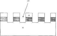
1.在半导体衬底(例如本征硅衬底11)上,通过离子注入,形成具有重掺杂层的夹层结构,其中,所述重掺杂层为夹层,如图1A所示。在本实施例中,所形成的重掺杂层为n型重掺杂层12,掺杂原子种类为磷,其上为本征硅13(原属于本征硅衬底11的一部分)。 1. On a semiconductor substrate (such as an intrinsic silicon substrate 11 ), form a sandwich structure with a heavily doped layer by ion implantation, wherein the heavily doped layer is an interlayer, as shown in FIG. 1A . In this embodiment, the formed heavily doped layer is an n-type heavily doped layer 12 , the dopant atom species is phosphorus, and the intrinsic silicon 13 (originally a part of the intrinsic silicon substrate 11 ) is formed thereon. the
2.对所述夹层结构进行光刻以形成分离的第一线阵,其中,光刻的深度超过所述重掺杂层12,如图1B所示,所述第一线阵可作为字线或位线,其包含的各线通过浅沟道4分隔开。 2. Perform photolithography on the sandwich structure to form a separate first line array, wherein the depth of the photolithography exceeds the heavily doped layer 12, as shown in FIG. 1B, the first line array can be used as a word line or bit lines, which contain individual lines separated by shallow trenches 4 . the
3.在所述第一线阵根部形成多个重掺杂的区域15,以便电学隔离所述第一线阵,使各线之间相互不导通,因此信号不受干扰,如图1C所示。 3. Form a plurality of heavily doped regions 15 at the root of the first line array, so as to electrically isolate the first line array, so that the lines are not electrically connected to each other, so the signal is not disturbed, as shown in Figure 1C Show. the
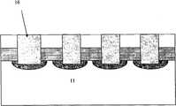
4.在形成了重掺杂的结构上采用化学气相沉积法沉积绝缘材料,并通过化学机械抛光法及平坦化操作使所述绝缘材料填充在所述第一线阵中,本实施例中,采用氧化硅作为绝缘材料形成氧化硅层16,如图1D所示。 4. On the heavily doped structure, an insulating material is deposited by chemical vapor deposition, and the insulating material is filled in the first line array by chemical mechanical polishing and planarization operations. In this embodiment, A
5.对填充了绝缘材料的结构进行离子注入,使处于表面的半导体材料(即本征硅13)轻度掺杂形成轻度掺杂层17,本实施例中离子注入的为磷原子,轻度掺杂,形成如图1E的结构。 5. Ion implantation is carried out to the structure filled with insulating material, so that the semiconductor material (i.e. intrinsic silicon 13) on the surface is slightly doped to form a lightly doped
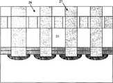
6.在所述轻度掺杂层17上覆盖半导体材料(如本征硅)并用光刻工艺刻蚀出多个第一窗口,并在各第一窗口中填充能与所述轻度掺杂层形成肖特基势垒的金属材料,以形成各金属电极18,其中,各第一窗口都处于所述轻度掺杂层17上,如图1F所示,所采用的金属材料为W,也可是Al、Cu、Mo、Ni、Ti或Pt等。 6. Cover the semiconductor material (such as intrinsic silicon) on the lightly doped
7.在具有金属电极18的结构上沉积绝缘材料,并用光刻工艺刻蚀出多个第二窗口19,其中,各第二窗口分别处于相应金属电极上方,如图1G所示,一个第一窗口上仅有一个较宽的第二窗口。 7. Deposit an insulating material on the structure with the
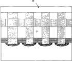
8.在各第二窗口19内依次沉积过渡性材料Pt110、相变材料GST111和金属W 112作为相变存储器电极,如图1H所示。需注意的是,相变材料也可是SiSbTe、SiSe、SiSb等材料。 8. Deposit transition material Pt110, phase change material GST111 and metal W112 in sequence in each second window 19 as phase change memory electrodes, as shown in FIG. 1H. It should be noted that the phase change material can also be SiSbTe, SiSe, SiSb and other materials. the
9.在形成了相变存储器电极的结构上沉积Al金属层113,以形成第二线阵,如图1I所示。 9. Depositing an Al metal layer 113 on the structure where the electrodes of the phase change memory are formed to form a second line array, as shown in FIG. 1I . the
实施例2: Example 2:
请参见图2A-2E,本发明的共用金属层的肖特基二极管和相变存储器阵列制造方法包括以下步骤:Please refer to FIGS. 2A-2E , the Schottky diode and phase-change memory array manufacturing method sharing a metal layer of the present invention includes the following steps:
1.按照实施例1中1-7步骤形成金属电极21,氧化硅层22,如图2A所示。 1. Form the
2.用光刻工艺在氧化硅层22刻蚀出第二窗口23,如图2B所示,即一个第一窗口上有两个较窄的第二窗口。 2. The second window 23 is etched in the
3.在第二窗口23中沉积相变材料层24,并在相变材料层24上覆盖金属25,如图2C所示。 3. Deposit a phase-
4.刻蚀金属25,形成相变存储器电极26,并填充氧化硅27,如图2D所示 4. Etching
5.沉积金属Cu28,形成第二线阵,如图2E所示。 5. Deposit metal Cu28 to form the second line array, as shown in FIG. 2E. the
实施例3: Example 3:
请参见图3A-3G,本发明的共用金属层的肖特基二极管和相变存储器阵列制造方法包括以下步骤:Referring to FIGS. 3A-3G , the manufacturing method of Schottky diodes and phase-change memory arrays sharing a metal layer of the present invention includes the following steps:
a)按照实施例1中1-5步骤形成金属电极31,如图3A。 a) Form the
b)在形成了金属电极31的结构上沉积能影响相变材料的过渡层32(如图3B),并用光刻工艺刻蚀出多个过渡层窗口33以形成相互隔离的过渡区域,并使每一金属电极31上都存在过渡区域(如图3C),再在各过渡层窗口33中填充绝缘材料(如氧化硅)34(如图3D),所述过渡层所采用的材料可为能提高相变材料的结晶速率、降低相变材料熔点的加热材料、能提高热效率的材料、或能提高加热效率、降低操作电压、抑制相变材料中Sb和Te向底电极扩散的材料等,其中,所述加热材料可为ZrO2、HfO2、Ta2O5、或TiO2等,所述能提高热效率的材料可为Pt、Ti、或TiN等;所述能降低操作电压的材料可为LaNiO3、LaSrCoO3、LaSrMnO3、SrRuO3、CaRuO3、或GeSiN等。 b) Deposit a
c)在填充了绝缘材料的结构上沉积相变材料,并刻蚀以形成多个相变材料区35,其中,每一相变材料区35处于至少一个过渡区域之上、且该过渡区域位于一金属电极上,如图3E,本实施例中,相变材料区35堆叠在两个过渡区域上,其中一个过渡区域不处于金属电极上。 c) Depositing a phase change material on the structure filled with insulating material, and etching to form a plurality of phase
d)在形成了相变材料区的结构上沉积绝缘材料以便覆盖所沉积的相变材料(如图3F),并对其进行刻蚀后填充金属材料以形成相变存储器的上电极36,如图3G,每一上电极也处于一过渡区域上,但该过渡区域不在金属电极上。 d) Deposit an insulating material on the structure where the phase change material region is formed so as to cover the deposited phase change material (as shown in FIG. 3F ), and etch it and fill it with a metal material to form the
需要说明的是,本领域的技术人员也可参照申请号为200810041393.5、200510030637.6、200810034940.7、200610028107.2、200810033601.7、200710043924.X、200410053752.0、200310109372.X、200710044609.9、及200910045816.5的各中国专利所公开相变存储器两电极之间的层级结构,对上述各实施例中形成相变存储器的步骤进行相应的调整,以实现相变存储器和肖特基二极管的金属层共享。 需要说明的是,本领域的技术人员也可参照申请号为200810041393.5、200510030637.6、200810034940.7、200610028107.2、200810033601.7、200710043924.X、200410053752.0、200310109372.X、200710044609.9、及200910045816.5的各中国专利所公开相变存储器两For the hierarchical structure between the electrodes, corresponding adjustments are made to the steps of forming the phase-change memory in the above-mentioned embodiments, so as to realize the sharing of metal layers between the phase-change memory and the Schottky diode. the
综上所述,本发明的共用金属层的肖特基二极管和相变存储器阵列制造方法将作为肖特基二极管的金属层又作为相变存储器结构的下电极,即可实现金属层的共享,可以有较少的工艺步骤制造了二极管和相变存储器阵列,有效节省了光刻次数,通过采用特定的半导体,使得电极金属和半导体层之间形成稳定的肖特基接触。 In summary, the method for manufacturing the Schottky diode and the phase change memory array sharing the metal layer of the present invention uses the metal layer of the Schottky diode as the lower electrode of the phase change memory structure, so that the sharing of the metal layer can be realized. The diode and the phase-change memory array can be manufactured with fewer process steps, which effectively saves the number of photolithography times. By using a specific semiconductor, a stable Schottky contact is formed between the electrode metal and the semiconductor layer. the
上述实施例仅列示性说明本发明的原理及功效,而非用于限制本发明。任何熟悉此项技术的人员均可在不违背本发明的精神及范围下,对上述实施例进行修改。因此,本发明的权 利保护范围,应如权利要求书所列。 The above-mentioned embodiments only illustrate the principles and functions of the present invention, but are not intended to limit the present invention. Anyone skilled in the art can make modifications to the above-mentioned embodiments without departing from the spirit and scope of the present invention. Therefore, the protection scope of the present invention should be as listed in the claims. the
Claims (6)
Translated fromChinesePriority Applications (1)
| Application Number | Priority Date | Filing Date | Title |
|---|---|---|---|
| CN2010101381676ACN101826463B (en) | 2010-04-01 | 2010-04-01 | Manufacturing method of Schottky diode and phase-change memory with shared metal layer |
Applications Claiming Priority (1)
| Application Number | Priority Date | Filing Date | Title |
|---|---|---|---|
| CN2010101381676ACN101826463B (en) | 2010-04-01 | 2010-04-01 | Manufacturing method of Schottky diode and phase-change memory with shared metal layer |
Publications (2)
| Publication Number | Publication Date |
|---|---|
| CN101826463A CN101826463A (en) | 2010-09-08 |
| CN101826463Btrue CN101826463B (en) | 2012-02-29 |
Family
ID=42690302
Family Applications (1)
| Application Number | Title | Priority Date | Filing Date |
|---|---|---|---|
| CN2010101381676AExpired - Fee RelatedCN101826463B (en) | 2010-04-01 | 2010-04-01 | Manufacturing method of Schottky diode and phase-change memory with shared metal layer |
Country Status (1)
| Country | Link |
|---|---|
| CN (1) | CN101826463B (en) |
Families Citing this family (1)
| Publication number | Priority date | Publication date | Assignee | Title |
|---|---|---|---|---|
| CN109686755B (en)* | 2018-12-26 | 2022-07-05 | 上海集成电路研发中心有限公司 | High-density phase change memory and preparation method thereof |
Family Cites Families (3)
| Publication number | Priority date | Publication date | Assignee | Title |
|---|---|---|---|---|
| US7767993B2 (en)* | 2002-04-04 | 2010-08-03 | Kabushiki Kaisha Toshiba | Resistance change memory device |
| CN100550409C (en)* | 2007-06-21 | 2009-10-14 | 复旦大学 | Phase transition storage and manufacture method thereof based on the diode gating |
| CN101436614B (en)* | 2008-12-19 | 2011-05-11 | 中国科学院上海微系统与信息技术研究所 | self-aligning manufacturing method for antimonous schottky diode |
- 2010
- 2010-04-01CNCN2010101381676Apatent/CN101826463B/ennot_activeExpired - Fee Related
Also Published As
| Publication number | Publication date |
|---|---|
| CN101826463A (en) | 2010-09-08 |
Similar Documents
| Publication | Publication Date | Title |
|---|---|---|
| US11043537B2 (en) | Three-dimensional phase change memory device including vertically constricted current paths and methods of manufacturing the same | |
| US10964752B2 (en) | Three-dimensional memory device including laterally constricted current paths and methods of manufacturing the same | |
| TWI609513B (en) | Array of cross point memory cells and methods of forming an array of cross point memory cells | |
| US9276202B2 (en) | Phase-change storage unit containing TiSiN material layer and method for preparing the same | |
| US7220983B2 (en) | Self-aligned small contact phase-change memory method and device | |
| US10868245B1 (en) | Phase change memory device with crystallization template and method of making the same | |
| US8288752B2 (en) | Phase change memory device capable of reducing disturbance and method of manufacturing the same | |
| CN105428526B (en) | A kind of three-dimensional storage and preparation method thereof | |
| KR100985756B1 (en) | Phase change memory device and manufacturing method thereof | |
| JP2010123664A (en) | Nonvolatile memory device | |
| CN101477987A (en) | Tri-dimension stacked resistance conversion memory and manufacturing process thereof | |
| US8853044B2 (en) | Phase-change random access memory device and method of manufacturing the same | |
| US20150188041A1 (en) | Phase-Change Storage Unit For Replacing DRAM And FLASH And Manufacturing Method Thereof | |
| JP2009206418A (en) | Nonvolatile memory device and manufacturing method for the same | |
| CN110858623B (en) | Variable resistance memory device and method of manufacturing the same | |
| CN111029362B (en) | A method for preparing a high-density phase-change memory three-dimensional integrated circuit structure | |
| CN102064276A (en) | Asymmetric phase-change memory unit and element | |
| CN113330594B (en) | Switching device with bidirectional driving characteristics and operation method thereof | |
| CN101976677B (en) | ZnO Schottky diode-based phase-change random access memory array and manufacturing method | |
| CN101826463B (en) | Manufacturing method of Schottky diode and phase-change memory with shared metal layer | |
| CN103325940B (en) | Phase-change memory cell and manufacturing method thereof | |
| CN105633279A (en) | Phase-change memory unit comprising partially defined phase-change material structures and fabrication method | |
| CN101661992B (en) | Combined electrode structure of phase change memory cell device | |
| KR100701157B1 (en) | Non-volatile memory device comprising a phase change material and a manufacturing method | |
| CN107819070B (en) | Preparation method of phase change memory with 1D1R superconducting electrode material structure |
Legal Events
| Date | Code | Title | Description |
|---|---|---|---|
| C06 | Publication | ||
| PB01 | Publication | ||
| C10 | Entry into substantive examination | ||
| SE01 | Entry into force of request for substantive examination | ||
| C14 | Grant of patent or utility model | ||
| GR01 | Patent grant | ||
| CF01 | Termination of patent right due to non-payment of annual fee | ||
| CF01 | Termination of patent right due to non-payment of annual fee | Granted publication date:20120229 |