CN101821833A - Method for manufacturing semiconductor chip with adhesive film, adhesive film for semiconductor used for the manufacturing method, and method for manufacturing semiconductor device - Google Patents
Method for manufacturing semiconductor chip with adhesive film, adhesive film for semiconductor used for the manufacturing method, and method for manufacturing semiconductor deviceDownload PDFInfo
- Publication number
- CN101821833A CN101821833ACN200880110812ACN200880110812ACN101821833ACN 101821833 ACN101821833 ACN 101821833ACN 200880110812 ACN200880110812 ACN 200880110812ACN 200880110812 ACN200880110812 ACN 200880110812ACN 101821833 ACN101821833 ACN 101821833A
- Authority
- CN
- China
- Prior art keywords
- semiconductor
- adhesive film
- semiconductor chip
- film
- semiconductor wafer
- Prior art date
- Legal status (The legal status is an assumption and is not a legal conclusion. Google has not performed a legal analysis and makes no representation as to the accuracy of the status listed.)
- Granted
Links
Images

Classifications
- H—ELECTRICITY
- H01—ELECTRIC ELEMENTS
- H01L—SEMICONDUCTOR DEVICES NOT COVERED BY CLASS H10
- H01L21/00—Processes or apparatus adapted for the manufacture or treatment of semiconductor or solid state devices or of parts thereof
- H01L21/67—Apparatus specially adapted for handling semiconductor or electric solid state devices during manufacture or treatment thereof; Apparatus specially adapted for handling wafers during manufacture or treatment of semiconductor or electric solid state devices or components ; Apparatus not specifically provided for elsewhere
- H01L21/67005—Apparatus not specifically provided for elsewhere
- H01L21/67011—Apparatus for manufacture or treatment
- H01L21/67132—Apparatus for placing on an insulating substrate, e.g. tape
- H—ELECTRICITY
- H01—ELECTRIC ELEMENTS
- H01L—SEMICONDUCTOR DEVICES NOT COVERED BY CLASS H10
- H01L21/00—Processes or apparatus adapted for the manufacture or treatment of semiconductor or solid state devices or of parts thereof
- H01L21/02—Manufacture or treatment of semiconductor devices or of parts thereof
- H01L21/04—Manufacture or treatment of semiconductor devices or of parts thereof the devices having potential barriers, e.g. a PN junction, depletion layer or carrier concentration layer
- H01L21/18—Manufacture or treatment of semiconductor devices or of parts thereof the devices having potential barriers, e.g. a PN junction, depletion layer or carrier concentration layer the devices having semiconductor bodies comprising elements of Group IV of the Periodic Table or AIIIBV compounds with or without impurities, e.g. doping materials
- H01L21/30—Treatment of semiconductor bodies using processes or apparatus not provided for in groups H01L21/20 - H01L21/26
- B—PERFORMING OPERATIONS; TRANSPORTING
- B23—MACHINE TOOLS; METAL-WORKING NOT OTHERWISE PROVIDED FOR
- B23K—SOLDERING OR UNSOLDERING; WELDING; CLADDING OR PLATING BY SOLDERING OR WELDING; CUTTING BY APPLYING HEAT LOCALLY, e.g. FLAME CUTTING; WORKING BY LASER BEAM
- B23K26/00—Working by laser beam, e.g. welding, cutting or boring
- B23K26/36—Removing material
- B23K26/40—Removing material taking account of the properties of the material involved
- B—PERFORMING OPERATIONS; TRANSPORTING
- B23—MACHINE TOOLS; METAL-WORKING NOT OTHERWISE PROVIDED FOR
- B23K—SOLDERING OR UNSOLDERING; WELDING; CLADDING OR PLATING BY SOLDERING OR WELDING; CUTTING BY APPLYING HEAT LOCALLY, e.g. FLAME CUTTING; WORKING BY LASER BEAM
- B23K26/00—Working by laser beam, e.g. welding, cutting or boring
- B23K26/50—Working by transmitting the laser beam through or within the workpiece
- B23K26/53—Working by transmitting the laser beam through or within the workpiece for modifying or reforming the material inside the workpiece, e.g. for producing break initiation cracks
- B—PERFORMING OPERATIONS; TRANSPORTING
- B28—WORKING CEMENT, CLAY, OR STONE
- B28D—WORKING STONE OR STONE-LIKE MATERIALS
- B28D5/00—Fine working of gems, jewels, crystals, e.g. of semiconductor material; apparatus or devices therefor
- B28D5/0005—Fine working of gems, jewels, crystals, e.g. of semiconductor material; apparatus or devices therefor by breaking, e.g. dicing
- B28D5/0011—Fine working of gems, jewels, crystals, e.g. of semiconductor material; apparatus or devices therefor by breaking, e.g. dicing with preliminary treatment, e.g. weakening by scoring
- B—PERFORMING OPERATIONS; TRANSPORTING
- B28—WORKING CEMENT, CLAY, OR STONE
- B28D—WORKING STONE OR STONE-LIKE MATERIALS
- B28D5/00—Fine working of gems, jewels, crystals, e.g. of semiconductor material; apparatus or devices therefor
- B28D5/0005—Fine working of gems, jewels, crystals, e.g. of semiconductor material; apparatus or devices therefor by breaking, e.g. dicing
- B28D5/0052—Means for supporting or holding work during breaking
- H—ELECTRICITY
- H01—ELECTRIC ELEMENTS
- H01L—SEMICONDUCTOR DEVICES NOT COVERED BY CLASS H10
- H01L21/00—Processes or apparatus adapted for the manufacture or treatment of semiconductor or solid state devices or of parts thereof
- H01L21/02—Manufacture or treatment of semiconductor devices or of parts thereof
- H01L21/04—Manufacture or treatment of semiconductor devices or of parts thereof the devices having potential barriers, e.g. a PN junction, depletion layer or carrier concentration layer
- H01L21/50—Assembly of semiconductor devices using processes or apparatus not provided for in a single one of the groups H01L21/18 - H01L21/326 or H10D48/04 - H10D48/07 e.g. sealing of a cap to a base of a container
- H01L21/52—Mounting semiconductor bodies in containers
- H—ELECTRICITY
- H01—ELECTRIC ELEMENTS
- H01L—SEMICONDUCTOR DEVICES NOT COVERED BY CLASS H10
- H01L21/00—Processes or apparatus adapted for the manufacture or treatment of semiconductor or solid state devices or of parts thereof
- H01L21/67—Apparatus specially adapted for handling semiconductor or electric solid state devices during manufacture or treatment thereof; Apparatus specially adapted for handling wafers during manufacture or treatment of semiconductor or electric solid state devices or components ; Apparatus not specifically provided for elsewhere
- H01L21/683—Apparatus specially adapted for handling semiconductor or electric solid state devices during manufacture or treatment thereof; Apparatus specially adapted for handling wafers during manufacture or treatment of semiconductor or electric solid state devices or components ; Apparatus not specifically provided for elsewhere for supporting or gripping
- H01L21/6835—Apparatus specially adapted for handling semiconductor or electric solid state devices during manufacture or treatment thereof; Apparatus specially adapted for handling wafers during manufacture or treatment of semiconductor or electric solid state devices or components ; Apparatus not specifically provided for elsewhere for supporting or gripping using temporarily an auxiliary support
- H01L21/6836—Wafer tapes, e.g. grinding or dicing support tapes
- H—ELECTRICITY
- H01—ELECTRIC ELEMENTS
- H01L—SEMICONDUCTOR DEVICES NOT COVERED BY CLASS H10
- H01L21/00—Processes or apparatus adapted for the manufacture or treatment of semiconductor or solid state devices or of parts thereof
- H01L21/70—Manufacture or treatment of devices consisting of a plurality of solid state components formed in or on a common substrate or of parts thereof; Manufacture of integrated circuit devices or of parts thereof
- H01L21/77—Manufacture or treatment of devices consisting of a plurality of solid state components or integrated circuits formed in, or on, a common substrate
- H01L21/78—Manufacture or treatment of devices consisting of a plurality of solid state components or integrated circuits formed in, or on, a common substrate with subsequent division of the substrate into plural individual devices
- H—ELECTRICITY
- H01—ELECTRIC ELEMENTS
- H01L—SEMICONDUCTOR DEVICES NOT COVERED BY CLASS H10
- H01L23/00—Details of semiconductor or other solid state devices
- H01L23/28—Encapsulations, e.g. encapsulating layers, coatings, e.g. for protection
- H01L23/31—Encapsulations, e.g. encapsulating layers, coatings, e.g. for protection characterised by the arrangement or shape
- H01L23/3107—Encapsulations, e.g. encapsulating layers, coatings, e.g. for protection characterised by the arrangement or shape the device being completely enclosed
- H01L23/3121—Encapsulations, e.g. encapsulating layers, coatings, e.g. for protection characterised by the arrangement or shape the device being completely enclosed a substrate forming part of the encapsulation
- H—ELECTRICITY
- H01—ELECTRIC ELEMENTS
- H01L—SEMICONDUCTOR DEVICES NOT COVERED BY CLASS H10
- H01L24/00—Arrangements for connecting or disconnecting semiconductor or solid-state bodies; Methods or apparatus related thereto
- H01L24/01—Means for bonding being attached to, or being formed on, the surface to be connected, e.g. chip-to-package, die-attach, "first-level" interconnects; Manufacturing methods related thereto
- H01L24/26—Layer connectors, e.g. plate connectors, solder or adhesive layers; Manufacturing methods related thereto
- H01L24/27—Manufacturing methods
- H—ELECTRICITY
- H01—ELECTRIC ELEMENTS
- H01L—SEMICONDUCTOR DEVICES NOT COVERED BY CLASS H10
- H01L24/00—Arrangements for connecting or disconnecting semiconductor or solid-state bodies; Methods or apparatus related thereto
- H01L24/01—Means for bonding being attached to, or being formed on, the surface to be connected, e.g. chip-to-package, die-attach, "first-level" interconnects; Manufacturing methods related thereto
- H01L24/26—Layer connectors, e.g. plate connectors, solder or adhesive layers; Manufacturing methods related thereto
- H01L24/28—Structure, shape, material or disposition of the layer connectors prior to the connecting process
- H01L24/29—Structure, shape, material or disposition of the layer connectors prior to the connecting process of an individual layer connector
- H—ELECTRICITY
- H01—ELECTRIC ELEMENTS
- H01L—SEMICONDUCTOR DEVICES NOT COVERED BY CLASS H10
- H01L24/00—Arrangements for connecting or disconnecting semiconductor or solid-state bodies; Methods or apparatus related thereto
- H01L24/80—Methods for connecting semiconductor or other solid state bodies using means for bonding being attached to, or being formed on, the surface to be connected
- H01L24/83—Methods for connecting semiconductor or other solid state bodies using means for bonding being attached to, or being formed on, the surface to be connected using a layer connector
- B—PERFORMING OPERATIONS; TRANSPORTING
- B23—MACHINE TOOLS; METAL-WORKING NOT OTHERWISE PROVIDED FOR
- B23K—SOLDERING OR UNSOLDERING; WELDING; CLADDING OR PLATING BY SOLDERING OR WELDING; CUTTING BY APPLYING HEAT LOCALLY, e.g. FLAME CUTTING; WORKING BY LASER BEAM
- B23K2101/00—Articles made by soldering, welding or cutting
- B23K2101/36—Electric or electronic devices
- B23K2101/40—Semiconductor devices
- B—PERFORMING OPERATIONS; TRANSPORTING
- B23—MACHINE TOOLS; METAL-WORKING NOT OTHERWISE PROVIDED FOR
- B23K—SOLDERING OR UNSOLDERING; WELDING; CLADDING OR PLATING BY SOLDERING OR WELDING; CUTTING BY APPLYING HEAT LOCALLY, e.g. FLAME CUTTING; WORKING BY LASER BEAM
- B23K2103/00—Materials to be soldered, welded or cut
- B23K2103/50—Inorganic material, e.g. metals, not provided for in B23K2103/02 – B23K2103/26
- H—ELECTRICITY
- H01—ELECTRIC ELEMENTS
- H01L—SEMICONDUCTOR DEVICES NOT COVERED BY CLASS H10
- H01L2221/00—Processes or apparatus adapted for the manufacture or treatment of semiconductor or solid state devices or of parts thereof covered by H01L21/00
- H01L2221/67—Apparatus for handling semiconductor or electric solid state devices during manufacture or treatment thereof; Apparatus for handling wafers during manufacture or treatment of semiconductor or electric solid state devices or components; Apparatus not specifically provided for elsewhere
- H01L2221/683—Apparatus for handling semiconductor or electric solid state devices during manufacture or treatment thereof; Apparatus for handling wafers during manufacture or treatment of semiconductor or electric solid state devices or components; Apparatus not specifically provided for elsewhere for supporting or gripping
- H01L2221/68304—Apparatus for handling semiconductor or electric solid state devices during manufacture or treatment thereof; Apparatus for handling wafers during manufacture or treatment of semiconductor or electric solid state devices or components; Apparatus not specifically provided for elsewhere for supporting or gripping using temporarily an auxiliary support
- H01L2221/68327—Apparatus for handling semiconductor or electric solid state devices during manufacture or treatment thereof; Apparatus for handling wafers during manufacture or treatment of semiconductor or electric solid state devices or components; Apparatus not specifically provided for elsewhere for supporting or gripping using temporarily an auxiliary support used during dicing or grinding
- H01L2221/68336—Apparatus for handling semiconductor or electric solid state devices during manufacture or treatment thereof; Apparatus for handling wafers during manufacture or treatment of semiconductor or electric solid state devices or components; Apparatus not specifically provided for elsewhere for supporting or gripping using temporarily an auxiliary support used during dicing or grinding involving stretching of the auxiliary support post dicing
- H—ELECTRICITY
- H01—ELECTRIC ELEMENTS
- H01L—SEMICONDUCTOR DEVICES NOT COVERED BY CLASS H10
- H01L2224/00—Indexing scheme for arrangements for connecting or disconnecting semiconductor or solid-state bodies and methods related thereto as covered by H01L24/00
- H01L2224/01—Means for bonding being attached to, or being formed on, the surface to be connected, e.g. chip-to-package, die-attach, "first-level" interconnects; Manufacturing methods related thereto
- H01L2224/26—Layer connectors, e.g. plate connectors, solder or adhesive layers; Manufacturing methods related thereto
- H01L2224/27—Manufacturing methods
- H01L2224/274—Manufacturing methods by blanket deposition of the material of the layer connector
- H—ELECTRICITY
- H01—ELECTRIC ELEMENTS
- H01L—SEMICONDUCTOR DEVICES NOT COVERED BY CLASS H10
- H01L2224/00—Indexing scheme for arrangements for connecting or disconnecting semiconductor or solid-state bodies and methods related thereto as covered by H01L24/00
- H01L2224/01—Means for bonding being attached to, or being formed on, the surface to be connected, e.g. chip-to-package, die-attach, "first-level" interconnects; Manufacturing methods related thereto
- H01L2224/26—Layer connectors, e.g. plate connectors, solder or adhesive layers; Manufacturing methods related thereto
- H01L2224/28—Structure, shape, material or disposition of the layer connectors prior to the connecting process
- H01L2224/29—Structure, shape, material or disposition of the layer connectors prior to the connecting process of an individual layer connector
- H01L2224/29001—Core members of the layer connector
- H01L2224/29099—Material
- H01L2224/2919—Material with a principal constituent of the material being a polymer, e.g. polyester, phenolic based polymer, epoxy
- H—ELECTRICITY
- H01—ELECTRIC ELEMENTS
- H01L—SEMICONDUCTOR DEVICES NOT COVERED BY CLASS H10
- H01L2224/00—Indexing scheme for arrangements for connecting or disconnecting semiconductor or solid-state bodies and methods related thereto as covered by H01L24/00
- H01L2224/01—Means for bonding being attached to, or being formed on, the surface to be connected, e.g. chip-to-package, die-attach, "first-level" interconnects; Manufacturing methods related thereto
- H01L2224/26—Layer connectors, e.g. plate connectors, solder or adhesive layers; Manufacturing methods related thereto
- H01L2224/31—Structure, shape, material or disposition of the layer connectors after the connecting process
- H01L2224/32—Structure, shape, material or disposition of the layer connectors after the connecting process of an individual layer connector
- H01L2224/321—Disposition
- H01L2224/32151—Disposition the layer connector connecting between a semiconductor or solid-state body and an item not being a semiconductor or solid-state body, e.g. chip-to-substrate, chip-to-passive
- H01L2224/32221—Disposition the layer connector connecting between a semiconductor or solid-state body and an item not being a semiconductor or solid-state body, e.g. chip-to-substrate, chip-to-passive the body and the item being stacked
- H01L2224/32225—Disposition the layer connector connecting between a semiconductor or solid-state body and an item not being a semiconductor or solid-state body, e.g. chip-to-substrate, chip-to-passive the body and the item being stacked the item being non-metallic, e.g. insulating substrate with or without metallisation
- H—ELECTRICITY
- H01—ELECTRIC ELEMENTS
- H01L—SEMICONDUCTOR DEVICES NOT COVERED BY CLASS H10
- H01L2224/00—Indexing scheme for arrangements for connecting or disconnecting semiconductor or solid-state bodies and methods related thereto as covered by H01L24/00
- H01L2224/01—Means for bonding being attached to, or being formed on, the surface to be connected, e.g. chip-to-package, die-attach, "first-level" interconnects; Manufacturing methods related thereto
- H01L2224/42—Wire connectors; Manufacturing methods related thereto
- H01L2224/47—Structure, shape, material or disposition of the wire connectors after the connecting process
- H01L2224/48—Structure, shape, material or disposition of the wire connectors after the connecting process of an individual wire connector
- H01L2224/4805—Shape
- H01L2224/4809—Loop shape
- H01L2224/48091—Arched
- H—ELECTRICITY
- H01—ELECTRIC ELEMENTS
- H01L—SEMICONDUCTOR DEVICES NOT COVERED BY CLASS H10
- H01L2224/00—Indexing scheme for arrangements for connecting or disconnecting semiconductor or solid-state bodies and methods related thereto as covered by H01L24/00
- H01L2224/01—Means for bonding being attached to, or being formed on, the surface to be connected, e.g. chip-to-package, die-attach, "first-level" interconnects; Manufacturing methods related thereto
- H01L2224/42—Wire connectors; Manufacturing methods related thereto
- H01L2224/47—Structure, shape, material or disposition of the wire connectors after the connecting process
- H01L2224/48—Structure, shape, material or disposition of the wire connectors after the connecting process of an individual wire connector
- H01L2224/481—Disposition
- H01L2224/48151—Connecting between a semiconductor or solid-state body and an item not being a semiconductor or solid-state body, e.g. chip-to-substrate, chip-to-passive
- H01L2224/48221—Connecting between a semiconductor or solid-state body and an item not being a semiconductor or solid-state body, e.g. chip-to-substrate, chip-to-passive the body and the item being stacked
- H01L2224/48225—Connecting between a semiconductor or solid-state body and an item not being a semiconductor or solid-state body, e.g. chip-to-substrate, chip-to-passive the body and the item being stacked the item being non-metallic, e.g. insulating substrate with or without metallisation
- H01L2224/48227—Connecting between a semiconductor or solid-state body and an item not being a semiconductor or solid-state body, e.g. chip-to-substrate, chip-to-passive the body and the item being stacked the item being non-metallic, e.g. insulating substrate with or without metallisation connecting the wire to a bond pad of the item
- H—ELECTRICITY
- H01—ELECTRIC ELEMENTS
- H01L—SEMICONDUCTOR DEVICES NOT COVERED BY CLASS H10
- H01L2224/00—Indexing scheme for arrangements for connecting or disconnecting semiconductor or solid-state bodies and methods related thereto as covered by H01L24/00
- H01L2224/73—Means for bonding being of different types provided for in two or more of groups H01L2224/10, H01L2224/18, H01L2224/26, H01L2224/34, H01L2224/42, H01L2224/50, H01L2224/63, H01L2224/71
- H01L2224/732—Location after the connecting process
- H01L2224/73251—Location after the connecting process on different surfaces
- H01L2224/73265—Layer and wire connectors
- H—ELECTRICITY
- H01—ELECTRIC ELEMENTS
- H01L—SEMICONDUCTOR DEVICES NOT COVERED BY CLASS H10
- H01L2224/00—Indexing scheme for arrangements for connecting or disconnecting semiconductor or solid-state bodies and methods related thereto as covered by H01L24/00
- H01L2224/80—Methods for connecting semiconductor or other solid state bodies using means for bonding being attached to, or being formed on, the surface to be connected
- H01L2224/83—Methods for connecting semiconductor or other solid state bodies using means for bonding being attached to, or being formed on, the surface to be connected using a layer connector
- H01L2224/8319—Arrangement of the layer connectors prior to mounting
- H01L2224/83191—Arrangement of the layer connectors prior to mounting wherein the layer connectors are disposed only on the semiconductor or solid-state body
- H—ELECTRICITY
- H01—ELECTRIC ELEMENTS
- H01L—SEMICONDUCTOR DEVICES NOT COVERED BY CLASS H10
- H01L2224/00—Indexing scheme for arrangements for connecting or disconnecting semiconductor or solid-state bodies and methods related thereto as covered by H01L24/00
- H01L2224/80—Methods for connecting semiconductor or other solid state bodies using means for bonding being attached to, or being formed on, the surface to be connected
- H01L2224/83—Methods for connecting semiconductor or other solid state bodies using means for bonding being attached to, or being formed on, the surface to be connected using a layer connector
- H01L2224/838—Bonding techniques
- H01L2224/8385—Bonding techniques using a polymer adhesive, e.g. an adhesive based on silicone, epoxy, polyimide, polyester
- H01L2224/83855—Hardening the adhesive by curing, i.e. thermosetting
- H—ELECTRICITY
- H01—ELECTRIC ELEMENTS
- H01L—SEMICONDUCTOR DEVICES NOT COVERED BY CLASS H10
- H01L2224/00—Indexing scheme for arrangements for connecting or disconnecting semiconductor or solid-state bodies and methods related thereto as covered by H01L24/00
- H01L2224/80—Methods for connecting semiconductor or other solid state bodies using means for bonding being attached to, or being formed on, the surface to be connected
- H01L2224/83—Methods for connecting semiconductor or other solid state bodies using means for bonding being attached to, or being formed on, the surface to be connected using a layer connector
- H01L2224/838—Bonding techniques
- H01L2224/8385—Bonding techniques using a polymer adhesive, e.g. an adhesive based on silicone, epoxy, polyimide, polyester
- H01L2224/8388—Hardening the adhesive by cooling, e.g. for thermoplastics or hot-melt adhesives
- H—ELECTRICITY
- H01—ELECTRIC ELEMENTS
- H01L—SEMICONDUCTOR DEVICES NOT COVERED BY CLASS H10
- H01L2224/00—Indexing scheme for arrangements for connecting or disconnecting semiconductor or solid-state bodies and methods related thereto as covered by H01L24/00
- H01L2224/80—Methods for connecting semiconductor or other solid state bodies using means for bonding being attached to, or being formed on, the surface to be connected
- H01L2224/83—Methods for connecting semiconductor or other solid state bodies using means for bonding being attached to, or being formed on, the surface to be connected using a layer connector
- H01L2224/838—Bonding techniques
- H01L2224/8385—Bonding techniques using a polymer adhesive, e.g. an adhesive based on silicone, epoxy, polyimide, polyester
- H01L2224/83885—Combinations of two or more hardening methods provided for in at least two different groups from H01L2224/83855 - H01L2224/8388, e.g. for hybrid thermoplastic-thermosetting adhesives
- H—ELECTRICITY
- H01—ELECTRIC ELEMENTS
- H01L—SEMICONDUCTOR DEVICES NOT COVERED BY CLASS H10
- H01L2224/00—Indexing scheme for arrangements for connecting or disconnecting semiconductor or solid-state bodies and methods related thereto as covered by H01L24/00
- H01L2224/91—Methods for connecting semiconductor or solid state bodies including different methods provided for in two or more of groups H01L2224/80 - H01L2224/90
- H01L2224/92—Specific sequence of method steps
- H01L2224/922—Connecting different surfaces of the semiconductor or solid-state body with connectors of different types
- H01L2224/9222—Sequential connecting processes
- H01L2224/92242—Sequential connecting processes the first connecting process involving a layer connector
- H01L2224/92247—Sequential connecting processes the first connecting process involving a layer connector the second connecting process involving a wire connector
- H—ELECTRICITY
- H01—ELECTRIC ELEMENTS
- H01L—SEMICONDUCTOR DEVICES NOT COVERED BY CLASS H10
- H01L24/00—Arrangements for connecting or disconnecting semiconductor or solid-state bodies; Methods or apparatus related thereto
- H01L24/01—Means for bonding being attached to, or being formed on, the surface to be connected, e.g. chip-to-package, die-attach, "first-level" interconnects; Manufacturing methods related thereto
- H01L24/42—Wire connectors; Manufacturing methods related thereto
- H01L24/47—Structure, shape, material or disposition of the wire connectors after the connecting process
- H01L24/48—Structure, shape, material or disposition of the wire connectors after the connecting process of an individual wire connector
- H—ELECTRICITY
- H01—ELECTRIC ELEMENTS
- H01L—SEMICONDUCTOR DEVICES NOT COVERED BY CLASS H10
- H01L24/00—Arrangements for connecting or disconnecting semiconductor or solid-state bodies; Methods or apparatus related thereto
- H01L24/73—Means for bonding being of different types provided for in two or more of groups H01L24/10, H01L24/18, H01L24/26, H01L24/34, H01L24/42, H01L24/50, H01L24/63, H01L24/71
- H—ELECTRICITY
- H01—ELECTRIC ELEMENTS
- H01L—SEMICONDUCTOR DEVICES NOT COVERED BY CLASS H10
- H01L2924/00—Indexing scheme for arrangements or methods for connecting or disconnecting semiconductor or solid-state bodies as covered by H01L24/00
- H01L2924/0001—Technical content checked by a classifier
- H01L2924/00014—Technical content checked by a classifier the subject-matter covered by the group, the symbol of which is combined with the symbol of this group, being disclosed without further technical details
- H—ELECTRICITY
- H01—ELECTRIC ELEMENTS
- H01L—SEMICONDUCTOR DEVICES NOT COVERED BY CLASS H10
- H01L2924/00—Indexing scheme for arrangements or methods for connecting or disconnecting semiconductor or solid-state bodies as covered by H01L24/00
- H01L2924/01—Chemical elements
- H01L2924/01004—Beryllium [Be]
- H—ELECTRICITY
- H01—ELECTRIC ELEMENTS
- H01L—SEMICONDUCTOR DEVICES NOT COVERED BY CLASS H10
- H01L2924/00—Indexing scheme for arrangements or methods for connecting or disconnecting semiconductor or solid-state bodies as covered by H01L24/00
- H01L2924/01—Chemical elements
- H01L2924/01005—Boron [B]
- H—ELECTRICITY
- H01—ELECTRIC ELEMENTS
- H01L—SEMICONDUCTOR DEVICES NOT COVERED BY CLASS H10
- H01L2924/00—Indexing scheme for arrangements or methods for connecting or disconnecting semiconductor or solid-state bodies as covered by H01L24/00
- H01L2924/01—Chemical elements
- H01L2924/01006—Carbon [C]
- H—ELECTRICITY
- H01—ELECTRIC ELEMENTS
- H01L—SEMICONDUCTOR DEVICES NOT COVERED BY CLASS H10
- H01L2924/00—Indexing scheme for arrangements or methods for connecting or disconnecting semiconductor or solid-state bodies as covered by H01L24/00
- H01L2924/01—Chemical elements
- H01L2924/01012—Magnesium [Mg]
- H—ELECTRICITY
- H01—ELECTRIC ELEMENTS
- H01L—SEMICONDUCTOR DEVICES NOT COVERED BY CLASS H10
- H01L2924/00—Indexing scheme for arrangements or methods for connecting or disconnecting semiconductor or solid-state bodies as covered by H01L24/00
- H01L2924/01—Chemical elements
- H01L2924/01013—Aluminum [Al]
- H—ELECTRICITY
- H01—ELECTRIC ELEMENTS
- H01L—SEMICONDUCTOR DEVICES NOT COVERED BY CLASS H10
- H01L2924/00—Indexing scheme for arrangements or methods for connecting or disconnecting semiconductor or solid-state bodies as covered by H01L24/00
- H01L2924/01—Chemical elements
- H01L2924/01015—Phosphorus [P]
- H—ELECTRICITY
- H01—ELECTRIC ELEMENTS
- H01L—SEMICONDUCTOR DEVICES NOT COVERED BY CLASS H10
- H01L2924/00—Indexing scheme for arrangements or methods for connecting or disconnecting semiconductor or solid-state bodies as covered by H01L24/00
- H01L2924/01—Chemical elements
- H01L2924/01019—Potassium [K]
- H—ELECTRICITY
- H01—ELECTRIC ELEMENTS
- H01L—SEMICONDUCTOR DEVICES NOT COVERED BY CLASS H10
- H01L2924/00—Indexing scheme for arrangements or methods for connecting or disconnecting semiconductor or solid-state bodies as covered by H01L24/00
- H01L2924/01—Chemical elements
- H01L2924/0102—Calcium [Ca]
- H—ELECTRICITY
- H01—ELECTRIC ELEMENTS
- H01L—SEMICONDUCTOR DEVICES NOT COVERED BY CLASS H10
- H01L2924/00—Indexing scheme for arrangements or methods for connecting or disconnecting semiconductor or solid-state bodies as covered by H01L24/00
- H01L2924/01—Chemical elements
- H01L2924/01027—Cobalt [Co]
- H—ELECTRICITY
- H01—ELECTRIC ELEMENTS
- H01L—SEMICONDUCTOR DEVICES NOT COVERED BY CLASS H10
- H01L2924/00—Indexing scheme for arrangements or methods for connecting or disconnecting semiconductor or solid-state bodies as covered by H01L24/00
- H01L2924/01—Chemical elements
- H01L2924/01029—Copper [Cu]
- H—ELECTRICITY
- H01—ELECTRIC ELEMENTS
- H01L—SEMICONDUCTOR DEVICES NOT COVERED BY CLASS H10
- H01L2924/00—Indexing scheme for arrangements or methods for connecting or disconnecting semiconductor or solid-state bodies as covered by H01L24/00
- H01L2924/01—Chemical elements
- H01L2924/01033—Arsenic [As]
- H—ELECTRICITY
- H01—ELECTRIC ELEMENTS
- H01L—SEMICONDUCTOR DEVICES NOT COVERED BY CLASS H10
- H01L2924/00—Indexing scheme for arrangements or methods for connecting or disconnecting semiconductor or solid-state bodies as covered by H01L24/00
- H01L2924/01—Chemical elements
- H01L2924/01047—Silver [Ag]
- H—ELECTRICITY
- H01—ELECTRIC ELEMENTS
- H01L—SEMICONDUCTOR DEVICES NOT COVERED BY CLASS H10
- H01L2924/00—Indexing scheme for arrangements or methods for connecting or disconnecting semiconductor or solid-state bodies as covered by H01L24/00
- H01L2924/01—Chemical elements
- H01L2924/01051—Antimony [Sb]
- H—ELECTRICITY
- H01—ELECTRIC ELEMENTS
- H01L—SEMICONDUCTOR DEVICES NOT COVERED BY CLASS H10
- H01L2924/00—Indexing scheme for arrangements or methods for connecting or disconnecting semiconductor or solid-state bodies as covered by H01L24/00
- H01L2924/01—Chemical elements
- H01L2924/01082—Lead [Pb]
- H—ELECTRICITY
- H01—ELECTRIC ELEMENTS
- H01L—SEMICONDUCTOR DEVICES NOT COVERED BY CLASS H10
- H01L2924/00—Indexing scheme for arrangements or methods for connecting or disconnecting semiconductor or solid-state bodies as covered by H01L24/00
- H01L2924/06—Polymers
- H01L2924/0665—Epoxy resin
- H—ELECTRICITY
- H01—ELECTRIC ELEMENTS
- H01L—SEMICONDUCTOR DEVICES NOT COVERED BY CLASS H10
- H01L2924/00—Indexing scheme for arrangements or methods for connecting or disconnecting semiconductor or solid-state bodies as covered by H01L24/00
- H01L2924/06—Polymers
- H01L2924/078—Adhesive characteristics other than chemical
- H01L2924/07802—Adhesive characteristics other than chemical not being an ohmic electrical conductor
- H—ELECTRICITY
- H01—ELECTRIC ELEMENTS
- H01L—SEMICONDUCTOR DEVICES NOT COVERED BY CLASS H10
- H01L2924/00—Indexing scheme for arrangements or methods for connecting or disconnecting semiconductor or solid-state bodies as covered by H01L24/00
- H01L2924/095—Indexing scheme for arrangements or methods for connecting or disconnecting semiconductor or solid-state bodies as covered by H01L24/00 with a principal constituent of the material being a combination of two or more materials provided in the groups H01L2924/013 - H01L2924/0715
- H01L2924/097—Glass-ceramics, e.g. devitrified glass
- H01L2924/09701—Low temperature co-fired ceramic [LTCC]
- H—ELECTRICITY
- H01—ELECTRIC ELEMENTS
- H01L—SEMICONDUCTOR DEVICES NOT COVERED BY CLASS H10
- H01L2924/00—Indexing scheme for arrangements or methods for connecting or disconnecting semiconductor or solid-state bodies as covered by H01L24/00
- H01L2924/10—Details of semiconductor or other solid state devices to be connected
- H01L2924/1015—Shape
- H01L2924/10155—Shape being other than a cuboid
- H01L2924/10156—Shape being other than a cuboid at the periphery
- H—ELECTRICITY
- H01—ELECTRIC ELEMENTS
- H01L—SEMICONDUCTOR DEVICES NOT COVERED BY CLASS H10
- H01L2924/00—Indexing scheme for arrangements or methods for connecting or disconnecting semiconductor or solid-state bodies as covered by H01L24/00
- H01L2924/10—Details of semiconductor or other solid state devices to be connected
- H01L2924/102—Material of the semiconductor or solid state bodies
- H01L2924/1025—Semiconducting materials
- H01L2924/1026—Compound semiconductors
- H01L2924/1032—III-V
- H01L2924/10329—Gallium arsenide [GaAs]
- H—ELECTRICITY
- H01—ELECTRIC ELEMENTS
- H01L—SEMICONDUCTOR DEVICES NOT COVERED BY CLASS H10
- H01L2924/00—Indexing scheme for arrangements or methods for connecting or disconnecting semiconductor or solid-state bodies as covered by H01L24/00
- H01L2924/10—Details of semiconductor or other solid state devices to be connected
- H01L2924/11—Device type
- H01L2924/12—Passive devices, e.g. 2 terminal devices
- H01L2924/1204—Optical Diode
- H01L2924/12041—LED
- H—ELECTRICITY
- H01—ELECTRIC ELEMENTS
- H01L—SEMICONDUCTOR DEVICES NOT COVERED BY CLASS H10
- H01L2924/00—Indexing scheme for arrangements or methods for connecting or disconnecting semiconductor or solid-state bodies as covered by H01L24/00
- H01L2924/10—Details of semiconductor or other solid state devices to be connected
- H01L2924/11—Device type
- H01L2924/12—Passive devices, e.g. 2 terminal devices
- H01L2924/1204—Optical Diode
- H01L2924/12042—LASER
- H—ELECTRICITY
- H01—ELECTRIC ELEMENTS
- H01L—SEMICONDUCTOR DEVICES NOT COVERED BY CLASS H10
- H01L2924/00—Indexing scheme for arrangements or methods for connecting or disconnecting semiconductor or solid-state bodies as covered by H01L24/00
- H01L2924/15—Details of package parts other than the semiconductor or other solid state devices to be connected
- H01L2924/151—Die mounting substrate
- H01L2924/156—Material
- H01L2924/157—Material with a principal constituent of the material being a metal or a metalloid, e.g. boron [B], silicon [Si], germanium [Ge], arsenic [As], antimony [Sb], tellurium [Te] and polonium [Po], and alloys thereof
- H01L2924/15738—Material with a principal constituent of the material being a metal or a metalloid, e.g. boron [B], silicon [Si], germanium [Ge], arsenic [As], antimony [Sb], tellurium [Te] and polonium [Po], and alloys thereof the principal constituent melting at a temperature of greater than or equal to 950 C and less than 1550 C
- H01L2924/15747—Copper [Cu] as principal constituent
- H—ELECTRICITY
- H01—ELECTRIC ELEMENTS
- H01L—SEMICONDUCTOR DEVICES NOT COVERED BY CLASS H10
- H01L2924/00—Indexing scheme for arrangements or methods for connecting or disconnecting semiconductor or solid-state bodies as covered by H01L24/00
- H01L2924/15—Details of package parts other than the semiconductor or other solid state devices to be connected
- H01L2924/151—Die mounting substrate
- H01L2924/156—Material
- H01L2924/15786—Material with a principal constituent of the material being a non metallic, non metalloid inorganic material
- H01L2924/15788—Glasses, e.g. amorphous oxides, nitrides or fluorides
- H—ELECTRICITY
- H01—ELECTRIC ELEMENTS
- H01L—SEMICONDUCTOR DEVICES NOT COVERED BY CLASS H10
- H01L2924/00—Indexing scheme for arrangements or methods for connecting or disconnecting semiconductor or solid-state bodies as covered by H01L24/00
- H01L2924/15—Details of package parts other than the semiconductor or other solid state devices to be connected
- H01L2924/181—Encapsulation
Landscapes
- Engineering & Computer Science (AREA)
- Microelectronics & Electronic Packaging (AREA)
- Computer Hardware Design (AREA)
- Power Engineering (AREA)
- Physics & Mathematics (AREA)
- Condensed Matter Physics & Semiconductors (AREA)
- General Physics & Mathematics (AREA)
- Manufacturing & Machinery (AREA)
- Mechanical Engineering (AREA)
- Optics & Photonics (AREA)
- Plasma & Fusion (AREA)
- Chemical & Material Sciences (AREA)
- Chemical Kinetics & Catalysis (AREA)
- General Chemical & Material Sciences (AREA)
- Oil, Petroleum & Natural Gas (AREA)
- Adhesive Tapes (AREA)
- Die Bonding (AREA)
- Dicing (AREA)
- Adhesives Or Adhesive Processes (AREA)
Abstract
Description
Translated fromChinese技术领域technical field
本发明涉及带粘接膜半导体芯片的制造方法及用于该制造方法的半导体用粘接膜、以及半导体装置的制造方法。This invention relates to the manufacturing method of the semiconductor chip with an adhesive film, the adhesive film for semiconductors used for this manufacturing method, and the manufacturing method of a semiconductor device.
背景技术Background technique
目前,半导体芯片与半导体芯片搭载用支撑部件的接合主要使用银糊剂。然而,伴随着半导体芯片的小型化、高性能化以及所使用的支撑部件的小型化、精密化,在使用银糊剂的方法中,凸显出由于糊剂的溢出或半导体芯片的偏斜而引起的焊线时产生不便、粘接剂层的膜厚难以控制及粘接剂层产生空隙等问题。另外,在小型化、高密度化要求高的便携设备等领域,正在开发、批量生产内部层叠有多个半导体芯片的半导体装置,但制造这样的半导体装置时,尤其容易凸显出上述问题。因此,近年来已开始使用膜状的粘接剂(以下称为半导体用粘接膜)代替银糊剂。Currently, a silver paste is mainly used for bonding a semiconductor chip and a supporting member for mounting a semiconductor chip. However, with the miniaturization and high performance of semiconductor chips and the miniaturization and precision of supporting members used, in the method of using silver paste, problems caused by overflow of paste or deflection of semiconductor chips have become prominent. There are problems such as inconvenience when welding wires, difficulty in controlling the film thickness of the adhesive layer, and gaps in the adhesive layer. In addition, in fields such as portable devices that require high miniaturization and high density, semiconductor devices in which multiple semiconductor chips are stacked are being developed and mass-produced. Therefore, in recent years, film-like adhesives (hereinafter referred to as adhesive films for semiconductors) have been used instead of silver pastes.
作为使用半导体用粘接膜制造半导体装置的方法,有:(1)单片粘贴方式,在带配线基材等半导体芯片搭载用支撑部件或半导体芯片上粘贴裁成任意的尺寸的半导体用粘接膜,在其上热压接半导体芯片;及(2)晶片背面粘贴方式,在半导体晶片的背面上粘贴半导体用粘接膜厚后,用旋转刀将其单片化,得到带粘接膜的半导体芯片,将带粘接膜的半导体芯片热压接在半导体芯片搭载用支撑部件或半导体芯片上。近年来,为了谋求半导体装置制造工序的简化,上述(2)的晶片背面粘贴方式成为主流。As a method of manufacturing a semiconductor device using an adhesive film for a semiconductor, there are: (1) a single-piece bonding method, where an adhesive for a semiconductor cut into an arbitrary size is pasted on a supporting member for mounting a semiconductor chip such as a substrate with wiring or a semiconductor chip. Bonding the film, on which the semiconductor chip is thermocompressed; and (2) the wafer back sticking method, after sticking the adhesive film thickness for the semiconductor on the back of the semiconductor wafer, it is singulated with a rotary knife to obtain a tape with an adhesive film. The semiconductor chip with the adhesive film is thermocompression bonded to the supporting member for mounting the semiconductor chip or the semiconductor chip. In recent years, in order to simplify the manufacturing process of semiconductor devices, the above-mentioned (2) wafer back-side bonding method has become the mainstream.
如上所述,在晶片背面粘贴方式中,一般是用旋转刀将粘贴有半导体用粘接膜的半导体晶片切断。但是,当利用使用旋转刀的一般的切割方法同时切断半导体晶片和粘接膜时,存在在切断后的半导体芯片侧面产生裂纹(芯片裂纹)或在切断面上粘接膜起毛而产生许多毛刺这样的问题。如果存在这种芯片裂纹或毛刺,则在拾起半导体芯片时,半导体芯片容易破裂。尤其是难以无破裂地从薄型化的半导体晶片中拾起单片化的半导体芯片。As described above, in the wafer back bonding method, generally, the semiconductor wafer on which the adhesive film for semiconductor is pasted is cut with a rotary knife. However, when the semiconductor wafer and the adhesive film are simultaneously cut by the general dicing method using a rotary knife, cracks (chip cracks) occur on the side of the cut semiconductor chip or the adhesive film fluffs on the cut surface to generate many burrs. The problem. If there are such chip cracks or burrs, the semiconductor chip is easily broken when the semiconductor chip is picked up. In particular, it is difficult to pick up singulated semiconductor chips from a thinned semiconductor wafer without cracking.
因此,近年来,作为切割半导体晶片的方法,提出了通过对半导体晶片照射激光而在半导体晶片内部选择性地形成改性部,并沿改性部切断半导体晶片的称为隐形切割(Stealth Dicing)的方法(例如,参照专利文献1、2)。在该方法中,例如,将形成有改性部的半导体晶片粘贴在切割带上,通过拉伸切割带对半导体晶片施加应力,从而沿着改性部将半导体晶片分割为多个半导体芯片。Therefore, in recent years, as a method of dicing a semiconductor wafer, a method called stealth dicing (Stealth Dicing) has been proposed in which a modified portion is selectively formed inside the semiconductor wafer by irradiating the semiconductor wafer with laser light, and the semiconductor wafer is cut along the modified portion. method (for example, refer to Patent Documents 1 and 2). In this method, for example, a semiconductor wafer formed with a modified portion is attached to a dicing tape, and stress is applied to the semiconductor wafer by stretching the dicing tape, thereby dividing the semiconductor wafer into a plurality of semiconductor chips along the modified portion.
专利文献1:日本特开2002-192370号公报Patent Document 1: Japanese Patent Laid-Open No. 2002-192370
专利文献2:日本特开2003-338467号公报Patent Document 2: Japanese Patent Laid-Open No. 2003-338467
然而,仅用芯片接合机(Die Bonder)装置的扩展结构难以将半导体用粘接膜完全分割,要分割半导体用粘接膜还需要另外的扩展装置。因此,即使是隐形切割方式,为了兼顾半导体装置的制造中的组装性和可靠性,在粘接膜的分割性方面也需要进一步的改善。However, it is difficult to completely divide the adhesive film for semiconductors with only the expansion structure of the die bonder (Die Bonder) device, and another expansion device is required to divide the adhesive film for semiconductors. Therefore, even with the stealth dicing method, in order to achieve both assembly and reliability in the manufacture of semiconductor devices, further improvement in the separability of the adhesive film is required.
发明内容Contents of the invention
本发明是鉴于上述情况而完成的,其目的在于提供带粘接膜半导体芯片的制造方法及优选用于该带粘接膜半导体芯片的制造方法的半导体用粘接膜、以及可兼顾组装性和可靠性的半导体装置的制造方法,其中,所述带粘接膜半导体芯片的制造方法在由半导体晶片高成品率地得到半导体芯片的同时,可以得到粘贴有毛刺非常少、与半导体芯片大致为同一形状的粘接膜的带粘接膜半导体芯片。The present invention has been accomplished in view of the above circumstances, and its object is to provide a method for manufacturing a semiconductor chip with an adhesive film, an adhesive film for a semiconductor preferably used in the method for manufacturing a semiconductor chip with an adhesive film, and an adhesive film that can achieve both assembly and performance. A method for manufacturing a reliable semiconductor device, wherein, in the method for manufacturing a semiconductor chip with an adhesive film, the semiconductor chip can be obtained with a high yield from the semiconductor wafer, and at the same time, there are very few burrs attached, and the semiconductor chip is substantially the same size as the semiconductor chip. Shaped adhesive film semiconductor chip with adhesive film.
为解决上述课题,本发明的带粘接膜半导体芯片的制造方法具备以下工序:准备层叠体的工序,其将半导体晶片、半导体用粘接膜及切割带以所述顺序层叠,其中,半导体用粘接膜具有1~15μm范围的厚度、具有小于5%的拉伸断裂伸长率、且该拉伸断裂伸长率小于最大负荷时的伸长率的110%,半导体晶片具有由激光照射而形成的用于将所述半导体晶片分割为多个半导体芯片的改性部;将切割带沿多个半导体芯片相互分离的方向拉伸,从而不分割所述半导体用粘接膜地将所述半导体晶片分割为所述多个半导体芯片的工序;以及将多个半导体芯片分别沿层叠体的层叠方向拾起,从而分割半导体用粘接膜,得到带粘接膜半导体芯片的工序。In order to solve the above-mentioned problems, the method of manufacturing a semiconductor chip with an adhesive film of the present invention includes the following steps: a step of preparing a laminated body, which laminates a semiconductor wafer, an adhesive film for a semiconductor, and a dicing tape in the order described above, wherein the The adhesive film has a thickness in the range of 1-15 μm, has a tensile elongation at break of less than 5%, and the elongation at break is less than 110% of the elongation at the time of maximum load, and the semiconductor wafer has A modified portion formed for dividing the semiconductor wafer into a plurality of semiconductor chips; stretching the dicing tape in a direction in which the plurality of semiconductor chips are separated from each other, thereby separating the semiconductor wafer without dividing the semiconductor adhesive film. A step of dividing the wafer into the plurality of semiconductor chips; and a step of picking up the plurality of semiconductor chips along the stacking direction of the laminate to divide the adhesive film for semiconductors to obtain semiconductor chips with an adhesive film.
根据本发明的带粘接膜半导体芯片的制造方法,通过将隐形切割方式和上述特定的半导体用粘接膜进行组合,利用由拾起导体芯片而得到的剪切力对半导体用粘接膜实施分割,由此,在由半导体晶片高成品率地得到半导体芯片的同时,可以得到粘贴有毛刺非常少、与半导体芯片大致为同一形状的粘接膜的带粘接膜半导体芯片。According to the method of manufacturing a semiconductor chip with an adhesive film of the present invention, by combining the stealth dicing method and the above-mentioned specific adhesive film for a semiconductor, the adhesive film for a semiconductor is subjected to shearing force obtained by picking up a conductor chip. By dividing, a semiconductor chip with an adhesive film to which an adhesive film with very few burrs and substantially the same shape as the semiconductor chip can be obtained can be obtained while obtaining semiconductor chips from a semiconductor wafer with a high yield.
当半导体用粘接膜的厚度为小于为1μm时,就难以制作粘接膜,当超过15μm时,就难以利用半导体芯片的拾起分割半导体用粘接膜。另外,当半导体用粘接膜的拉伸断裂伸长率为5%以上时,需要将切割带的拉伸量增大至通常以上,当拉伸断裂伸长率相对于最大负荷时的伸长率的比例为110%以上时,由于难以在抑制毛刺产生的同时将半导体用粘接膜完全分割,因此难以得到与半导体芯片的形状相吻合的粘接膜。When the thickness of the adhesive film for a semiconductor is less than 1 μm, it is difficult to produce the adhesive film, and when it exceeds 15 μm, it is difficult to divide the adhesive film for a semiconductor by picking up a semiconductor chip. In addition, when the tensile elongation at break of the adhesive film for semiconductors is 5% or more, it is necessary to increase the stretching amount of the dicing tape to more than usual. When the percentage ratio is 110% or more, it is difficult to completely divide the adhesive film for semiconductors while suppressing generation of burrs, and thus it is difficult to obtain an adhesive film conforming to the shape of a semiconductor chip.
另外,本发明的半导体装置的制造方法具备将利用本发明的带粘接膜半导体芯片的制造方法所得到的带粘接膜半导体芯片粘接于其它的半导体芯片或半导体搭载用支撑部件上的工序。In addition, the method for manufacturing a semiconductor device of the present invention includes a step of bonding the semiconductor chip with an adhesive film obtained by the method for manufacturing a semiconductor chip with an adhesive film of the present invention to another semiconductor chip or a semiconductor mounting support member. .
根据本发明的制造方法,通过使用利用本发明的带粘接膜半导体芯片的制造方法所得到的带粘接膜半导体芯片,可以兼顾组装性和可靠性。According to the manufacturing method of the present invention, by using the semiconductor chip with an adhesive film obtained by the method of manufacturing the semiconductor chip with an adhesive film of the present invention, both assembly and reliability can be achieved.
本发明还提供一种本发明的带粘接膜半导体芯片的制造方法中使用的半导体用粘接膜,其具有1~15μm范围的厚度,具有小于5%的拉伸断裂伸长率,且该拉伸断裂伸长率小于最大负荷时的伸长率的110%。The present invention also provides an adhesive film for a semiconductor used in the method for manufacturing a semiconductor chip with an adhesive film of the present invention, which has a thickness in the range of 1 to 15 μm and has a tensile elongation at break of less than 5%, and the The tensile elongation at break is less than 110% of the elongation at maximum load.
根据本发明,可以提供带粘接膜半导体芯片的制造方法及优选用于该带粘接膜半导体芯片的制造方法的半导体用粘接膜、以及可兼顾组装性和可靠性的半导体装置的制造方法,其中,所述带粘接膜半导体芯片的制造方法在可由半导体晶片高成品率地得到半导体芯片的同时,可以得到粘贴有毛刺非常少、与半导体芯片大致为同一形状的粘接膜的带粘接膜半导体芯片。According to the present invention, it is possible to provide a method for manufacturing a semiconductor chip with an adhesive film, an adhesive film for a semiconductor preferably used in the method for manufacturing a semiconductor chip with an adhesive film, and a method for manufacturing a semiconductor device that can achieve both assembly and reliability. , wherein, the method for manufacturing a semiconductor chip with an adhesive film can obtain a semiconductor chip with a high yield from a semiconductor wafer, and can obtain a tape with an adhesive film with very few burrs and substantially the same shape as the semiconductor chip. Bonded semiconductor chips.
附图说明Description of drawings
图1是用于说明实施方式的带粘接膜半导体芯片的制造方法的剖面示意图。FIG. 1 is a schematic cross-sectional view illustrating a method of manufacturing a semiconductor chip with an adhesive film according to an embodiment.
图2是用于说明实施方式的带粘接膜半导体芯片的制造方法的剖面示意图。2 is a schematic cross-sectional view illustrating a method of manufacturing a semiconductor chip with an adhesive film according to the embodiment.
图3是用于说明实施方式的带粘接膜半导体芯片的制造方法的剖面示意图。3 is a schematic cross-sectional view illustrating a method of manufacturing the semiconductor chip with an adhesive film according to the embodiment.
图4是用于说明实施方式的带粘接膜半导体芯片的制造方法的剖面示意图。4 is a schematic cross-sectional view illustrating a method of manufacturing the semiconductor chip with an adhesive film according to the embodiment.
图5是表示半导体装置的一实施方式的剖面图。FIG. 5 is a cross-sectional view showing an embodiment of a semiconductor device.
具体实施方式Detailed ways
下面,对本发明的优选的实施方式进行详细说明。Next, preferred embodiments of the present invention will be described in detail.
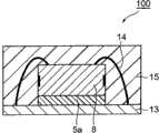
图1、2、3、及4是用于说明本发明的带粘接膜半导体芯片的制造方法的优选的一实施方式的剖面示意图。本实施方式的带粘接膜半导体芯片的制造方法具备以下工序:准备层叠体20的工序(图2),其将半导体晶片1、本发明的半导体用粘接膜5及切割带6以所述顺序层叠;通过将分割带6沿多个半导体芯片8相互分离的方向拉伸,不分割半导体用粘接膜5地将半导体晶片1分割为多个半导体芯片8的工序(图3);以及通过将多个半导体芯片8分别沿层叠体的层叠方向拾起,由此分割半导体用粘接膜5,从而得到带粘接膜半导体芯片30的工序(图4)。经过这些工序所得的带粘接膜半导体芯片30具有毛刺非常少、与半导体芯片8大致为同一形状的粘接膜5a。1 , 2 , 3 , and 4 are schematic cross-sectional views illustrating a preferred embodiment of a method for manufacturing a semiconductor chip with an adhesive film according to the present invention. The method of manufacturing a semiconductor chip with an adhesive film according to the present embodiment includes the following steps: a step of preparing a laminate 20 ( FIG. sequential lamination; by stretching the dividing
图2所示的半导体晶片1具有通过激光的照射而形成的用于将半导体晶片分割为多个半导体芯片的改性部3。对于该改性部3而言,例如可以通过对半导体晶片1与背面研磨带2的层叠体从半导体晶片1的电路面的相反侧照射激光4从而选择性地形成(图1)。该利用激光的照射的加工可利用在作为所谓隐形切割而已知的方法中通常采用的条件来实施。The semiconductor wafer 1 shown in FIG. 2 has a modified portion 3 for dividing the semiconductor wafer into a plurality of semiconductor chips formed by irradiation of laser light. The modified portion 3 can be selectively formed, for example, by irradiating the laminated body of the semiconductor wafer 1 and the back grinding tape 2 with laser light 4 from the side opposite to the circuit surface of the semiconductor wafer 1 ( FIG. 1 ). The processing by irradiation with laser light can be performed under conditions generally employed in a method known as so-called stealth dicing.
作为半导体晶片1,除了单晶硅以外,可使用由多晶硅、各种陶瓷、砷化镓等化合物半导体等构成的晶片。作为背面研磨带2,使用聚对苯二甲酸乙二醇酯系带等。As the semiconductor wafer 1 , wafers made of polycrystalline silicon, various ceramics, compound semiconductors such as gallium arsenide, etc. can be used in addition to single crystal silicon. As the back grinding tape 2, a polyethylene terephthalate tape or the like is used.
层叠体20可通过以下方法进行准备:在形成有改性部3的半导体晶片1的背面(与背面研磨带2侧相反的面)依次粘贴半导体用粘接膜5及切割带6的方法;或将层叠有半导体用粘接膜5及切割带6的复合片按照半导体用粘接膜5位于半导体晶片1侧的朝向粘贴在半导体晶片1的背面的方法。得到层叠体20的工序并不限于本实施方式这样的顺序。例如,也可以在将半导体用粘接膜粘贴在半导体晶片上后,利用激光加工形成改性部。The laminated body 20 can be prepared by the following method: a method of sticking the
切割带6只要是对固定用环具有可固定的程度的粘合性、且可沿着改性部3拉伸而分割半导体晶片的切割带,就可以没有限定地使用。例如可以将氯乙烯系带作为切割带使用。作为商业上可得到的切割带,可举出“AF-80H”、“T-80MW”(以上为日本电气化学工业社制,商品名)等。The
图2中表示了在半导体晶片1上层叠有背面研磨带2的状态,但背面研磨带2在下一个工序之前被剥离。另外,图2所示的层叠体20的切割带6上具备作为固定用环的晶片环7。FIG. 2 shows the state where the back grinding tape 2 is stacked on the semiconductor wafer 1, but the back grinding tape 2 is peeled off before the next process. In addition, the dicing
在将半导体晶片1分割为多个半导体芯片8的工序中,剥离背面研磨带后,通过将扩展环9从切割带6的下侧推到上方(图3的箭头A的方向),切割带6沿多个半导体芯片8相互分离的方向(图3的箭头B的方向)被拉伸。于是,半导体晶片1以改性部3为起点被分割为多个半导体芯片8。根据该方法,由于不必利用切割刀来切断半导体晶片1,因此,可以提高半导体晶片的单片化的速度。切割带6的扩展可以用芯片接合装置实施。In the process of dividing the semiconductor wafer 1 into a plurality of
半导体用粘接膜5在上述扩展工序中不被分割,而在下一个拾起工序中被分割。因而,切割带6的扩展量只要是可以分割半导体晶片1的范围的扩展量即可。在初始的分割带6的最大宽度为200~300mm范围的情况下,对扩展量而言,以拉伸后的切割带6的宽度(最大宽度)与初始的切割带6的宽度(最大宽度)之差计,优选为1~20mm、更优选为2~15mm、进一步优选为3~10mm。The
本实施方式的切割带6的扩展量可以比目前的通过扩展切断半导体用粘接膜的扩展量少。因此没有必要另外准备现有的隐形切割方式中使用的扩展装置。The amount of stretching of the dicing
另外,本实施方式中,拉伸切割带6的速度(扩展速度)优选为1~50mm/秒、更优选为2~30mm/秒、进一步优选为3~20mm/秒。当扩展速度小于1mm/秒时,有难以完全分割半导体晶片1的趋势。In addition, in the present embodiment, the speed (expanding speed) of stretching the dicing
在拾起多个半导体芯片的工序中,用吸附罩11真空吸附经扩展的切割带的下侧,用顶出针(Ejector pin)10顶出具有将要拾起的半导体芯片的部位,通过拾起夹12将半导体芯片8沿层叠体的层叠方向(图4的箭头符号C的方向)。此时,对半导体用粘接膜5沿其厚度方向施加剪切力,以半导体芯片8的形状将其分割。由此,可得到粘贴有毛刺非常少、与半导体芯片大致为同一形状的粘接膜5a的带粘接膜半导体芯片30。In the process of picking up a plurality of semiconductor chips, the underside of the expanded dicing tape is vacuum-adsorbed with the
作为上述工序中使用的拾起方式,优选瑞萨东日本半导体公司的多芯顶出方式、三段顶出方式等作为薄层芯片用而开发的方式。As the pick-up method used in the above-mentioned process, Renesas East Japan Semiconductor Co., Ltd.'s multi-core ejection method and three-stage ejection method are preferably developed for thin-layer chips.
在使用多芯顶出方式或通常的针顶出方式的情况下,作为针的配置,优选在芯片四角附近及其之间等间隔地配置针。特别是在多芯顶出方式的情况下,由于过多配置针时会减弱来自切割带下侧的吸附效果,因此,若为10mm×10mm左右的尺寸,则优选配置9根左右。When the multi-core ejection method or the normal needle ejection method is used, it is preferable to arrange the needles at equal intervals near and between the four corners of the chip as the arrangement of the needles. Especially in the case of the multi-core ejection method, since the adsorption effect from the lower side of the dicing tape will be weakened if too many needles are arranged, it is preferable to arrange about 9 needles if the size is about 10mm×10mm.
另外,拾起半导体芯片的拾起夹12优选制成与芯片尺寸大致相同的尺寸。作为顶出针时的条件,顶出高度优选最大值为2000μm以下、更优选为700μm以下、进一步优选为600μm以下、特别优选为500μm以下。当顶出高度超过2000μm时,芯片可能破裂,因此不优选。In addition, the pick-up
顶出针的速度优选20~200mm/s、更优选30~150mm/s、进一步优选50~100mm/s。当速度小于20mm/s时,顶出时有难以分割芯片接合膜的趋势,当超过200mm/s时,因冲击导致半导体芯片破损的可能性升高,因此不优选。The speed of ejecting the needle is preferably 20 to 200 mm/s, more preferably 30 to 150 mm/s, even more preferably 50 to 100 mm/s. When the speed is less than 20 mm/s, it tends to be difficult to split the die-bonding film during ejection, and when it exceeds 200 mm/s, the possibility of breaking the semiconductor chip due to impact increases, which is not preferable.
在本实施方式中,也可以将顶出分为2个以上的阶段进行。例如,可以在顶出高度250~1000μm、顶出速度50~100mm/s的条件下进行第1阶段;在顶出高度1000~2000μm、顶出速度1~30mm/s的条件下进行第2阶段的针的顶出。In the present embodiment, the ejection may be performed in two or more steps. For example, the first stage can be carried out under the conditions of the ejection height of 250-1000 μm and the ejection speed of 50-100 mm/s; the second stage can be carried out under the conditions of the ejection height of 1000-2000 μm and the ejection speed of 1-30 mm/s ejection of the needle.
在本实施方式中,通过应用本发明的特定的半导体用粘接膜,在上述拾起工序中可从半导体用粘接膜分割出毛刺非常少、与半导体芯片大致为同一形状的粘接膜5a。In this embodiment, by applying the specific adhesive film for semiconductors of the present invention, an
下面,对本发明的半导体用粘接膜进行说明。Next, the adhesive film for semiconductors of the present invention will be described.
本发明的半导体用粘接膜具有1~15μm范围的厚度,具有小于5%的拉伸断裂伸长率,且该拉伸断裂伸长率小于最大负荷时的伸长率的110%。这样的半导体用粘接膜含有热固性树脂及/或热塑性树脂而构成。The adhesive film for a semiconductor of the present invention has a thickness in the range of 1 to 15 μm and a tensile elongation at break of less than 5%, which is less than 110% of the elongation at maximum load. Such an adhesive film for a semiconductor contains a thermosetting resin and/or a thermoplastic resin, and is comprised.
当半导体用粘接膜的厚度小于1μm时,粘接膜的制作变难,当超过15μm时,难以通过半导体芯片的拾起分割半导体用粘接膜。另外,当半导体用粘接膜的拉伸断裂伸长率为5%以上时,需要将切割带的拉伸量增大至通常以上。另外,拉伸断裂伸长率相对于最大负荷时的伸长率的比例为110%以上的情况表示屈服状态长或容易引起缩颈(necking),这种情况下,由于难以在抑制毛刺产生的同时将半导体用粘接膜完全分割,因此,难以得到与半导体芯片的形状相吻合的粘接膜。When the thickness of the adhesive film for a semiconductor is less than 1 μm, production of the adhesive film becomes difficult, and when it exceeds 15 μm, it becomes difficult to divide the adhesive film for a semiconductor by picking up a semiconductor chip. In addition, when the tensile elongation at break of the adhesive film for semiconductors is 5% or more, it is necessary to increase the stretching amount of the dicing tape to more than normal. In addition, when the ratio of the tensile elongation at break to the elongation at the maximum load is 110% or more, it means that the yield state is long or necking is likely to occur. At the same time, since the adhesive film for semiconductors is completely divided, it is difficult to obtain an adhesive film conforming to the shape of the semiconductor chip.
从与上述相同的观点考虑,拉伸断裂伸长率优选小于4%、更优选小于3.5%。同样,拉伸断裂伸长率相对于最大负荷时的伸长率的比率优选小于108%、更优选小于105%。需要说明的是,拉伸断裂伸长率与最大负荷时的伸长率一致时,该比率为最低值的100%。From the same viewpoint as above, the tensile elongation at break is preferably less than 4%, more preferably less than 3.5%. Likewise, the ratio of tensile elongation at break to elongation at maximum load is preferably less than 108%, more preferably less than 105%. In addition, when the tensile elongation at break coincides with the elongation at the maximum load, this ratio is 100% of the minimum value.
最大应力、最大负荷伸长率及拉伸断裂伸长率使用由B阶段状态的半导体用粘接膜裁成的具有宽度5mm、长度50mm及厚度25μm的尺寸的长条状试验片,在25℃的环境下、在以下的条件下进行拉伸试验而求出。Maximum stress, maximum load elongation, and tensile elongation at break are measured at 25°C using a strip-shaped test piece cut from an adhesive film for semiconductors in a B-stage state with a width of 5 mm, a length of 50 mm, and a thickness of 25 μm. It was obtained by carrying out a tensile test under the following conditions under the environment.
拉伸试验机:SIMADZU制100N autograph“AGS-100NH”Tensile testing machine: SIMADZU 100N autograph "AGS-100NH"
夹盘间距离(试验开始时):30mmDistance between chucks (at the beginning of the test): 30mm
拉伸速度:5mm/分钟Tensile speed: 5mm/min
从由拉伸试验所得到的应力-变形曲线读取最大负荷、最大负荷时的夹盘间长度及断裂时的夹盘间的长度,使用这些值和试样断面积的实测值,利用下述式计算出最大应力、最大负荷伸长率及拉伸断裂伸长率。From the stress-deformation curve obtained by the tensile test, read the maximum load, the length between the chucks at the time of the maximum load, and the length between the chucks at the time of fracture, and use these values and the actual measurement value of the cross-sectional area of the specimen, using the following Calculate the maximum stress, maximum load elongation and tensile elongation at break.
最大应力(Pa)=最大负荷(N)/试样的断面积(m2)Maximum stress (Pa) = maximum load (N) / sectional area of the sample (m2 )
最大负荷时的伸长率(%)={(最大负荷时的夹盘间长度(mm)-30)/30}×100Elongation at maximum load (%) = {(length between chucks at maximum load (mm)-30)/30}×100
拉伸断裂伸长率(%)={(断裂时的夹盘间长度(mm)-30)/30}×100Tensile elongation at break (%)={(length between chucks at break (mm)-30)/30}×100
通常,对多个试验片进行测定,将其平均值记录为该半导体用粘接膜的拉伸特性。从重现性的观点考虑,拉伸试验优选在上述条件下进行,但也可以变更为实质上给予相同的试验结果的其它条件。Usually, several test pieces are measured, and the average value is recorded as the tensile characteristic of the adhesive film for semiconductors. From the viewpoint of reproducibility, the tensile test is preferably performed under the above-mentioned conditions, but it may be changed to other conditions that give substantially the same test results.
另外,从与被粘物的密合性及膜的分割性的观点考虑,半导体用粘接膜的厚度优选3~15μm、更优选5~15μm。In addition, the thickness of the adhesive film for a semiconductor is preferably 3 to 15 μm, more preferably 5 to 15 μm, from the viewpoint of the adhesiveness with the adherend and the separability of the film.
半导体用粘接膜5优选含有高分子量成分、热固性成分及填充剂。通过由这些成分来构成半导体用粘接膜5并调节各成分的种类及配合量,可得到具有上述特定的拉伸特性的半导体用粘接膜5。作为高分子量成分,优选热塑性树脂。The
构成半导体用粘接膜的高分子量成分优选具有60℃以下的玻璃化温度(Tg)。另外,优选具有300℃以上的耐热性的高分子量成分。作为优选的高分子量成分的具体例,可举出聚酰亚胺树脂、聚酰胺酰亚胺树脂、苯氧基树脂、丙烯酸树脂、聚酰胺树脂及聚氨酯树脂。这些高分子量成分可以使用1种或组合多种使用。其中,特别优选聚酰亚胺树脂。通过使用聚酰胺树脂,可以在将填充剂含量维持在一定程度的少量的同时,容易地赋予半导体用粘接膜5如上所述的拉伸特性。The high molecular weight component constituting the adhesive film for a semiconductor preferably has a glass transition temperature (Tg) of 60°C or lower. In addition, a high molecular weight component having heat resistance of 300° C. or higher is preferable. Specific examples of preferable high molecular weight components include polyimide resins, polyamideimide resins, phenoxy resins, acrylic resins, polyamide resins, and polyurethane resins. These high molecular weight components may be used alone or in combination. Among them, polyimide resins are particularly preferable. By using a polyamide resin, the above-mentioned tensile properties can be easily imparted to the
热固性成分是能够通过加热交联而形成固化体的成分,例如,可由热固性树脂及其固化剂构成。作为热固性树脂,可以使用目前公知的树脂,没有特别限定,其中,从作为半导体周边材料的便利性(容易得到高纯度制品、品种多、容易控制反应性)方面考虑,优选环氧树脂及1个分子中至少具有2个热固性酰亚胺基的酰亚胺化合物。环氧树脂通常与环氧树脂固化剂并用。The thermosetting component is a component capable of crosslinking by heating to form a cured body, and may be composed of, for example, a thermosetting resin and its curing agent. As the thermosetting resin, conventionally known resins can be used without any particular limitation. Among them, epoxy resins and a An imide compound having at least two thermosetting imide groups in the molecule. Epoxy resins are often used in combination with epoxy resin curing agents.
环氧树脂优选为具有2个以上环氧基的化合物。从固化性或固化物特性方面考虑,优选酚的缩水甘油醚型的环氧树脂。作为酚的缩水甘油醚型的环氧树脂,可举出例如:双酚A、双酚AD、双酚S、双酚F或卤化双酚A与表氯醇的缩合物、苯酚酚醛清漆树脂的缩水甘油醚、甲酚酚醛清漆树脂的缩水甘油醚、及双酚A酚醛清漆树脂的缩水甘油醚。其中,尤其是从固化物的交联密度高、可以使膜的热时的粘接强度升高方面考虑,优选酚醛清漆型环氧树脂(甲酚酚醛清漆树脂的缩水甘油醚及苯酚酚醛清漆树脂的缩水甘油醚等)。这些树脂可以单独使用或组合二种以上使用。The epoxy resin is preferably a compound having two or more epoxy groups. From the viewpoint of curability and cured product properties, a glycidyl ether type epoxy resin of phenol is preferable. Examples of glycidyl ether-type epoxy resins of phenol include bisphenol A, bisphenol AD, bisphenol S, bisphenol F, or condensates of halogenated bisphenol A and epichlorohydrin, and phenol novolac resins. Glycidyl ether, glycidyl ether of cresol novolac resin, and glycidyl ether of bisphenol A novolak resin. Among them, especially from the viewpoint that the crosslinking density of the cured product is high and the bonding strength during heat of the film can be increased, novolac type epoxy resins (glycidyl ether of cresol novolak resin and phenol novolak resin) are preferred. glycidyl ether, etc.). These resins can be used alone or in combination of two or more.
作为环氧树脂固化剂,可举出例如:酚系化合物、脂肪族胺、脂环族胺、芳香族多胺、聚酰胺、脂肪族酸酐、脂环族酸酐、芳香族酸酐、双氰胺、有机酸二酰肼、三氟化硼胺络合物、咪唑类及叔胺。其中,尤其优选酚系化合物,酚系化合物中,特别优选具有2个以上酚性羟基的酚系化合物。更具体而言,优选萘酚酚醛清漆树脂及三苯酚酚醛清漆树脂。当使用这些酚系化合物作为环氧树脂固化剂时,可以有效地减少用于封装组装的加热时的芯片表面及装置的污染及成为臭味的原因的脱气(out gas)的发生。Examples of epoxy resin curing agents include phenolic compounds, aliphatic amines, alicyclic amines, aromatic polyamines, polyamides, aliphatic acid anhydrides, alicyclic acid anhydrides, aromatic acid anhydrides, dicyandiamide, Organic acid dihydrazides, boron trifluoride amine complexes, imidazoles and tertiary amines. Among them, phenolic compounds are particularly preferred, and among the phenolic compounds, phenolic compounds having two or more phenolic hydroxyl groups are particularly preferred. More specifically, naphthol novolak resins and trisphenol novolac resins are preferred. When these phenolic compounds are used as epoxy resin curing agents, it is possible to effectively reduce the contamination of chip surfaces and devices and the occurrence of outgassing (out gas), which is a cause of odor, during heating for package assembly.
通过调节填充剂的含量,可以控制半导体用粘接膜的拉伸特性。当填充剂的含量增多时,有拉伸断裂伸长率变小的趋势及拉伸断裂伸长率相对于最大负荷时的伸长率的比率减小的趋势。另外,通过使用适量填充剂,还可得到改善操作性、改善导热性、调节熔融粘度、赋予触变性等效果。By adjusting the content of the filler, the tensile properties of the adhesive film for semiconductors can be controlled. When the content of the filler increases, the tensile elongation at break tends to decrease and the ratio of the tensile elongation at break to the elongation at maximum load tends to decrease. In addition, by using an appropriate amount of filler, effects such as improvement of workability, improvement of thermal conductivity, adjustment of melt viscosity, and imparting of thixotropy can be obtained.
从上述目的的观点考虑,填充剂优选为无机填充剂。更具体而言,优选含有选自氢氧化铝、氢氧化镁、碳酸钙、碳酸镁、硅酸钙、硅酸镁、氧化钙、氧化镁、氧化铝、氮化铝、硼酸铝晶须、氮化硼、结晶二氧化硅、非结晶二氧化硅及锑氧化物中的至少1种无机材料的无机填充剂。这些无机物中,为了提高导热性,尤其优选氧化铝、氮化铝、氮化硼、结晶二氧化硅及非结晶二氧化硅。为了调节熔融粘度及赋予触变性,优选氢氧化铝、氢氧化镁、碳酸钙、碳酸镁、硅酸钙、硅酸镁、氧化钙、氧化镁、氧化铝、结晶二氧化硅及非结晶二氧化硅。另外,为了改善耐湿性,优选氧化铝、二氧化硅、氢氧化铝及锑氧化物。也可以将多种填充剂混合使用。From the viewpoint of the above purpose, the filler is preferably an inorganic filler. More specifically, it preferably contains a compound selected from the group consisting of aluminum hydroxide, magnesium hydroxide, calcium carbonate, magnesium carbonate, calcium silicate, magnesium silicate, calcium oxide, magnesium oxide, aluminum oxide, aluminum nitride, aluminum borate whiskers, nitrogen An inorganic filler of at least one inorganic material selected from boron oxide, crystalline silica, amorphous silica, and antimony oxide. Among these inorganic substances, aluminum oxide, aluminum nitride, boron nitride, crystalline silica, and amorphous silica are particularly preferable in order to improve thermal conductivity. In order to adjust melt viscosity and impart thixotropy, aluminum hydroxide, magnesium hydroxide, calcium carbonate, magnesium carbonate, calcium silicate, magnesium silicate, calcium oxide, magnesium oxide, aluminum oxide, crystalline silica and amorphous silica are preferred. silicon. In addition, in order to improve moisture resistance, alumina, silica, aluminum hydroxide, and antimony oxide are preferable. Multiple types of fillers can also be used in combination.
当填充剂的含量变多时,在拉伸断裂伸长率变小的同时弹性模量变高而有断裂强度上升的趋势,另一方面,因粘接性下降而有耐软熔裂纹(reflow crack)性下降的趋势。特别是在有机基板之类的表面形成有凹凸的被粘物和半导体芯片之间软熔时有容易促进破坏的趋势。另外,当填充剂变多时,还有在HAST试验等高温高湿环境下的对可靠性试验的耐受性下降的趋势。进而,当填充剂的含量变多时,可将半导体用粘接膜粘贴到半导体晶片上的温度也存在上升的趋势。鉴于如上所述的情况,填充剂的含量相对于半导体用粘接膜的全部质量优选为小于30质量%、更优选为小于25质量%、进一步优选为小于20质量%。When the content of the filler increases, the elastic modulus tends to increase while the tensile elongation at break decreases, and the breaking strength tends to increase. On the other hand, due to the decrease in adhesion, reflow crack resistance ) a downward trend. In particular, when reflow occurs between an adherend having unevenness formed on the surface such as an organic substrate and a semiconductor chip, destruction tends to be accelerated. In addition, when the filler increases, the resistance to reliability tests in high-temperature, high-humidity environments such as HAST tests tends to decrease. Furthermore, when the content of the filler increases, the temperature at which the adhesive film for a semiconductor can be bonded to the semiconductor wafer also tends to increase. In view of the above, the content of the filler is preferably less than 30% by mass, more preferably less than 25% by mass, and still more preferably less than 20% by mass, based on the entire mass of the adhesive film for semiconductors.
半导体用粘接膜5优选在100℃以下的温度可粘贴在作为被粘物的半导体晶片上。在此,在半导体晶片上粘贴保持在规定温度的半导体用粘接膜时,只要半导体用粘接膜和半导体晶片的界面的剥离强度为20N/m以上,就可判断为能够粘贴在半导体晶片上。半导体用粘接膜例如可使用设定在100℃以下的温度的热辊压膜机(Hot Roll Laminator)粘贴在半导体晶片上。剥离强度的测定在25℃的环境中、拉伸角度90°、拉伸速度50mm/分钟下进行。例如,通过减少填充剂的含量、或使用具有低Tg的热塑性树脂,可得到在100℃以下可粘贴在半导体晶片上的半导体用粘接膜。半导体用粘接膜5可粘贴在半导体晶片上的温度更优选为95℃以下、进一步优选为90℃以下。在考虑背面研磨带的耐热性的情况下,半导体用粘接膜5优选在80℃以下的温度能够粘贴在作为被粘物的半导体晶片上。It is preferable that the
半导体用粘接膜5优选具有在将半导体芯片搭载在半导体芯片搭载用支撑部件上时所要求的耐热性及耐湿性。因此,优选其通过耐软熔裂纹性试验。可以以粘接强度为指标来评价半导体用粘接膜的耐软熔裂纹性。为了得到良好的耐软熔裂纹性,在半导体晶片上以4×2mm见方的粘接面积粘接半导体用粘接膜时,优选在剥离强度初始为1.0kg/cm以上、85℃/85%的环境下放置48小时后为0.5kg/cm以上。初始的剥离强度更优选为1.3kg/cm以上、进一步优选为1.5kg/cm。在85℃/85%的环境下放置48小时后的剥离强度更优选为0.7kg/cm以上、进一步优选为0.8kg/cm以上。It is preferable that the
半导体用粘接膜5例如可以用将含有热塑性树脂等高分子量成分、热固性成分、填充剂及溶解或分散这些物质的有机溶剂的涂敷液涂敷在基材膜上并通过加热从基材膜上的涂敷液中除去有机溶剂的方法来得到。The
有机溶剂只要是能够将材料均匀地溶解或分散的溶剂就没有限定,可举出例如:二甲基甲酰胺、二甲基乙酰胺、N-甲基吡咯烷酮、二甲基亚砜、二甘醇二甲醚、甲苯、苯、二甲苯、甲基乙基酮、四氢呋喃、乙基溶纤剂、乙基溶纤剂醋酸酯、丁基溶纤剂、二噁烷、环己酮及醋酸乙酯。这些溶剂可以单独或组合二种以上使用。The organic solvent is not limited as long as it can dissolve or disperse the material uniformly, for example: dimethylformamide, dimethylacetamide, N-methylpyrrolidone, dimethylsulfoxide, diethylene glycol Dimethyl ether, toluene, benzene, xylene, methyl ethyl ketone, tetrahydrofuran, ethyl cellosolve, ethyl cellosolve acetate, butyl cellosolve, dioxane, cyclohexanone, and ethyl acetate. These solvents can be used alone or in combination of two or more.
基材膜只要是可以耐受用于除去有机溶剂而进行的加热的材料就没有特别限定。作为基材膜的例子,可举出:聚酯膜、聚丙烯膜、聚对苯二甲酸乙二醇酯膜、聚酰亚胺膜、聚醚酰亚胺膜、聚醚萘酸酯及甲基戊烯膜。也可以将组合有2种以上这些膜的多层膜用作基材膜。基材膜的表面也可以用硅酮系、二氧化硅系等脱模剂等进行处理。除去有机溶剂后,也可以不除去基材膜,而直接用作半导体用粘接膜的支撑体。The base film is not particularly limited as long as it is a material that can withstand heating for removing the organic solvent. Examples of the base film include: polyester film, polypropylene film, polyethylene terephthalate film, polyimide film, polyetherimide film, polyether naphthalate, and formaldehyde pentene film. A multilayer film in which two or more of these films are combined can also be used as the base film. The surface of the base film may be treated with a silicone-based, silica-based, or other release agent. After removing the organic solvent, it can also be used as a support body of the adhesive film for semiconductors without removing the base film.
半导体用粘接膜还可以以与切割带粘贴在一起的复合片的状态保管及使用。通过使用这样的复合片,可以简化半导体装置制造工序。The adhesive film for semiconductors can also be stored and used in the state of a composite sheet bonded to a dicing tape. By using such a composite sheet, the semiconductor device manufacturing process can be simplified.
本发明的带粘接膜半导体芯片的制造方法中使用的半导体用粘接膜也可以是以具有下述构成的芯片接合膜的形式供给的膜。The adhesive film for semiconductors used in the method of manufacturing a semiconductor chip with an adhesive film of the present invention may be supplied as a die-bonding film having the following configuration.
(a)依次具备基材和含有热固性树脂及/或热塑性树脂的粘接剂层的芯片接合膜。(a) A die-bonding film provided with a substrate and an adhesive layer containing a thermosetting resin and/or a thermoplastic resin in this order.
(b)依次具备基材、粘合剂层和含有热固性树脂及/或热塑性树脂的粘接剂层的芯片接合膜。(b) A die-bonding film provided with a base material, an adhesive layer, and an adhesive layer containing a thermosetting resin and/or a thermoplastic resin in this order.
(c)依次具备基材和含有热固性树脂及/或热塑性树脂的粘合/粘接剂层的芯片接合膜。(c) A die-bonding film provided with a substrate and an adhesion/adhesive layer containing a thermosetting resin and/or a thermoplastic resin in this order.
(a)及(b)的芯片接合膜中的粘接剂层以及(c)的芯片接合膜中的粘合·粘接剂层是上述的本发明的半导体用粘接膜。The adhesive layer in the die-bonding film of (a) and (b) and the adhesive agent layer in the die-bonding film of (c) are the adhesive film for semiconductors of this invention mentioned above.
在使用(a)的芯片接合膜的情况下,可以利用以下的任一方法得到本发明的层叠体。When using the die-bonding film of (a), the laminated body of this invention can be obtained by any of the following methods.
(1)首先,将上述(a)的芯片接合膜的粘接剂层和半导体晶片贴合在一起。其次,将芯片接合膜的基材剥离。其次,将依次具备粘合剂层和基材的切割带部件的粘合剂层与粘接剂层贴合在一起。(1) First, the adhesive layer of the die-bonding film of the above (a) and the semiconductor wafer are bonded together. Next, the base material of the die-bonding film is peeled off. Next, the pressure-sensitive adhesive layer and the pressure-sensitive adhesive layer of the dicing tape member provided with the pressure-sensitive adhesive layer and the base material in this order are bonded together.
(2)首先,将上述(a)的芯片接合膜的粘接剂层与依次具备粘合剂层和基材层的切割带部件的粘合剂层贴合在一起。其次,将芯片接合膜的基材剥离,将粘接剂层和半导体晶片贴合在一起。(2) First, the adhesive layer of the die-bonding film of the above (a) and the adhesive layer of the dicing tape member provided with the adhesive layer and the base material layer in this order are bonded together. Next, the base material of the die-bonding film is peeled off, and the adhesive layer and the semiconductor wafer are bonded together.
在使用(b)的芯片接合膜的情况下,可以利用以下的方法得到本发明的层叠体。When using the die-bonding film of (b), the laminated body of this invention can be obtained by the following method.
(3)将上述(b)的芯片接合膜的粘接剂层和半导体晶片贴合在一起。在基材及粘合剂层作为切割带发挥作用时,由此可以得到层叠体。需要说明的是,也可以在将基材剥离后将切割带贴合在粘合剂层上而得到层叠体。(3) The adhesive layer of the die-bonding film of said (b) and a semiconductor wafer are bonded together. When the base material and the pressure-sensitive adhesive layer function as a dicing tape, a laminated body can be obtained thereby. In addition, after peeling a base material, you may bond a dicing tape to an adhesive layer, and obtain a laminated body.
在使用(c)的芯片接合膜的情况下,可以利用以下的方法得到本发明的层叠体。When using the die-bonding film of (c), the laminated body of this invention can be obtained by the following method.
(4)首先,将上述(c)的芯片接合膜的粘合/粘接剂层和半导体晶片贴合在一起。在基材作为切割带发挥作用时,可以由此得到层叠体。需要说明的是,也可以在将基材剥离后将切割带贴合在粘合剂层上而得到层叠体。(4) First, the adhesion/adhesive layer of the die-bonding film of the above (c) and the semiconductor wafer are bonded together. When the base material functions as a dicing tape, a laminated body can be obtained thereby. In addition, after peeling a base material, you may bond a dicing tape to an adhesive layer, and obtain a laminated body.
如使用上述(c)的芯片接合膜的例子所示,本发明还可以提供带粘接膜半导体芯片的制造方法,该制造方法具备以下工序:准备层叠体的工序,将半导体晶片、膜状粘合/粘接剂及基材以所述顺序层叠,上述膜状粘合/粘接剂具有1~15μm范围的厚度、具有小于5%的拉伸断裂伸长率、且该拉伸断裂伸长率小于最大负荷时的伸长率的110%,上述半导体晶片具有由激光照射而形成的用于将半导体晶片分割为多个半导体芯片的改性部;将上述基材沿多个半导体芯片相互分离的方向拉伸,从而不分割上述膜状粘合/粘接剂地将半导体晶片分割为多个半导体芯片的工序;以及,将多个半导体芯片分别沿层叠体的层叠方向拾起,从而分割上述膜状粘合/粘接剂,得到带粘接膜半导体芯片的工序。上述基材可以使用作为切割带发挥作用的基材。As shown in the example of using the die-bonding film of the above (c), the present invention can also provide a method of manufacturing a semiconductor chip with an adhesive film, which includes the following steps: a step of preparing a laminate, bonding the semiconductor wafer, film-shaped adhesive The bonding/adhesive and the substrate are laminated in the order described above, and the above-mentioned film-like adhesive/adhesive has a thickness in the range of 1 to 15 μm, has a tensile elongation at break of less than 5%, and the tensile elongation at break is The ratio is less than 110% of the elongation at the time of the maximum load, and the above-mentioned semiconductor wafer has a modified portion for dividing the semiconductor wafer into a plurality of semiconductor chips formed by laser irradiation; the above-mentioned base material is separated from each other along the plurality of semiconductor chips The process of stretching in the direction of the above-mentioned film-like adhesive/adhesive to divide the semiconductor wafer into a plurality of semiconductor chips; Film-like adhesive/adhesive, the process of obtaining a semiconductor chip with an adhesive film. As the above-mentioned base material, a base material functioning as a dicing tape can be used.
在本实施方式中,说明了将本发明的半导体用粘接膜配置在半导体晶片背面侧的情况,但本发明的带粘接膜半导体芯片的制造方法也可以在将半导体晶片的电路面和半导体用粘接膜粘贴在一起的方式中使用。In this embodiment mode, the case where the adhesive film for a semiconductor of the present invention is disposed on the back side of the semiconductor wafer is described, but the method of manufacturing a semiconductor chip with an adhesive film of the present invention may also be placed on the circuit surface of the semiconductor wafer and the semiconductor chip. Use it by sticking it together with an adhesive film.
如上所述的利用本实施方式的方法得到的带粘接膜半导体芯片30构成例如IC、LSI之类的半导体元件。带粘接膜半导体芯片30例如可借助粘接膜5a粘接在其它的半导体芯片或半导体芯片搭载用支撑部件上。The
作为半导体芯片搭载用支撑部件,可举出例如:42合金引线框架及铜引线框架等引线框架;由环氧树脂、聚酰亚胺系树脂及马来酰亚胺系树脂等形成的树脂膜;在玻璃非织造布或玻璃织造布中浸渍环氧树脂、聚酰亚胺系树脂及马来酰亚胺系树脂等热固性树脂并使其固化所得的基板;以及玻璃基板及氧化铝等陶瓷基板。Examples of supporting members for mounting semiconductor chips include lead frames such as 42 alloy lead frames and copper lead frames; resin films made of epoxy resin, polyimide-based resin, and maleimide-based resin; Substrates obtained by impregnating thermosetting resins such as epoxy resins, polyimide-based resins, and maleimide-based resins in glass nonwoven fabrics or glass woven fabrics and curing them; and glass substrates and ceramic substrates such as alumina.
图5是表示由该方法得到的半导体装置的一实施方式的剖面图。图5所示的半导体装置100具备带配线基材(支撑部件)13和借助粘接膜5a粘接在带配线基材13上的半导体芯片8。半导体芯片8通过接合线14与带配线基材13的配线连接。另外,半导体芯片8利用埋设这些部件的密封树脂层15进行密封。FIG. 5 is a cross-sectional view showing an embodiment of a semiconductor device obtained by this method. The
对于半导体芯片和支撑部件的粘接及半导体芯片之间的粘接,例如可以在将半导体用粘接膜夹持在半导体芯片和支撑部件之间或半导体芯片彼此之间的状态下以60~300℃加热0.1~300秒来进行。For the bonding of the semiconductor chip and the supporting member and the bonding between the semiconductor chips, for example, the adhesive film for the semiconductor can be sandwiched between the semiconductor chip and the supporting member or between the semiconductor chips at 60 to 300°C. Heating is performed for 0.1 to 300 seconds.
半导体用粘接膜5含有热固性树脂时,优选加热粘接后的半导体芯片来促进半导体用粘接膜在被粘物上的密合或固化,从而增加接合部的强度。此时的加热根据粘接膜的组成适当调节即可,通常为60~220℃、0.1~600分钟。进行树脂密封时,也可以利用密封树脂的固化工序的加热。When the
实施例Example
下面,利用实施例详细地说明本发明。但是,本发明并不限定于这些实施例。Next, the present invention will be described in detail using examples. However, the present invention is not limited to these Examples.
<半导体用粘接膜的制作><Production of Adhesive Films for Semiconductors>
(实施例1)(Example 1)
在具备温度计、搅拌器及氯化钙管的500ml四口烧瓶中放入作为二胺化合物的1,3-双(3-氨基丙基)四甲基二硅氧烷(0.06mol)、4,9-二氧杂癸烷-1,12-二胺(4,9-dioxadecane-1,12-diamine)(0.04mol)及作为溶剂的N-甲基-2-吡咯烷酮150g,在60℃下进行搅拌、溶解。In a 500ml four-necked flask equipped with a thermometer, a stirrer and a calcium chloride tube, put 1,3-bis(3-aminopropyl)tetramethyldisiloxane (0.06mol), 4 as a diamine compound, 9-dioxadecane-1,12-diamine (4,9-dioxadecane-1,12-diamine) (0.04mol) and 150 g of N-methyl-2-pyrrolidone as a solvent were carried out at 60°C Stir and dissolve.
二胺化合物溶解后,分多次少量地添加1,10-(十亚甲基)双(偏苯三酸二酐)(0.02mol)和4,4’-氧双邻苯二甲酸酐(0.08mol),在60℃下使之反应3小时。其后,一边吹入N2气一边以170℃进行加热,通过共沸,用3小时将体系内的水与部分溶剂一同除去。由此,得到聚酰亚胺树脂的溶液。After the diamine compound is dissolved, add 1,10-(decamethylene)bis(trimellitic dianhydride) (0.02mol) and 4,4'-oxybisphthalic anhydride (0.08 mol) was reacted at 60°C for 3 hours. Thereafter, heating was performed at 170° C. while blowing N2 gas, and water in the system was removed together with a part of the solvent by azeotroping over 3 hours. Thus, a solution of polyimide resin was obtained.
在上述得到的聚酰亚胺树脂的NMP溶液(含聚酰亚胺树脂100质量份)中加入甲酚酚醛清漆型环氧树脂(东都化成制)4质量份、4,4’-[1-[4-[1-(4-羟基苯基)-1-甲基乙基]苯基]亚乙基]双酚(本州化学制)2质量份、四苯基鏻四苯基硼酸酯(东京化成制)0.5质量份。进而,加入相对于全部固体成分的重量为12质量%的氮化硼填充剂(水岛合金铁制)、相对于全部固体成分的重量为3质量%的AEROSIL填充剂R972(日本AEROSIL制),充分混炼,得到清漆。In the NMP solution (containing 100 parts by mass of polyimide resin) of the polyimide resin obtained above, add 4 parts by mass of cresol novolac type epoxy resin (made by Dongdu Chemical Industry), 4,4'-[1 -[4-[1-(4-Hydroxyphenyl)-1-methylethyl]phenyl]ethylene]bisphenol (manufactured by Honshu Chemical) 2 parts by mass, tetraphenylphosphonium tetraphenyl borate (Tokyo Chemical Co., Ltd.) 0.5 parts by mass. Furthermore, 12% by mass of boron nitride filler (manufactured by Mizushima Alloy Iron) relative to the weight of the total solid content and 3% by mass of AEROSIL filler R972 (manufactured by AEROSIL Japan) relative to the weight of the total solid content were added, Fully kneaded to obtain a varnish.
将调制成的清漆涂敷在剥离处理完毕的聚对苯二甲酸乙二醇酯膜(帝人杜邦公司制、膜A31、厚度50μm)上,以80℃加热30分钟,接着以120℃加热30分钟,形成厚度5μm的半导体用粘接膜。The prepared varnish was coated on a peeled polyethylene terephthalate film (manufactured by Teijin DuPont Co., Ltd., film A31, thickness 50 μm), heated at 80°C for 30 minutes, and then heated at 120°C for 30 minutes , and an adhesive film for a semiconductor with a thickness of 5 μm was formed.
(实施例2)(Example 2)
将与实施例1同样操作得到的清漆涂敷在剥离处理完毕的聚对苯二甲酸乙二醇酯膜(帝人杜邦公司制、膜A31、厚度50μm)上,以80℃加热30分钟,接着以120℃加热30分钟,形成厚度15μm的半导体用粘接膜。The varnish obtained in the same manner as in Example 1 was coated on a peeled polyethylene terephthalate film (manufactured by Teijin DuPont Co., Ltd., film A31, thickness 50 μm), heated at 80° C. for 30 minutes, and then It was heated at 120° C. for 30 minutes to form an adhesive film for semiconductors with a thickness of 15 μm.
(比较例1)(comparative example 1)
将与实施例1同样操作得到的清漆涂敷在剥离处理完毕的聚对苯二甲酸乙二醇酯膜(帝人杜邦公司制、膜A31、厚度50μm)上,以80℃加热30分钟,接着以120℃加热30分钟,形成厚度25μm的半导体用粘接膜。The varnish obtained in the same manner as in Example 1 was coated on a peeled polyethylene terephthalate film (manufactured by Teijin DuPont Co., Ltd., film A31, thickness 50 μm), heated at 80° C. for 30 minutes, and then It was heated at 120° C. for 30 minutes to form an adhesive film for semiconductors with a thickness of 25 μm.
(比较例2)(comparative example 2)
准备DF-402(日立化成工业社株式会社制、商品名、厚度15μm)作为比较例2的半导体用粘接膜。As the adhesive film for semiconductors of Comparative Example 2, DF-402 (manufactured by Hitachi Chemical Industries, Ltd., trade name,
<粘接膜的评价><Evaluation of Adhesive Film>
(最大应力、最大负荷伸长率及拉伸断裂伸长率)(maximum stress, maximum load elongation and tensile elongation at break)
使用由B阶段状态的粘接膜裁成的长条状试验片(宽度5mm、长度50mm)进行拉伸试验。由所得的应力-变形曲线基于下述算式求出最大应力、最大负荷伸长率及拉伸断裂伸长率。拉伸试验使用拉伸试验机(SIMADZU制100Nautograph、AGS-100NH),在25℃的环境中,在试验开始的夹盘间距离30mm、拉伸速度5mm/min的条件下进行。A tensile test was performed using a strip-shaped test piece (
最大应力(Pa)=最大负荷(N)/试样的断面积(m2)Maximum stress (Pa) = maximum load (N) / sectional area of the sample (m2 )
最大负荷伸长率(%)=[(最大负荷下的夹盘间长度(mm)-30)/30]×100Maximum load elongation (%)=[(length between chucks under maximum load (mm)-30)/30]×100
拉伸断裂伸长率(%)=[(断裂时的夹盘间长度(mm)-30)/30]×100Tensile elongation at break (%)=[(length between chucks at break (mm)-30)/30]×100
<带粘接膜半导体芯片的制作><Production of Semiconductor Chip with Adhesive Film>
准备通过激光照射而在内部形成有改性部的50μm厚的半导体晶片(材质:单晶硅)和背面研磨带的层叠品。需要说明的是,改性部按照能够将半导体晶片分割为10mm×10mm的大小的方式形成。A laminate of a semiconductor wafer (material: single crystal silicon) having a thickness of 50 μm in which a modified portion was formed by laser irradiation and a back grinding tape was prepared. In addition, the modified part was formed so that the semiconductor wafer could be divided into the size of 10 mm x 10 mm.
另一方面,将实施例及比较例制得的半导体用粘接膜分别裁剪为直径210mm的圆形,将所得的各半导体用粘接膜使用晶片贴片机(WaferMounter)“DM-300H”(JCM公司制、商品名),在室温、线压5kgf、10mm/s的条件下粘贴在切割带(电气化学工业社制、商品名“AD-80H”、厚度80μm)上,制作半导体用粘接膜和切割带的层叠品。需要说明的是,在该层叠品的切割带上也粘贴晶片环。On the other hand, the adhesive films for semiconductors obtained in Examples and Comparative Examples were cut into circles with a diameter of 210 mm, and each of the obtained adhesive films for semiconductors was cut using a wafer mounter (WaferMounter) "DM-300H" ( Made by JCM Co., Ltd., brand name), and pasted on a dicing tape (manufactured by Denki Kagaku Kogyo Co., Ltd., brand name "AD-80H", thickness 80μm) at room temperature, a linear pressure of 5kgf, and 10mm/s to make an adhesive for semiconductors Laminate of film and dicing tape. In addition, the wafer ring was also stuck on the dicing tape of this laminated product.
在上述准备的形成有改性部的半导体晶片的背面,使用晶片贴片机“DM-300H”(JCM公司制、商品名)在热板温度80℃、线压5kgf、3mm/s的条件下,粘贴上述半导体用粘接膜和切割带的层叠品,得到层叠体样品。需要说明的是,在粘贴前剥离背面研磨带。On the back surface of the semiconductor wafer on which the reformed part was formed prepared above, use a die mounter "DM-300H" (manufactured by JCM, trade name) under the conditions of a hot plate temperature of 80°C, a linear pressure of 5kgf, and 3mm/s. , a laminate of the above-mentioned adhesive film for a semiconductor and a dicing tape was attached to obtain a laminate sample. It should be noted that the back grinding tape should be peeled off before pasting.
接着,将上述得到的层叠体样品设置在Flexible die bonder“DB-730”(瑞萨东日本半导体公司制、商品名)上,利用扩展装置拉伸切割带。扩展速度为10mm/s,扩展量为4mm。接着,对进行扩展了的层叠体样品,利用以4.2mm间隔将9根顶出针(Micromechanics公司制、SEN-83-05:针直径0.7mm、尖端直径350μm半圆形)配置成格子状的Flexible die bonder“DB-730”(瑞萨东日本半导体公司制)的多芯顶出夹具,一边顶出针,一边使用作为拾起夹的橡胶吸嘴(rubber tip)(Micromechanics公司制、商品名:13-087E-33、10mm×10mm)拾起半导体芯片。此时,针的顶出设定为2个阶段动作,第1阶段在高度300μm、速度89.4mm/s的条件下顶出,其后,第2阶段在高度1500μm、速度8.94mm/s的条件下顶出,顶出后在保持时间(拾起时间)500ms的条件下顶出针,同时拾起半导体芯片。将此时的拾起性根据下述标准进行评价。Next, the laminated body sample obtained above was set on a flexible die bonder "DB-730" (manufactured by Renesas East Japan Semiconductor Co., Ltd., trade name), and the dicing tape was stretched by an expanding device. The expansion speed is 10mm/s, and the expansion amount is 4mm. Next, for the expanded laminate sample, nine ejection needles (manufactured by Micromechanics, SEN-83-05: needle diameter 0.7 mm, tip diameter 350 μm semicircle) were arranged in a grid pattern at intervals of 4.2 mm. Flexible die bonder "DB-730" (manufactured by Renesas East Japan Semiconductor Co., Ltd.) is a multi-core ejection jig that uses a rubber tip (manufactured by Micromechanics, trade name) as a pick-up clip while ejecting the needle. : 13-087E-33, 10mm×10mm) to pick up semiconductor chips. At this time, the ejection of the needle is set to operate in two stages. In the first stage, it is ejected under the conditions of a height of 300 μm and a speed of 89.4 mm/s. After that, in the second stage, it is ejected under the conditions of a height of 1500 μm and a speed of 8.94 mm/s. After ejection, the needle is ejected under the condition of holding time (pick-up time) of 500 ms after ejection, and the semiconductor chip is picked up at the same time. The pick-up property at this time was evaluated according to the following criteria.
[拾起性][pick up sex]
A:半导体用粘接膜被切断,能够拾起带粘接膜半导体芯片。A: The adhesive film for semiconductors was cut, and a semiconductor chip with an adhesive film could be picked up.
B:半导体用粘接膜未被完全切断,不能拾起半导体芯片,产生芯片破裂。B: The adhesive film for semiconductors was not completely cut, the semiconductor chip could not be picked up, and chip cracks occurred.
[表1][Table 1]
如表1所示,可确认利用具有1~15μm范围的厚度、具有小于5%的拉伸断裂伸长率、且该拉伸断裂伸长率小于最大负荷时的伸长率的110%的实施例1及2的半导体用粘接膜,可通过上述拾起工序分割半导体用粘接膜,得到带粘接膜半导体芯片。另外,可确认分割得到的粘接膜的毛刺非常少、且具有与半导体芯片大致相同的形状。相对于此,使用比较例1及2的半导体用粘接膜时,不能通过上述扩展工序及拾起工序分割半导体用粘接膜。As shown in Table 1, it can be confirmed that the implementation using a thickness in the range of 1 to 15 μm, having a tensile elongation at break of less than 5%, and the tensile elongation at break is less than 110% of the elongation at the maximum load The adhesive films for semiconductors of Examples 1 and 2 can be divided into semiconductor chips with adhesive films by dividing the adhesive films for semiconductors in the above-mentioned pick-up step. In addition, it was confirmed that the divided adhesive film had very few burrs and had substantially the same shape as the semiconductor chip. On the other hand, when the adhesive films for semiconductors of Comparative Examples 1 and 2 were used, the adhesive films for semiconductors could not be divided by the above-mentioned spreading step and pick-up step.
由以上的结果可知,利用使用本发明的半导体用粘接膜的带粘接膜半导体芯片的制造方法,可以得到粘贴有毛刺非常少、与半导体芯片大致为同一形状的粘接膜的带粘接膜半导体芯片,可以兼顾利用隐形切割方式的半导体装置的制造中的组装性和可靠性。From the above results, it can be seen that by using the method of manufacturing a semiconductor chip with an adhesive film using the adhesive film for semiconductors of the present invention, it is possible to obtain an adhesive tape with an adhesive film with very few burrs and substantially the same shape as the semiconductor chip. The film semiconductor chip can achieve both assembly and reliability in the manufacture of a semiconductor device using a stealth dicing method.
产业上的可利用性Industrial availability
根据本发明,可以提供在由半导体晶片高成品率地得到半导体芯片的同时,可以得到粘贴有毛刺非常少、与半导体芯片大致为同一形状的粘接膜的带粘接膜半导体芯片的带粘接膜半导体芯片的制造方法及优选用于该带粘接膜半导体芯片的制造方法的半导体用粘接膜,以及可兼顾组装性和可靠性的半导体装置的制造方法。According to the present invention, it is possible to provide a tape bonding of a semiconductor chip with an adhesive film that can obtain a semiconductor chip with a high yield rate from a semiconductor wafer and an adhesive film with very few burrs and substantially the same shape as the semiconductor chip. A method of manufacturing a film semiconductor chip, an adhesive film for a semiconductor preferably used in the method of manufacturing a semiconductor chip with an adhesive film, and a method of manufacturing a semiconductor device capable of both assembly and reliability.
Claims (3)
Applications Claiming Priority (3)
| Application Number | Priority Date | Filing Date | Title |
|---|---|---|---|
| JP2007263346 | 2007-10-09 | ||
| JP2007-263346 | 2007-10-09 | ||
| PCT/JP2008/068236WO2009048060A1 (en) | 2007-10-09 | 2008-10-07 | Method for producing semiconductor chip with adhesive film, adhesive film for semiconductor used in the method, and method for producing semiconductor device |
Related Child Applications (1)
| Application Number | Title | Priority Date | Filing Date |
|---|---|---|---|
| CN201110314139XADivisionCN102361016A (en) | 2007-10-09 | 2008-10-07 | Adhesive film for semiconductor, semiconductor chip, and method for processing semiconductor device |
Publications (2)
| Publication Number | Publication Date |
|---|---|
| CN101821833Atrue CN101821833A (en) | 2010-09-01 |
| CN101821833B CN101821833B (en) | 2012-04-04 |
Family
ID=40549204
Family Applications (2)
| Application Number | Title | Priority Date | Filing Date |
|---|---|---|---|
| CN201110314139XAPendingCN102361016A (en) | 2007-10-09 | 2008-10-07 | Adhesive film for semiconductor, semiconductor chip, and method for processing semiconductor device |
| CN2008801108124AActiveCN101821833B (en) | 2007-10-09 | 2008-10-07 | Adhesive film for semiconductor, method for manufacturing semiconductor chip, and semiconductor device |
Family Applications Before (1)
| Application Number | Title | Priority Date | Filing Date |
|---|---|---|---|
| CN201110314139XAPendingCN102361016A (en) | 2007-10-09 | 2008-10-07 | Adhesive film for semiconductor, semiconductor chip, and method for processing semiconductor device |
Country Status (8)
| Country | Link |
|---|---|
| US (2) | US8071465B2 (en) |
| EP (1) | EP2200075A4 (en) |
| JP (2) | JP5353702B2 (en) |
| KR (2) | KR20100065185A (en) |
| CN (2) | CN102361016A (en) |
| MY (1) | MY151354A (en) |
| TW (1) | TWI473151B (en) |
| WO (1) | WO2009048060A1 (en) |
Cited By (10)
| Publication number | Priority date | Publication date | Assignee | Title |
|---|---|---|---|---|
| CN102822946A (en)* | 2010-03-31 | 2012-12-12 | 古河电气工业株式会社 | Semiconductor device manufacturing method |
| CN104409383A (en)* | 2014-10-20 | 2015-03-11 | 上海技美电子科技有限公司 | Wafer transfer device |
| CN108695248A (en)* | 2017-04-05 | 2018-10-23 | 株式会社迪思科 | processing method |
| CN108713241A (en)* | 2016-03-10 | 2018-10-26 | 琳得科株式会社 | Dicing die bonding sheet, method for manufacturing semiconductor chip, and method for manufacturing semiconductor device |
| CN109041580A (en)* | 2016-03-30 | 2018-12-18 | 琳得科株式会社 | Film-like adhesive, sheet for semiconductor processing, and method for manufacturing semiconductor device |
| CN109148350A (en)* | 2017-06-27 | 2019-01-04 | 日东电工株式会社 | Dicing tape integrated cementability piece |
| CN109390282A (en)* | 2012-11-23 | 2019-02-26 | 奥斯兰姆奥普托半导体有限责任公司 | For complex to be divided into the method and semiconductor chip of semiconductor chip |
| CN110246779A (en)* | 2018-03-09 | 2019-09-17 | 三星电子株式会社 | The method of the method and manufacture semiconductor package part of dividing semiconductor bare die |
| CN110524731A (en)* | 2018-05-24 | 2019-12-03 | 半导体元件工业有限责任公司 | Tube core segmenting system and method |
| CN111656500A (en)* | 2018-01-30 | 2020-09-11 | 日立化成株式会社 | Manufacturing method and adhesive film of semiconductor device |
Families Citing this family (27)
| Publication number | Priority date | Publication date | Assignee | Title |
|---|---|---|---|---|
| CN102361016A (en)* | 2007-10-09 | 2012-02-22 | 日立化成工业株式会社 | Adhesive film for semiconductor, semiconductor chip, and method for processing semiconductor device |
| KR20120007556A (en)* | 2007-10-09 | 2012-01-20 | 히다치 가세고교 가부시끼가이샤 | The manufacturing method of the semiconductor chip with an adhesive film, the adhesive film for semiconductors used for this manufacturing method, and the manufacturing method of a semiconductor device |
| DE102008001952A1 (en)* | 2008-05-23 | 2009-11-26 | Robert Bosch Gmbh | Method for producing isolated micromechanical components arranged on a silicon substrate and components produced therefrom |
| JP2011077429A (en)* | 2009-10-01 | 2011-04-14 | Disco Abrasive Syst Ltd | Workpiece dividing method |
| JP5419226B2 (en)* | 2010-07-29 | 2014-02-19 | 日東電工株式会社 | Flip chip type film for semiconductor back surface and use thereof |
| JP5580701B2 (en) | 2010-09-13 | 2014-08-27 | 日東電工株式会社 | Dicing die bond film |
| JP2014504024A (en)* | 2011-01-17 | 2014-02-13 | エーファウ・グループ・エー・タルナー・ゲーエムベーハー | Method of peeling product substrate from carrier substrate |
| US9559004B2 (en) | 2011-05-12 | 2017-01-31 | STATS ChipPAC Pte. Ltd. | Semiconductor device and method of singulating thin semiconductor wafer on carrier along modified region within non-active region formed by irradiating energy |
| US8853072B2 (en)* | 2011-06-06 | 2014-10-07 | Micron Technology, Inc. | Methods of forming through-substrate interconnects |
| KR101312937B1 (en)* | 2011-10-19 | 2013-10-01 | 한국기계연구원 | Laser modification device for wafer dicing and wafer dicing method |
| JP6128837B2 (en)* | 2012-02-21 | 2017-05-17 | 東京応化工業株式会社 | Method for producing adhesive composition, adhesive composition and adhesive film |
| US8936969B2 (en) | 2012-03-21 | 2015-01-20 | Stats Chippac, Ltd. | Semiconductor device and method of singulating semiconductor wafer along modified region within non-active region formed by irradiating energy through mounting tape |
| US9136173B2 (en)* | 2012-11-07 | 2015-09-15 | Semiconductor Components Industries, Llc | Singulation method for semiconductor die having a layer of material along one major surface |
| US9484260B2 (en) | 2012-11-07 | 2016-11-01 | Semiconductor Components Industries, Llc | Heated carrier substrate semiconductor die singulation method |
| WO2015178369A1 (en)* | 2014-05-23 | 2015-11-26 | 日立化成株式会社 | Die bonding/dicing sheet |
| US10373869B2 (en) | 2017-05-24 | 2019-08-06 | Semiconductor Components Industries, Llc | Method of separating a back layer on a substrate using exposure to reduced temperature and related apparatus |
| JP6967411B2 (en)* | 2017-09-19 | 2021-11-17 | ファスフォードテクノロジ株式会社 | Semiconductor manufacturing equipment, semiconductor equipment manufacturing methods and collets |
| JP7143156B2 (en) | 2018-04-27 | 2022-09-28 | 日東電工株式会社 | Semiconductor device manufacturing method |
| JP2020061398A (en)* | 2018-10-05 | 2020-04-16 | 株式会社ディスコ | Processing method for wafer |
| JP7154962B2 (en)* | 2018-11-09 | 2022-10-18 | 株式会社ディスコ | Plate-shaped object processing method |
| JP7330616B2 (en)* | 2019-05-10 | 2023-08-22 | 株式会社ディスコ | Wafer processing method |
| JP7330615B2 (en)* | 2019-05-10 | 2023-08-22 | 株式会社ディスコ | Wafer processing method |
| JP7286247B2 (en)* | 2019-06-07 | 2023-06-05 | 株式会社ディスコ | Wafer processing method |
| JP2021015823A (en)* | 2019-07-10 | 2021-02-12 | 株式会社ディスコ | Wafer processing method |
| JP7383338B2 (en)* | 2019-10-10 | 2023-11-20 | 株式会社ディスコ | Wafer processing method |
| JP7387228B2 (en)* | 2019-10-17 | 2023-11-28 | 株式会社ディスコ | Wafer processing method |
| JP7604155B2 (en)* | 2020-09-28 | 2024-12-23 | 株式会社ディスコ | Wafer Processing Method |
Family Cites Families (12)
| Publication number | Priority date | Publication date | Assignee | Title |
|---|---|---|---|---|
| JP3408805B2 (en) | 2000-09-13 | 2003-05-19 | 浜松ホトニクス株式会社 | Cutting origin region forming method and workpiece cutting method |
| JP4330821B2 (en)* | 2001-07-04 | 2009-09-16 | 株式会社東芝 | Manufacturing method of semiconductor device |
| JP4358502B2 (en) | 2002-03-12 | 2009-11-04 | 浜松ホトニクス株式会社 | Semiconductor substrate cutting method |
| CN101392159B (en) | 2003-06-06 | 2012-10-03 | 日立化成工业株式会社 | Adhesive sheet, dicing tape integrated type adhesive sheet, and method of producing semiconductor device |
| KR101177251B1 (en)* | 2003-06-06 | 2012-08-24 | 히다치 가세고교 가부시끼가이샤 | Adhesive sheet, dicing tape integrated type, adhesive sheet, and semiconductor device producing method |
| JP4664005B2 (en)* | 2004-05-11 | 2011-04-06 | リンテック株式会社 | Manufacturing method of semiconductor chip with adhesive layer |
| JP4776189B2 (en)* | 2004-08-03 | 2011-09-21 | 古河電気工業株式会社 | Wafer processing tape |
| US7550367B2 (en)* | 2004-08-17 | 2009-06-23 | Denso Corporation | Method for separating semiconductor substrate |
| JP2006086509A (en)* | 2004-08-17 | 2006-03-30 | Denso Corp | Method for dividing semiconductor substrate |
| JP2006203133A (en) | 2005-01-24 | 2006-08-03 | Lintec Corp | Chip body manufacturing method, device manufacturing method and chip body fixing adhesive sheet |
| CN101647096B (en) | 2007-04-05 | 2012-01-04 | 日立化成工业株式会社 | Method for manufacturing semiconductor chip, adhesive film for semiconductor, and composite sheet using the film |
| CN102361016A (en)* | 2007-10-09 | 2012-02-22 | 日立化成工业株式会社 | Adhesive film for semiconductor, semiconductor chip, and method for processing semiconductor device |
- 2008
- 2008-10-07CNCN201110314139XApatent/CN102361016A/enactivePending
- 2008-10-07WOPCT/JP2008/068236patent/WO2009048060A1/enactiveApplication Filing
- 2008-10-07MYMYPI20101577patent/MY151354A/enunknown
- 2008-10-07USUS12/682,256patent/US8071465B2/enactiveActive
- 2008-10-07KRKR1020107007639Apatent/KR20100065185A/ennot_activeCeased
- 2008-10-07CNCN2008801108124Apatent/CN101821833B/enactiveActive
- 2008-10-07EPEP08837801Apatent/EP2200075A4/ennot_activeWithdrawn
- 2008-10-07KRKR1020117029600Apatent/KR20120002556A/ennot_activeCeased
- 2008-10-07JPJP2009536999Apatent/JP5353702B2/enactiveActive
- 2008-10-09TWTW97138933Apatent/TWI473151B/enactive
- 2011
- 2011-09-09USUS13/228,615patent/US20110318879A1/ennot_activeAbandoned
- 2013
- 2013-04-08JPJP2013080654Apatent/JP2013179316A/enactivePending
Cited By (15)
| Publication number | Priority date | Publication date | Assignee | Title |
|---|---|---|---|---|
| CN102822946B (en)* | 2010-03-31 | 2015-06-03 | 古河电气工业株式会社 | Semiconductor device manufacturing method |
| CN102822946A (en)* | 2010-03-31 | 2012-12-12 | 古河电气工业株式会社 | Semiconductor device manufacturing method |
| CN109390282A (en)* | 2012-11-23 | 2019-02-26 | 奥斯兰姆奥普托半导体有限责任公司 | For complex to be divided into the method and semiconductor chip of semiconductor chip |
| CN104409383A (en)* | 2014-10-20 | 2015-03-11 | 上海技美电子科技有限公司 | Wafer transfer device |
| CN104409383B (en)* | 2014-10-20 | 2017-08-01 | 上海技美电子科技有限公司 | Wafer transfer device |
| CN108713241B (en)* | 2016-03-10 | 2023-04-11 | 琳得科株式会社 | Dicing die bonding sheet, method for manufacturing semiconductor chip, and method for manufacturing semiconductor device |
| CN108713241A (en)* | 2016-03-10 | 2018-10-26 | 琳得科株式会社 | Dicing die bonding sheet, method for manufacturing semiconductor chip, and method for manufacturing semiconductor device |
| CN109041580A (en)* | 2016-03-30 | 2018-12-18 | 琳得科株式会社 | Film-like adhesive, sheet for semiconductor processing, and method for manufacturing semiconductor device |
| CN108695248A (en)* | 2017-04-05 | 2018-10-23 | 株式会社迪思科 | processing method |
| CN109148350A (en)* | 2017-06-27 | 2019-01-04 | 日东电工株式会社 | Dicing tape integrated cementability piece |
| CN109148350B (en)* | 2017-06-27 | 2023-12-15 | 日东电工株式会社 | Cutting tape integrated adhesive sheet |
| CN111656500A (en)* | 2018-01-30 | 2020-09-11 | 日立化成株式会社 | Manufacturing method and adhesive film of semiconductor device |
| CN111656500B (en)* | 2018-01-30 | 2023-08-15 | 株式会社力森诺科 | Semiconductor device manufacturing method and adhesive film |
| CN110246779A (en)* | 2018-03-09 | 2019-09-17 | 三星电子株式会社 | The method of the method and manufacture semiconductor package part of dividing semiconductor bare die |
| CN110524731A (en)* | 2018-05-24 | 2019-12-03 | 半导体元件工业有限责任公司 | Tube core segmenting system and method |
Also Published As
| Publication number | Publication date |
|---|---|
| CN102361016A (en) | 2012-02-22 |
| JPWO2009048060A1 (en) | 2011-02-17 |
| US20110318879A1 (en) | 2011-12-29 |
| TW200919575A (en) | 2009-05-01 |
| KR20120002556A (en) | 2012-01-05 |
| MY151354A (en) | 2014-05-15 |
| WO2009048060A1 (en) | 2009-04-16 |
| KR20100065185A (en) | 2010-06-15 |
| JP5353702B2 (en) | 2013-11-27 |
| US8071465B2 (en) | 2011-12-06 |
| US20100267199A1 (en) | 2010-10-21 |
| TWI473151B (en) | 2015-02-11 |
| CN101821833B (en) | 2012-04-04 |
| JP2013179316A (en) | 2013-09-09 |
| EP2200075A1 (en) | 2010-06-23 |
| EP2200075A4 (en) | 2011-12-07 |
Similar Documents
| Publication | Publication Date | Title |
|---|---|---|
| CN101821833B (en) | Adhesive film for semiconductor, method for manufacturing semiconductor chip, and semiconductor device | |
| US8198176B2 (en) | Method for producing semiconductor chip with adhesive film, adhesive film for semiconductor used in the method, and method for producing semiconductor device | |
| KR101162819B1 (en) | Method for manufacturing semiconductor chip, adhesive film for semiconductor, and composite sheet using the film | |
| TWI401326B (en) | Sticking sheet unified with dicing tape | |
| CN101471240B (en) | Adhesive sheet, dicing tape intergrated type adhesive sheet, and semiconductor device producing method | |
| JPWO2020013250A1 (en) | Manufacturing method of semiconductor equipment, thermosetting resin composition and dicing / die bonding integrated film | |
| JP5807340B2 (en) | Dicing tape integrated adhesive sheet | |
| JP5564782B2 (en) | Adhesive composition, film adhesive, adhesive sheet and semiconductor device | |
| JP2010001453A (en) | Adhesive film, adhesive sheet, semiconductor device and method of producing semiconductor device | |
| WO2024189855A1 (en) | Film-shaped adhesive, dicing/die-bonding integral film, and semiconductor device and manufacturing method for same | |
| JP5807341B2 (en) | Dicing tape integrated adhesive sheet | |
| JPWO2020065783A1 (en) | Film-like adhesives, adhesive sheets, semiconductor devices and their manufacturing methods | |
| US20250157976A1 (en) | Film-like adhesive and method for producing same, integrated dicing/die bonding film, and semiconductor device and method for producing same | |
| WO2022186285A1 (en) | Film adhesive, integrated dicing/die bonding film, semiconductor device, and method for producing semiconductor device | |
| WO2022054718A1 (en) | Filmy adhesive, adhesive sheet, and semiconductor device and production method therefor |
Legal Events
| Date | Code | Title | Description |
|---|---|---|---|
| C06 | Publication | ||
| PB01 | Publication | ||
| C10 | Entry into substantive examination | ||
| SE01 | Entry into force of request for substantive examination | ||
| C14 | Grant of patent or utility model | ||
| GR01 | Patent grant | ||
| CP01 | Change in the name or title of a patent holder | ||
| CP01 | Change in the name or title of a patent holder | Address after:Tokyo, Japan Patentee after:Lishennoco Co.,Ltd. Address before:Tokyo, Japan Patentee before:Showa electrical materials Co.,Ltd. Address after:Tokyo, Japan Patentee after:Showa electrical materials Co.,Ltd. Address before:Tokyo, Japan Patentee before:HITACHI CHEMICAL Co.,Ltd. |