CN101818348A - Method for preparing texture of monocrystalline-silicon solar cell by one-step process - Google Patents
Method for preparing texture of monocrystalline-silicon solar cell by one-step processDownload PDFInfo
- Publication number
- CN101818348A CN101818348ACN201010138362ACN201010138362ACN101818348ACN 101818348 ACN101818348 ACN 101818348ACN 201010138362 ACN201010138362 ACN 201010138362ACN 201010138362 ACN201010138362 ACN 201010138362ACN 101818348 ACN101818348 ACN 101818348A
- Authority
- CN
- China
- Prior art keywords
- silicon wafer
- monocrystalline silicon
- solution
- preparing
- monocrystalline
- Prior art date
- Legal status (The legal status is an assumption and is not a legal conclusion. Google has not performed a legal analysis and makes no representation as to the accuracy of the status listed.)
- Pending
Links
Images

Classifications
- Y—GENERAL TAGGING OF NEW TECHNOLOGICAL DEVELOPMENTS; GENERAL TAGGING OF CROSS-SECTIONAL TECHNOLOGIES SPANNING OVER SEVERAL SECTIONS OF THE IPC; TECHNICAL SUBJECTS COVERED BY FORMER USPC CROSS-REFERENCE ART COLLECTIONS [XRACs] AND DIGESTS
- Y02—TECHNOLOGIES OR APPLICATIONS FOR MITIGATION OR ADAPTATION AGAINST CLIMATE CHANGE
- Y02P—CLIMATE CHANGE MITIGATION TECHNOLOGIES IN THE PRODUCTION OR PROCESSING OF GOODS
- Y02P70/00—Climate change mitigation technologies in the production process for final industrial or consumer products
- Y02P70/50—Manufacturing or production processes characterised by the final manufactured product
Landscapes
- Photovoltaic Devices (AREA)
Abstract
Translated fromChineseDescription
Translated fromChinese技术领域technical field
本发明涉及半导体材料技术领域,尤其涉及一种单晶硅太阳能电池绒面的制备方法。The invention relates to the technical field of semiconductor materials, in particular to a method for preparing a textured surface of a monocrystalline silicon solar cell.
背景技术Background technique
自从太阳能电池问世以来,提高太阳能电池的转换效率和降低太阳能电池的制作成本一直是太阳能电池产业追求的目标。改进太阳能电池的结构设计、工艺技术、制作流程以及提高太阳能电池对阳光的吸收能力是达到上述两个目标的努力方向。绒面和减反膜是减少太阳能电池的反射率,提高太阳能电池吸收率的主要手段,也是硅基太阳能电池生产中必不可少的步骤,因此,在硅基太阳能电池领域,怎样制备高效的绒面是一个热门的课题。Since the advent of solar cells, improving the conversion efficiency of solar cells and reducing the production cost of solar cells has been the goal pursued by the solar cell industry. Improving the structural design, process technology, and manufacturing process of solar cells and improving the solar cell's ability to absorb sunlight are efforts to achieve the above two goals. Texture and anti-reflection film are the main means to reduce the reflectivity of solar cells and improve the absorptivity of solar cells, and are also an indispensable step in the production of silicon-based solar cells. Therefore, in the field of silicon-based solar cells, how to prepare efficient fleece Surface is a hot topic.
所谓绒面就是指存在于物体表面上的一系列有规则或无规则的高低不同、大小不同的表面形貌。由于绒面的存在,物体表面的反射率可以大大降低,吸收率就可以显著提高。The so-called suede refers to a series of regular or irregular surface topography with different heights and sizes that exist on the surface of an object. Due to the existence of suede, the reflectivity of the surface of the object can be greatly reduced, and the absorptivity can be significantly increased.
单晶硅太阳能电池表面的绒面制备一般是通过碱溶液腐蚀而成,利用单晶硅在低浓度碱溶液中各向异性的腐蚀特性,在硅片表面形成金字塔结构。当太阳光照射在硅片表面时,由于金字塔的存在,光线在金字塔之间来回反射,形成多次吸收,从而提高了硅片吸收太阳光的能力。The suede on the surface of monocrystalline silicon solar cells is generally formed by etching in an alkaline solution. Using the anisotropic corrosion characteristics of monocrystalline silicon in a low-concentration alkaline solution, a pyramid structure is formed on the surface of the silicon wafer. When sunlight shines on the surface of the silicon wafer, due to the existence of the pyramids, the light is reflected back and forth between the pyramids, forming multiple absorptions, thereby improving the ability of the silicon wafer to absorb sunlight.
常规的单晶硅绒面制备技术,是先使用清洗液除去硅片表面的污染物。然后在85℃下把硅片放在高浓度的NaOH或者KOH溶液(~15%左右)中腐蚀10分钟,使硅片两面各被腐蚀掉约10微米,以除去硅片表面的机械损伤层(如果不去除硅片的损伤层,会使得后继的杂质扩散不均匀,增加电池的漏电流)。然后将去除损伤层的硅片放在85℃的低浓度NaOH或者KOH(~2%左右)和IPA(异丙醇)的混合溶液中反应20分钟,就能在硅片表面制备出一层金字塔状的绒面,这就是通常所说的二步法制备单晶硅太阳能电池绒面的技术。The conventional monocrystalline silicon texture preparation technology is to firstly use a cleaning solution to remove pollutants on the surface of the silicon wafer. Then place the silicon wafer in a high-concentration NaOH or KOH solution (about 15%) and etch it for 10 minutes at 85° C., so that each side of the silicon wafer is etched about 10 microns to remove the mechanical damage layer on the surface of the silicon wafer ( If the damaged layer of the silicon wafer is not removed, the subsequent impurity will be diffused unevenly, which will increase the leakage current of the battery). Then place the silicon wafer with the damaged layer removed in a mixed solution of low concentration NaOH or KOH (about 2%) and IPA (isopropanol) at 85°C for 20 minutes to prepare a layer of pyramids on the surface of the silicon wafer. Shaped textured surface, which is the so-called two-step method for preparing the textured surface of monocrystalline silicon solar cells.
但采用二步法,制备过程复杂,也增加了生产成本。But adopt two-step method, preparation process is complicated, also increased production cost.
发明内容Contents of the invention
本发明提供一种制备单晶硅太阳能电池绒面的方法,能通过同一种腐蚀液,在去除单晶硅表面损伤层的同时获得优良的金字塔绒面。在现有技术的基础上不需要增加另外的生产设备。The invention provides a method for preparing the textured surface of a monocrystalline silicon solar cell, which can obtain an excellent pyramid textured surface while removing the damaged layer on the surface of the monocrystalline silicon through the same etching solution. No need to add additional production equipment on the basis of the prior art.
一步法制备单晶硅太阳能电池绒面的方法,将单晶硅片置入混合液中,在80~85℃条件下浸泡腐蚀10~30分钟,在单晶硅片表面形成绒面,所述的混合液的体积百分比组成为15%~20%的NaClO、10%~15%的C2H5OH和余量的水。The method for preparing the textured surface of a monocrystalline silicon solar cell by one-step method includes placing a monocrystalline silicon wafer into a mixed liquid, soaking and etching at 80-85°C for 10-30 minutes, and forming a textured surface on the surface of the monocrystalline silicon wafer. The volume percentage composition of the mixed liquid is 15%-20% NaClO, 10%-15% C2 H5 OH and the balance water.
本发明首先把单晶硅片浸泡在该制绒液(即所述的混合液)中,硅片经过制绒液腐蚀后,表面形成了大小为1微米到5微米的绒面,被腐蚀掉的单晶硅片的(总)厚度为10~25微米。The present invention at first soaks monocrystalline silicon chip in this texturizing solution (namely described mixed solution), after silicon chip is corroded by texturizing solution, the surface forms the textured surface that is 1 micron to 5 micron, is corroded. The (total) thickness of a monocrystalline silicon wafer is 10-25 microns.
本发明的一个重要特征就是其不需要特殊的去损伤层的过程。在传统的制绒过程中,单晶硅片先要去除损伤层,然后再制备绒面。在本发明中,损伤层的去除过程就是制绒过程,通过将硅片浸泡在制绒液中,腐蚀其表面的损伤层,同时达到制绒的目的。An important feature of the present invention is that it does not require a special process for removing damaged layers. In the traditional texturing process, the damaged layer of the monocrystalline silicon wafer should be removed first, and then the textured surface should be prepared. In the present invention, the removal process of the damaged layer is the texturing process, by soaking the silicon wafer in the texturing solution, corroding the damaged layer on its surface, and achieving the purpose of texturing at the same time.
NaClO经水解生成OH-,使制绒液呈碱,利用碱溶液对硅片的各向异性腐蚀,硅片表面在去除损伤层的同时也形成了绒面。为了在一定时间内既能完全去除损伤层又能生成效果良好的绒面,控制制绒液的腐蚀速率非常重要。如果腐蚀速率过慢,那么在一定的时间内无法完全去除损伤层;如果腐蚀速率过快,容易造成绒面的金字塔颗粒过大,就不利于减少硅片表面的反射率。所以在本发明中,控制合适的反应速率是关键。NaClO is hydrolyzed to generate OH- , so that the texturing solution becomes alkaline. Using the anisotropic corrosion of the alkali solution to the silicon wafer, the surface of the silicon wafer also forms a textured surface while removing the damaged layer. In order to completely remove the damaged layer and produce a good textured surface within a certain period of time, it is very important to control the corrosion rate of the textured liquid. If the corrosion rate is too slow, the damaged layer cannot be completely removed within a certain period of time; if the corrosion rate is too fast, it is easy to cause the pyramid particles of the suede surface to be too large, which is not conducive to reducing the reflectivity of the silicon wafer surface. Therefore, in the present invention, controlling the appropriate reaction rate is the key.
选择合适的NaClO浓度是控制腐蚀速率的一个重要手段,本发明所使用的混合液中,NaClO浓度为15%到20%。现在工业上普遍使用的2%NaOH和10%C2H5OH混合溶液在85℃,20分钟内硅片表面只能腐蚀掉16微米,而使用本发明腐蚀硅片,在相同条件下,可以将硅片腐蚀掉20微米以上。本发明对硅片的腐蚀速率大于现在普遍使用的NaOH制绒液,因此可以应用于一步法绒面制备。本发明发现,随着NaClO浓度的增加,硅片被腐蚀的厚度增加,制得的金字塔颗粒增大,使得硅片表面的反射率也随之增加。所以选择合适的NaClO浓度,既可以在一定的时间内完全腐蚀掉损伤层,又可以得到比较理想的反射率。在本发明中,15%~20%的NaClO溶液混合一定量的C2H5OH均可以达到理想的一步制绒效果Selecting an appropriate NaClO concentration is an important means to control the corrosion rate. In the mixed solution used in the present invention, the NaClO concentration is 15% to 20%. The mixed solution of 2% NaOH and 10% C2 H5 OH that is commonly used in industry now can only corrode 16 microns on the surface of silicon wafers in 20 minutes at 85° C. Etch the silicon wafer by more than 20 microns. The corrosion rate of the silicon chip of the invention is higher than that of the commonly used NaOH texturizing solution at present, so it can be applied to the preparation of the one-step textured surface. The present invention finds that with the increase of the concentration of NaClO, the thickness of the corroded silicon wafer increases, and the prepared pyramid particles increase, so that the reflectivity of the silicon wafer surface also increases. Therefore, choosing an appropriate NaClO concentration can not only completely corrode the damaged layer within a certain period of time, but also obtain an ideal reflectivity. In the present invention, 15%-20% NaClO solution mixed with a certain amount of C2 H5 OH can achieve the ideal one-step texturing effect
控制反应速率的第二个重要手段是控制C2H5OH的浓度。本发明发现,当浓度为17%的NaClO溶液中无C2H5OH时,在85℃下经20分钟反应之后,硅片表面没有任何金字塔颗粒形成,并且硅片表面比反应之前更加光亮,起到了抛光的作用,硅片单面厚度可以腐蚀掉15微米。在此溶液中加入C2H5OH后,硅片表面可以形成均匀的金字塔结构,并且单面腐蚀掉的硅片厚度明显小于15微米,减缓了反应速率。本发明还发现,当C2H5OH浓度控制在10%到15%时,能得到最佳的绒面效果,且能完全去除损伤层。The second important means of controlling the reaction rate is to control the concentration ofC2H5OH . The present invention finds that when the concentration is 17% in the NaClO solution without C2 H5 OH, after 20 minutes of reaction at 85° C., no pyramid particles are formed on the surface of the silicon wafer, and the surface of the silicon wafer is brighter than before the reaction. It plays the role of polishing, and the thickness of one side of the silicon wafer can be etched away by 15 microns. After adding C2 H5 OH to the solution, a uniform pyramid structure can be formed on the surface of the silicon chip, and the thickness of the silicon chip etched away on one side is obviously less than 15 microns, which slows down the reaction rate. The present invention also finds that when the concentration of C2 H5 OH is controlled at 10% to 15%, the best suede effect can be obtained and the damaged layer can be completely removed.
控制反应速率的第三个重要手段是控制反应的温度。本发明制绒液的反应温度控制在80℃到85℃,在此温度范围内能够将硅片损伤层完全去除,并且得到较低的表面反射率。A third important means of controlling the reaction rate is to control the temperature of the reaction. The reaction temperature of the texturing liquid of the present invention is controlled at 80°C to 85°C, within this temperature range, the damaged layer of the silicon wafer can be completely removed, and a lower surface reflectance can be obtained.
这就是说,本发明的制绒过程,既是一个去除损伤层的过程,也是一个制备绒面的过程。因此采用本发明的技术,可以大大简化生产步骤,降低生产成本。That is to say, the wool-making process of the present invention is both a process of removing the damaged layer and a process of preparing the suede surface. Therefore, the technology of the present invention can greatly simplify the production steps and reduce the production cost.
单晶硅片在经过本发明的制绒液腐蚀后,表面形成了1微米到5微米的金字塔结构。这种绒面能有效降低单晶硅片表面的反射率,增加太阳光的吸收,提高太阳能电池的转换效率。After the monocrystalline silicon wafer is corroded by the texturing solution of the present invention, a pyramid structure of 1 micron to 5 microns is formed on the surface. The suede surface can effectively reduce the reflectivity of the surface of the monocrystalline silicon wafer, increase the absorption of sunlight, and improve the conversion efficiency of the solar cell.
本发明制备单晶硅片绒面可以减少工艺步骤,降低制作成本,提高经济效率。本发明操作简单,设备与常规的制绒工艺兼容,适宜于大规模工业生产。The method for preparing the suede surface of a single crystal silicon chip can reduce process steps, reduce production cost and improve economic efficiency. The invention is easy to operate, the equipment is compatible with the conventional texturing process, and is suitable for large-scale industrial production.
附图说明Description of drawings
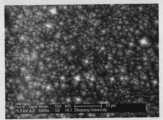
图1为实施例1制备的硅片表面形貌;Fig. 1 is the silicon chip surface morphology that embodiment 1 prepares;
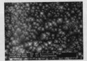
图2为实施例2制备的硅片表面形貌;Fig. 2 is the silicon chip surface morphology that embodiment 2 prepares;
图3为实施例3制备的硅片表面形貌;Fig. 3 is the silicon chip surface topography that embodiment 3 prepares;
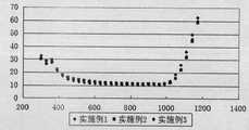
图4为85℃下硅片在含有NaClO和C2H5OH的制绒液中反应20分钟后表面反射率,其中NaClO的体积百分比浓度分别为15%、17%和20%,C2H5OH的浓度为10%。Figure 4 shows the surface reflectance of silicon wafers reacted in the texturing solution containing NaClO and C2 H5 OH for 20 minutes at 85°C, where the volume percentage concentrations of NaClO are 15%, 17% and 20%, and C2 H The concentration of5 OH was 10%.
具体实施方式Detailed ways
实施例1Example 1
配制混合液(制绒液),混合液的体积百分比组成为:Prepare mixed solution (texturing solution), the volume percentage of mixed solution consists of:
NaClO 15%NaClO 15%
C2H5OH 10%C2 H5 OH 10%
余量为水。The balance is water.
制绒液搅拌均匀后温度控制在85℃,将经过清洗的单晶硅片放入该制绒液中,反应20分钟,取出后用去离子水清洗,烘干。测得硅片单面腐蚀掉10微米,反射率为11.1%。After the texturing solution is evenly stirred, the temperature is controlled at 85° C., the cleaned monocrystalline silicon wafer is put into the texturing solution, reacted for 20 minutes, taken out, washed with deionized water, and dried. It was measured that the single side of the silicon wafer was etched away by 10 microns, and the reflectivity was 11.1%.
实施例2Example 2
配制混合液(制绒液),混合液的体积百分比组成为:Prepare mixed solution (texturing solution), the volume percentage of mixed solution consists of:
NaClO 17%NaClO 17%
C2H5OH 10%C2 H5 OH 10%
余量为水。The balance is water.
制绒液搅拌均匀后温度控制在85℃,将经过清洗的单晶硅片放入该制绒液中,反应20分钟,取出后用去离子水清洗,烘干。测得硅片单面厚度腐蚀掉11微米,反射率为12%。After the texturing solution is evenly stirred, the temperature is controlled at 85° C., the cleaned monocrystalline silicon wafer is put into the texturing solution, reacted for 20 minutes, taken out, washed with deionized water, and dried. It is measured that the thickness of one side of the silicon wafer is etched away by 11 microns, and the reflectivity is 12%.
实施例3Example 3
配制混合液(制绒液),混合液的体积百分比组成为:Prepare mixed solution (texturing solution), the volume percentage of mixed solution consists of:
NaClO 20%NaClO 20%
C2H5OH 10%C2 H5 OH 10%
余量为水。The balance is water.
制绒液搅拌均匀后温度控制在85℃,将经过清洗的单晶硅片放入该制绒液中,反应20分钟,取出后用去离子水清洗,烘干。测得硅片单面厚度腐蚀掉12.5微米,反射率为12.1%。After the texturing solution is evenly stirred, the temperature is controlled at 85° C., the cleaned monocrystalline silicon wafer is put into the texturing solution, reacted for 20 minutes, taken out, washed with deionized water, and dried. It is measured that the thickness of one side of the silicon wafer is etched away by 12.5 microns, and the reflectivity is 12.1%.
实施例4Example 4
配制混合液(制绒液),混合液的体积百分比组成为:Prepare mixed solution (texturing solution), the volume percentage of mixed solution consists of:
NaClO 17%NaClO 17%
C2H5OH 15%C2 H5 OH 15%
余量为水。The balance is water.
制绒液搅拌均匀后温度控制在85℃,将经过清洗的单晶硅片放入该制绒液中,反应20分钟,取出后用去离子水清洗,烘干。测得硅片单面厚度腐蚀掉8.5微米,反射率为14.1%。After the texturing solution is evenly stirred, the temperature is controlled at 85° C., the cleaned monocrystalline silicon wafer is put into the texturing solution, reacted for 20 minutes, taken out, washed with deionized water, and dried. It is measured that the thickness of one side of the silicon wafer is etched away by 8.5 microns, and the reflectivity is 14.1%.
实施例5Example 5
配制混合液(制绒液),混合液的体积百分比组成为:Prepare mixed solution (texturing solution), the volume percentage of mixed solution consists of:
NaClO 17%NaClO 17%
C2H5OH 10%C2 H5 OH 10%
余量为水。The balance is water.
制绒液搅拌均匀后温度控制在80℃,将经过清洗的单晶硅片放入该制绒液中,反应20分钟,取出后用去离子水清洗,烘干。测得硅片单面厚度腐蚀掉9.5微米,反射率为11.4%。After the texturing solution is evenly stirred, the temperature is controlled at 80° C., the cleaned monocrystalline silicon wafer is put into the texturing solution, reacted for 20 minutes, taken out, washed with deionized water, and dried. It is measured that the thickness of one side of the silicon wafer is etched away by 9.5 microns, and the reflectivity is 11.4%.
Claims (2)
Translated fromChinesePriority Applications (1)
| Application Number | Priority Date | Filing Date | Title |
|---|---|---|---|
| CN201010138362ACN101818348A (en) | 2010-04-02 | 2010-04-02 | Method for preparing texture of monocrystalline-silicon solar cell by one-step process |
Applications Claiming Priority (1)
| Application Number | Priority Date | Filing Date | Title |
|---|---|---|---|
| CN201010138362ACN101818348A (en) | 2010-04-02 | 2010-04-02 | Method for preparing texture of monocrystalline-silicon solar cell by one-step process |
Publications (1)
| Publication Number | Publication Date |
|---|---|
| CN101818348Atrue CN101818348A (en) | 2010-09-01 |
Family
ID=42653611
Family Applications (1)
| Application Number | Title | Priority Date | Filing Date |
|---|---|---|---|
| CN201010138362APendingCN101818348A (en) | 2010-04-02 | 2010-04-02 | Method for preparing texture of monocrystalline-silicon solar cell by one-step process |
Country Status (1)
| Country | Link |
|---|---|
| CN (1) | CN101818348A (en) |
Cited By (12)
| Publication number | Priority date | Publication date | Assignee | Title |
|---|---|---|---|---|
| CN102168315A (en)* | 2011-03-14 | 2011-08-31 | 中节能太阳能科技(镇江)有限公司 | Method for texturing surface of monocrystalline silicon solar battery |
| CN102569059A (en)* | 2011-12-26 | 2012-07-11 | 嘉兴优太太阳能有限公司 | Improved solar cell surface felting method |
| CN102560493A (en)* | 2012-01-18 | 2012-07-11 | 电子科技大学 | Method for preparing silicon nanowire array |
| CN105679862A (en)* | 2010-12-21 | 2016-06-15 | 西奥尼克斯公司 | Semiconductor devices having reduced substrate damage and associated methods |
| US10229951B2 (en) | 2010-04-21 | 2019-03-12 | Sionyx, Llc | Photosensitive imaging devices and associated methods |
| US10244188B2 (en) | 2011-07-13 | 2019-03-26 | Sionyx, Llc | Biometric imaging devices and associated methods |
| US10269861B2 (en) | 2011-06-09 | 2019-04-23 | Sionyx, Llc | Process module for increasing the response of backside illuminated photosensitive imagers and associated methods |
| US10347682B2 (en) | 2013-06-29 | 2019-07-09 | Sionyx, Llc | Shallow trench textured regions and associated methods |
| US10361232B2 (en) | 2009-09-17 | 2019-07-23 | Sionyx, Llc | Photosensitive imaging devices and associated methods |
| US10361083B2 (en) | 2004-09-24 | 2019-07-23 | President And Fellows Of Harvard College | Femtosecond laser-induced formation of submicrometer spikes on a semiconductor substrate |
| US10374109B2 (en) | 2001-05-25 | 2019-08-06 | President And Fellows Of Harvard College | Silicon-based visible and near-infrared optoelectric devices |
| US10505054B2 (en) | 2010-06-18 | 2019-12-10 | Sionyx, Llc | High speed photosensitive devices and associated methods |
Citations (2)
| Publication number | Priority date | Publication date | Assignee | Title |
|---|---|---|---|---|
| CN101540351A (en)* | 2009-04-14 | 2009-09-23 | 浙江大学 | Method for etching matte on surface of single crystal silicon solar energy battery |
| CN101599514A (en)* | 2009-07-10 | 2009-12-09 | 北京北方微电子基地设备工艺研究中心有限责任公司 | A kind of textured mono-crystalline silicon solar battery and preparation method thereof and preparation system |
- 2010
- 2010-04-02CNCN201010138362Apatent/CN101818348A/enactivePending
Patent Citations (2)
| Publication number | Priority date | Publication date | Assignee | Title |
|---|---|---|---|---|
| CN101540351A (en)* | 2009-04-14 | 2009-09-23 | 浙江大学 | Method for etching matte on surface of single crystal silicon solar energy battery |
| CN101599514A (en)* | 2009-07-10 | 2009-12-09 | 北京北方微电子基地设备工艺研究中心有限责任公司 | A kind of textured mono-crystalline silicon solar battery and preparation method thereof and preparation system |
Cited By (16)
| Publication number | Priority date | Publication date | Assignee | Title |
|---|---|---|---|---|
| US10374109B2 (en) | 2001-05-25 | 2019-08-06 | President And Fellows Of Harvard College | Silicon-based visible and near-infrared optoelectric devices |
| US10741399B2 (en) | 2004-09-24 | 2020-08-11 | President And Fellows Of Harvard College | Femtosecond laser-induced formation of submicrometer spikes on a semiconductor substrate |
| US10361083B2 (en) | 2004-09-24 | 2019-07-23 | President And Fellows Of Harvard College | Femtosecond laser-induced formation of submicrometer spikes on a semiconductor substrate |
| US10361232B2 (en) | 2009-09-17 | 2019-07-23 | Sionyx, Llc | Photosensitive imaging devices and associated methods |
| US10229951B2 (en) | 2010-04-21 | 2019-03-12 | Sionyx, Llc | Photosensitive imaging devices and associated methods |
| US10505054B2 (en) | 2010-06-18 | 2019-12-10 | Sionyx, Llc | High speed photosensitive devices and associated methods |
| CN105679862A (en)* | 2010-12-21 | 2016-06-15 | 西奥尼克斯公司 | Semiconductor devices having reduced substrate damage and associated methods |
| CN102168315B (en)* | 2011-03-14 | 2012-11-21 | 中节能太阳能科技(镇江)有限公司 | Method for texturing surface of monocrystalline silicon solar battery |
| CN102168315A (en)* | 2011-03-14 | 2011-08-31 | 中节能太阳能科技(镇江)有限公司 | Method for texturing surface of monocrystalline silicon solar battery |
| US10269861B2 (en) | 2011-06-09 | 2019-04-23 | Sionyx, Llc | Process module for increasing the response of backside illuminated photosensitive imagers and associated methods |
| US10244188B2 (en) | 2011-07-13 | 2019-03-26 | Sionyx, Llc | Biometric imaging devices and associated methods |
| CN102569059A (en)* | 2011-12-26 | 2012-07-11 | 嘉兴优太太阳能有限公司 | Improved solar cell surface felting method |
| CN102560493B (en)* | 2012-01-18 | 2013-10-30 | 电子科技大学 | Method for preparing silicon nanowire array |
| CN102560493A (en)* | 2012-01-18 | 2012-07-11 | 电子科技大学 | Method for preparing silicon nanowire array |
| US10347682B2 (en) | 2013-06-29 | 2019-07-09 | Sionyx, Llc | Shallow trench textured regions and associated methods |
| US11069737B2 (en) | 2013-06-29 | 2021-07-20 | Sionyx, Llc | Shallow trench textured regions and associated methods |
Similar Documents
| Publication | Publication Date | Title |
|---|---|---|
| CN101818348A (en) | Method for preparing texture of monocrystalline-silicon solar cell by one-step process | |
| CN101661972B (en) | Process for manufacturing monocrystalline silicon solar cell texture with low surface reflectivity | |
| WO2021136196A1 (en) | Monocrystalline silicon wafer with pyramid superposed structure | |
| CN102299207B (en) | Method for manufacturing porous pyramid-type silicon surface light trapping structure for solar cell | |
| CN101540351B (en) | A method of etching textured surface on the surface of monocrystalline silicon solar cell | |
| WO2015017956A1 (en) | Single-sided polishing method for monocrystalline silicon wafer used in solar battery | |
| WO2016019767A1 (en) | Acidic texturing solution for etching solar cell silicon wafer, texturing method, solar cell and manufacturing method for solar cell | |
| CN104993019A (en) | Preparation method of localized back contact solar cell | |
| CN102618937A (en) | Texture etching technology of single crystalline silicon solar cell | |
| CN102931290A (en) | Polycrystalline silicon solar cell reworking method without damaging suede | |
| CN106601862A (en) | Texturing method for reducing reflectivity of monocrystalline silicon heterojunction solar cell | |
| CN107919275A (en) | A method for making texturing at room temperature, and silicon wafers, solar cell sheets and preparation methods thereof | |
| CN114990700B (en) | Additive and process for preparing terrace pyramid microstructure silicon wafer and obtained silicon wafer | |
| CN104218122A (en) | Texturing method for decreasing polycrystalline silicon reflectivity during diamond wire cutting | |
| CN103789839B (en) | A kind of texturing method of weakly oxidized monocrystalline silicon wafer | |
| CN104393104B (en) | A kind for the treatment of technology for HIT solar cell texture | |
| CN204311157U (en) | For the silicon chip of solar cell | |
| CN111105995B (en) | A method for cleaning and texturing monocrystalline silicon wafers | |
| CN204167329U (en) | Metallurgy polycrystalline silicon solar battery sheet and solar panel | |
| CN205194713U (en) | A silicon chip for solar cell | |
| CN101714592A (en) | Manufacturing method of low-purity monocrystal silicon solar cell | |
| CN105826410A (en) | Diamond wire cutting trace eliminated polysilicon texturizing method | |
| CN119039886A (en) | Alkali polishing additive and alkali polishing liquid for improving double-sided efficiency of solar cell and application of alkali polishing additive and alkali polishing liquid | |
| CN106024970B (en) | The crystal silicon battery lithographic method and PERC battery acid polishing methods of hardware compatibility | |
| CN104716206A (en) | Method for improving defective product reworking conversion efficiency after battery is plated with antireflection film |
Legal Events
| Date | Code | Title | Description |
|---|---|---|---|
| C06 | Publication | ||
| PB01 | Publication | ||
| C10 | Entry into substantive examination | ||
| SE01 | Entry into force of request for substantive examination | ||
| C02 | Deemed withdrawal of patent application after publication (patent law 2001) | ||
| WD01 | Invention patent application deemed withdrawn after publication | Application publication date:20100901 |