CN101814503B - Complementary grid-controlled PNPN field effect transistor and preparation method thereof - Google Patents
Complementary grid-controlled PNPN field effect transistor and preparation method thereofDownload PDFInfo
- Publication number
- CN101814503B CN101814503BCN2010101417343ACN201010141734ACN101814503BCN 101814503 BCN101814503 BCN 101814503BCN 2010101417343 ACN2010101417343 ACN 2010101417343ACN 201010141734 ACN201010141734 ACN 201010141734ACN 101814503 BCN101814503 BCN 101814503B
- Authority
- CN
- China
- Prior art keywords
- type
- region
- forms
- semiconductor substrate
- low energy
- Prior art date
- Legal status (The legal status is an assumption and is not a legal conclusion. Google has not performed a legal analysis and makes no representation as to the accuracy of the status listed.)
- Expired - Fee Related
Links
Images


Landscapes
- Metal-Oxide And Bipolar Metal-Oxide Semiconductor Integrated Circuits (AREA)
Abstract
Translated fromChinese
Description
Translated fromChinese技术领域technical field
本发明属于半导体器件技术领域,具体涉及涉及一种互补栅控PNPN场效应晶体管及其制造方法。The invention belongs to the technical field of semiconductor devices, and in particular relates to a complementary gate-controlled PNPN field effect transistor and a manufacturing method thereof.
背景技术Background technique
随着半导体集成电路技术的不断发展,金属-氧化物-硅场效应晶体管(MOSFET)的尺寸越来越小,单位阵列上的晶体管密度也越来越高,随之而来的短沟道效应愈加明显。当沟道长度降低到45纳米以下时,MOSFET源漏极之间的漏电流,随着沟道长度的缩小而迅速上升,使得半导体芯片的性能劣化,甚至无法正常工作,因此,有必要使用新型的器件来获得较小的漏电流,从而降低芯片功耗。隧穿场效应晶体管和栅控PNPN场效应晶体管都是漏电流非常小的晶体管,可以大大降低半导体芯片的功耗。With the continuous development of semiconductor integrated circuit technology, the size of metal-oxide-silicon field-effect transistors (MOSFETs) is getting smaller and smaller, and the density of transistors on the unit array is getting higher and higher, and the short-channel effect that follows more and more obvious. When the channel length is reduced below 45 nanometers, the leakage current between the source and drain of the MOSFET increases rapidly as the channel length shrinks, which degrades the performance of the semiconductor chip and even fails to work normally. Therefore, it is necessary to use a new Devices to obtain a smaller leakage current, thereby reducing chip power consumption. Tunneling field effect transistors and gate-controlled PNPN field effect transistors are both transistors with very small leakage current, which can greatly reduce the power consumption of semiconductor chips.
图1显示了一种凹陷沟道的隧穿场效应晶体管结构,该隧穿场效应晶体管包括一个栅叠层区,一个源区、一个漏区和一个衬底区。栅叠层区由绝缘层105和导体层106构成。绝缘层105包括一层二氧化硅和一层高介电常数介质材料。导体层106包含一层多晶硅和一层金属。栅叠层区的侧墙107为绝缘介质,比如Si3N4。源区108的掺杂类型与漏区104的掺杂类型相反,并且与衬底103的掺杂类型相同。源区108和漏区104之间贴近绝缘层105的衬底表面为器件的凹陷沟道区域。衬底101和102为含轻掺杂n型或p型杂质的硅层,或为绝缘氧化层。绝缘层109为该隧穿场效应晶体管的钝化层,导体110、111和112为金属材料,作为该隧穿场效应晶体管的电极。凹陷沟道的使用,使得晶体管的沟道长度增加,抑制了漏电流的产生。FIG. 1 shows a structure of a tunneling field effect transistor with a recessed channel. The tunneling field effect transistor includes a gate stack region, a source region, a drain region and a substrate region. The gate stack region is composed of an
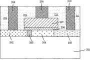
图2显示了一种平面沟道的栅控PNPN场效应晶体管结构。如图1所示,该栅控PNPN场效应晶体管在半导体衬底201上包含有:SiGe中掺杂的p型区域202和n型区域203,Si中掺杂的p型区域204和n型区域105。晶体管的栅极结构207形成于栅氧化层206之上。绝缘介质211为该晶体管的钝化层,所示208、209和210为金属材料,作为晶体管的电极。重掺杂的n型区域203是完全耗尽的一小块区域,用于增加晶体管横向的导电区域。掺杂区域202、203、204和205构成一个p-n-p-n结结构,可以降低晶体管中的漏电流。Figure 2 shows a gate-controlled PNPN field effect transistor structure with a planar channel. As shown in FIG. 1, the gated PNPN field effect transistor includes on a semiconductor substrate 201: a p-
尽管隧穿场效应晶体管和栅控PNPN场效应晶体管的漏电流要低于传统的MOS晶体管,可以大大降低芯片功耗。但是,随着半导体器件的尺寸缩小到20纳米以下,隧穿场效应晶体管和栅控PNPN场效应晶体管的漏电流也在随器件的缩小而迅速上升。普通隧穿场效应晶体管和栅控PNPN场效应晶体管的驱动电流较MOSFET要低2-3个数量级,因此需要提高其驱动电流,以提高其集成电路芯片的性能。Although the leakage current of tunneling field effect transistors and gate-controlled PNPN field effect transistors is lower than that of traditional MOS transistors, chip power consumption can be greatly reduced. However, as the size of semiconductor devices shrinks below 20 nanometers, the leakage current of tunneling field effect transistors and gate-controlled PNPN field effect transistors also increases rapidly with the shrinking of devices. The driving current of ordinary tunneling field effect transistors and gate-controlled PNPN field effect transistors is 2-3 orders of magnitude lower than that of MOSFETs, so it is necessary to increase their driving currents to improve the performance of their integrated circuit chips.
发明内容Contents of the invention
有鉴于此,本发明的目的在于提出一种新型的晶体管结构,该晶体管在提高驱动电流的同时,也可以抑制漏电流的增加。In view of this, the purpose of the present invention is to propose a novel transistor structure, which can suppress the increase of the leakage current while increasing the driving current.
为达到本发明的上述目的,本发明提出了一种源极为窄禁带宽度的凹陷沟道的互补栅控PNPN场效应晶体管,该互补栅控PNPN场效应晶体管包括一个半导体衬底、在所述半导体衬底上形成的一个源极为窄禁带宽度的凹陷沟道的N型栅控PNPN场效应晶体管和一个源极为窄禁带宽度的凹陷沟道的P型栅控PNPN场效应晶体管。In order to achieve the above-mentioned purpose of the present invention, the present invention proposes a complementary gate-controlled PNPN field-effect transistor whose source is a recessed channel with a narrow bandgap width, the complementary gate-controlled PNPN field-effect transistor comprises a semiconductor substrate, the An N-type gate-controlled PNPN field effect transistor whose source is a recessed channel with a narrow forbidden band width and a P-type gate-controlled PNPN field effect transistor whose source is a recessed channel with a narrow forbidden band width are formed on a semiconductor substrate.
进一步地,所述的N型栅控PNPN场效应晶体管包括:所述半导体衬底中的p型掺杂区域;在所述p型掺杂区域内形成的具有n型掺杂类型的漏区;在所述p型掺杂区域内靠近漏区的一侧形成的凹陷沟道区域;在所述p型掺杂区域内凹陷沟道的非漏区侧形成的具有n型掺杂类型的窄禁带宽度材料耗尽区;在所述窄禁带宽度材料耗尽区之上形成的具有p型掺杂类型的窄禁带宽度材料源区;在所述凹陷沟道区域之上形成的覆盖整个凹陷沟道区域的栅区;在所述栅区两侧形成的覆盖整个栅区两侧面的绝缘薄膜侧墙。Further, the N-type gate-controlled PNPN field effect transistor includes: a p-type doped region in the semiconductor substrate; a drain region with an n-type doped type formed in the p-type doped region; A recessed channel region formed on the side of the p-type doped region close to the drain region; a narrow forbidden region with an n-type doping type formed on the non-drain region side of the recessed channel in the p-type doped region a bandgap material depletion region; a narrow bandgap material source region having a p-type doping type formed above the narrow bandgap material depletion region; The gate region of the recessed channel region; the insulating film sidewalls formed on both sides of the gate region covering the entire two sides of the gate region.
更进一步地,所述的P型栅控PNPN场效应晶体管包括:所述半导体衬底中的n型掺杂区域;在所述n型掺杂区域内形成的具有p型掺杂类型的漏区;在所述n型掺杂区域内靠近漏区的一侧形成的凹陷沟道区域;在所述n型掺杂区域内凹陷沟道的非漏区侧形成的具有p型掺杂类型的窄禁带宽度材料耗尽区;在所述窄禁带宽度材料耗尽区之上形成的具有n型掺杂类型的窄禁带宽度材料源区;在所述凹陷沟道区域之上形成的覆盖整个凹陷沟道区域的栅区;在所述栅区两侧形成的覆盖整个栅区两侧面的绝缘薄膜侧墙。Furthermore, the P-type gate-controlled PNPN field effect transistor includes: an n-type doped region in the semiconductor substrate; a drain region with a p-type doped type formed in the n-type doped region a recessed channel region formed on a side close to the drain region in the n-type doped region; a narrow channel with a p-type doping type formed on the non-drain region side of the recessed channel in the n-type doped region a bandgap material depletion region; a narrow bandgap material source region having an n-type doping type formed over the narrow bandgap material depletion region; a covering formed over the recessed channel region The gate region of the entire recessed channel region; the insulating film sidewalls formed on both sides of the gate region covering the entire two sides of the gate region.
对于N型栅控PNPN场效应晶体管,窄禁带宽度材料采用SiGe或者Ge;对于P型栅控PNPN场效应晶体管,窄禁带宽度材料采用AsGa或者InAsGa。由于采用了窄禁带宽度材料,晶体管的驱动电流得到上升。同时,凹陷沟道的使用,使得晶体管的沟道长度增长,抑制了漏电流的产生。For N-type gate-controlled PNPN field effect transistors, SiGe or Ge is used as the narrow bandgap material; for P-type gate-controlled PNPN field effect transistors, AsGa or InAsGa is used as the narrow bandgap material. Due to the use of narrow bandgap materials, the driving current of the transistor is increased. At the same time, the use of the recessed channel increases the channel length of the transistor and suppresses the generation of leakage current.
本发明还提出了这种使用窄禁带宽度材料的凹陷沟道的互补栅控PNPN场效应晶体管结构的制造方法,具体步骤如下:The present invention also proposes a method for manufacturing a complementary gate-controlled PNPN field-effect transistor structure using a recessed channel of a narrow bandgap material, and the specific steps are as follows:
提供一个具有第一种和第二种掺杂类型的半导体衬底;providing a semiconductor substrate having first and second doping types;
淀积形成第一层光刻胶,并通过掩膜曝光光刻出需掺杂的图形;Deposit and form the first layer of photoresist, and expose the pattern to be doped by mask exposure;
进行离子注入,在所述半导体衬底第一种掺杂类型区域内形成第二种掺杂类型的区域;performing ion implantation to form a region of the second doping type in the region of the first doping type of the semiconductor substrate;
第一层光刻胶剥离;The first layer of photoresist is stripped;
淀积形成第二层光刻胶,并通过掩膜曝光光刻出需掺杂的图形;Deposit and form the second layer of photoresist, and expose the pattern to be doped by mask exposure;
再次进行离子注入,在所述半导体衬底第二种掺杂类型区域内形成第一种掺杂类型的区域;performing ion implantation again to form a region of the first doping type in the region of the second doping type of the semiconductor substrate;
第二层光刻胶剥离;The second layer of photoresist is stripped;
依次淀积形成第一层硬质掩膜和第三层光刻胶;Depositing and forming the first layer of hard mask and the third layer of photoresist in sequence;
掩膜曝光刻蚀暴露出衬底,并刻蚀衬底形成器件的凹陷沟道结构;Mask exposure etching exposes the substrate, and etches the substrate to form the recessed channel structure of the device;
第三层光刻胶和第一层硬质掩膜剥离;The third layer of photoresist and the first layer of hard mask are stripped;
依次形成第一种绝缘薄膜、第二种绝缘薄膜、第一种导电薄膜、第二种导电薄膜和第四层光刻胶;sequentially forming a first insulating film, a second insulating film, a first conductive film, a second conductive film and a fourth layer of photoresist;
掩膜曝光刻蚀形成器件的栅极结构;Mask exposure etching to form the gate structure of the device;
第四层光刻胶剥离;The fourth layer of photoresist is stripped;
依次淀积形成第三种绝缘薄膜和第五层光刻胶;Depositing and forming the third insulating film and the fifth layer of photoresist in sequence;
第一次选择性刻蚀以露出硅衬底;The first selective etch to expose the silicon substrate;
反应离子刻蚀硅衬底;Reactive ion etching of silicon substrates;
继续对硅衬底进行各向同性刻蚀;Continue to perform isotropic etching on the silicon substrate;
第五层光刻胶剥离;The fifth layer of photoresist is stripped;
外延形成一层具有第二种掺杂类型的第一种窄禁带宽度材料的耗尽区;Epitaxially forming a layer of depletion region of the first narrow bandgap material with the second doping type;
外延形成一层具有第一种掺杂类型的第一种窄禁带宽度材料区域;Epitaxially forming a layer of a first narrow bandgap material region with a first doping type;
淀积形成第六层光刻胶;Depositing and forming the sixth layer of photoresist;
第二次选择性刻蚀以露出硅衬底;The second selective etching to expose the silicon substrate;
反应离子刻蚀硅衬底;Reactive ion etching of silicon substrates;
继续对硅衬底进行各向同性刻蚀;Continue to perform isotropic etching on the silicon substrate;
第六层光刻胶剥离;The sixth layer of photoresist is stripped;
外延形成一层具有第一种掺杂类型的第二种窄禁带宽度材料的耗尽区;Epitaxially forming a depletion region of a second narrow bandgap material with the first doping type;
外延形成一层具有第二种掺杂类型的第二种窄禁带宽度材料区域;Epitaxially forming a layer of a second narrow bandgap material region with a second doping type;
刻蚀第三种绝缘薄膜形成侧墙结构;Etching the third insulating film to form a sidewall structure;
刻蚀掉多余的第二种绝缘薄膜;Etching away the redundant second insulating film;
淀积形成第四种绝缘薄膜;Depositing and forming a fourth insulating film;
对四种绝缘薄膜进行刻蚀形成通孔;Etching the four insulating films to form through holes;
淀积第三种导电薄膜形成电极。A third conductive film is deposited to form electrodes.
进一步地,所述的半导体衬底为单晶硅、多晶硅或者绝缘体上的硅(SOI)。所述的第一种硬质掩膜为氧化硅或者氮化硅。所述第一种绝缘薄膜为氧化硅。所述第二层绝缘薄膜为高介电常数介质,可以为氧化铪、氧化锆、或为氧化镧、或为氧化钽、或为氧化锶、或为氧化铱。所述第三种、第四种绝缘薄膜为氧化硅、氮化硅或者为它们之间相混合的绝缘材料。所述第一种导电材料为氮化钛、氮化钽或者金属硅化物。所述第二种导电材料为掺杂的多晶硅。所述第三种导电薄膜为金属铝、金属钨或者为其它金属导电材料。Further, the semiconductor substrate is single crystal silicon, polycrystalline silicon or silicon on insulator (SOI). The first hard mask is silicon oxide or silicon nitride. The first insulating film is silicon oxide. The second layer of insulating film is a high dielectric constant dielectric, which may be hafnium oxide, zirconium oxide, or lanthanum oxide, or tantalum oxide, or strontium oxide, or iridium oxide. The third and fourth insulating films are silicon oxide, silicon nitride or insulating materials mixed therebetween. The first conductive material is titanium nitride, tantalum nitride or metal silicide. The second conductive material is doped polysilicon. The third conductive film is metal aluminum, metal tungsten or other metal conductive materials.
更进一步地,所述的第一种掺杂类型为n型,第二种掺杂类型为p型,所述第一种窄禁带宽度材料为SiGe或者Ge,第二种窄禁带宽度材料为AsGa或者InAsGa;或者,所述的第一种掺杂类型为p型,第二种掺杂类型为n型,所述第一种窄禁带宽度材料为AsGa或者InAsGa,第二种窄禁带宽度材料为SiGe或者Ge。Furthermore, the first doping type is n-type, the second doping type is p-type, the first narrow bandgap material is SiGe or Ge, and the second narrow bandgap material is is AsGa or InAsGa; or, the first doping type is p-type, the second doping type is n-type, the first narrow bandgap material is AsGa or InAsGa, and the second narrow bandgap material is The tape width material is SiGe or Ge.
本发明提出的使用窄禁带宽度的凹陷沟道的互补栅控PNPN场效应晶体管在提高驱动电流的同时漏电流也得到减小,而且,这种类似CMOS的互补栅控PNPN场效应晶体管可以实现低功耗高性能的集成电路芯片。The complementary gate-controlled PNPN field effect transistor using the recessed channel with a narrow bandgap width proposed by the present invention can reduce the leakage current while increasing the drive current, and this CMOS-like complementary gate-controlled PNPN field effect transistor can realize Integrated circuit chip with low power consumption and high performance.
附图说明Description of drawings
图1为现有的一种凹陷沟道的隧穿场效应晶体管结构的截面图。FIG. 1 is a cross-sectional view of a conventional structure of a tunneling field effect transistor with a recessed channel.
图2为现有的一个平面沟道的n型栅控PNPN场效应晶体管结构的截面图。FIG. 2 is a cross-sectional view of an existing n-type gate-controlled PNPN field effect transistor structure with a planar channel.
图3至图12为本发明提供的一个凹陷沟道的互补栅控PNPN场效应晶体管结构的实施工艺的截面图。3 to 12 are cross-sectional views of the implementation process of a recessed channel complementary gate-controlled PNPN field effect transistor structure provided by the present invention.
具体实施方式Detailed ways
下面将参照附图对本发明的一个示例性实施方式作详细说明。在图中,为了方便说明,放大了层和区域的厚度,所示大小并不代表实际尺寸。尽管这些图并不是完全准确的反映出器件的实际尺寸,但是它们还是完整的反映了区域和组成结构之间的相互位置,特别是组成结构之间的上下和相邻关系。An exemplary embodiment of the present invention will be described in detail below with reference to the accompanying drawings. In the drawings, the thicknesses of layers and regions are exaggerated for convenience of illustration, and the shown sizes do not represent actual sizes. Although these figures do not completely reflect the actual size of the device, they still fully reflect the mutual positions between the regions and the constituent structures, especially the upper-lower and adjacent relationships between the constituent structures.
参考图是本发明的理想化实施例的示意图,本发明所示的实施例不应该被认为仅限于图中所示区域的特定形状,而是包括所得到的形状,比如制造引起的偏差。同时在下面的描述中,所使用的术语晶片和衬底可以理解为包括正在工艺加工中的半导体晶片,可能包括在其上所制备的其它薄膜层。The referenced figures are schematic illustrations of idealized embodiments of the invention, and the illustrated embodiments of the invention should not be construed as limited to the particular shapes of regions illustrated in the figures but are to include resulting shapes, such as manufacturing-induced deviations. Also in the following description, the terms wafer and substrate used may be understood to include the semiconductor wafer being processed, possibly including other thin film layers prepared thereon.
首先,在提供的半导体衬底上淀积形成一层光刻胶301,并通过掩膜曝光光刻出需掺杂的图形,然后进行n型杂质离子注入形成掺杂的区域302,如图3。其中,衬底300a和300b为含轻掺杂n型或者p型杂质的硅层,或为绝缘氧化层;衬底300c为轻掺杂p型杂质的硅层;衬底300d为轻掺杂n型杂质的硅层;衬底300e为形成的浅槽隔离结构。First, deposit and form a layer of
接下来,剥离光刻胶301,再淀积形成一层光刻胶303,并通过掩膜曝光光刻出需掺杂的图形,然后进行p型杂质离子注入形成掺杂的区域304,如图4。Next, the
接下来,剥离光刻胶303,再淀积形成一层硬质掩膜305,比如为二氧化硅,然后淀积一层光刻胶306,最后掩膜、曝光、刻蚀形成器件的凹陷沟道区域307a和307b,其结构如图5所示。在该刻蚀过程中采用干法刻蚀与湿法刻蚀相结合的刻蚀方法。Next, the photoresist 303 is stripped, and then deposited to form a layer of
接下来,先剥离光刻胶306,再刻蚀掉硬质掩膜305,然后热生长一层二氧化硅薄膜308,再淀积形成一层高介电常数介质309,如氧化铪,再淀积一层金属310,比如为TiN或为TaN,再淀积一层多晶硅311,再淀积一层光刻胶,然后通过掩膜、曝光、刻蚀形成器件的栅区,最后剥离光刻胶,形成的结构如图6所示。Next, the
接下来,淀积形成一层绝缘薄膜312,比如为二氧化硅或者氮化硅,再淀积形成一层光刻胶313,然后掩膜曝光光刻出需要的图形,再对绝缘薄膜312和高介电常数介质309进行刻蚀以露出硅衬底,再通过反应离子刻蚀硅衬底,最后对硅衬底进行各向同性刻蚀,形成如图7所示的结构。Next, deposit and form a layer of insulating
接下来,剥除光刻胶313,然后通过外延形成一层具有n型掺杂的第一种窄禁带宽度材料区域314,再通过外延形成一层具有p型掺杂的第一种窄禁带宽度材料区域315,如图8。第一种窄禁带宽度材料可以为SiGe或者Ge。Next, the
接下来,淀积形成一层光刻胶316,然后掩膜曝光光刻出需要的图形,再对绝缘薄膜312和高介电常数介质309进行刻蚀以露出硅衬底,再通过反应离子刻蚀硅衬底,最后对硅衬底进行各向同性刻蚀,形成如图9所示的结构。Next, a layer of
接下来,剥除光刻胶316,然后通过外延形成一层具有p型掺杂的第二种窄禁带宽度材料区域317,再通过外延形成一层具有n型掺杂的第二种窄禁带宽度材料区域318,如图10。第二种窄禁带宽度材料可以为AsGa或者InAsGa。Next, the
再接下来,对绝缘薄膜312进行刻蚀形成侧墙结构,再刻蚀掉多余的的高介电常数介质309,如图11所示。Next, the insulating
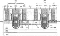
最后,淀积一层绝缘介质319,绝缘材料可以为氧化硅或为氮化硅,再淀积一层光刻胶,然后通过掩膜、曝光、刻蚀的方法形成通孔,并将光刻胶剥离,接着再淀积一层金属,可以为铝或者钨,然后刻蚀形成器件的电极320a、320b、320c、320d、320e和320f,最终形成如图8所示的器件结构。如图8,所示401为一个凹陷沟道的N型栅控PNPN场效应晶体管,所示402为一个凹陷沟道的P型栅控PNPN场效应晶体管。Finally, a layer of insulating
如上所述,在不偏离本发明精神和范围的情况下,还可以构成许多有很大差别的实施例。应当理解,除了如所附的权利要求所限定的,本发明不限于在说明书中所述的具体实例。As mentioned above, many widely different embodiments can be constructed without departing from the spirit and scope of the present invention. It should be understood that the invention is not limited to the specific examples described in the specification, except as defined in the appended claims.
Claims (16)
Priority Applications (1)
| Application Number | Priority Date | Filing Date | Title |
|---|---|---|---|
| CN2010101417343ACN101814503B (en) | 2010-04-08 | 2010-04-08 | Complementary grid-controlled PNPN field effect transistor and preparation method thereof |
Applications Claiming Priority (1)
| Application Number | Priority Date | Filing Date | Title |
|---|---|---|---|
| CN2010101417343ACN101814503B (en) | 2010-04-08 | 2010-04-08 | Complementary grid-controlled PNPN field effect transistor and preparation method thereof |
Publications (2)
| Publication Number | Publication Date |
|---|---|
| CN101814503A CN101814503A (en) | 2010-08-25 |
| CN101814503Btrue CN101814503B (en) | 2012-05-23 |
Family
ID=42621693
Family Applications (1)
| Application Number | Title | Priority Date | Filing Date |
|---|---|---|---|
| CN2010101417343AExpired - Fee RelatedCN101814503B (en) | 2010-04-08 | 2010-04-08 | Complementary grid-controlled PNPN field effect transistor and preparation method thereof |
Country Status (1)
| Country | Link |
|---|---|
| CN (1) | CN101814503B (en) |
Families Citing this family (2)
| Publication number | Priority date | Publication date | Assignee | Title |
|---|---|---|---|---|
| CN101834210A (en)* | 2010-04-28 | 2010-09-15 | 复旦大学 | A kind of PNPN field effect transistor with recessed channel and its preparation method |
| CN101894840A (en)* | 2010-07-08 | 2010-11-24 | 复旦大学 | Integrated circuit of concave channel type PNPN field effect transistor and manufacturing method thereof |
Citations (1)
| Publication number | Priority date | Publication date | Assignee | Title |
|---|---|---|---|---|
| CN101300665A (en)* | 2005-10-31 | 2008-11-05 | 美光科技公司 | Hidden channel negative differential resistance based memory cell |
Family Cites Families (2)
| Publication number | Priority date | Publication date | Assignee | Title |
|---|---|---|---|---|
| US8035126B2 (en)* | 2007-10-29 | 2011-10-11 | International Business Machines Corporation | One-transistor static random access memory with integrated vertical PNPN device |
| US7859051B2 (en)* | 2008-08-19 | 2010-12-28 | Infineon Technologies Austria Ag | Semiconductor device with a reduced band gap and process |
- 2010
- 2010-04-08CNCN2010101417343Apatent/CN101814503B/ennot_activeExpired - Fee Related
Patent Citations (1)
| Publication number | Priority date | Publication date | Assignee | Title |
|---|---|---|---|---|
| CN101300665A (en)* | 2005-10-31 | 2008-11-05 | 美光科技公司 | Hidden channel negative differential resistance based memory cell |
Also Published As
| Publication number | Publication date |
|---|---|
| CN101814503A (en) | 2010-08-25 |
Similar Documents
| Publication | Publication Date | Title |
|---|---|---|
| CN101819975B (en) | Vertical channel dual-grate tunneling transistor and preparation method thereof | |
| US20210167190A1 (en) | Semiconductor device, and manufacturing method thereof | |
| WO2011066730A1 (en) | Hybrid crystal orientation inversion mode gate-all-around cmos field effect transistor | |
| CN103872132A (en) | Metal-oxide-semiconductor transistor (MOS) and method of fabricating same | |
| CN101916782A (en) | Recessed channel transistor using ferroelectric material and manufacturing method thereof | |
| WO2011066728A1 (en) | Comound material accumulation type of whole enclosing gate cmos field effect transistor | |
| US20210202322A1 (en) | Semiconductor device | |
| CN103151383B (en) | A kind of U-shaped raceway groove tunneling transistor with laminated construction and preparation method thereof | |
| CN115172274A (en) | Preparation method of semiconductor device with heterogeneous mixed channel structure | |
| CN101834210A (en) | A kind of PNPN field effect transistor with recessed channel and its preparation method | |
| US20190312109A1 (en) | Field-effect transistors with a composite channel | |
| CN101814503B (en) | Complementary grid-controlled PNPN field effect transistor and preparation method thereof | |
| CN113838803B (en) | Semiconductor structure and method for forming the same | |
| US20070257322A1 (en) | Hybrid Transistor Structure and a Method for Making the Same | |
| CN110120418B (en) | Vertical nanowire transistor and method of forming the same | |
| US8586432B2 (en) | Method for manufacturing vertical-channel tunneling transistor | |
| US20230402520A1 (en) | Staircase stacked field effect transistor | |
| CN101894866B (en) | Impact ionization type field effect transistor of concave channel and manufacturing method thereof | |
| CN101807601A (en) | Grid-control PNPN field-effect transistor by utilizing SiGe source electrode and preparation method thereof | |
| CN102044433B (en) | A hybrid source-drain field-effect transistor and its preparation method | |
| CN101866858B (en) | Manufacture method of sinking channel type PNPN field effect transistor | |
| TW202240892A (en) | Semiconductor devices | |
| US7105391B2 (en) | Planar pedestal multi gate device | |
| CN113013164B (en) | Semiconductor device and manufacturing method thereof | |
| US20250204026A1 (en) | Semiconductor device with lateral diodes and stacked fets |
Legal Events
| Date | Code | Title | Description |
|---|---|---|---|
| C06 | Publication | ||
| PB01 | Publication | ||
| C10 | Entry into substantive examination | ||
| SE01 | Entry into force of request for substantive examination | ||
| C14 | Grant of patent or utility model | ||
| GR01 | Patent grant | ||
| CF01 | Termination of patent right due to non-payment of annual fee | ||
| CF01 | Termination of patent right due to non-payment of annual fee | Granted publication date:20120523 Termination date:20170408 |