CN101809530A - Integrated capacitive sensing apparatus and method - Google Patents
Integrated capacitive sensing apparatus and methodDownload PDFInfo
- Publication number
- CN101809530A CN101809530ACN200880108329ACN200880108329ACN101809530ACN 101809530 ACN101809530 ACN 101809530ACN 200880108329 ACN200880108329 ACN 200880108329ACN 200880108329 ACN200880108329 ACN 200880108329ACN 101809530 ACN101809530 ACN 101809530A
- Authority
- CN
- China
- Prior art keywords
- line
- alignment
- touch panel
- induction field
- panel device
- Prior art date
- Legal status (The legal status is an assumption and is not a legal conclusion. Google has not performed a legal analysis and makes no representation as to the accuracy of the status listed.)
- Pending
Links
Images


Classifications
- G—PHYSICS
- G06—COMPUTING OR CALCULATING; COUNTING
- G06F—ELECTRIC DIGITAL DATA PROCESSING
- G06F3/00—Input arrangements for transferring data to be processed into a form capable of being handled by the computer; Output arrangements for transferring data from processing unit to output unit, e.g. interface arrangements
- G06F3/01—Input arrangements or combined input and output arrangements for interaction between user and computer
- G06F3/03—Arrangements for converting the position or the displacement of a member into a coded form
- G06F3/041—Digitisers, e.g. for touch screens or touch pads, characterised by the transducing means
- G06F3/0412—Digitisers structurally integrated in a display
- G—PHYSICS
- G06—COMPUTING OR CALCULATING; COUNTING
- G06F—ELECTRIC DIGITAL DATA PROCESSING
- G06F3/00—Input arrangements for transferring data to be processed into a form capable of being handled by the computer; Output arrangements for transferring data from processing unit to output unit, e.g. interface arrangements
- G06F3/01—Input arrangements or combined input and output arrangements for interaction between user and computer
- G06F3/03—Arrangements for converting the position or the displacement of a member into a coded form
- G06F3/041—Digitisers, e.g. for touch screens or touch pads, characterised by the transducing means
- G06F3/044—Digitisers, e.g. for touch screens or touch pads, characterised by the transducing means by capacitive means
- G—PHYSICS
- G06—COMPUTING OR CALCULATING; COUNTING
- G06F—ELECTRIC DIGITAL DATA PROCESSING
- G06F3/00—Input arrangements for transferring data to be processed into a form capable of being handled by the computer; Output arrangements for transferring data from processing unit to output unit, e.g. interface arrangements
- G06F3/01—Input arrangements or combined input and output arrangements for interaction between user and computer
- G06F3/03—Arrangements for converting the position or the displacement of a member into a coded form
- G06F3/041—Digitisers, e.g. for touch screens or touch pads, characterised by the transducing means
- G06F3/0416—Control or interface arrangements specially adapted for digitisers
- G06F3/04164—Connections between sensors and controllers, e.g. routing lines between electrodes and connection pads
- G—PHYSICS
- G06—COMPUTING OR CALCULATING; COUNTING
- G06F—ELECTRIC DIGITAL DATA PROCESSING
- G06F3/00—Input arrangements for transferring data to be processed into a form capable of being handled by the computer; Output arrangements for transferring data from processing unit to output unit, e.g. interface arrangements
- G06F3/01—Input arrangements or combined input and output arrangements for interaction between user and computer
- G06F3/03—Arrangements for converting the position or the displacement of a member into a coded form
- G06F3/041—Digitisers, e.g. for touch screens or touch pads, characterised by the transducing means
- G06F3/0416—Control or interface arrangements specially adapted for digitisers
- G06F3/04166—Details of scanning methods, e.g. sampling time, grouping of sub areas or time sharing with display driving
- G—PHYSICS
- G06—COMPUTING OR CALCULATING; COUNTING
- G06F—ELECTRIC DIGITAL DATA PROCESSING
- G06F3/00—Input arrangements for transferring data to be processed into a form capable of being handled by the computer; Output arrangements for transferring data from processing unit to output unit, e.g. interface arrangements
- G06F3/01—Input arrangements or combined input and output arrangements for interaction between user and computer
- G06F3/03—Arrangements for converting the position or the displacement of a member into a coded form
- G06F3/041—Digitisers, e.g. for touch screens or touch pads, characterised by the transducing means
- G06F3/044—Digitisers, e.g. for touch screens or touch pads, characterised by the transducing means by capacitive means
- G06F3/0446—Digitisers, e.g. for touch screens or touch pads, characterised by the transducing means by capacitive means using a grid-like structure of electrodes in at least two directions, e.g. using row and column electrodes
- G—PHYSICS
- G06—COMPUTING OR CALCULATING; COUNTING
- G06F—ELECTRIC DIGITAL DATA PROCESSING
- G06F2203/00—Indexing scheme relating to G06F3/00 - G06F3/048
- G06F2203/041—Indexing scheme relating to G06F3/041 - G06F3/045
- G06F2203/04101—2.5D-digitiser, i.e. digitiser detecting the X/Y position of the input means, finger or stylus, also when it does not touch, but is proximate to the digitiser's interaction surface and also measures the distance of the input means within a short range in the Z direction, possibly with a separate measurement setup
- G—PHYSICS
- G06—COMPUTING OR CALCULATING; COUNTING
- G06F—ELECTRIC DIGITAL DATA PROCESSING
- G06F2203/00—Indexing scheme relating to G06F3/00 - G06F3/048
- G06F2203/041—Indexing scheme relating to G06F3/041 - G06F3/045
- G06F2203/04108—Touchless 2D- digitiser, i.e. digitiser detecting the X/Y position of the input means, finger or stylus, also when it does not touch, but is proximate to the digitiser's interaction surface without distance measurement in the Z direction
- G—PHYSICS
- G06—COMPUTING OR CALCULATING; COUNTING
- G06F—ELECTRIC DIGITAL DATA PROCESSING
- G06F2203/00—Indexing scheme relating to G06F3/00 - G06F3/048
- G06F2203/041—Indexing scheme relating to G06F3/041 - G06F3/045
- G06F2203/04111—Cross over in capacitive digitiser, i.e. details of structures for connecting electrodes of the sensing pattern where the connections cross each other, e.g. bridge structures comprising an insulating layer, or vias through substrate
Landscapes
- Engineering & Computer Science (AREA)
- General Engineering & Computer Science (AREA)
- Theoretical Computer Science (AREA)
- Human Computer Interaction (AREA)
- Physics & Mathematics (AREA)
- General Physics & Mathematics (AREA)
- Computer Networks & Wireless Communication (AREA)
- Position Input By Displaying (AREA)
- Control Of Indicators Other Than Cathode Ray Tubes (AREA)
- Devices For Indicating Variable Information By Combining Individual Elements (AREA)
- Liquid Crystal (AREA)
Abstract
Description
Translated fromChinese技术领域technical field
所公开的是一种触摸屏显示装置,并且更具体地是反转的底部栅极结构的薄膜晶体管液晶显示器的集成的电容性感测装置和方法,用于在所述装置的表面和感测线处感应电场以检测分路的电场线,从而确定物体在表面处的位置。Disclosed is an integrated capacitive sensing device and method for a touch screen display device, and more particularly an inverted bottom gate structure thin film transistor liquid crystal display, at the surface and sense lines of the device The electric field is sensed to detect the shunted electric field lines to determine the position of the object at the surface.
背景技术Background technique
移动通信装置的制造商——包括蜂窝电话的制造商——正在越来越多地向他们的装置增加功能。虽然有包含更多特征和对当前特征的改进的趋势,但是也有更小的移动通信装置的趋势。随着移动通信装置技术不断地改进,这些装置已经变得越来越小和越来越薄。因此,当在更小的装置中添加新特征和对当前特征作出改进时,期望更少和/或更小的硬件和软件组件。更少的硬件组件可以向消费者提供成本效益。Manufacturers of mobile communication devices, including manufacturers of cellular telephones, are increasingly adding functionality to their devices. While there is a trend to include more features and improvements over current features, there is also a trend to smaller mobile communication devices. As mobile communication device technology continues to improve, these devices have become smaller and thinner. Accordingly, fewer and/or smaller hardware and software components are desired when adding new features and making improvements to current features in smaller devices. Fewer hardware components can provide cost benefits to consumers.
诸如触摸屏的特征可以改善例如在移动通信装置以及其他类型的电子装置上的显示菜单操纵和游戏中的用户的体验。传统的触摸屏是使用在附加玻璃层或者塑料层上的电阻性或者电容性感测元件来实现的。所述附加触摸板玻璃层增加了较大的厚度,降低了亮度,并且可能使得显示器看起来微黄。而且,在电阻性设计中,也通常可见隔离物,降低了装置的美观。Features such as touch screens can improve a user's experience in display menu manipulation and gaming, for example, on mobile communication devices as well as other types of electronic devices. Traditional touch screens are implemented using resistive or capacitive sensing elements on an additional layer of glass or plastic. The additional layer of touchpad glass adds significant thickness, reduces brightness, and may make the display appear yellowish. Also, in resistive designs, spacers are also often visible, detracting from the aesthetics of the device.
没有使用附加层的薄设计触摸屏是使用例如在薄膜晶体管液晶显示器(TFT)阵列中的集成光电传感器来实现的。这样的实现由于降低了像素孔径比而大大地降低了显示亮度,并且需要复杂的感测算法以及限制性的配色方案。另外,在TFT阵列中的集成光电传感器可以仅仅一次感测一个触点。其他薄设计触摸屏包括感测玻璃移动的内部元件间隙电容性感测。再次,通过这种实现,大大降低显示亮度并且分辨率受限。Thin design touch screens without the use of additional layers are realized using integrated photosensors such as in thin film transistor liquid crystal display (TFT) arrays. Such implementations greatly reduce display brightness due to reduced pixel aperture ratios, and require complex sensing algorithms as well as restrictive color schemes. Additionally, the integrated photosensor in the TFT array can only sense one contact at a time. Other thin design touchscreens include internal element gap capacitive sensing that senses glass movement. Again, with this implementation, display brightness is greatly reduced and resolution is limited.
附图说明Description of drawings
图1图示了包括反转的底部栅极结构的低温多晶硅薄膜晶体管(LTPS TFT)显示器的一个像素,其中,所述底部栅极结构被翻起使得所述栅极现在面向外部;Figure 1 illustrates a pixel of a low temperature polysilicon thin film transistor (LTPS TFT) display comprising an inverted bottom gate structure, wherein the bottom gate structure is flipped up so that the gate now faces outward;
图2图示了显示装置的一部分和诸如手指或者触针的物体;Fig. 2 illustrates a part of a display device and an object such as a finger or a stylus;
图3图示了与显示装置的上表面相邻的TFT LCD显示矩阵的一部分的实施例,其中,栅极驱动器和激励开关在列线上,并且感测线是交替的列线;Figure 3 illustrates an embodiment of a portion of a TFT LCD display matrix adjacent to the upper surface of the display device, wherein the gate drivers and drive switches are on column lines and the sense lines are alternating column lines;
图4图示了另一个实施例,其中,栅极驱动器分别交织在交替的行线上,并且激励开关在奇数行线上且感测线在偶数行线上;Figure 4 illustrates another embodiment in which the gate drivers are individually interleaved on alternating row lines and the actuation switches are on odd row lines and the sense lines are on even row lines;
图5是针对接收到的分路检测的显示器和激励输出的时序图;以及Figure 5 is a timing diagram of display and stimulus outputs for received shunt detection; and
图6图示了触摸感测算法,其中,感测线可以在例如x方向的一个方向上并且然后在另一个方向y方向上扫描。Figure 6 illustrates a touch sensing algorithm, where a sense line can be scanned in one direction, eg x-direction, and then in another direction, y-direction.
具体实施方式Detailed ways
具体地,在薄设计触摸屏中,避免显示亮度的降低是有益的。当在更小和更薄的装置中添加新的特征和对当前特征进行改进时,包括更少的硬件和软件组件是进一步有益的。具体地,有益的是,可能用最少地附加硬件或者软件组件,使得基本上不增加装置尺寸和/或复杂性,重新使用已经作为装置的一部分的组件。In particular, in thin design touch screens, it is beneficial to avoid a decrease in display brightness. Including fewer hardware and software components is a further benefit when adding new features and improving upon current features in smaller and thinner devices. In particular, it may be beneficial to reuse components already part of the device with minimal additional hardware or software components, such that the device does not substantially increase size and/or complexity.
所公开的是触摸屏装置和用于感测在触摸屏装置的表面附近的物体的方法。如下面将详细描述的,电容性传感器通过下述方式被集成到显示电子装置中:通过将具有底部栅极结构的传统薄膜晶体管液晶显示器(TFT)层叠结构翻起,使得如下面将更详细描述的,TFT是反转的底部栅极结构,即,栅极面向外部。因此,所述栅极结构在显示器的顶部附近,并且除了栅极驱动线的作为显示线的功能之外,还将栅极驱动线重新用作激励线。因此,激励线驱动激励,以在显示装置的表面产生感应电场。另外,其他线被用作传感器线,使得传感器信号被输入到装置控制器,以确定物体在显示装置的表面处的位置。因此,扫描激励线以检测手指或者其他物体的存在。在翻起传统的TFT层叠结构使得它是反转的底部栅极结构并且如上所述重新使用该硬件时,不影响显示器的厚度,并且因此不影响所述装置的厚度。Disclosed are touch screen devices and methods for sensing objects near a surface of the touch screen device. As will be described in more detail below, capacitive sensors are integrated into display electronics by flipping a conventional thin film transistor liquid crystal display (TFT) stack structure with a bottom gate structure such that, as described in more detail below, Yes, the TFT is an inverted bottom gate structure, i.e., the gate faces outward. Thus, the gate structure is near the top of the display and reuses the gate drive lines as excitation lines in addition to their function as display lines. Accordingly, the excitation lines drive the excitation to generate an induced electric field on the surface of the display device. In addition, other wires are used as sensor wires so that sensor signals are input to the device controller to determine the position of an object at the surface of the display device. Accordingly, the excitation line is scanned to detect the presence of a finger or other object. When flipping the conventional TFT stack up so that it is an inverted bottom gate structure and reusing the hardware as described above, the thickness of the display, and thus the device, is not affected.
一般,在显示装置中,多条列线被配置成产生显示输出,并且多条行线被配置成产生显示输出。如下面将详细描述的,在一个实施例中,列线或者行线的至少子集被配置为激励线,每个子集包括具有激励输出的驱动器。而且,列线或者行线的至少子集是感测线,所述感测线包括具有传感器输入的耦接到传感器输出线的驱动器。以这种方式,具有激励输出的激励源驱动器在显示装置的上或者上方感应电场。感测电容的分路方法使得当手指或者某个其他接地物体干扰电场时,一些电场线被分路到地,并且没有到达作为接收器的传感器线。因此,当物体接近感应电场时,在接收器处测量的总的电容降低。在所描述的显示装置中,保持显示亮度,并且有简化的感测算法或者没有限制性的配色方案的要求。触摸屏特征可以改善在移动通信装置以及其他类型的电子装置上的显示菜单操纵和玩游戏中的用户体验。Typically, in a display device, a plurality of column lines are configured to generate a display output, and a plurality of row lines are configured to generate a display output. As will be described in detail below, in one embodiment at least a subset of the column or row lines are configured as excitation lines, each subset including a driver with an excitation output. Also, at least a subset of the column lines or the row lines are sense lines comprising a driver having a sensor input coupled to a sensor output line. In this way, an excitation source driver having an excitation output induces an electric field on or over the display device. The shunting method of sensing capacitance is such that when a finger or some other grounded object disturbs the electric field, some of the electric field lines are shunted to ground and do not reach the sensor line which is the receiver. Thus, the total capacitance measured at the receiver decreases when an object approaches the induced electric field. In the described display device, display brightness is maintained, and there are no requirements for simplified sensing algorithms or restrictive color schemes. The touch screen feature can improve the user experience in display menu manipulation and game playing on mobile communication devices as well as other types of electronic devices.
提供本公开以使能的方式来解释作出和使用根据本发明的各个实施例的最佳方式。进一步提供本公开以增强对本发明的原理及其优点的理解和领会,而不是以任何方式限制本发明。虽然在此说明和描述了本发明的优选实施例,但是很清楚并不如此限制本发明。在不脱离由权利要求限定的本发明的精神和范围的情况下,受益于本公开的本领域的技术人员可以想到多种修改、改变、变型、替换和等同物。应当理解,诸如第一和第二、上和下等关系术语的使用——如果有的话——仅仅用于将一个实体或者行为与另一个实体或者行为区别开,而不一定要求或者暗示在这样的实体或者行为之间的任何实际的这样的关系或者顺序。This disclosure is provided to enable explanation of the best modes of making and using various embodiments in accordance with the invention. This disclosure is further provided to enhance the understanding and appreciation of the principles of the invention and its advantages, but not to limit the invention in any way. While preferred embodiments of the invention have been illustrated and described herein, it is to be understood that the invention is not so limited. Numerous modifications, changes, variations, substitutions and equivalents will occur to those skilled in the art having the benefit of this disclosure without departing from the spirit and scope of the invention as defined by the claims. It should be understood that the use of relational terms such as first and second, upper and lower, if any, are used merely to distinguish one entity or action from another, and do not necessarily require or imply an any actual such relationship or sequence between such entities or acts.
可以用软件程序或者指令和诸如专用IC的集成电路或者在其中实现至少一些发明功能和发明原理。为了简洁和最小化混淆根据本发明的原理和概念的任何风险,这样的软件和IC——如果有的话——的讨论限于针对优选实施例中的原理和思想的要点。At least some of the inventive functions and inventive principles may be implemented in or in software programs or instructions and integrated circuits such as application specific ICs. For the sake of brevity and to minimize any risk of obscuring the principles and concepts in accordance with the present invention, the discussion of such software and ICs, if any, is limited to the gist of the principles and ideas in the preferred embodiment.
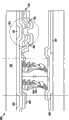
图1图示了低温多晶硅薄膜晶体管(LTPS TFT)显示器100的一个像素,所述低温多晶硅薄膜晶体管(LTPS TFT)显示器100包括反转的底部栅极结构,即,底部栅极结构被翻起使得栅极现在朝向外部。如上所简要描述的,栅极结构因此在显示器的顶部附近,并且也在显示器顶部附近的栅极驱动线被重新用于驱动激励。传感器信号针对驱动器被输入到装置控制器。为了如上所述的分路方法的激励和感测,可以向LTPS TFT添加硬件,使得在一个实施例中在每几个行和每几个列上作出模数转换(ADC)。ADC可以仅仅是在每几个行上或者每几个列上,或者两者都不是。FIG. 1 illustrates one pixel of a low temperature polysilicon thin film transistor (LTPS TFT)
电容性感测显示结构包括晶体管的矩阵,其一个晶体管102被图示在图1中。来自像素的光由背光灯产生,并且可以通过例如在胆甾醇液晶(CLC)物质104上的扭曲向列型晶体103,所述胆甾醇液晶(CLC)物质104耦接到公共电极106,并且耦接到像素电极108,并且光从可以是一块玻璃的顶部透明基底110出来。黑色矩阵层可以邻近透明基底110。黑色矩阵层可以例如是CrOx层,替换在底部栅极结构中使用的反射Cr层。在通常的黑色显示器中,黑色矩阵层可能不可见。可以例如是Cr层的反射层114与黑色矩阵层相对。反射层114位于底部栅极结构中替换在底部栅极结构中使用的黑色矩阵。栅极116和其源极118和漏极120以在显示装置领域中已知的方式工作。下面将更详细地讨论数据总线的线或者列驱动线122和栅极驱动(在此未示出)以及电容性存储电容器124。The capacitive sensing display structure includes a matrix of transistors, one
如下面将更详细描述的,通过所描述的底部栅极结构的重新布置和包括可能的最小附加硬件的修改使得它是反转的底部栅极结构,显示器的列线和行线基本上与作为触摸屏的表面的透明基底相邻。以这种方式,被配置成产生显示输出的多个列线和行线中的至少一个包括驱动器,该驱动器提供激励输出以产生与作为触摸屏装置的表面的顶部透明基底110的表面相邻的感应电场。而且,通过所描述的反转的底部栅极结构,被配置成产生显示输出的多个行线和列线中的至少一个包括耦接到传感器输出线的具有传感器输入的驱动器。感测线被配置成感测在与触摸屏装置的表面相邻的感应电场中是否有变化,并且经由至少一个传感器输出线向控制器(在下面示出)传送电容性感测信号。As will be described in more detail below, through the described rearrangement of the bottom gate structure and modifications including the minimum additional hardware possible so that it is an inverted bottom gate structure, the column and row lines of the display are essentially the same as The transparent substrate is adjacent to the surface of the touch screen. In this manner, at least one of the plurality of column and row lines configured to produce a display output includes a driver that provides an actuation output to produce sensing adjacent the surface of the top
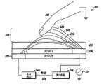
图2图示了显示装置200的一部分和诸如手指或者触针226的物体226。可以是透明的基底210的装置200表面与包括用于激励的列线230的印刷电路板(PCB)层1相邻,并且PCB层232耦接到感测线(参见图3)。列线230包括驱动器,该驱动器具有激励输出234以在表面310上或者上方产生感应电场236。如上所述,感测电容的分路方法使得,当手指或者某个其他接地物体226干扰电场236时,一些电场线——在这个示例中是电场线238、240和242——被分路到地,并且没有达到传感器线,诸如用作接收器的传感器线232。因此,当物体接近感应电场时,在接收器西格玛德耳塔模数转换器(∑-δ模数转换器)处测量的总的电容降低。在传感器线232处测量的电场线236被ADC 244转换到数字域中。ADC 244被图示为向显示装置的控制器246发送数据。与例如传感器线232的传感器输出线进行通信的控制器246被配置成接收电容性感测数据,并且确定物体已经进入感应电场中的位置。用于确定位置的计算可以基于哪个传感器线232经由它的传感器输出线248向控制器246传送电容性感测信号。FIG. 2 illustrates a portion of a
图3图示了TFT LCD显示矩阵350的一部分,TFT LCD显示矩阵350如上所述与显示装置的上表面相邻。由于另外的底部栅极结构被翻起以成为具有重新布置和包括附加硬件的修改的反转底部栅极结构,因此列线和行线与顶部透明基底110相邻(参见图1),并且因此在触摸屏显示装置200的表面附近(参见图2)。在图3中,栅极驱动器和激励开关在列线上,并且感测线在交替的列线上。列线330、352和354用作感应电场的激励源,并且列线351、353和355用作具有耦接的传感器线372、373和374的传感器,以确定在表面附近的物体的位置。应当理解,虽然在图3中图示的列线用作激励源并且用作传感器,但是行线332、356、357、358和359可以用作激励源和感测线两者(如参考图4所讨论的)。此外,可以通过以任何适当布置的列线和行线两者来完成激励和感测两者。所描述的驱动器和感测线的布置可以除了其它之外取决于装置的其他组件和它们的安置的方便性。FIG. 3 illustrates a portion of a TFT LCD display matrix 350 adjacent to the upper surface of the display device as described above. Since the additional bottom gate structure is flipped to become a modified inverted bottom gate structure with rearrangement and including additional hardware, the column and row lines are adjacent to the top transparent substrate 110 (see FIG. Near the surface of the touch screen display device 200 (see FIG. 2 ). In Figure 3, the gate drivers and actuation switches are on column lines, and the sense lines are on alternating column lines.
所述行被图示为包括栅极驱动器361、362、363、364和365,每条线一个。所述列被图示为包括列驱动线366、367、368、369、370和371,它们可以是每个子像素一个。通常,一次以3的倍数(R,G和B)来发送子像素数据。因此,在图3中图示的矩阵不是通常的使用情况。感测线372、373和374可以向控制器246传送电容性感测信号数据(参见图2),以表征在感应电场中的变化,以基于至少一个电容性感测信号来确定物体在触摸屏装置附近的位置。The rows are shown to include
在图3的放大的泡中图示的列线和感测线的相交处375,如图1中图示的顶部结构TFT可以包括存储电容器312和与栅极驱动通信的CLC303,所述栅极驱动例如栅极驱动361和列驱动线355。栅极驱动器361可以根据例如方波376来驱动行。列驱动线371可以驱动在时间t上活动和不活动的列数据377,特别是因为显示器可以操作为光栅扫描。At the
用于感应包括电场线236的电场的激励信号378(参见图2)与通常的列频率相比较可以是高频。开关380、381和382被图示为分别耦接到列线330、352和354。用于处理激励信号378的开关可以例如是电容性耦合、二极管或者电切换。激励的耦接可以当列线330、352和354不活动时发生在它们之上,并且优选地提供隔离以便不将列数据耦接到相邻列上。The excitation signal 378 (see FIG. 2 ) used to induce the electric field including the
图4图示了另一个实施例,其中,栅极驱动器460、461、462和463分别被交织在交替的行线432、456、457和458上,并且激励开关480和481在奇数行线上,并且感测线484和485在偶数行线上。在本讨论和图5的讨论中行线432、456、457和458分别被称为行n、行n+1、行n+2和行n+3。应当理解,诸如开关480和481和感测线372、373和374的组件的位置(参见图3)可以相对于列线和行线矩阵处于任何适当位置并且可以以任何适当的比率。如在图3中那样,图4示出了列线430、451、452和453和列驱动线466、467、468和469。如参考图3所述,诸如线466的列驱动线可以驱动在时间t上活动和不活动的列显示数据377。Figure 4 illustrates another embodiment in which gate drivers 460, 461, 462, and 463 are interleaved on alternating row lines 432, 456, 457, and 458, respectively, and drive switches 480 and 481 are on odd row lines , and the sensing lines 484 and 485 are on even row lines. Row lines 432, 456, 457, and 458 are referred to as row n, row n+1, row n+2, and row n+3, respectively, in this discussion and in the discussion of FIG. It should be understood that the locations of components such as switches 480 and 481 and
图5是针对接收到的分路检测的显示器和激励输出的时序图。图5图示了行n在行n+1的休眠时段期间激励行n+1。行n+2也可以激励感测行n+1。这对于行n+3也是成立的。在行线532上图示的波形586包括与列频率相比较高频的同一类型的激励信号378(参见图3)。在这个示例中,与行线通信的控制器246(参见图2)进一步被配置成使得行线532交替地产生时变的感应电场和显示输出。即,当显示信号关闭时,激励信号接通。当显示器信号关闭时,与具有激励输出的开关480通信的驱动器460(参见图4)通过小幅度和高频的激励来引起时变感应电场。Figure 5 is a timing diagram of the display and stimulus output for a received shunt detection. Figure 5 illustrates row n energizing row n+1 during a sleep period for
行n+1图示了与激励波形586交替的如上所述的行556的显示波形587。箭头588指示在这个示例中在激励波形586下图示了分路电荷589,两者同时发生。如上所述,当手指226或者其他物体干扰电场236时并且一些或者全部电场线被分路到地并且没有达到接收器时,分路电荷589可以如图2中所示发生。箭头590指示在这个示例中在行557的激励波形592上图示了分路电荷591,两者同时发生。类似地,箭头593指示在这个示例中在激励波形592下图示了分路电荷594,两者同时发生。在作为行n+3的行线558上,图示了显示波形595和另一个分路电荷596。应当理解,与这个示例相比较,行线和列线的矩阵可以很大。例如,可以以在所描述的触摸屏显示器上用一个手指覆盖20-30行。尖的触针可以仅仅覆盖一行。Row n+1 illustrates the
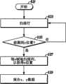
图6图示了触摸感测算法,其中,感测线可以在例如x方向的一个方向上并且然后在另一个方向y方向上扫描。根据用于确定在触摸屏上的物体的位置的算法,扫描可以不必包括在x方向上的扫描。如参考图5所述,为了开始621,如波形587和595所示来产生显示输出(参见图5)。在与当产生显示输出的时间不同的时间在触摸屏装置236(参见图2)的表面上产生感应电场。如上所述,在激励中的偏差可以确定从所产生的电场接收的电场线的德耳塔(德耳塔是第一值和第二值之差的数学标记)。在偶数线上的感测——在这种情况下是行n+1和行n+3——使用列驱动计数以确定x位置。因此,在这个示例中,行被扫描623,以检测625y方向物体位置。如果没有物体被检测为具有y方向位置,则扫描623继续。如果物体被检测为具有y方向位置,则对于在光栅扫描中的一些或者每个帧进行列扫描627,以获得x方向物体位置。为了避免在显示屏幕中的闪烁,列扫描627可以是每隔一个帧或者更多。用于表示电容性感测信号的x方向和y方向数据的数据被传送629到控制器246,使得它可以表征在感应电场中的变化,以基于至少一个电容性感测信号来确定物体在触摸屏装置的表面附近的位置。Figure 6 illustrates a touch sensing algorithm, where a sense line can be scanned in one direction, eg x-direction, and then in another direction, y-direction. Depending on the algorithm used to determine the position of the object on the touch screen, scanning may not necessarily include scanning in the x-direction. As described with reference to FIG. 5, to begin 621, a display output is generated as shown by
由于如上所述的列线和行线与以触摸屏显示器的表面为表面的透明基底相邻,如上所述的触摸屏显示器被实现在玻璃层之间,并且因此可以独立于玻璃厚度。由于装置——特别是移动通信装置——已经变得越来越小和越来越薄,因此所描述的触摸屏可以与许多形式的因素兼容。而且,特别是所描述的薄设计触摸屏可以避免降低显示亮度。所描述的触摸屏也有益地重新使用已经作为装置的一部分的组件。在上述触摸屏中,翻起底部栅极结构以用最少的附加硬件或者软件组件成为反转的底部栅极结构,使得基本上增加装置大小和/或复杂性,也可以提供成本效益。Since the column and row lines as described above are adjacent to the transparent substrate surfaced at the surface of the touch screen display, the touch screen display as described above is realized between glass layers and thus can be independent of glass thickness. As devices, especially mobile communication devices, have become smaller and thinner, the described touch screens are compatible with many form factors. Furthermore, especially the described thin design of the touchscreen avoids a reduction in display brightness. The described touch screen also advantageously reuses components that are already part of the device. In the touch screens described above, flipping the bottom gate structure to become an inverted bottom gate structure with minimal additional hardware or software components, resulting in substantially increased device size and/or complexity, may also provide cost benefits.
本公开意在解释如何形成和使用根据该技术的各个实施例,而不是限定其真实的、希望的和公平的范围和精神。上述说明不意在是穷尽性的,或者限制成所公开的确切形式。鉴于以上教导可以进行修改或者改变。选择和描述实施例(多个)以提供所描述的技术及其实践应用的原理的最佳说明,并且使得本领域内的普通技术人员能够使用在各个实施例中的技术并且各种修改适合于预期的特定用途。当根据所有这样的修改和改变被公平地、合法地和公正地授权的宽度来解释时,所有这样的修改和改变在由权利要求及其所有等同物确定的本发明的范围中,所述权利要求可以在本申请的未决期间被修改。This disclosure is intended to explain how to make and use various embodiments in accordance with the technology rather than to limit the true, intended, and fair scope and spirit thereof. The above description is not intended to be exhaustive or to be limited to the precise form disclosed. Modifications or variations are possible in light of the above teachings. The embodiment(s) were chosen and described in order to provide the best illustration of the principles of the described techniques and their practical applications, and to enable one of ordinary skill in the art to use the techniques in the various embodiments with various modifications as appropriate intended specific use. All such modifications and changes are within the scope of the invention as determined by the claims and all their equivalents when interpreted in accordance with the breadth to which they are fairly, legally and equitably entitled, said Requirements may be amended during the pendency of this application.
Claims (20)
Applications Claiming Priority (3)
| Application Number | Priority Date | Filing Date | Title |
|---|---|---|---|
| US11/859,997 | 2007-09-24 | ||
| US11/859,997US20090079707A1 (en) | 2007-09-24 | 2007-09-24 | Integrated capacitive sensing devices and methods |
| PCT/US2008/076137WO2009042422A2 (en) | 2007-09-24 | 2008-09-12 | Integrated capacitive sensing devices and methods |
Publications (1)
| Publication Number | Publication Date |
|---|---|
| CN101809530Atrue CN101809530A (en) | 2010-08-18 |
Family
ID=40471090
Family Applications (1)
| Application Number | Title | Priority Date | Filing Date |
|---|---|---|---|
| CN200880108329APendingCN101809530A (en) | 2007-09-24 | 2008-09-12 | Integrated capacitive sensing apparatus and method |
Country Status (8)
| Country | Link |
|---|---|
| US (1) | US20090079707A1 (en) |
| EP (1) | EP2193428A2 (en) |
| KR (1) | KR20100046270A (en) |
| CN (1) | CN101809530A (en) |
| BR (1) | BRPI0817980A2 (en) |
| MX (1) | MX2010003237A (en) |
| RU (1) | RU2010116164A (en) |
| WO (1) | WO2009042422A2 (en) |
Cited By (2)
| Publication number | Priority date | Publication date | Assignee | Title |
|---|---|---|---|---|
| CN103918182A (en)* | 2011-10-21 | 2014-07-09 | 微晶片科技德国第二公司 | Electrode arrangement of a capacitive sensor arrangement for position detection |
| CN105302397A (en)* | 2014-06-27 | 2016-02-03 | 辛纳普蒂克斯公司 | Interleaved capacitive sensing |
Families Citing this family (30)
| Publication number | Priority date | Publication date | Assignee | Title |
|---|---|---|---|---|
| TW200947030A (en)* | 2008-05-13 | 2009-11-16 | Tpk Touch Solutions Inc | Capacitive touch control device and method thereof |
| US9477342B2 (en) | 2008-08-26 | 2016-10-25 | Google Technology Holdings LLC | Multi-touch force sensing touch-screen devices and methods |
| US8643624B2 (en)* | 2009-03-18 | 2014-02-04 | Synaptics Incorporated | Capacitive sensing using a segmented common voltage electrode of a display |
| KR101610109B1 (en) | 2009-05-19 | 2016-04-11 | 삼성전자주식회사 | Method and Apparatus for tracking input position using E-Field Communication |
| US20110007019A1 (en)* | 2009-07-07 | 2011-01-13 | Nuvoton Technology Corporation | Systems and methods for using tft-based lcd panels as capacitive touch sensors |
| TWI428661B (en)* | 2009-11-09 | 2014-03-01 | Silicon Integrated Sys Corp | Touch display apparatus |
| CN102884496B (en)* | 2010-02-26 | 2017-06-30 | 辛纳普蒂克斯公司 | Modify demodulation to avoid interference |
| CN102193693B (en)* | 2010-03-17 | 2014-03-19 | 群康科技(深圳)有限公司 | Touch panel and differential identification method thereof |
| US9898121B2 (en) | 2010-04-30 | 2018-02-20 | Synaptics Incorporated | Integrated capacitive sensing and displaying |
| KR20130016980A (en)* | 2011-08-09 | 2013-02-19 | 삼성디스플레이 주식회사 | Display device |
| JP5925896B2 (en)* | 2011-09-07 | 2016-05-25 | シナプティクス インコーポレイテッド | Capacitive detection during hidden update time |
| CN104380312B (en)* | 2012-02-06 | 2018-07-10 | 高通股份有限公司 | Use the system and method for electric field arrangement |
| US20130207899A1 (en)* | 2012-02-09 | 2013-08-15 | Po-Hsien Wang | Touch-sensing display device |
| KR101971147B1 (en) | 2012-04-09 | 2019-04-23 | 삼성디스플레이 주식회사 | Display device including touch sensor |
| KR101929427B1 (en) | 2012-06-14 | 2018-12-17 | 삼성디스플레이 주식회사 | Display device including touch sensor |
| JP2014021799A (en)* | 2012-07-20 | 2014-02-03 | Kyocera Display Corp | Touch panel device |
| US10073568B2 (en) | 2012-08-15 | 2018-09-11 | Synaptics Incorporated | System and method for interference avoidance for a display device comprising an integrated sensing device |
| CN102866815B (en)* | 2012-09-03 | 2015-07-01 | 北京京东方光电科技有限公司 | Capacitance type embedded touch screen and display device |
| CN103293785B (en)* | 2012-12-24 | 2016-05-18 | 上海天马微电子有限公司 | TN (twisted nematic) type liquid crystal display device and touch control method thereof |
| US9235299B2 (en) | 2013-02-06 | 2016-01-12 | Google Technology Holdings LLC | Touch sensitive surface for an electronic device with false touch protection |
| JP2014174851A (en)* | 2013-03-11 | 2014-09-22 | Japan Display Inc | Touch sensor device, display device and electronic device |
| CN103699282B (en)* | 2013-12-24 | 2016-12-07 | 华映视讯(吴江)有限公司 | Touch control display apparatus |
| US9582099B2 (en) | 2014-03-31 | 2017-02-28 | Synaptics Incorporated | Serrated input sensing intervals |
| CN106796467A (en)* | 2014-10-07 | 2017-05-31 | 美国亚德诺半导体公司 | The capacitance sensing of aggregation |
| US10175827B2 (en) | 2014-12-23 | 2019-01-08 | Synaptics Incorporated | Detecting an active pen using a capacitive sensing device |
| US10394391B2 (en) | 2015-01-05 | 2019-08-27 | Synaptics Incorporated | System and method for reducing display artifacts |
| US10275070B2 (en) | 2015-01-05 | 2019-04-30 | Synaptics Incorporated | Time sharing of display and sensing data |
| CN105183252B (en)* | 2015-08-13 | 2016-11-02 | 京东方科技集团股份有限公司 | An array substrate, a touch display screen, a display device, and a driving method |
| US10037112B2 (en) | 2015-09-30 | 2018-07-31 | Synaptics Incorporated | Sensing an active device'S transmission using timing interleaved with display updates |
| US10592022B2 (en) | 2015-12-29 | 2020-03-17 | Synaptics Incorporated | Display device with an integrated sensing device having multiple gate driver circuits |
Family Cites Families (8)
| Publication number | Priority date | Publication date | Assignee | Title |
|---|---|---|---|---|
| US5543590A (en)* | 1992-06-08 | 1996-08-06 | Synaptics, Incorporated | Object position detector with edge motion feature |
| US5847690A (en)* | 1995-10-24 | 1998-12-08 | Lucent Technologies Inc. | Integrated liquid crystal display and digitizer having a black matrix layer adapted for sensing screen touch location |
| US5777596A (en)* | 1995-11-13 | 1998-07-07 | Symbios, Inc. | Touch sensitive flat panel display |
| US6274887B1 (en)* | 1998-11-02 | 2001-08-14 | Semiconductor Energy Laboratory Co., Ltd. | Semiconductor device and manufacturing method therefor |
| GB0114456D0 (en)* | 2001-06-14 | 2001-08-08 | Koninkl Philips Electronics Nv | Object sensing |
| TWI245252B (en)* | 2002-07-18 | 2005-12-11 | Gigno Technology Co Ltd | LCD and the touch-control method thereof |
| JP2005322160A (en)* | 2004-05-11 | 2005-11-17 | Olympus Corp | Display device with touch panel |
| GB0412787D0 (en)* | 2004-06-09 | 2004-07-14 | Koninkl Philips Electronics Nv | Input system |
- 2007
- 2007-09-24USUS11/859,997patent/US20090079707A1/ennot_activeAbandoned
- 2008
- 2008-09-12EPEP08834247Apatent/EP2193428A2/ennot_activeWithdrawn
- 2008-09-12KRKR1020107006446Apatent/KR20100046270A/ennot_activeCeased
- 2008-09-12WOPCT/US2008/076137patent/WO2009042422A2/enactiveApplication Filing
- 2008-09-12CNCN200880108329Apatent/CN101809530A/enactivePending
- 2008-09-12MXMX2010003237Apatent/MX2010003237A/enunknown
- 2008-09-12RURU2010116164/08Apatent/RU2010116164A/enunknown
- 2008-09-12BRBRPI0817980patent/BRPI0817980A2/ennot_activeApplication Discontinuation
Cited By (4)
| Publication number | Priority date | Publication date | Assignee | Title |
|---|---|---|---|---|
| CN103918182A (en)* | 2011-10-21 | 2014-07-09 | 微晶片科技德国第二公司 | Electrode arrangement of a capacitive sensor arrangement for position detection |
| CN103918182B (en)* | 2011-10-21 | 2018-02-06 | 微晶片科技德国公司 | Electrode arrangement of a capacitive sensor arrangement for position detection |
| CN105302397A (en)* | 2014-06-27 | 2016-02-03 | 辛纳普蒂克斯公司 | Interleaved capacitive sensing |
| CN105302397B (en)* | 2014-06-27 | 2019-07-12 | 辛纳普蒂克斯公司 | Sensor electrode is driven to carry out the method and device of capacitive sensing |
Also Published As
| Publication number | Publication date |
|---|---|
| WO2009042422A2 (en) | 2009-04-02 |
| US20090079707A1 (en) | 2009-03-26 |
| KR20100046270A (en) | 2010-05-06 |
| BRPI0817980A2 (en) | 2015-04-07 |
| WO2009042422A3 (en) | 2009-06-04 |
| MX2010003237A (en) | 2010-04-21 |
| EP2193428A2 (en) | 2010-06-09 |
| RU2010116164A (en) | 2011-11-10 |
Similar Documents
| Publication | Publication Date | Title |
|---|---|---|
| CN101809530A (en) | Integrated capacitive sensing apparatus and method | |
| CN103926729B (en) | Array substrate, color film substrate, touch display device and driving method thereof | |
| US9262024B2 (en) | Liquid crystal display panel including touch sensor and liquid crystal display using the same | |
| CN102446026B (en) | There is the display device of touch panel | |
| KR102319325B1 (en) | Touch screen liquid crystal display | |
| CN103135815B (en) | Liquid crystal display device with embedded touch screen and touch control driving method thereof | |
| US9229590B2 (en) | Display device | |
| KR101062042B1 (en) | Touch screen liquid crystal display | |
| US20120169635A1 (en) | Touchable sensing matrix unit, a co-constructed active array substrate having the touchable sensing matrix unit and a display having the co-constructed active array substrate | |
| US9753589B2 (en) | Touch sensing system | |
| US9690420B2 (en) | Display device having touch sensor | |
| CN101311890A (en) | Double-sided touch sensitive panel with protective layer and combined drive layer | |
| CN103412673B (en) | Colored film substrate, manufacturing method of colored film substrate and touch screen | |
| KR101862397B1 (en) | Touch sensor integrated type display | |
| TWI763740B (en) | Touch sensor signal integration | |
| CN105204700A (en) | Touch display panel | |
| KR20120054451A (en) | Touch screen, and driving method thereof, and display device including the touch screen | |
| KR20120055175A (en) | Apparatus and method for driving touch sensor | |
| KR101810223B1 (en) | Display device comprising touch screen panel | |
| AU2017200964B2 (en) | Touch screen liquid crystal display | |
| CN116339538A (en) | Touch display device |
Legal Events
| Date | Code | Title | Description |
|---|---|---|---|
| C06 | Publication | ||
| PB01 | Publication | ||
| C10 | Entry into substantive examination | ||
| SE01 | Entry into force of request for substantive examination | ||
| ASS | Succession or assignment of patent right | Owner name:MOTOROLA MOBILE CO., LTD. Free format text:FORMER OWNER: MOTOROLA INC. Effective date:20110113 | |
| C41 | Transfer of patent application or patent right or utility model | ||
| TA01 | Transfer of patent application right | Effective date of registration:20110113 Address after:Illinois State Applicant after:Motorola Mobility LLC Address before:Illinois State Applicant before:Motorola Inc. | |
| C02 | Deemed withdrawal of patent application after publication (patent law 2001) | ||
| WD01 | Invention patent application deemed withdrawn after publication | Application publication date:20100818 |