CN101802948B - Tandem photovoltaic cells - Google Patents
Tandem photovoltaic cellsDownload PDFInfo
- Publication number
- CN101802948B CN101802948BCN200880108241.0ACN200880108241ACN101802948BCN 101802948 BCN101802948 BCN 101802948BCN 200880108241 ACN200880108241 ACN 200880108241ACN 101802948 BCN101802948 BCN 101802948B
- Authority
- CN
- China
- Prior art keywords
- photovoltaic element
- solar cell
- dye
- layer
- electrode
- Prior art date
- Legal status (The legal status is an assumption and is not a legal conclusion. Google has not performed a legal analysis and makes no representation as to the accuracy of the status listed.)
- Expired - Fee Related
Links
Images


Classifications
- H—ELECTRICITY
- H01—ELECTRIC ELEMENTS
- H01G—CAPACITORS; CAPACITORS, RECTIFIERS, DETECTORS, SWITCHING DEVICES, LIGHT-SENSITIVE OR TEMPERATURE-SENSITIVE DEVICES OF THE ELECTROLYTIC TYPE
- H01G9/00—Electrolytic capacitors, rectifiers, detectors, switching devices, light-sensitive or temperature-sensitive devices; Processes of their manufacture
- H01G9/20—Light-sensitive devices
- H01G9/2068—Panels or arrays of photoelectrochemical cells, e.g. photovoltaic modules based on photoelectrochemical cells
- H01G9/2072—Panels or arrays of photoelectrochemical cells, e.g. photovoltaic modules based on photoelectrochemical cells comprising two or more photoelectrodes sensible to different parts of the solar spectrum, e.g. tandem cells
- B—PERFORMING OPERATIONS; TRANSPORTING
- B82—NANOTECHNOLOGY
- B82Y—SPECIFIC USES OR APPLICATIONS OF NANOSTRUCTURES; MEASUREMENT OR ANALYSIS OF NANOSTRUCTURES; MANUFACTURE OR TREATMENT OF NANOSTRUCTURES
- B82Y10/00—Nanotechnology for information processing, storage or transmission, e.g. quantum computing or single electron logic
- H—ELECTRICITY
- H10—SEMICONDUCTOR DEVICES; ELECTRIC SOLID-STATE DEVICES NOT OTHERWISE PROVIDED FOR
- H10K—ORGANIC ELECTRIC SOLID-STATE DEVICES
- H10K30/00—Organic devices sensitive to infrared radiation, light, electromagnetic radiation of shorter wavelength or corpuscular radiation
- H10K30/10—Organic devices sensitive to infrared radiation, light, electromagnetic radiation of shorter wavelength or corpuscular radiation comprising heterojunctions between organic semiconductors and inorganic semiconductors
- H10K30/15—Sensitised wide-bandgap semiconductor devices, e.g. dye-sensitised TiO2
- H10K30/151—Sensitised wide-bandgap semiconductor devices, e.g. dye-sensitised TiO2 the wide bandgap semiconductor comprising titanium oxide, e.g. TiO2
- H—ELECTRICITY
- H10—SEMICONDUCTOR DEVICES; ELECTRIC SOLID-STATE DEVICES NOT OTHERWISE PROVIDED FOR
- H10K—ORGANIC ELECTRIC SOLID-STATE DEVICES
- H10K30/00—Organic devices sensitive to infrared radiation, light, electromagnetic radiation of shorter wavelength or corpuscular radiation
- H10K30/20—Organic devices sensitive to infrared radiation, light, electromagnetic radiation of shorter wavelength or corpuscular radiation comprising organic-organic junctions, e.g. donor-acceptor junctions
- H—ELECTRICITY
- H10—SEMICONDUCTOR DEVICES; ELECTRIC SOLID-STATE DEVICES NOT OTHERWISE PROVIDED FOR
- H10K—ORGANIC ELECTRIC SOLID-STATE DEVICES
- H10K30/00—Organic devices sensitive to infrared radiation, light, electromagnetic radiation of shorter wavelength or corpuscular radiation
- H10K30/50—Photovoltaic [PV] devices
- H10K30/57—Photovoltaic [PV] devices comprising multiple junctions, e.g. tandem PV cells
- H—ELECTRICITY
- H01—ELECTRIC ELEMENTS
- H01G—CAPACITORS; CAPACITORS, RECTIFIERS, DETECTORS, SWITCHING DEVICES, LIGHT-SENSITIVE OR TEMPERATURE-SENSITIVE DEVICES OF THE ELECTROLYTIC TYPE
- H01G9/00—Electrolytic capacitors, rectifiers, detectors, switching devices, light-sensitive or temperature-sensitive devices; Processes of their manufacture
- H01G9/20—Light-sensitive devices
- H01G9/2004—Light-sensitive devices characterised by the electrolyte, e.g. comprising an organic electrolyte
- H01G9/2009—Solid electrolytes
- H—ELECTRICITY
- H10—SEMICONDUCTOR DEVICES; ELECTRIC SOLID-STATE DEVICES NOT OTHERWISE PROVIDED FOR
- H10K—ORGANIC ELECTRIC SOLID-STATE DEVICES
- H10K85/00—Organic materials used in the body or electrodes of devices covered by this subclass
- H10K85/10—Organic polymers or oligomers
- H10K85/111—Organic polymers or oligomers comprising aromatic, heteroaromatic, or aryl chains, e.g. polyaniline, polyphenylene or polyphenylene vinylene
- H10K85/113—Heteroaromatic compounds comprising sulfur or selene, e.g. polythiophene
- H10K85/1135—Polyethylene dioxythiophene [PEDOT]; Derivatives thereof
- H—ELECTRICITY
- H10—SEMICONDUCTOR DEVICES; ELECTRIC SOLID-STATE DEVICES NOT OTHERWISE PROVIDED FOR
- H10K—ORGANIC ELECTRIC SOLID-STATE DEVICES
- H10K85/00—Organic materials used in the body or electrodes of devices covered by this subclass
- H10K85/20—Carbon compounds, e.g. carbon nanotubes or fullerenes
- H10K85/211—Fullerenes, e.g. C60
- H10K85/215—Fullerenes, e.g. C60 comprising substituents, e.g. PCBM
- H—ELECTRICITY
- H10—SEMICONDUCTOR DEVICES; ELECTRIC SOLID-STATE DEVICES NOT OTHERWISE PROVIDED FOR
- H10K—ORGANIC ELECTRIC SOLID-STATE DEVICES
- H10K85/00—Organic materials used in the body or electrodes of devices covered by this subclass
- H10K85/60—Organic compounds having low molecular weight
- H10K85/615—Polycyclic condensed aromatic hydrocarbons, e.g. anthracene
- H10K85/621—Aromatic anhydride or imide compounds, e.g. perylene tetra-carboxylic dianhydride or perylene tetracarboxylic di-imide
- Y—GENERAL TAGGING OF NEW TECHNOLOGICAL DEVELOPMENTS; GENERAL TAGGING OF CROSS-SECTIONAL TECHNOLOGIES SPANNING OVER SEVERAL SECTIONS OF THE IPC; TECHNICAL SUBJECTS COVERED BY FORMER USPC CROSS-REFERENCE ART COLLECTIONS [XRACs] AND DIGESTS
- Y02—TECHNOLOGIES OR APPLICATIONS FOR MITIGATION OR ADAPTATION AGAINST CLIMATE CHANGE
- Y02E—REDUCTION OF GREENHOUSE GAS [GHG] EMISSIONS, RELATED TO ENERGY GENERATION, TRANSMISSION OR DISTRIBUTION
- Y02E10/00—Energy generation through renewable energy sources
- Y02E10/50—Photovoltaic [PV] energy
- Y02E10/542—Dye sensitized solar cells
- Y—GENERAL TAGGING OF NEW TECHNOLOGICAL DEVELOPMENTS; GENERAL TAGGING OF CROSS-SECTIONAL TECHNOLOGIES SPANNING OVER SEVERAL SECTIONS OF THE IPC; TECHNICAL SUBJECTS COVERED BY FORMER USPC CROSS-REFERENCE ART COLLECTIONS [XRACs] AND DIGESTS
- Y02—TECHNOLOGIES OR APPLICATIONS FOR MITIGATION OR ADAPTATION AGAINST CLIMATE CHANGE
- Y02E—REDUCTION OF GREENHOUSE GAS [GHG] EMISSIONS, RELATED TO ENERGY GENERATION, TRANSMISSION OR DISTRIBUTION
- Y02E10/00—Energy generation through renewable energy sources
- Y02E10/50—Photovoltaic [PV] energy
- Y02E10/549—Organic PV cells
- Y—GENERAL TAGGING OF NEW TECHNOLOGICAL DEVELOPMENTS; GENERAL TAGGING OF CROSS-SECTIONAL TECHNOLOGIES SPANNING OVER SEVERAL SECTIONS OF THE IPC; TECHNICAL SUBJECTS COVERED BY FORMER USPC CROSS-REFERENCE ART COLLECTIONS [XRACs] AND DIGESTS
- Y02—TECHNOLOGIES OR APPLICATIONS FOR MITIGATION OR ADAPTATION AGAINST CLIMATE CHANGE
- Y02P—CLIMATE CHANGE MITIGATION TECHNOLOGIES IN THE PRODUCTION OR PROCESSING OF GOODS
- Y02P70/00—Climate change mitigation technologies in the production process for final industrial or consumer products
- Y02P70/50—Manufacturing or production processes characterised by the final manufactured product
Landscapes
- Engineering & Computer Science (AREA)
- Chemical & Material Sciences (AREA)
- Physics & Mathematics (AREA)
- Nanotechnology (AREA)
- Power Engineering (AREA)
- Electromagnetism (AREA)
- Microelectronics & Electronic Packaging (AREA)
- Electrochemistry (AREA)
- Sustainable Development (AREA)
- Mathematical Physics (AREA)
- Theoretical Computer Science (AREA)
- Crystallography & Structural Chemistry (AREA)
- Life Sciences & Earth Sciences (AREA)
- Chemical Kinetics & Catalysis (AREA)
- Inorganic Chemistry (AREA)
- Photovoltaic Devices (AREA)
- Hybrid Cells (AREA)
Abstract
Description
Translated fromChinese技术领域technical field
本发明涉及根据权利要求1的前序部分的具有串列电池结构的光伏元件。这样的光伏元件用于将电磁辐射,特别地太阳光,转换为电能。The invention relates to a photovoltaic element with a tandem cell structure according to the preamble of
背景技术Background technique
太阳能电池中的太阳能到电能的直接转换通常基于半导体材料的所谓的“内部光电效应”,即,通过在p-n结或肖特基(Schottky)接触处吸收光子并分离正负电荷载流子来产生电子空穴对。由此,产生光电压,该光电压在外部电路中可以诱导光电流,太阳能电池通过光电流输出其电力。The direct conversion of solar energy to electricity in solar cells is generally based on the so-called "internal photoelectric effect" of semiconductor materials, i.e., by absorbing photons and separating positive and negative charge carriers at p-n junctions or Schottky contacts electron-hole pairs. Thereby, a photovoltage is generated, which can induce a photocurrent in an external circuit, and the solar cell outputs its electric power through the photocurrent.
通常在该情况下,半导体仅吸收具有高于半导体带隙的能量的那些光子。因此,半导体带隙的大小决定了太阳光的可以被转换为电能的部分。Typically in this case the semiconductor absorbs only those photons with energies above the bandgap of the semiconductor. Thus, the size of the semiconductor bandgap determines the fraction of sunlight that can be converted into electricity.
在二十世纪五十年代就已经制造出了基于多晶硅的太阳能电池。在那时,为应用于太阳能卫星而推动了该技术。虽然现在基于硅的太阳能电池主宰着地面市场,但该技术仍然是成本高昂的。因此,尝试开发更经济的新方法。下面将概述作为本发明的基础的一些这样的方法。Solar cells based on polycrystalline silicon have been manufactured since the 1950s. At that time, the technology was promoted for application to solar-powered satellites. While silicon-based solar cells now dominate the terrestrial market, the technology remains cost-prohibitive. Therefore, try to develop new methods that are more economical. Some of these methods on which the present invention is based are outlined below.
染料太阳能电池dye solar cell
目前,染料太阳能电池(DSC)为最有效的备选太阳能技术。在该技术的液体变体(liquid variant)中,目前可以获得高达11%的效率(参见,例如,M.et al.,J.Photochem.Photobio.C,2003,4,145;Chiba etal.,Japanese Journal of Appl.Phys.,2006,45,L638-L640)。Currently, dye solar cells (DSCs) are the most efficient candidate solar technology. In the liquid variant of this technology, efficiencies of up to 11% are currently achievable (see, for example, M. et al., J. Photochem. Photobio. C, 2003, 4, 145; Chiba et al., Japanese Journal of Appl. Phys., 2006, 45, L638-L640).
其中具有许多变体的被构建为单个元件的太阳能电池通常包括两个电极,至少其中一个电极是透明的。这两个电极根据其功能被称为“工作电极”(或“阳极”,产生电子)和“背电极”(或“阴极”)。n型导电金属氧化物通常被施加在工作电极上或其附近,例如,约10-20μm厚度的二氧化钛(TiO2)的纳米多孔层。在该层的表面上进行吸收,通常存在可以通过光吸收而转变为受激态的光敏染料(例如,钌络合物)的单个层。通常在背电极上或背电极处存在几个微米厚的例如铂的催化层。在两个电极之间的区域填充有氧化还原电解质,例如,碘(I2)和碘化钾(KI)的溶液。Solar cells constructed as a single element, of which there are many variants, generally comprise two electrodes, at least one of which is transparent. These two electrodes are called "working electrode" (or "anode", which generates electrons) and "back electrode" (or "cathode") according to their functions. An n-type conducting metal oxide is typically applied on or near the working electrode, eg, a nanoporous layer of titanium dioxide (TiO2 ) of about 10-20 μm thickness. Absorption occurs on the surface of this layer, and there is usually a single layer of a sensitizing dye (eg, a ruthenium complex) that can be converted to an excited state by light absorption. Typically on or at the back electrode there is a catalytic layer of eg platinum several micrometers thick. The area between the two electrodes is filled with a redox electrolyte, eg a solution of iodine (I2 ) and potassium iodide (KI).
染料太阳能电池的功能是基于通过染料吸收光。电子从受激的染料转移到n型半导电金属氧化物半导体,并从那里迁移到阳极,而电解质通过阴极确保电荷平衡。因此,N型半导电金属氧化物、染料以及电介质是染料太阳能电池的基本元件。The function of dye solar cells is based on the absorption of light by dyes. Electrons are transferred from the excited dye to the n-type semiconducting metal oxide semiconductor and from there to the anode, while the electrolyte ensures charge balance through the cathode. Therefore, N-type semiconducting metal oxides, dyes, and dielectrics are the basic components of dye solar cells.
然而,在一些情况下,由液体电介质制成的染料太阳能电池会遭受不是最理想的密封,这会导致稳定性问题。然而,可用通过固体p型半导体取代液体电解质。目前染料太阳能电池的固体变体(solid variant)的效率为约4.6-4.7%(Snaith,H.,Angew.Chem.Int.Ed.,2005,44,6413-6417)。However, in some cases, dye solar cells made of liquid dielectrics suffer from suboptimal sealing, which leads to stability problems. However, the liquid electrolyte can be replaced by a solid p-type semiconductor. Current solid variants of dye solar cells have efficiencies of about 4.6-4.7% (Snaith, H., Angew. Chem. Int. Ed., 2005, 44, 6413-6417).
迄今为止,已经在固体染料太阳能电池中使用各种无机p型半导体,例如,CuI,CuBr·3(S(C4H9)2)或CuSCN。本质上,还存在Cu(I)酶质体蓝素(plastocyanine),其在光系统I中重新还原被氧化的叶绿素二聚体。这样的p型半导体可以通过至少三种方法处理,即,从溶液、通过电沉积或通过激光沉积。To date, various inorganic p-type semiconductors have been used in solid dye solar cells, for example CuI, CuBr·3(S(C4 H9 )2 ) or CuSCN. Essentially, there is also the Cu(I) enzyme plastocyanine, which in photosystem I re-reduces oxidized chlorophyll dimers. Such p-type semiconductors can be processed by at least three methods, namely, from solution, by electrodeposition or by laser deposition.
然而,在实践中,这有时会引起p型半导体的稳定性问题,这些问题具体地是由于过大的半导体晶体和与染料的差的接触导致的。避免此点的一种方法涉及在有机溶剂中的CuI溶液,其添加有离子液体作为结晶抑制剂。可以为此使用各种结晶抑制剂(通常为SCN盐),并且可以获得高达3.75%的效率。另一组使用被ZnO覆盖的纳米多孔TiO2层,并结合CuI和1-甲基-3乙基咪唑鎓硫氰酸盐(MEISCN)。这些染料太阳能电池呈现3.8%的效率。当与氢硫氰酸三乙胺(triethyl amine hydrothiocyanate)(作为结晶抑制剂)一起使用MgO覆盖的TiO2和CuI(作为p型导体)时,获得高达4.7%的效率。来自溶液的CuSCN还可以用作固体p型半导体并呈现约2%的效率。如果可以在负电势下沉积p型半导体,电化学沉积应允许更好地渗透到介孔(mesoporous)型孔中。利用该方法,虽然通常由于相对薄的ZnO层而仅仅吸收了仅仅约12%的入射光,但固体染料太阳能电池输出1.5%的效率。最后,通过激光沉积制造相对小的晶粒,这导致非常良好的约12.2mA/cm2的短路电流ISC,尽管约10微米厚度的TiO2层,并且对于约1cm2的活性表面面积的效率为约2.8%。However, in practice this sometimes causes stability problems of the p-type semiconductor, in particular due to overly large semiconductor crystals and poor contact with the dye. One way to avoid this involves solutions of CuI in organic solvents with the addition of ionic liquids as crystallization inhibitors. Various crystallization inhibitors (usually SCN salts) can be used for this and efficiencies as high as 3.75% can be achieved. Another group used nanoporousTiO2 layers covered by ZnO, combined with CuI and 1-methyl-3 ethylimidazolium thiocyanate (MEISCN). These dye solar cells exhibited an efficiency of 3.8%. Efficiencies as high as 4.7% were obtained when MgO-coveredTiO2 and CuI (as p-type conductor) were used together with triethylamine hydrothiocyanate (as crystallization inhibitor). CuSCN from solution can also be used as a solid p-type semiconductor and exhibits an efficiency of about 2%. If p-type semiconductors can be deposited at negative potentials, electrochemical deposition should allow better penetration into mesoporous type pores. Using this approach, solid dye solar cells output efficiencies of 1.5%, although typically only about 12% of incident light is absorbed due to the relatively thin ZnO layer. Finally, relatively small grains were fabricated by laser deposition, which resulted in a very good short-circuit currentISC of about 12.2 mA/cm2 despite aTiO2 layer of about 10 micron thickness, and an efficiency for an active surface area of about 1cm2 is about 2.8%.
有机聚合物也已经被用作固体p型半导体。其实例包括聚吡咯、聚(3,4-亚乙基二氧噻吩)、基于咔唑的聚合物、聚苯胺、聚(4-十一烷基-2,2’-二噻吩)、聚(3-辛基噻吩)、聚(三丙基二胺)以及聚(N-乙烯基咔唑)。在聚(N-乙烯基咔唑)的情况下,效率达到2%。原位聚合的PEDOT(聚(3,4-亚乙基二氧噻吩))也已显示出0.53%的效率。典型地不是以纯的形式使用这里描述的聚合物,而是具有添加剂。Organic polymers have also been used as solid p-type semiconductors. Examples include polypyrrole, poly(3,4-ethylenedioxythiophene), carbazole-based polymers, polyaniline, poly(4-undecyl-2,2'-dithiophene), poly( 3-octylthiophene), poly(tripropyldiamine), and poly(N-vinylcarbazole). In the case of poly(N-vinylcarbazole), the efficiency reaches 2%. In situ polymerized PEDOT (poly(3,4-ethylenedioxythiophene)) has also shown an efficiency of 0.53%. Typically the polymers described here are not used in pure form but with additives.
还可以采用低分子量的有机p型半导体。低分子量的有机p型半导体在固体染料太阳能电池中的首次使用是用三苯基胺(TPD)的气相沉积层取代液体电解质。在1998年报道了在染料太阳能电池中使用有机化合物2,2’7,7’-四(N,N-二对甲氧基苯基胺)-9,9’-螺二芴(螺-MeOTAD)。其可以从溶液引入并具有相对高的玻璃化温度,这防止了不希望的结晶和与染料的差接触。甲氧基调整螺-MeOTAD的氧化电势,以便Ru络合物可有效地再生。使用螺-MeOTAD自身作为p型导体已给出了5%的最大IPCE(入射光至电流转换效率)。当协同使用N(PhBr)3SbCl6(作为掺杂剂)和Li[(CF3SO2)2N]时,IPCE升高到33%,并且效率为0.74%。通过使用叔丁基吡啶作为固体p型半导体,可以将效率提高到2.56%,对于约1.07cm2的活性表面面积,开路电压(Voc)为约910mV且短路电流Isc为约5mA(参见,Krüger et al.,Appl.Phys.Lett.,2001,79,2085)。可以实现TiO2层的较好覆盖并在螺-MeOTAD上具有良好的润湿性的染料呈现出大于4%的效率。当钌络合物具有氧乙烯(oxyethylene)侧链时,甚至报道了更高的效率(4.6%)。Low molecular weight organic p-type semiconductors can also be used. The first use of low-molecular-weight organic p-type semiconductors in solid-state dye solar cells was to replace the liquid electrolyte with a vapor-deposited layer of triphenylamine (TPD). In 1998, the use of the
Adv.Mater.17,pp.813-815(2005)提出了用于使用螺二芴作为非晶有机p型导体的染料太阳能电池的二氢吲哚染料。该有机染料具有的消光系数比钌络合物的消光系数高四倍,在固体染料太阳能电池中呈现高效率(太阳光情况下为4.1%)。Adv. Mater. 17, pp. 813-815 (2005) proposes indoline dyes for dye solar cells using spirobifluorenes as amorphous organic p-type conductors. This organic dye has an extinction coefficient four times higher than that of the ruthenium complex and exhibits high efficiency (4.1% in the case of sunlight) in solid dye solar cells.
此外还提出了这样的构思,其中将聚合的p型半导体直接接合到Ru染料(Peter,K.,Appl.Phys.A2004,79,65)。Furthermore, the concept has also been proposed where polymeric p-type semiconductors are directly bonded to Ru dyes (Peter, K., Appl. Phys. A2004, 79, 65).
Durrant et al.,Adv.Munc.Mater.2006,16,1832-1838描述了在许多情况下,光电流直接依赖于从氧化的染料到固体p型半导体的空穴渡越的产率。这依赖于两个因素:首先依赖于p型导体的向氧化物孔中渗透的程度,其次依赖于用于电荷转移的热力学驱动力(即,具体地,染料与p型导体之间的自由焓差ΔG)。Durrant et al., Adv. Munc. Mater. 2006, 16, 1832-1838 describe that in many cases the photocurrent is directly dependent on the yield of hole transitions from the oxidized dye to the solid p-type semiconductor. This depends on two factors: firstly on the degree of penetration of the p-type conductor into the oxide pores, and secondly on the thermodynamic driving force for charge transfer (i.e., specifically, the free enthalpy between the dye and the p-type conductor difference ΔG).
染料太阳能电池的一个缺点在于,染料可以使用的光的部分受到所使用的n型与p型导体的费米能量之间的能量差的限制。光电压同样受该差异的限制。此外,由于所需的电荷输运,染料太阳能电池通常必须被制造得相当薄(例如,1-2.5微米),从而对入射光的利用通常不是最优的。One disadvantage of dye solar cells is that the fraction of light available to the dye is limited by the energy difference between the Fermi energy of the n-type and p-type conductors used. Photovoltage is also limited by this difference. Furthermore, due to the required charge transport, dye solar cells typically have to be fabricated quite thin (eg, 1-2.5 microns), so that the utilization of incident light is often not optimal.
有机太阳能电池organic solar battery
其中一些或甚至所有的光活性材料为有机的基于p-n结的光伏元件已经为人所知了几乎50年(参见,例如Kearns,K,Calvin,M.,J.,Chem.Phys.1958,29,950-951)。这样的元件被设计为使其中至少一种半导体(n型半导体和/或p型半导体)吸收光子,所产生的激子被输运到p-n结,并且两种电荷中的一种或两种被从那里输运到电极。p-n junction-based photovoltaic elements in which some or even all of the photoactive material is organic have been known for almost 50 years (see, for example, Kearns, K, Calvin, M., J., Chem. Phys. 1958, 29, 950-951). Such an element is designed such that at least one of the semiconductors (n-type and/or p-type) absorbs photons, the resulting excitons are transported to the p-n junction, and one or both of the two charges are dissipated From there it is transported to the electrodes.
有机太阳能电池由低分子量化合物(下面也称为“低分子量电池”)、聚合物(下面也称为“聚合物电池”)、低聚物或这些材料中的几种或更多种的组合。有机太阳能电池通常包含受主材料以及至少一种施主材料,在受主材料中n型电荷输运(电子输运)占优势,因此受主材料表示n型半导体的有机类似物(organic analog),而在施主材料中p型电荷输运(空穴输运)占优势,因此施主材料表示p型半导体的有机类似物。替代地或附加地,还可以使用无机纳米颗粒作为受主(例如,参见Alivisatos A.,Science,2002,295,2425-2427)。Organic solar cells are composed of low molecular weight compounds (hereinafter also referred to as "low molecular weight cells"), polymers (hereinafter also referred to as "polymer cells"), oligomers, or a combination of several or more of these materials. An organic solar cell generally comprises an acceptor material in which n-type charge transport (electron transport) predominates, and at least one donor material, the acceptor material thus representing an organic analog of an n-type semiconductor, Whereas in donor materials p-type charge transport (hole transport) predominates, donor materials thus represent organic analogues of p-type semiconductors. Alternatively or additionally, it is also possible to use inorganic nanoparticles as acceptors (see, for example, Alivisatos A., Science, 2002, 295, 2425-2427).
为了说明的目的,根据处理方法对多种有机光伏概念进行分类。材料典型地在真空中(例如,通过物理气相沉积PVD、化学气相沉积CVD、分子束外延或其他方法或方法组合)施加和/或从溶液(例如,通过旋涂、印刷或其他湿法化学技术)沉积。还存在这些电池类型和沉积方法的混合,例如,具有在真空中施加的低分子量层和湿法化学施加的聚合层的电池。For illustrative purposes, the various organic photovoltaic concepts are categorized according to their approach. Materials are typically applied in vacuum (e.g., by physical vapor deposition PVD, chemical vapor deposition CVD, molecular beam epitaxy, or other methods or combinations of methods) and/or from solution (e.g., by spin-coating, printing, or other wet chemical techniques) ) deposition. There are also hybrids of these cell types and deposition methods, eg cells with low molecular weight layers applied in vacuum and polymeric layers applied wet chemically.
其中p型和n型材料都为真空沉积材料的低分子量电池已为人所知很多年(例如,参见Tang,C.W.,App.Phys.Lett.1986,48,183)。到目前为止,这些电池通常由作为施主材料的铜酞菁(CuPc)和作为受主材料的3,4,9,10-苝四羧酸双酰亚胺苯并咪唑(3,4,9,10-perylene tetracarboxylicacid bisimide benzimidazole)(PTCBI)或富勒烯(例如C60)。第一种Tang电池呈现约1%的效率。由相同有机材料制成的电池目前已被改善并达到2.7%的效率(Peumans et al.,Nature of Materials,2005,4,37-41)。Low molecular weight cells in which both p-type and n-type materials are vacuum deposited have been known for many years (see eg Tang, C.W., App. Phys. Lett. 1986, 48, 183). So far, these batteries are usually composed of copper phthalocyanine (CuPc) as the donor material and 3,4,9,10-perylenetetracarboxylic acid bisimide benzimidazole (3,4,9, 10-perylene tetracarboxylic acid bisimide benzimidazole) (PTCBI) or fullerene (eg C60). The first Tang cell exhibits an efficiency of about 1%. Cells made of the same organic material have now been improved and reached 2.7% efficiency (Peumans et al., Nature of Materials, 2005, 4, 37-41).
其中将C60用作受主材料的电池的效率目前已提高到5.0%。这可用以下两种方法实现:The efficiency of cells in which C60 is used as the acceptor material has so far been increased to 5.0%. This can be achieved in two ways:
在第一种方法中,替代光滑层结构,所谓的“体异质结”增加了n型与p型材料之间的界面。因此,增加的比例的激子被分离为自由空穴和自由电子,并可以产生电流。In the first approach, instead of a smooth layer structure, a so-called "bulk heterojunction" increases the interface between n-type and p-type materials. Therefore, an increased proportion of excitons is separated into free holes and free electrons, and electric current can be generated.
在第二种方法中,在受主层与阴极之间使用激子屏蔽层(EBL)。该层用于防止激子迁移到阴极,在阴极处激子会在金属与有机层之间的结处无用地衰减。此外,这些屏蔽层还作为扩散阻挡层以防止电极渗透到光活性材料中。In the second approach, an exciton shielding layer (EBL) is used between the acceptor layer and the cathode. This layer serves to prevent excitons from migrating to the cathode, where they would decay uselessly at the junction between the metal and organic layers. In addition, these shielding layers also act as diffusion barriers to prevent penetration of the electrodes into the photoactive material.
如果在Tang电池中用SubPc(亚酞菁)替代CuPc,则可以获得更高的光电压Voc(高达约0.97V,参见Mutolo,K.,J.Am.Chem.Soc.,2006,128,8108)。其他材料组合,例如,作为施主材料的低聚噻吩(oligiothiophene)(例如,α,α’-双(2,2-二氰基乙烯基)-五噻吩,DCV5T)与作为受主材料的C60的组合同样呈现高效率(例如,3.4-3.8%,参见Schulze et al.,Adv.Mater.,2006,18,2872-2875;Schulze et al.,Proc.of SPIE Vol.6192,61920C-1(2006))。更近期的工作使用所谓的“三重态(triplet)”吸收体,其呈现出长激子扩散长度(Yang,Y.Adv.Mater.,2005,17,2841)。If SubPc (subphthalocyanine) is used instead of CuPc in Tang cells, higher photovoltage Voc (up to about 0.97V, see Mutolo, K., J.Am.Chem.Soc., 2006, 128, 8108). Other material combinations, e.g., oligiothiophene (e.g., α,α'-bis(2,2-dicyanovinyl)-pentathiophene, DCV5T) as donor material andC60 as acceptor material The combination of also exhibits high efficiency (for example, 3.4-3.8%, see Schulze et al., Adv. Mater., 2006, 18, 2872-2875; Schulze et al., Proc. of SPIE Vol.6192, 61920C-1 ( 2006)). More recent work uses so-called "triplet" absorbers, which exhibit long exciton diffusion lengths (Yang, Y. Adv. Mater., 2005, 17, 2841).
使用施加低分子量物质的真空方法的备选方法为使用可溶性低分子量化合物,该可溶性低分子量化合物与聚合物或低聚物相似,可以同样通过湿法化学施加。以该方式制造的电池根据与上述低分子量电池相同的原理而起作用。在这种情况下,从一种或多种溶液和/或分散体处理p型和n型材料。该类型的多种分子已经被用于这样的电池中,但是到目前为止效率较低。通过对结(即,体异质结)的热处理(退火),可以实现效率的改善,因为这改善了分子排列。该效果在所使用的分子为热致液晶时变得特别显著(参见Schmidt-Mende,L. et al.,Science2001,293,1119-1122)。An alternative to the vacuum method of applying low molecular weight species is the use of soluble low molecular weight compounds which, like polymers or oligomers, can likewise be applied by wet chemistry. Batteries made in this way function according to the same principles as the low molecular weight batteries described above. In this case, p-type and n-type materials are processed from one or more solutions and/or dispersions. Various molecules of this type have been used in such batteries, but so far with low efficiencies. Improvements in efficiency can be achieved by thermal treatment (annealing) of the junction (ie, bulk heterojunction), as this improves the molecular alignment. This effect becomes particularly pronounced when the molecules used are thermotropic liquid crystals (see Schmidt-Mende, L. et al., Science 2001, 293, 1119-1122).
另一构思(concept)在于在分子中共价接合施主材料和受主材料。然而,到目前为止,以该方式构建的电池类型仅仅呈现相对低的效率(参见Maggini,M.,Chem.Commun.,2002,2028-2029)。Another concept is to covalently join the donor material and the acceptor material in the molecule. However, cell types constructed in this way have so far only exhibited relatively low efficiencies (cf. Maggini, M., Chem. Commun., 2002, 2028-2029).
聚合物电池根据与上述低分子量电池相同的原理起作用。其区别在于,两种吸收体中的至少一种(即,受主材料和/或施主材料)为聚合物,因而通常从溶液来处理。可以使用的聚合物的实例为聚(对苯乙烯)(PPV)的衍生物,其中,依赖于取代基,施主材料和受主材料二者都会遭遇(encounter)。用作施主材料的聚合物的典型实例为MEH-PPV(甲基己基取代的PPV),而氰基取代的PPV(CN-PPV)可以用作受主材料。以该方式构建的聚合物电池的效率在1%的范围内。目前呈现最佳性能的系统由作为施主材料的P3HT(聚(3-己基噻吩))和作为受主材料的PCBM([6,6]-苯基-C61-丁酸甲酯)。已知具有高达4.8%-5.0%的效率的太阳能电池。也可使用低带隙聚合物,其呈现出改善的与太阳光谱的吸收重叠。通过使用PCBM可以实现约3.2%的效率。有时还在该情况下使用光学间隔物,以使活性层中的光吸收最大化。App.Phys.Lett.2001,78,841表明,对效率的影响依赖于处理(例如,所使用的溶剂等)。为了改善所吸收的光子的分数,使用新的材料,例如,低带隙聚合物,例如,PCPDTBT(聚[2,6-(4,4-二(2-乙基己基)-4H-环戊二烯并[2,1-b;3,4-b’]-二噻吩)-alt-4,7-(2,1,3-苯并噻二唑)])以及C71-PCBM,其呈现高达5.5%的效率。还可以使用聚合物作为施主材料,其中使用苝系或无机纳米棒(nanorod)作为受主材料,在后一情况下效率高达1.7%。Polymer batteries function according to the same principle as the low molecular weight batteries described above. The difference is that at least one of the two absorbers (ie the acceptor material and/or the donor material) is a polymer and is thus usually processed from solution. Examples of polymers that can be used are derivatives of poly(p-styrene) (PPV) in which, depending on the substituents, both donor and acceptor materials are encountered. A typical example of a polymer used as a donor material is MEH-PPV (methylhexyl-substituted PPV), while cyano-substituted PPV (CN-PPV) can be used as an acceptor material. Polymer batteries built in this way have efficiencies in the 1% range. The system presenting the best performance so far consists of P3HT (poly(3-hexylthiophene)) as donor material and PCBM ([6,6]-phenyl-C61 -butyric acid methyl ester) as acceptor material. Solar cells with efficiencies as high as 4.8%-5.0% are known. Low bandgap polymers, which exhibit improved absorption overlap with the solar spectrum, can also be used. An efficiency of about 3.2% can be achieved by using PCBM. Optical spacers are also sometimes used in this case to maximize light absorption in the active layer. App. Phys. Lett. 2001, 78, 841 shows that the effect on efficiency is process dependent (eg solvent used etc.). In order to improve the fraction of photons absorbed, new materials are used, e.g., low-bandgap polymers, e.g., PCPDTBT (poly[2,6-(4,4-bis(2-ethylhexyl)-4H-cyclopentyl) Dieno[2,1-b; 3,4-b']-dithiophene)-alt-4,7-(2,1,3-benzothiadiazole)]) and C71-PCBM, which exhibit Up to 5.5% efficiency. It is also possible to use polymers as donor materials, where perylene-based or inorganic nanorods are used as acceptor materials, with efficiencies as high as 1.7% in the latter case.
从溶液处理的有机太阳能电池具有的优点为,其允许多种适于高生产量的经济的制造方法。例如,可以将印刷方法用于制造,例如,允许构建有机层的喷墨印刷方法。Organic solar cells processed from solution have the advantage that they allow a variety of economical production methods suitable for high throughput. For example, printing methods can be used for fabrication, such as inkjet printing methods that allow the construction of organic layers.
串列太阳能电池Tandem solar cells
为了更好地利用光子的能量,可以利用所谓的“串列”构思(参见Meissner,D.,Solarzellen[Solar Cells],PP.129-136,Friedr.Vieweg&SohnVerlagsgesellschaft mbH,1993)。公知包括无机半导体的串列电池,并且在陆地光强度下,其给出高效率。这样的串列太阳能电池的已知实例为:GalnP/GaAs/Ge(32%±1.5),GaInP/GaAs(30.3%),GaAs/CIS(25.8%±1.3)以及a-Si/μc-Si(11.7%±0.4)(Green,M.A.,Prog.Photovolt;Res.Appl.2006,14,455-461)。In order to better utilize the energy of photons, the so-called "tandem" concept can be utilized (see Meissner, D., Solarzellen [Solar Cells], PP. 129-136, Friedr. Vieweg & SohnVerlagsgesellschaft mbH, 1993). Tandem cells comprising inorganic semiconductors are known and give high efficiencies at terrestrial light intensities. Known examples of such tandem solar cells are: GalnP/GaAs/Ge (32%±1.5), GaInP/GaAs (30.3%), GaAs/CIS (25.8%±1.3) and a-Si/μc-Si ( 11.7%±0.4) (Green, M.A., Prog. Photovolt; Res. Appl. 2006, 14, 455-461).
除了其他的之外,因为电池的制造成本通常依赖于表面积,所以串列太阳能电池在一些情况下是有优势的。因此太阳能电池的效率应尽可能高,这可使用串列电池来实现。Tandem solar cells are advantageous in some situations because, among other things, the manufacturing cost of the cells is generally dependent on the surface area. The efficiency of solar cells should therefore be as high as possible, which can be achieved using tandem cells.
存在双和四接触串列太阳能电池。在四接触串列太阳能电池的情况下,通过光耦合器(例如玻璃或透明片)将两个子电池连接到一起,每一个太阳能电池包含其自身的电端子。其优点为,两个子电池都可以被单独地最优化。然而,该类型的串列电池的缺点在于,由于附加的电端子和光耦合器,会发生附加的反射和吸收。There are double and four contact tandem solar cells. In the case of a four-contact tandem solar cell, the two subcells are connected together by an optical coupler (eg glass or transparent sheet), each solar cell containing its own electrical terminals. This has the advantage that both subcells can be optimized individually. However, a disadvantage of this type of tandem cells is that additional reflections and absorptions occur due to the additional electrical terminals and optocouplers.
在二接触串列太阳能电池的情况下,对上子电池的前上接触和下子电池的下接触实施用于电流输出(take-off)的电接触,即,两个子电池被直接电耦合。此时需要较少的层,因此发生较低的反射和吸收损耗。此外,由于层的数目较少,因此该构思更经济。然而,在二接触串列太阳能电池中,两个子电池的电流必须匹配。只有这样,才能在操作中获得两个子电池的各自的电压的总和(即,具有闭合电路)。In the case of a two-contact tandem solar cell, the electrical contacts for the current take-off are made to the front upper contact of the upper subcell and the lower contact of the lower subcell, ie the two subcells are directly electrically coupled. Fewer layers are now required and therefore lower reflection and absorption losses occur. Furthermore, the concept is more economical due to the lower number of layers. However, in a two-contact tandem solar cell, the currents of the two subcells must match. Only in this way can the sum of the respective voltages of the two sub-cells be obtained in operation (ie have a closed circuit).
现在公知基于聚合物材料的初始串列太阳能电池,特别是,具有两个接触的聚合物串列电池(Hadipour,A.,Adv.Fune.Mater.,2006,16,1897)。这些元件呈现约1.4V的开路光电压(Voc)。这些元件的公开的测量值表明,上太阳能电池比下太阳能电池输出的电流小。该不相符限制了串列电池的总电流。因为串列电池的开路光电压为两个电池的总和,因此效率要优于每个单独的电池。可以如下构建电池:玻璃基底/Cr(1am)/Au(15nm)/PEDOT:PSS(60nm)/PFDTBT(聚((2,7-(9,9-二辛基)-芴)-alt-5,5-(4’,7’-二-2-噻吩基-2’,1’,3’-苯并噻二唑)和PCBM(1:4)/LiF(0.5nm)/Al(0.5nm)/Au(15nm)/PEDOT:PSS(60nm)PTBEHT(聚{5,7-二-2-噻吩基-2,3-二(3,5-二(2-乙基己氧基)苯基)-噻吩并[3,4-b]吡嗪))和PCBM(1:4)/LiF(1am)/Al(100nm)。Initial tandem solar cells based on polymer materials are now known, in particular, polymer tandem cells with two contacts (Hadipour, A., Adv. Fune. Mater., 2006, 16, 1897). These elements exhibited an open circuit photovoltage (Voc ) of approximately 1.4V. Published measurements of these elements show that the upper solar cell outputs less current than the lower solar cell. This mismatch limits the total current flow of the tandem cells. Because the open-circuit photovoltage of a tandem cell is the sum of the two cells, the efficiency is better than that of each individual cell. Cells can be constructed as follows: glass substrate/Cr(1am)/Au(15nm)/PEDOT:PSS(60nm)/PFDTBT (poly((2,7-(9,9-dioctyl)-fluorene)-alt-5 , 5-(4',7'-di-2-thienyl-2',1',3'-benzothiadiazole) and PCBM(1:4)/LiF(0.5nm)/Al(0.5nm )/Au(15nm)/PEDOT:PSS(60nm)PTBEHT(poly{5,7-bis-2-thienyl-2,3-bis(3,5-bis(2-ethylhexyloxy)phenyl )-thieno[3,4-b]pyrazine)) and PCBM(1:4)/LiF(1am)/Al(100nm).
对于低分子量电池而言,串列结构同样是有利的。通过使用包括两个低分子量电池的二接触串列电池,可以将效率从约5.0%提高到约5.7%(Forrest et al.,Applied Physics Letters,2004,85,5757-5759和WO02/101838)。值得注意的是,利用该结构,光电压大于1V。如下构建电池:玻璃基板/氧化铟锡(ITO)/CuPc/CuPc:C60/C60/PTCBI/Ag/m-MTDATA(4,4’,4”-三((3-甲基苯基)-(苯基)氨基)三苯胺(用5摩尔%的四氟四氰基喹啉二甲烷进行p掺杂)/CuPc/CuPc:C60/C60/BCP(浴铜灵)/Ag(100nm)。The tandem structure is also advantageous for low molecular weight cells. The efficiency can be increased from about 5.0% to about 5.7% by using a two-contact tandem cell comprising two low molecular weight cells (Forrest et al., Applied Physics Letters, 2004, 85, 5757-5759 and WO02/101838). Notably, with this structure, the photovoltage is greater than 1 V. The cell was constructed as follows: glass substrate/indium tin oxide (ITO)/CuPc/CuPc:C60 /C60 /PTCBI/Ag/m-MTDATA(4,4',4"-tris((3-methylphenyl) -(phenyl)amino)triphenylamine (p-doped with 5 mol% tetrafluorotetracyanoquinodimethane)/CuPc/CuPc: C60 /C60 /BCP (bathocuproine)/Ag (100nm ).
还可以用CuPc和PTCBI制造相似的电池(Triyana K.,Jap.J.Appl.Phys.,2004,43,2352-2356)。这里,与Au相比,Ag作为中间电极(作为“浮置”电极,即,未接触的电极)且作为顶电极。利用由三个子电池制造的串列电池,可以实现最佳效率,并且最佳效率在Voc为1.35V到1.50V之间时为约2.37%。如下构建该电池结构:玻璃/ITO/PEDOT:PSS/有机的/Ag/有机的/Ag,其中这里的表达“有机的”表示CuPc/PTCBI。Similar cells can also be fabricated with CuPc and PTCBI (Triyana K., Jap. J. Appl. Phys., 2004, 43, 2352-2356). Here, Ag acts as the middle electrode (as the "floating" electrode, ie the uncontacted electrode) and as the top electrode compared to Au. With a tandem cell fabricated from three subcells, the best efficiency can be achieved and is about 2.37% at Voc between 1.35V and 1.50V. The cell structure was constructed as follows: glass/ITO/PEDOT:PSS/organic/Ag/organic/Ag, where the expression "organic" here means CuPc/PTCBI.
此外还公知具有甲基-苝四羧酸二酰亚胺(Me-PTC)和无金属酞菁(H2Pc)的串列电池(Hiramoto,M.,Chem.Lett.1990,327,1990)。然而,在这些电池中,效率仍相对较低。同样公知其中有机子电池被气相沉积在聚合物子电池上的串列太阳能电池。Also known are tandem cells with methyl-perylenetetracarboxylic diimide (Me-PTC) and metal-free phthalocyanine (H2 Pc) (Hiramoto, M., Chem. Lett. 1990, 327, 1990) . However, in these cells, the efficiency is still relatively low. Tandem solar cells are also known in which organic subcells are vapor-deposited on polymer subcells.
四接触串列染料太阳能电池也已经被制造出来,并呈现10.5%的效率(参见Dürr,M.et al.,App.Phys.Lett.,2004,84,3397)。在该情况下,使用具有I-/I3-的聚合物凝胶电解质,且结合在前子电池中的作为红色染料的顺式-二(异硫氰基)二(2,2’-联吡啶-4,4’-二羧酸)钌(II)和在后子电池中的作为黑色染料的三(异硫氰基)(2,2’:6’,2”-三联吡啶-4,4’,4”-三羧酸)R(II)。因为子电池没有被电耦合,因此短路光电流增大。Four-contact tandem dye solar cells have also been fabricated and exhibited an efficiency of 10.5% (see Dürr, M. et al., App. Phys. Lett., 2004, 84, 3397). In this case, a polymer gel electrolyte with I- /I3- was used, and cis-bis(isothiocyanato)bis(2,2'-bis(2,2'-bis) as a red dye incorporated in the presubcell Pyridine-4,4'-dicarboxylate)ruthenium(II) and tris(isothiocyanato)(2,2':6',2"-terpyridine-4 as a black dye in the back subcell, 4',4"-tricarboxylic acid) R(II). Because the subcells are not electrically coupled, the short circuit photocurrent increases.
Hagfeldt et al.,2000(He,J.,Hagfeldt,A.,et al.,Solar EnergyMaterials&Solar Cells,2000,62,265)首次描述了n-p串列染料太阳能电池。在敏化的光电阳极(TiO2,顺式-二(异硫氰基)二(2,2’-联吡啶-4,4’-二羧酸)钌(II))与敏化的光电阴极(NiO,赤藓红B)之间引入在碳酸亚乙酯/异丙二醇碳酸酯中的LiI(0.5M)、I2(0.05M)的电解质。虽然观察到了较高的光电压(732mV),但效率仍相当低(0.39%)。Hagfeldt et al., 2000 (He, J., Hagfeldt, A., et al., Solar Energy Materials & Solar Cells, 2000, 62, 265) described np tandem dye solar cells for the first time. On the sensitized photoanode (TiO2 , cis-bis(isothiocyanato)bis(2,2'-bipyridine-4,4'-dicarboxylate) ruthenium(II)) and the sensitized photocathode An electrolyte of LiI (0.5M),I2 (0.05M) in ethylene carbonate/isopropylene glycol carbonate was introduced between (NiO, erythrosin B). Although a high photovoltage (732 mV) was observed, the efficiency was still rather low (0.39%).
相似的工作使用NiO/3-羧基甲基-5-[2(3-十八烷基-2-苯并亚噻唑啉基)亚乙基]-2-硫代-4-噻唑烷作为光电阴极(Nakasa,A.,Chem Lett.,2005,34,500;JP2006147280)。在该情况下,效率提高到0.78%,并且所观察到的最大光电压升高到0.918V。因此,这些电池仍给出相对低的效率和光电压。A similar work used NiO/3-carboxymethyl-5-[2(3-octadecyl-2-benzothiazolinylidene)ethylene]-2-thioxo-4-thiazolidine as the photocathode (Nakasa, A., Chem Lett., 2005, 34, 500; JP2006147280). In this case, the efficiency increased to 0.78%, and the maximum observed photovoltage increased to 0.918V. Therefore, these cells still give relatively low efficiencies and photovoltages.
总之,基于具有敏化的(sensitized)光电阳极和敏化的光电阴极的双重敏化染料电池的这些串列电池构思具有复杂的结构,并且为所获得的效率的改进留出了相当大的空间。还可以看出液体电解质的使用是非常有害的。此外,迄今实现的电压仍相对低(典型地小于1V),并且以足够的有效的方式进行敏化的光电阴极仍不为人所知。In summary, these tandem cell concepts based on dual sensitized dye cells with sensitized photoanode and sensitized photocathode have complex structures and leave considerable room for the improvement of the obtained efficiency . It can also be seen that the use of liquid electrolytes is very detrimental. Furthermore, the voltages achieved so far are still relatively low (typically less than 1 V), and photocathodes that sensitize in a sufficiently efficient manner are still unknown.
发明内容Contents of the invention
因此,本发明的一个目的为提供一种光伏元件,其可以避免上述本领域公知的元件的缺点。特别地,该光伏元件应具有高量子效率且制造简单。It is therefore an object of the present invention to provide a photovoltaic element which avoids the above-mentioned disadvantages of elements known in the art. In particular, the photovoltaic element should have a high quantum efficiency and be simple to manufacture.
该目的通过具有独立权利要求1的特征的光伏元件实现。在从属权利要求中给出了可以被单独实施或组合实施的有利细节。因此将所有权利要求的措词并入到本说明书的内容中。This object is achieved by a photovoltaic element having the features of
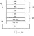
提供一种用于将电磁辐射转换为电能的光伏元件,其具有串列电池结构。该串列电池结构包括:A photovoltaic element for converting electromagnetic radiation into electrical energy is provided, which has a tandem cell structure. The tandem battery structure includes:
-染料太阳能电池,其具有第一电极、n型半导电金属氧化物、吸收第一光谱范围的电磁辐射的染料、以及固体p型半导体;以及- a dye solar cell having a first electrode, an n-type semiconducting metal oxide, a dye absorbing electromagnetic radiation in a first spectral range, and a solid p-type semiconductor; and
-有机太阳能电池,其具有受主材料和施主材料,所述受主材料和/施主材料包含有机材料,所述有机太阳能电池还包括在与所述染料太阳能电池相反的一侧上的第二电极,并且所述有机太阳能电池被配置为吸收第二光谱范围的电磁辐射,所述第二光谱范围至少部分地与所述第一光谱范围不同,- An organic solar cell having an acceptor material and a donor material, said acceptor material and/or donor material comprising an organic material, said organic solar cell further comprising a second electrode on the side opposite to said dye solar cell , and the organic solar cell is configured to absorb electromagnetic radiation in a second spectral range at least partially different from the first spectral range,
-所述第一电极和/或所述第二电极对所述电磁辐射至少部分地透明。- said first electrode and/or said second electrode are at least partially transparent to said electromagnetic radiation.
在该上下文中的术语“透明电极”旨在特别地表示在可见光谱范围内和/或太阳光谱范围(约300nm到2000nm)中的透射率为至少50%,优选至少80%。The term "transparent electrode" in this context is intended in particular to mean a transmission in the visible and/or solar spectral range (approximately 300 nm to 2000 nm) of at least 50%, preferably at least 80%.
因此,本发明涉及两种主要类型的有机太阳能电池的组合,即,具有染料敏化的金属氧化物的染料太阳能电池和包含有机单体、低聚物或聚合物(以及可选地无机纳米颗粒或其他添加剂)的有机太阳能电池的组合,至少受主材料(n型半导体)或施主材料(p型半导体)包含有机材料。除了该基础结构之外,还可以存在另外的电池,例如,其中除了所提到的染料太阳能电池和有机太阳能电池的组合之外还存在至少一个另外的电池的结构,即,例如,三电池结构。然而,在本发明的上下文中,通常具有一个层叠在另一个之上的两个电池的结构是优选的,即,其中上述部件(染料太阳能电池和有机太阳能电池)被设置或排列为一个在另一个之上作为层的结构。Thus, the present invention relates to the combination of two main types of organic solar cells, namely, dye solar cells with dye-sensitized metal oxides and organic monomers, oligomers or polymers (and optionally inorganic nanoparticles) or other additives), at least the acceptor material (n-type semiconductor) or the donor material (p-type semiconductor) contains organic materials. In addition to this basic structure there may also be further cells, for example structures in which at least one further cell is present in addition to the mentioned combination of dye solar cells and organic solar cells, i.e. for example a three-cell structure . In the context of the present invention, however, generally a structure with two cells stacked one on top of the other is preferred, i.e. where the aforementioned components (dye solar cell and organic solar cell) are arranged or arranged one on top of the other. A structure on top of one as layers.
优选地,所使用的所有材料为固体材料。此外,优选使用染料太阳能电池作为前子电池,即,面向曝光侧(exposure side)的子电池,并使用有机太阳能电池作为后子电池。还优选将有机太阳能电池中的受主材料设置在该子电池的面向染料太阳能电池的一侧上,而将施主材料设置在背离染料太阳能电池的一侧上。当从染料太阳能电池侧观察时,这优选在有机太阳能电池的内部导致np结而不是p-n结(以半导体术语表示)。然而,其他结构也是可能的。Preferably, all materials used are solid materials. Furthermore, it is preferred to use a dye solar cell as the front subcell, ie the subcell facing the exposure side, and an organic solar cell as the rear subcell. It is also preferred to arrange the acceptor material in the organic solar cell on the side of the subcell facing the dye solar cell and the donor material on the side facing away from the dye solar cell. This preferably results in an np junction rather than a p-n junction (in semiconductor terms) inside the organic solar cell when viewed from the dye solar cell side. However, other configurations are also possible.
原则上,还可将串列电池结构制造为四接触结构。然而,出于有利于制造的原因,优选地仅具有两个电极的二接触结构是优选的。在该情况下,与染料太阳能电池接触的电极(染料太阳能电池的工作电极)优选是透明的。优选地,将第一(透明)电极施加到至少部分透明的支撑物(例如刚性或透明的玻璃基板和/或塑料基板)上。在这之后是染料太阳能电池,然后是有机太阳能电池,在有机太阳能电池上又具有作为覆盖电极或顶电极的(不必是透明的)第二电极。然后,将要被转换为电能的光通过透明支撑物而首先进入染料太阳能电池,在该处光被部分地吸收(具体地,被染料吸收),之后光进入有机太阳能电池,在该处(优选在至少部分地不同的光谱范围中)光再次被至少部分地吸收(被有机材料中的至少一种,即,受主材料和/或施主材料和/或分离的吸收体,例如,掺杂的吸收体(doped-inabsorber)所吸收)。然而,还可以构思其他层结构,例如,颠倒的结构。In principle, the tandem cell structure can also be fabricated as a four-contact structure. However, a two-contact structure with preferably only two electrodes is preferred for reasons of favorable manufacturing. In this case, the electrode in contact with the dye solar cell (working electrode of the dye solar cell) is preferably transparent. Preferably, the first (transparent) electrode is applied to an at least partially transparent support, such as a rigid or transparent glass and/or plastic substrate. This is followed by a dye solar cell, and then an organic solar cell, on which again there is a second (not necessarily transparent) electrode as cover electrode or top electrode. The light to be converted to electrical energy then passes through the transparent support and first enters the dye solar cell, where it is partially absorbed (in particular, by the dye), and then enters the organic solar cell, where (preferably at At least partially in a different spectral range) the light is again at least partially absorbed (by at least one of the organic materials, i.e. acceptor material and/or donor material and/or a separate absorber, e.g. doped absorber Body (doped-inabsorber) absorbed). However, other layer structures are also conceivable, for example an inverted structure.
所提出的结构具有一系列优于已知的光伏元件的优点。具体而言,如果合适地选择施主和受主材料,可以通过有机太阳能电池更好地利用长波长光。具体而言,施主和/或受主材料可被选择为使其在近红外范围(NIR)中吸收。这可导致对太阳光谱的更好利用,因而效率更高。具体而言,可将两个子电池选择为使其互补地吸收,从而获得极高的效率。特别优选染料太阳能电池的染料具有在400nm到700nm的范围内的吸收,同时优选将有机电池的受主材料和/或施主材料选择为使其具有在600nm到1000nm的范围内的吸收。这样的选择是特别优选的,因为染料太阳能电池通常需要被制造为非常薄(典型地1-2.5微米),这导致通常不能完全利用所有的入射光。确切地说,通过如此选择有机太阳能电池的吸收,串列电池结构可以有效利用光谱的仅被小程度地利用的该长波长部分,这可以显著提高该结构的总效率。The proposed structure has a series of advantages over known photovoltaic elements. Specifically, long-wavelength light can be better utilized by organic solar cells if donor and acceptor materials are properly selected. In particular, the donor and/or acceptor material can be chosen such that it absorbs in the near infrared range (NIR). This can lead to better utilization of the solar spectrum and thus higher efficiency. In particular, the two subcells can be chosen such that they absorb complementary, resulting in extremely high efficiencies. It is particularly preferred that the dye of the dye solar cell has an absorption in the range of 400 nm to 700 nm, while the acceptor and/or donor material of the organic cell is preferably selected such that it has an absorption in the range of 600 nm to 1000 nm. Such a choice is particularly preferred since dye solar cells usually need to be fabricated very thin (typically 1-2.5 microns), which often results in incomplete utilization of all incident light. Specifically, by so selecting the absorption of the organic solar cell, the tandem cell structure can make efficient use of this long-wavelength portion of the spectrum that is only to a small extent utilized, which can significantly increase the overall efficiency of the structure.
特别地,当使用具有p型半导体的“固体电解质”取代液体或凝胶形式的电解质时,所提出的结构的另一优点在于,两个子电池的电流分量(current component)可以相对容易地彼此匹配。如上所述,公知的二接触串列电池的缺点在于,具有较小电流的子电池限制了总电流。然而,通过采用所提出的结构(例如,通过调整材料参数,选择合适的吸收体和/或调整层厚度),可以相对容易地调整两个子电池的电流。由此可以制造高效元件,其中两个子电池的光电压被相加而给出高的总电压。此外,所提出的电池结构还避免了从现有技术已知的利用染料双重敏化并使用液体电解质的He,Hagfeldt等人和von Nakasa等人的串列电池构思的上述缺点,并且其允许例如可通过单个连续生产线的制造技术制造的显著简化的电池结构。具体而言,可以避免需要双重染料敏化(敏化的氧化物阳极和敏化的氧化物阴极)的由Hagfeldt等人描述的结构。In particular, another advantage of the proposed structure is that the current components of the two subcells can be matched to each other relatively easily when a "solid electrolyte" with p-type semiconductor is used instead of the electrolyte in liquid or gel form. . As mentioned above, a disadvantage of the known two-contact tandem cells is that the sub-cells with the lower current limit the total current. However, by adopting the proposed structure (e.g., by tuning material parameters, choosing a suitable absorber, and/or tuning layer thickness), the currents of the two subcells can be tuned relatively easily. This makes it possible to produce highly efficient components in which the photovoltages of the two subcells are added to give a high overall voltage. Furthermore, the proposed cell structure avoids the above-mentioned disadvantages from the tandem cell concepts of He, Hagfeldt et al. and von Nakasa et al. A significantly simplified battery structure that can be fabricated by a single continuous line manufacturing technique. In particular, the structure described by Hagfeldt et al. which requires double dye sensitization (sensitized oxide anode and sensitized oxide cathode) can be avoided.
可以以各种方式有利地配置或发展上面提出的基础结构。在从属权利要求中给出了这些发展中的一些,并且下面将描述一些优选的选项。对于其他可能的细节,可以参考以下实例以及在介绍部分中描述的在现有技术中给出的材料和技术。The infrastructure presented above can be advantageously configured or developed in various ways. Some of these developments are given in the dependent claims and some preferred options are described below. For further possible details, reference is made to the following examples and to the materials and techniques given in the prior art described in the introductory section.
1.染料太阳能电池1. Dye solar cells
第一电极和n型半导电金属氧化物First electrode and n-type semiconducting metal oxide
可以使用单金属氧化物或不同氧化物的混合物作为染料太阳能电池的n型半导电金属氧化物。还可以使用混合的氧化物。特别地,使用n型半导电金属氧化物作为纳米颗粒氧化物,在该上下文中,纳米颗粒旨在表示具有小于0.1微米的平均颗粒尺寸的颗粒。Single metal oxides or mixtures of different oxides can be used as n-type semiconducting metal oxides for dye solar cells. Mixed oxides may also be used. In particular n-type semiconducting metal oxides are used as nanoparticle oxides, in this context nanoparticles are intended to mean particles having an average particle size of less than 0.1 micrometer.
常规地通过烧结工艺在导电基板(即,具有作为第一电极的导电层的支撑物)上将纳米颗粒氧化物施加为具有大表面积的薄多孔膜。Nanoparticle oxides are conventionally applied by a sintering process as a thin porous film with a large surface area on a conductive substrate (ie a support with a conductive layer as a first electrode).
除了金属箔之外,上述所有的塑料板或片以及特别地玻璃板同样适于作为基板(以下也称为支撑物)。特别地,导电材料,例如透明导电氧化物(TCO)(例如掺杂有氟和/或铟的氧化锡(分别为FTO和ITO)和/或铝掺杂的氧化锌(AZO))、碳纳米管或金属膜适于作为电极材料,特别是对于根据上述优选结构的第一电极而言。然而,替代地或附加地,还可以使用仍具有足够的透明度的薄金属膜。用这些导电材料覆盖或涂覆基板。In addition to metal foils, all plastic plates or sheets mentioned above and in particular glass plates are also suitable as substrates (hereinafter also referred to as supports). In particular, conductive materials such as transparent conductive oxides (TCO) such as tin oxide doped with fluorine and/or indium (FTO and ITO, respectively) and/or aluminum-doped zinc oxide (AZO)), carbon nano A tube or a metal film is suitable as electrode material, in particular for the first electrode according to the preferred structure described above. Alternatively or additionally, however, it is also possible to use thin metal films which still have sufficient transparency. Cover or coat the substrate with these conductive materials.
因为所提出的结构通常仅仅需要单个基板,因此还可以构建挠性(flexible)电池。这允许用刚性基板所不能实施或难以实施的多种应用任务,例如,用于银行卡、衣物等。Since the proposed structure generally requires only a single substrate, flexible batteries can also be constructed. This allows a wide variety of application tasks that are impossible or difficult to implement with rigid substrates, eg for bank cards, clothing, etc.
第一电极,特别地TCO层,可以附加地覆盖或涂覆有(例如,10-200nm厚)固体缓冲层(特别地,金属氧化物缓冲层),以避免p型半导体直接接触TCO层(参见Peng et al.,Coord.Chem.Rev.248,1479(2004))。例如,可以用于缓冲层的缓冲金属氧化物包含以下材料中的一种或多种:氧化钒;氧化锌;氧化锡;氧化钛。然而,与液体或凝胶形式的电解质相比,本发明对固体p型半导电电解质的使用极大地减小了电解质与第一电极的接触,这使得在一些情况下该缓冲层是不必要的,从而在一些情况下可以略去该层,因为该层具有电流限制作用并且还会劣化n型半导电金属氧化物与第一电极的接触。这提高了部件的效率。另一方面,这样的缓冲层转而可以被用于方便地匹配染料太阳能电池的电流分量与有机太阳能电池的电流分量。对于其中已经略去缓冲层的电池,特别是固体电池,经常还会发生电荷载流子的不希望的复合的问题。在这方面,特别地在固体电池中,在一些情况下缓冲层是有利的。The first electrode, in particular the TCO layer, may additionally be covered or coated with (e.g., 10-200 nm thick) a solid buffer layer (in particular, a metal oxide buffer layer) to avoid direct contact of the p-type semiconductor with the TCO layer (see Peng et al., Coord. Chem. Rev. 248, 1479 (2004)). For example, buffer metal oxides that may be used in the buffer layer include one or more of the following materials: vanadium oxide; zinc oxide; tin oxide; titanium oxide. However, the present invention's use of a solid p-type semiconducting electrolyte greatly reduces the contact of the electrolyte with the first electrode compared to electrolytes in liquid or gel form, which makes this buffer layer unnecessary in some cases , so that this layer can be omitted in some cases because it has a current confinement effect and also degrades the contact of the n-type semiconducting metal oxide with the first electrode. This increases the efficiency of the component. On the other hand, such a buffer layer can in turn be used to conveniently match the current component of the dye solar cell to that of the organic solar cell. For batteries, in particular solid-state batteries, in which the buffer layer has been omitted, the problem of undesired recombination of charge carriers often also occurs. In this respect, especially in solid-state batteries, buffer layers are advantageous in some cases.
公知金属氧化物的薄层或膜通常代表经济的固体半导体材料(n型半导体),虽然由于大的带隙,其吸收通常并不位于电磁谱的可见光范围内而是多数位于紫外光谱范围内。对于在太阳能电池中的应用,与染料太阳能电池的情况相同地,金属氧化物通常必须与作为感光剂(photosensitizer)的染料组合,该染料在太阳光的波长范围(即,300-2000nm)内进行吸收并在电子受激态下向半导体的导带注射电子。在电池中附加地用作电解质的固体p型半导体的帮助下,该电解质转而在背电极(或在与串列太阳能电池的第二子电池的结)处被还原,电子可以返回到敏化剂(sensitizer)以便被再生。It is known that thin layers or films of metal oxides generally represent economical solid semiconductor materials (n-type semiconductors), although their absorption is generally not in the visible range of the electromagnetic spectrum but mostly in the ultraviolet spectral range due to the large band gap. For application in solar cells, as in the case of dye solar cells, metal oxides generally have to be combined with dyes as photosensitizers that operate within the wavelength range of sunlight (ie, 300-2000nm). Absorbs and injects electrons into the conduction band of the semiconductor in an electronically excited state. With the help of a solid p-type semiconductor additionally used as an electrolyte in the cell, which in turn is reduced at the back electrode (or at the junction with the second subcell of the tandem solar cell), electrons can return to the sensitized agent (sensitizer) in order to be regenerated.
对于在太阳能电池中的应用,半导体氧化锌、氧化锡、二氧化钛、或这些金属氧化物的混合物尤其受到关注。采用纳米晶体多孔层形式的金属氧化物。这些层具有被敏化剂涂覆的大表面积,以便实现对太阳光的高吸收。例如纳米棒构建的金属氧化物层提供了诸如较高的电子迁移率或染料的改善的孔填充能力的优点。For use in solar cells, the semiconductors zinc oxide, tin oxide, titanium dioxide, or mixtures of these metal oxides are of particular interest. Metal oxides in the form of nanocrystalline porous layers. These layers have a large surface area coated with sensitizers in order to achieve high absorption of sunlight. For example nanorod-structured metal oxide layers offer advantages such as higher electron mobility or improved hole-filling ability of dyes.
可以单独地或以混合物的形式使用金属氧化物半导体。还可以用一种或多种金属氧化物来涂覆金属氧化物。此外,还可以将金属氧化物施加为在另一半导体(例如,GaP、ZnP或ZnS)上的涂层。Metal oxide semiconductors may be used alone or in the form of a mixture. Metal oxides may also be coated with one or more metal oxides. Furthermore, the metal oxide can also be applied as a coating on another semiconductor (eg GaP, ZnP or ZnS).
优选以纳米晶体形式使用的锐钛矿变体(modification)的氧化锌和二氧化钛是特别优选的半导体。Zinc oxide and titanium dioxide of the anatase modification, preferably used in nanocrystalline form, are particularly preferred semiconductors.
此外,可以有利地使敏化剂与通常用于这些太阳能电池的所有n型半导体组合。可以提及用于陶瓷的金属氧化物作为优选的实例,例如,二氧化钛、氧化锌、氧化锡(IV)、氧化钨(VI)、氧化钽(V)、氧化铌(V)、氧化铯、钛酸锶、锡酸锌、钙钛矿类型的复合氧化物,例如钛酸钡、以及二元和三元铁氧化物,其同样以纳米晶体或非晶形式存在。Furthermore, sensitizers can advantageously be combined with all n-type semiconductors commonly used for these solar cells. Metal oxides for ceramics may be mentioned as preferred examples, for example titanium dioxide, zinc oxide, tin(IV) oxide, tungsten(VI) oxide, tantalum(V) oxide, niobium(V) oxide, cesium oxide, titanium Strontium oxide, zinc stannate, complex oxides of the perovskite type, such as barium titanate, and binary and ternary iron oxides, which also exist in nanocrystalline or amorphous form.
由于常规有机染料以及酞菁和卟啉类化合物显示出的强吸收,即使n型半导电金属氧化物的薄层或膜也足以接收所需量的染料。薄金属氧化物膜转而具有这样的优点,即,降低了不希望的复合过程的可能性并且减小了染料太阳能电池的内阻。对于n型半导电金属氧化物,优选使用的层厚度为100nm到20微米,特别优选在500nm到约3微米的范围内。Due to the strong absorption exhibited by conventional organic dyes as well as phthalocyanines and porphyrins, even thin layers or films of n-type semiconducting metal oxides are sufficient to receive the required amount of dye. Thin metal oxide films in turn have the advantage of reducing the possibility of undesired recombination processes and reducing the internal resistance of the dye solar cell. For n-type semiconducting metal oxides, preferably used layer thicknesses are in the range from 100 nm to 20 micrometers, particularly preferably in the range from 500 nm to about 3 micrometers.
染料dye
从现有技术可知在本发明的范围内使用的许多染料,因此,对于可能的材料实例,也可以参考以上关于染料太阳能电池的现有技术的描述。原则上,所提到的和要求保护的所有染料还呈现作为颜料(pigment)。例如,在US-A-4927721、Nature353,pp.737-740(1991)和US-A-5350644以及Nature395,pp.583-585(1998)和EP-A-1176646中描述了基于作为半导体材料的二氧化钛的染料敏化的太阳能电池。在本发明的范围中,原则上同样可以有利地应用这些文献中描述的染料。这些染料太阳能电池包含过渡金属络合物(特别地,钌络合物)的单分子膜,其通过酸基团(acidgroup)而被接合到二氧化钛层作为敏化剂。Many dyes to be used within the scope of the present invention are known from the prior art, so reference is also made to the above description of the prior art on dye solar cells for examples of possible materials. In principle, all dyes mentioned and claimed are also present as pigments. For example, in US-A-4927721, Nature 353, pp.737-740 (1991) and US-A-5350644 and Nature 395, pp.583-585 (1998) and EP-A-1176646 described based on as semiconductor material Titanium dioxide dye-sensitized solar cells. Within the scope of the present invention, the dyes described in these documents can also be advantageously used in principle. These dye solar cells comprise monomolecular films of transition metal complexes, in particular ruthenium complexes, which are bonded to the titanium dioxide layer via acid groups as sensitizers.
特别是由于成本原因,不含金属的有机染料也被再三提出作为敏化剂,在本发明的范围中同样也可采用不含金属的有机染料。例如,利用二氢吲哚染料,尤其在固体染料太阳能电池中,可以实现大于4%的效率(参见例如,Schmidt-Mende et al.,Adv.Mater.2005,17,813)。US-A-6359211描述了花青、
JP-A-10-189065、2000-243463、2001-093589、2000-100484以及10-334954描述了用于半导体太阳能电池的各种苝-3,4:9,10-四羧酸衍生物,这些衍生物在苝主链中未被取代。具体而言,这些衍生物为:苝四羧酸二酰亚胺,其在酰亚胺氮原子上携带羧烷基、羧基芳基、羧基芳基烷基或羧基烷基芳基和/或被对二氨基苯酰亚胺化,其中对位的氨基的氮原子被两个另外的苯基取代或者是杂芳三环体系的一部分;苝-3,4:9,10-四羧酸单酐单酰亚胺,其在酰亚胺氮原子上携带上述基团或未进一步官能化的烷基或芳基基团,或苝-3,4,9,10-四羧酸二酐与1,2-二氨基苯或1,8-二氨基萘的半缩合物,其通过与伯胺进一步反应而转变为对应的二酰亚胺或双缩合物;苝-3,4,9,10-四羧酸二酐与通过羧基或氨基基团官能化的1,2-二氨基苯的缩合物;以及用脂肪或芳香二胺酰亚胺化的苝-3,4:9,10-四羧酸二酰亚胺。JP-A-10-189065, 2000-243463, 2001-093589, 2000-100484 and 10-334954 describe various perylene-3,4:9,10-tetracarboxylic acid derivatives for semiconductor solar cells, these The derivatives are unsubstituted in the perylene backbone. Specifically, these derivatives are: perylenetetracarboxylic acid diimides, which carry carboxyalkyl, carboxyaryl, carboxyarylalkyl or carboxyalkylaryl groups on the imide nitrogen atom and/or are imidization of p-diaminobenzene, in which the nitrogen atom of the amino group in the para position is substituted by two additional phenyl groups or is part of a heteroaromatic tricyclic ring system; perylene-3,4:9,10-tetracarboxylic monoanhydride Monoimides bearing the abovementioned groups or not further functionalized alkyl or aryl groups on the imide nitrogen atom, or perylene-3,4,9,10-tetracarboxylic dianhydrides with 1, Hemicondensates of 2-diaminobenzene or 1,8-diaminonaphthalene, which are converted to the corresponding imides or biscondensates by further reaction with primary amines; perylene-3,4,9,10-tetra Condensates of carboxylic dianhydrides with 1,2-diaminobenzene functionalized via carboxyl or amino groups; and perylene-3,4:9,10-tetracarboxylic acids imidized with aliphatic or aromatic diamines Diimide.
New J.Chem.26,pp.1155-1160(2002)研究了具有苝衍生物(在苝主链上未取代(湾位置))的二氧化钛的敏化性。具体地提到9-二烷基氨基苝-3,4-二羧酸酐,苝-3,4-二羧酸酰亚胺,其在9-位由二烷基氨基或羧甲基氨基取代并且在酰亚胺氮原子上携带羧甲基或2,5-二(叔丁基)苯基基团、以及正十二烷基氨基苝-3,4:9,10-四羧酸单酐单酰亚胺。然而,基于这些苝衍生物的液体电解质电池呈现比用钌络合物敏化的太阳能电池显著低的效率。New J. Chem. 26, pp. 1155-1160 (2002) studied the sensitization of titanium dioxide with perylene derivatives (unsubstituted (Bay position) on the perylene backbone). Specifically mentioned are 9-dialkylaminoperylene-3,4-dicarboxylic anhydrides, perylene-3,4-dicarboxylic imides, which are substituted at the 9-position by dialkylamino or carboxymethylamino and Carboxymethyl or 2,5-bis(tert-butyl)phenyl group, and n-dodecylaminoperylene-3,4:9,10-tetracarboxylic monoanhydride monoanhydride on the imide nitrogen atom imide. However, liquid electrolyte cells based on these perylene derivatives exhibit significantly lower efficiencies than solar cells sensitized with ruthenium complexes.
在所提出的染料太阳能电池中的特别优选作为敏化剂染料的为在DE102005053995A1或WO2007/054470A1中描述的苝衍生物、三并苯(terylene)衍生物以及四并苯(quaterrylene)衍生物。这些染料的使用使光伏元件具有高效率并同时具有高稳定性。Particularly preferred as sensitizer dyes in the proposed dye solar cells are the perylene, terylene and quaterrylene derivatives described in
并苯类(rylenes)呈现出在太阳光的波长范围内的吸收,并在该情况下依赖于共轭系统的长度而覆盖从约400nm(DE102005053995A1中的苝衍生物I)到约900nm(DE102005053995A1中的四并苯衍生物)的范围。依赖于其组成,基于被吸附在二氧化钛上的固态三并苯的并苯(rylene)衍生物I在从约400到800nm的范围内吸收。为了实现最大范围地利用从可见光到红外范围的入射太阳光,使用不同的并苯衍生物I的混合物是有利的。有时还建议在该情况下使用不同的并苯同族体。Rylenes exhibit absorption in the wavelength range of sunlight and in this case cover from about 400 nm (perylene derivatives I in
并苯衍生物I可以被容易地且永久地固定在金属氧化物膜上。在该情况下,通过酐官能团(x1)或原位形成的羧基-COOH或-COO-或通过包含在酰亚胺或缩合物基团((x2)或(x3))中的酸基团A进行结合。在DE102005053995A1中描述的并苯衍生物I非常适合用于本发明的范围内的染料敏化的太阳能电池。Acene derivatives I can be easily and permanently immobilized on metal oxide films. In this case, via the anhydride function (x1) or the carboxyl group -COOH or -COO- formed in situ or via the acid group A contained in the imide or condensate group ((x2) or (x3)) to combine. The acene derivatives I described in
特别优选地,染料包含位于分子的一端处的锚定基团,该基团将染料固定到n型半导体膜。在分子的另一端处,染料优选包含电子施主Y,其有助于在电子传递到n型半导体之后的使染料再生,此外还防止已被传递到半导体的电子的复合。Particularly preferably, the dye contains an anchor group at one end of the molecule, which fixes the dye to the n-type semiconductor film. At the other end of the molecule, the dye preferably contains an electron donor Y, which helps regenerate the dye after electron transfer to the n-type semiconductor, and also prevents recombination of electrons that have been transferred to the semiconductor.
关于合适的染料的可能的选择的进一步的细节,可以再次参考例如DE102005053995A1。具体而言,钌络合物、卟啉、其他有机敏化剂以及优选的并苯可以用于这里描述的串列电池。For further details on the possible selection of suitable dyes, reference can again be made to eg
以直接的方式来将染料固定在金属氧化物膜上。例如,使新烧结(仍温)状态的n型半导电金属氧化物膜与染料在合适的有机溶剂中的溶液或悬浊液接触足够的时长(例如,0.5到24小时)。例如,这可以通过将涂覆有金属氧化物的基板浸入到染料溶液中而实现。Immobilization of dyes on metal oxide films in a direct manner. For example, a freshly sintered (still warm) n-type semiconducting metal oxide film is contacted with a solution or suspension of a dye in a suitable organic solvent for a sufficient period of time (eg, 0.5 to 24 hours). For example, this can be achieved by dipping the metal oxide coated substrate into a dye solution.
如果希望使用不同染料的组合,那么可以从包含一种或多种染料的一种或多种溶液或悬浊液来连续施加染料。还可以使用通过例如CuSCN的层而分离的两种染料(关于这一点,例如,参见Tennakone,K.J.,Phys.Chem.B.2003,107,13758)。可以在个体情况下相对容易地确定最有利的方法。If it is desired to use a combination of different dyes, the dyes can be applied sequentially from one or more solutions or suspensions containing one or more dyes. It is also possible to use two dyes separated by a layer such as CuSCN (see, for example, Tennakone, K.J., Phys. Chem. B. 2003, 107, 13758 in this regard). The most favorable method can be determined relatively easily in individual circumstances.
关于染料和氧化物颗粒尺寸的选择,将太阳能电池配置为使两个子电池吸收尽可能多的光。出于该原因,如上所述,应尽可能互补地选择染料。在该情况下,氧化物层应被构造为使固体p型半导体可以很好地填充孔。With regard to the choice of dye and oxide particle size, the solar cell is configured such that both subcells absorb as much light as possible. For this reason, as mentioned above, the dyes should be chosen as complementary as possible. In this case, the oxide layer should be structured such that the solid p-type semiconductor can fill the pores well.
原则上,染料可以作为单独的要素而存在,或者在单独的步骤中施加和被单独施加到剩余的层。然而,替代地或附加地,也可以与一种或多种其他要素(例如与固体p型半导体)组合或一起施加染料。例如,可以使用染料-p型半导体组合,其包含具有p型半导电特性的吸收剂染料或例如具有吸收和p型半导电特性的颜料。In principle, the dye can be present as a separate element, or be applied in a separate step and be applied separately to the remaining layers. Alternatively or additionally, however, the dye may also be applied in combination or together with one or more other elements, for example with a solid p-type semiconductor. For example, a dye-p-type semiconductor combination comprising an absorber dye with p-type semiconducting properties or eg a pigment with absorbing and p-type semiconducting properties may be used.
如上所述,所提出的串列电池构思包括使用一种或多种固体p型半导体。虽然优选独占地使用至少一种p型半导体,但除了固体p型半导体(例如,固体电解质)之外自然还存在具有类似特性的其他材料。为了防止n型半导电金属氧化物中的电子与固体p型半导体复合,使用包含钝化材料的一种钝化层。该层应尽可能地薄,并应尽可能地仅仅覆盖n型半导电金属氧化物的先前未覆盖的位置。在特定的环境下,钝化层还可以在时间上先于染料而被施加到金属氧化物上。特别地,优选以下物质作为钝化材料:Al2O3;铝盐;硅烷,例如,CH3SiCl3;有机金属络合物,特别地,Al3+络合物;Al3+,特别地,Al3+络合物;4-叔丁基吡啶(TBP);MgO;4-胍基丁基酸(GBA);烷基酸;十六烷基丙二酸(HDMA)。As mentioned above, the proposed tandem cell concept involves the use of one or more solid p-type semiconductors. Although it is preferred to use exclusively at least one p-type semiconductor, there are naturally other materials with similar properties besides solid p-type semiconductors (eg, solid electrolytes). To prevent electrons in the n-type semiconducting metal oxide from recombining with the solid p-type semiconductor, a passivation layer comprising passivation material is used. This layer should be as thin as possible and should cover as far as possible only the previously uncovered locations of the n-type semiconducting metal oxide. Under certain circumstances, the passivation layer can also be applied to the metal oxide temporally prior to the dye. In particular, the following are preferred as passivation materials: Al2 O3 ; aluminum salts; silanes, eg CH3 SiCl3 ; organometallic complexes, especially Al3+ complexes; Al3+ , especially , Al3+ complex; 4-tert-butylpyridine (TBP); MgO; 4-guanidinobutyric acid (GBA); alkanoic acid; hexadecylmalonic acid (HDMA).
p型半导体p-type semiconductor
如上所述,在这里所提出的串列构思的范围中使用固体p型半导体。特别地当染料强吸收且因此仅仅需要薄n型半导体层时,在根据本发明的染料敏化的子电池中可以采用固体p型半导体,而不极大地增大电池电阻。特别地,p型半导体应实质上包括连续的致密层,以避免由n型半导电金属氧化物(特别地,纳米多孔形式)与第二电极或第二子电池之间的接触导致的不希望的复合反应。As mentioned above, solid p-type semiconductors are used within the scope of the tandem concept presented here. Especially when the dye absorbs strongly and thus only a thin n-type semiconductor layer is required, a solid p-type semiconductor can be employed in the dye-sensitized subcells according to the invention without greatly increasing the cell resistance. In particular, the p-type semiconductor should substantially comprise a continuous dense layer to avoid undesired contact between the n-type semiconducting metal oxide (in particular, nanoporous form) and the second electrode or second subcell compound reaction.
影响p型半导体的选择的基本量是空穴迁移率,因为这连带确定了空穴扩散长度(参见Kumara,G.,Langmuir,2002,18,10493-10495)。例如在Saragi,T.,Adv.Funct.Mater.2006,16,966-974中可以找到各种螺化合物的电荷载流子迁移率的比较。A fundamental quantity affecting the choice of p-type semiconductor is the hole mobility, since this in turn determines the hole diffusion length (cf. Kumara, G., Langmuir, 2002, 18, 10493-10495). A comparison of the charge carrier mobilities of various spiro compounds can be found eg in Saragi, T., Adv. Funct. Mater. 2006, 16, 966-974.
固体p型半导体的实例为无机固体,例如,碘化铜(I)和硫氰酸铜(I)。然而,优选使用有机半导体(即,低分子量、低聚或聚合半导体、或者这样的半导体的混合物)。在该情况下的实例为基于诸如聚噻吩和聚芳基胺的聚合物或者基于诸如在介绍部分中提到的螺二芴的非晶的可逆地可氧化的非聚合有机化合物的p型半导体(参见,例如,US2006/0049397,螺化合物在其中被公开作为p型半导体,并同样可以在本发明的范围内使用)。可以以未掺杂或掺杂的形式使用这些固体p型半导体。Examples of solid p-type semiconductors are inorganic solids such as copper(I) iodide and copper(I) thiocyanate. However, preference is given to using organic semiconductors (ie low molecular weight, oligomeric or polymeric semiconductors, or mixtures of such semiconductors). Examples in this case are p-type semiconductors based on polymers such as polythiophenes and polyarylamines or on amorphous, reversibly oxidizable non-polymeric organic compounds such as spirobifluorenes mentioned in the introduction ( See, for example, US 2006/0049397, in which spiro compounds are disclosed as p-type semiconductors and can likewise be used within the scope of the present invention). These solid p-type semiconductors can be used in undoped or doped form.
此外,还可以参考对现有技术的描述中的关于p型半导电材料的评论。对于其他可能的要素和染料太阳能电池的可能的结构同样可以基本上参考以上描述。In addition, reference may also be made to the comments on p-type semiconducting materials in the description of the prior art. For the other possible elements and possible structures of the dye solar cell, reference is likewise substantially made to the above description.
2.染料太阳能电池与有机太阳能电池之间的可选的电荷复合区域2. Optional charge recombination area between dye solar cells and organic solar cells
因为这里提出的光伏元件是根据串列构思的元件,应该确保来自有机太阳能电池的n型半导体的电子以最小的能量损失与来自染料太阳能电池的p型半导体的空穴复合。否则,电荷载流子不能彼此复合(这会导致极大地抑制光电流),或者电压损耗变为非常大。Since the photovoltaic element proposed here is an element according to the tandem concept, it should be ensured that the electrons from the n-type semiconductor of the organic solar cell recombine with the holes from the p-type semiconductor of the dye solar cell with minimal energy loss. Otherwise, the charge carriers cannot recombine with each other (which leads to greatly suppressed photocurrent), or the voltage loss becomes very large.
在本发明的优选配置中,由此在两个子电池之间使用电荷复合区域,以便俘获染料太阳能电池的空穴和有机太阳能电池的电子。在WO02/101838中描述了类似的构思。电荷复合区域应至少在入射方向下游的第二子电池所主要吸收的光谱范围中是至少部分透明的,以便同样充分曝光第二子电池(例如,有机太阳能电池)。因此,该电荷复合区域应优选尽可能地薄,优选薄于

作为对复合材料(例如,上述材料)故意引入的替代或附加,还可以使用其他构思以产生电荷复合区域。例如,可以使用会导致电荷复合区域中的电子-空穴复合的电活性缺陷。对于这一点,例如,在电荷复合区域中,故意地限制性地将缺陷引入到层结构中或在染料太阳能电池与有机太阳能电池之间的界面中。用作电活性缺陷的这些缺陷可通过控制性地引入杂质、在沉积各有机层期间暴露到高能粒子辐射而产生,或通过其他技术产生。还可以使用微波辐射、等离子体处理或利用由微波激发的粒子的处理。这样的用于通过相应处理故意引入缺陷的方法是公知的并可以被采用,例如,通过无机半导体制造技术。替代地或附加地,电荷复合中心还可以包括高掺杂的p/n结,即,包括这样的区域,其中所使用的材料比其余层的掺杂更高。As an alternative or in addition to deliberate introduction of composite materials such as those described above, other concepts can also be used to create charge recombination regions. For example, electrically active defects that lead to electron-hole recombination in the charge recombination region can be used. For this, for example, in the charge recombination region, defects are introduced in a deliberate and limited manner into the layer structure or in the interface between the dye solar cell and the organic solar cell. These defects, which serve as electrically active defects, can be created by the controlled introduction of impurities, exposure to energetic particle radiation during deposition of the respective organic layers, or by other techniques. Microwave radiation, plasma treatment or treatment with particles excited by microwaves may also be used. Such methods for intentionally introducing defects by corresponding treatments are known and can be employed, for example, by inorganic semiconductor manufacturing technology. Alternatively or additionally, the charge recombination centers can also comprise highly doped p/n junctions, ie regions in which the material used is more highly doped than the remaining layers.
3.有机太阳能电池3. Organic solar cells
如上所述,有机太阳能电池优选直接在染料太阳能电池之后或经由电荷复合区域而在染料太阳能电池之后。优选地,与上述相似,在支撑物上首先沉积染料太阳能电池,然后施加有机太阳能电池。在该情况下,在已经存在的染料太阳能电池上沉积(直接沉积或在施加/引入电荷复合区域之后沉积)有机太阳能电池。As mentioned above, the organic solar cell preferably follows the dye solar cell either directly or via a charge recombination region. Preferably, similarly to the above, the dye solar cells are first deposited on the support and the organic solar cells are then applied. In this case, the organic solar cells are deposited (directly or after application/introduction of charge recombination regions) on already existing dye solar cells.
利用有机太阳能电池,本发明的串列电池结构显示出特别的优势,这是因为,由于在层内部的电荷和/或激子输运的要求,有机太阳能电池通常被制造为非常薄。然而,随着厚度减小,光吸收效率也降低。该有害的影响可以通过串列电池构思而减轻。With organic solar cells, the tandem cell structure of the invention shows particular advantages, since organic solar cells are usually produced very thin due to the requirements for charge and/or exciton transport within the layers. However, as the thickness decreases, the light absorption efficiency also decreases. This detrimental effect can be mitigated by the tandem cell concept.
有机太阳能电池包括至少一种受主材料(n型半导体)和至少一种施主材料(p型半导体),它们在p-n结处彼此直接或间接接触,但还可以存在中间层(类似于p-i-n结)。替代上面和下面描述的层和多层结构,替代地或附加地,通常还可以全部或部分地使用所述材料的混合层,即,例如,单个混合材料层取代具有两种独立的(separate)材料的两层结构(例如,受主材料层和施主材料层)。还可以在两个独立的层之间存在过渡层,例如,受主材料层、具有受主材料和施主材料的混合物的中间层(这在理论上涉及“体异质结”,参见下面的描述)、以及随后的施主材料层。此外,可以使用所谓的“体异质结”,即,太阳能电池技术领域中公知的结构,其中在两层(例如受主材料层与施主材料层)之间存在具有极大地扩展的表面积的边界层。在该情况下,各层彼此啮合,并沿非常不平坦的界面具有多个“脊”和“槽”。特别地,该体异质结可以被有利地用于有机太阳能电池的受主-施主材料结构。Organic solar cells comprise at least one acceptor material (n-type semiconductor) and at least one donor material (p-type semiconductor), which are in direct or indirect contact with each other at a p-n junction, but intermediate layers may also be present (similar to a p-i-n junction) . Instead of the layers and multilayer structures described above and below, alternatively or additionally it is also generally possible to use mixed layers of said materials in whole or in part, i.e. for example a single mixed material layer instead of having two separate (separate) A two-layer structure of materials (eg, a layer of acceptor material and a layer of donor material). There can also be a transition layer between two separate layers, e.g. a layer of acceptor material, an intermediate layer with a mixture of acceptor material and donor material (this theoretically involves a "bulk heterojunction", see description below ), and a subsequent layer of donor material. Furthermore, so-called "bulk heterojunctions" can be used, i.e. structures well known in the field of solar cell technology in which there is a boundary with a greatly expanded surface area between two layers (e.g. a layer of acceptor material and a layer of donor material). layer. In this case, the layers engage each other with multiple "ridges" and "troughs" along very uneven interfaces. In particular, the bulk heterojunction can be advantageously used in the acceptor-donor material structure of organic solar cells.
因此,有机太阳能电池优选包括位于受主材料层与施主材料层之间的过渡区,受主材料层被设置在面向染料太阳能电池的一侧,施主材料层被设置在过渡区的背离染料太阳能电池的一侧(n/p结)。该过渡区被配置为在n型层与p型层之间的直接过渡,但其可以附加地在受主材料层与施主材料层之间包括至少一种受主材料与至少一种施主材料的混合层(即,体异质结)。例如,该过渡区和该过渡区的层优选全部或部分地以聚合物层(例如,从溶液或分散体(dispersion)产生)的形式和/或颜料(优选地,气相沉积和/或从分散体产生)或染料(优选从溶液或分散体产生),即,低分子量有机材料的形式产生。Accordingly, the organic solar cell preferably comprises a transition region between a layer of acceptor material arranged on the side facing the dye solar cell and a layer of donor material arranged on the side of the transition region facing away from the dye solar cell. side (n/p junction). The transition region is configured as a direct transition between the n-type layer and the p-type layer, but it may additionally comprise at least one acceptor material and at least one donor material between the acceptor material layer and the donor material layer Mixed layers (ie, bulk heterojunction). For example, the transition zone and the layers of the transition zone are preferably wholly or partly in the form of polymer layers (eg produced from solution or dispersion) and/or pigments (preferably vapor-deposited and/or from dispersion produced as solids) or dyes (preferably produced from solutions or dispersions), ie in the form of low molecular weight organic materials.
这两种材料(受主材料和/或施主材料)中的至少一种应至少部分地吸收电极辐射,即,特别地,光。该吸收应被特别地选择为使其与染料太阳能电池的吸收“互补”,即,至少是不全等的。例如,优选染料太阳能电池的主吸收(例如,吸收最大值)的波长范围比有机太阳能电池短(即,能量更大)。例如,如上所述,优选有机太阳能电池在600nm到1000nm之间的范围内吸收(虽然该波长范围自然地不需被完全覆盖,且自然地还可以存在其他范围内的吸收),而染料太阳能电池优选在400nm到700nm之间的范围内吸收(同样,自然地可以不完全覆盖该范围和/或同样存在在其他范围内的吸收)。然而,原则上,相反的配置同样是可能的,即,其中染料太阳能电池的主吸收的波长范围比有机太阳能电池更长。At least one of the two materials (acceptor material and/or donor material) should at least partially absorb electrode radiation, ie, in particular light. This absorption should be specifically chosen so that it is "complementary", ie at least not congruent, to that of the dye solar cell. For example, dye solar cells preferably have a wavelength range of main absorption (eg, absorption maximum) that is shorter (ie, more energetic) than organic solar cells. For example, as mentioned above, it is preferred that organic solar cells absorb in the range between 600nm and 1000nm (although naturally this wavelength range need not be completely covered, and naturally there may also be absorption in other ranges), while dye solar cells Preference is given to absorption in the range between 400 nm and 700 nm (again, naturally this range may not be completely covered and/or absorption in other ranges may also be present). In principle, however, the opposite configuration is also possible, ie in which the wavelength range of the main absorption of the dye solar cell is longer than that of the organic solar cell.
当施加有机太阳能电池时,优选首先施加受主材料(n型材料),即,例如,在上述结构中该材料最靠近染料太阳能电池。为了以电子有效的方式(electronically efficient manner)将有机太阳能电池耦合到电荷复合区域,至少在后者与有机太阳能电池的受主材料之间引入至少一个电子输运层(ETL)。电子输运层通常被理解为表示具有电子传导或电子输运特性的一种或多种材料的层。根据需要,该ETL还可以为n掺杂的。然后将有机太阳能电池的施主材料(p型材料)施加到受主材料,经常在结处形成或故意引入n型与p型材料的混合层。When applying the organic solar cell, it is preferred to apply the acceptor material (n-type material) first, ie, for example, the material closest to the dye solar cell in the structure described above. In order to couple an organic solar cell to the charge recombination region in an electronically efficient manner, at least one electron transport layer (ETL) is introduced at least between the latter and the acceptor material of the organic solar cell. An electron-transport layer is generally understood to mean a layer of one or more materials having electron-conducting or electron-transporting properties. The ETL can also be n-doped if desired. The donor material (p-type material) of the organic solar cell is then applied to the acceptor material, often forming or intentionally introducing a mixed layer of n-type and p-type material at the junction.
特别地,电子输运层(还可以以相应的方式提供多个电子输运层)包含以下材料中的一种或多种:苯并菲衍生物;1,3-二(4-叔丁基苯基-1,3,4-二唑基)亚苯基(OXD7);1,3-二(4-(N,N-二甲基氨基)苯基-1,3,4-

特别地,当使用可溶材料时,作为顺序沉积受主和施主材料的备选方案,可以同时完全或部分地沉积这些材料,然后例如对其退火。例如,颜料可以通过气相沉积和/或从分散体施加,并且染料或聚合物从溶液施加。例如,可以使用两种气相沉积的材料或两种可溶材料,但还可以设想使用可溶和气相沉积的材料的组合。In particular, when using soluble materials, as an alternative to depositing the acceptor and donor materials sequentially, these materials may be deposited in whole or in part simultaneously and then eg annealed. For example, pigments may be applied by vapor deposition and/or from dispersion, and dyes or polymers from solution. For example, two vapor-deposited materials or two soluble materials may be used, although a combination of soluble and vapor-deposited materials is also conceivable.
原则上,在现有技术中描述的以及在介绍部分中部分给出的有机半导体可以被用于有机太阳能电池。下面将列出一些优选的实例。In principle, the organic semiconductors described in the prior art and partially given in the introduction can be used in organic solar cells. Some preferred examples will be listed below.
当调整n型半导体和p型半导体以及结的层厚度时,一方面需要确保吸收大量的光,同时大多数的激子到达p-n结而不会预先衰解。这里,通常适用从分子太阳能电池可知的要求和原理。When tuning the layer thicknesses of n-type semiconductors and p-type semiconductors and junctions, on the one hand it is necessary to ensure that a large amount of light is absorbed and at the same time most excitons reach the p-n junction without prior decay. Here, the requirements and principles known from molecular solar cells generally apply.
受主材料Acceptor material
受主材料为其中主要电荷载流子为电子的材料。它们优选具有在LUMO(LUMO:最低未占分子轨道)中的电子的高传导性、关于负过量充电(还原)的高稳定性、在合适的能量范围中的LUMO能级或电子亲合力、以及良好的电子向合适的阴极电极中注入的特性。对于合适的n型材料或受主材料的其他特性,例如,可以参考WO02/101838A1。Acceptor materials are materials in which the primary charge carriers are electrons. They preferably have high conductivity of electrons in LUMO (LUMO: lowest unoccupied molecular orbital), high stability with respect to negative overcharging (reduction), LUMO energy level or electron affinity in a suitable energy range, and Good electron injection characteristics into a suitable cathode electrode. For further properties of suitable n-type materials or acceptor materials, reference may be made, for example, to WO02/101838A1.
依赖于取代方式(substitution pattern)和可溶性,可以从溶液和/或分散体或从真空施加多种示例性材料。这里特别地提及罗丹明和三苯基甲烷类。这里和以下提及的所有材料可以全部或部分地作为染料和/或颜料存在,通常可以从溶液施加染料,而在许多情况下在真空中施加颜料。Depending on the substitution pattern and solubility, various exemplary materials can be applied from solution and/or dispersion or from vacuum. Rhodamines and triphenylmethanes are mentioned here in particular. All materials mentioned here and below may be present in whole or in part as dyes and/or pigments, usually dyes can be applied from solution and pigments in many cases in a vacuum.
此外,替代地或附加地,还可以使用富勒烯。富勒烯可以选自多种尺寸(每分子的碳原子的数目)。这里使用的术语“富勒烯”包括纯碳的各种笼状分子,包括Buckminster富勒烯(C60)和相关的“球形”富勒烯、以及碳纳米管。原则上,可以使用从C20到C2000范围内的富勒烯,范围C60C96是优选的,特别地,C60和C70。还可以使用化学改性的富勒烯,例如,PCBM([6,6]-苯基-C61-丁酸甲酯)、二-吗啉-C60(BM-C60)、C71-PCBM、C60-PN-甲基富勒烯吡咯烷,或者这些富勒烯的混合物(例如C60)特别地特征在于长的激子扩散长度(例如,对于C60为约
此外,可以使用无机纳米棒和/或量子点材料,例如,硒化镉(CdSe)、碲化镉(CdTe)、CdS、HgTe、PbS、CuInS2、或者类似的材料或材料组合。Additionally, inorganic nanorod and/or quantum dot materials may be used, eg, cadmium selenide (CdSe), cadmium telluride (CdTe), CdS, HgTe, PbS,CuInS2 , or similar materials or combinations of materials.
此外,可以使用其他无机半导体材料,优选地与有机材料组合。特别地,可以使用氧化锌、氧化锡以及TiO2,其优选用作有机材料的伙伴材料。这些材料以纳米颗粒形式和/或作为纳米棒存在。Furthermore, other inorganic semiconducting materials may be used, preferably in combination with organic materials. In particular, zinc oxide, tin oxide and TiO2 can be used, which are preferably used as partner materials for organic materials. These materials are present in the form of nanoparticles and/or as nanorods.
此外,可以使用碳纳米管(NT)作为受主材料,或在受主材料中使用碳纳米管。在该情况下,可以使用单壁碳纳米管(SWNT)或多壁碳纳米管(MWNT)。In addition, carbon nanotubes (NTs) may be used as or in acceptor materials. In this case, single-walled carbon nanotubes (SWNTs) or multi-walled carbon nanotubes (MWNTs) may be used.
还可以使用n型半导电聚合物,以及(替代地或附加地)LBG聚合物,即,“低带隙聚合物”,也就是,具有小带隙的聚合物,例如,CN-PPV。It is also possible to use n-type semiconducting polymers, and (alternatively or additionally) LBG polymers, ie "low band gap polymers", ie polymers with a small band gap, eg CN-PPV.
然而,特别优选使用并苯染料和并苯四羧酸染料或并苯二酰亚胺染料(例如萘、苝、三并苯、四并苯、五并苯(pentarylene)、六并苯(hexarylene)、七并苯(heptarylene)和八并苯(octarylene))或并苯单酰亚胺(例如,萘、苝、三并苯、四并苯、五并苯、六并苯、七并苯以及八并苯)、或者颜料(例如,萘、苝、三并苯、四并苯、五并苯、六并苯、七并苯以及八并苯)、或者这些材料的混合物、化合物或衍生物。所述并苯二酰亚胺染料可以为着色的形式或液晶衍生物的形式。此外,还可以使用苝四羧酸二咪唑(PTCBI)和嘧啶类。此外,可以使用液晶衍生物,例如,苝、三并苯或四并苯的相应的衍生物,例如,在Müllen et al.,Chem.Mater.2006,18,3715-3725中描述的化合物。替代地或附加地,还特别优选使用在WO2007/006717A1中描述的取代的并苯衍生物、在WO2006/117383A1中描述的三并苯和/或四并苯衍生物、和/或在WO2006/111511A1中描述的五并苯和/或六并苯衍生物。However, particular preference is given to using acene dyes and acene tetracarboxylic acid dyes or aphthalimide dyes (for example naphthalene, perylene, triacene, tetracene, pentacene, hexacene , heptacene (heptacene) and octacene (octarylene)) or acene imides (for example, naphthalene, perylene, triacene, tetracene, pentacene, hexacene, heptacene and octacene acenes), or pigments (eg, naphthalene, perylene, triacene, tetracene, pentacene, hexacene, heptacene, and octacene), or mixtures, compounds, or derivatives of these materials. The phthalimide dyes may be in colored form or in the form of liquid crystal derivatives. In addition, perylenetetracarboxylic diimidazole (PTCBI) and pyrimidines can also be used. Furthermore, liquid crystal derivatives can be used, for example the corresponding derivatives of perylene, triacene or tetracene, for example the compounds described in Müllen et al., Chem. Mater. 2006, 18, 3715-3725. Alternatively or additionally, it is also particularly preferred to use the substituted acene derivatives described in WO2007/006717A1, the triacene and/or tetracene derivatives described in WO2006/117383A1, and/or the substituted acene derivatives described in WO2006/111511A1 Pentacene and/or hexacene derivatives described in .
特别地,可以使用以下染料:3,4,9,10-苝四羧酸二酰亚胺苯并咪唑(PTCBI)、苝四羧酸二酰亚胺二酐(PTCBA)、Me-PTCDI、乙基苯基-PTCBI、或这些和/或其他材料的组合。四溴-和四氯-取代的苝四羧酸二酰亚胺也是合适的受主材料或n型半导体。In particular, the following dyes can be used: 3,4,9,10-Perylenetetracarboxylic bisimide benzimidazole (PTCBI), Perylenetetracarboxylic bisimide dianhydride (PTCBA), Me-PTCDI, B phenyl-PTCBI, or combinations of these and/or other materials. Tetrabromo- and tetrachloro-substituted perylenetetracarboxylic diimides are also suitable acceptor materials or n-type semiconductors.
施主材料Donor material
施主材料(p型半导体)是其中主电荷载流子为空穴或缺陷电子(或其有机传导坠(conduction pendant))的材料。这些材料优选具有在HOMO(HOMO:最高占据分子轨道)中的空穴的高传导性、关于正过量充电(氧化)的高稳定性、在合适的能量范围中的HOMO能级或电离电势、以及良好的空穴向合适的阳极电极中注入的特性。对于合适的p型材料或施主材料的其他特性,例如,可以参考WO02/101838A1。Donor materials (p-type semiconductors) are materials in which the main charge carriers are holes or defective electrons (or their organic conduction pendants). These materials preferably have high conductivity of holes in HOMO (HOMO: Highest Occupied Molecular Orbital), high stability with respect to positive overcharging (oxidation), HOMO energy level or ionization potential in a suitable energy range, and Good hole injection characteristics into suitable anode electrodes. For other properties of suitable p-type materials or donor materials, reference may be made, for example, to WO02/101838A1.
特别地,可以使用并五苯作为施主材料,也可以使用酞菁(Pc)颜料。在该情况下,酞菁可以是被取代或未取代的。特别优选对称取代,即,未取代的、8折取代或16折取代的酞菁,但在特定的情况下4折取代的Pc也是合适的。酞菁可以包含金属或者不包含金属。特别地优选CuPc、ZnPc、4F-ZnPc、SnPc、钒氧酞菁(VOpc)、H2Pc、TiOPc、或这些Pc的混合物或衍生物。在特定情况下,还可以使用亚酞菁,例如,在Forrest,Thompson,JACS2006,128,8108-8109中描述的亚酞菁。In particular, pentacene can be used as donor material, but also phthalocyanine (Pc) pigments. In this case, the phthalocyanine may be substituted or unsubstituted. Particular preference is given to symmetrically substituted, ie unsubstituted, 8-fold or 16-fold substituted phthalocyanines, but in specific cases 4-fold substituted Pc are also suitable. Phthalocyanines can be metal-containing or metal-free. CuPc, ZnPc, 4F-ZnPc, SnPc, vanadyl phthalocyanine (VOpc), H2 Pc, TiOPc, or mixtures or derivatives of these Pc are particularly preferred. In specific cases subphthalocyanines can also be used, for example those described in Forrest, Thompson,
除了酞菁颜料(至少实质上可溶于溶剂)之外,替代地或附加地,还可以使用可以从溶液处理的酞菁染料。这里可以提及液晶乙炔基取代的Ni(II)Pc作为实例,如例如在Chem.Commun.,2006,3017或在WO2005/076383中所描述的。还可以使用LC-Pc。As an alternative or in addition to phthalocyanine pigments (at least substantially soluble in solvents), phthalocyanine dyes which can be processed from solution can also be used. Mention may be made here as examples of liquid crystalline ethynyl-substituted Ni(II)Pc, as described, for example, in Chem. Commun., 2006, 3017 or in WO 2005/076383. LC-Pc can also be used.
此外,可以使用卟啉,例如,5,10,15,20-四(3-吡啶基)卟啉(TpyP)以及部花青。In addition, porphyrins such as 5,10,15,20-tetrakis(3-pyridyl)porphyrin (TpyP) and merocyanines can be used.
还可以使用液晶材料,例如,六苯并蔻(hexabenzocoronene)(HBC-PhC12)或其他蔻、蔻二酰亚胺或苯并菲,例如,2,3,6,7,10,11-六己基硫代苯并菲(2,3,6,7,10,11-hexahexyl thiotriphenylene,HTT6)或2,3,6,7,10,11-六-(4-正壬基苯基)-苯并菲(PTP9)、2,3,6,7,10,11-六-(十一烷氧基)-苯并菲(HAT11)。特别地,可以使用碟型(discotic)液晶材料。还可以使用作为碟型液晶材料的2,3,9,10,16,17,23,24-八(2-苄氧基乙硫基)酞菁铜(II)(DL-CuPc)或具有烷基、烷氧基或硫代烷氧基链的其他Pc。Liquid crystal materials can also be used, for example hexabenzocorone (HBC-PhC12) or other corones, nicodiimides or triphenylenes, for example 2,3,6,7,10,11-hexahexyl Thiotriphenylene (2,3,6,7,10,11-hexahexyl thiotriphenylene, HTT6) or 2,3,6,7,10,11-hexa-(4-n-nonylphenyl)-benzo Phenanthrene (PTP9), 2,3,6,7,10,11-hexa-(undecyloxy)-triphenylene (HAT11). In particular discotic liquid crystal materials may be used. 2,3,9,10,16,17,23,24-octa(2-benzyloxyethylthio)copper(II) phthalocyanine (DL-CuPc) as discotic liquid crystal material or with alkane can also be used Other Pc of radical, alkoxy or thioalkoxy chain.
此外,可以使用噻吩,以及包含噻吩的化合物和噻吩衍生物。特别地,可以使用包含噻吩的低分子量限定的化合物、包含噻吩的低聚物(具有或不具有影响可溶性的侧链)或包含噻吩基团的聚合物,例如,聚-3-己基噻吩或如下类型的化合物:α,α’-二(2,2-二氰基乙烯基)五噻吩(DCV5T)、P3HT、(3-(4-辛基苯基)-2,2,双噻吩)(PTOPT)、(PEOPT)、(聚(3-(2’甲氧基-5’-辛基苯基)噻吩)(POMeOPT)、聚(3-辛基噻吩)(P3OT)、EHH-PpyPz,共聚物(例如PTPTB或PCPDTBT)(参见,例如BrabecC.,Adv.Mater.,2006,18,2884)或聚[2,6-(4,4-二-(2-乙基己基)-4H-环戊二烯并[2,1-b;3,4-b’]-二噻吩)-alt-4,7-(2,1,3-苯并噻二唑)]。In addition, thiophene, and compounds containing thiophene and thiophene derivatives can be used. In particular, thiophene-containing low-molecular-weight-limited compounds, thiophene-containing oligomers (with or without side chains affecting solubility) or polymers containing thiophene groups can be used, for example, poly-3-hexylthiophene or the following Types of compounds: α,α'-bis(2,2-dicyanovinyl)pentathiophene (DCV5T), P3HT, (3-(4-octylphenyl)-2,2,dithiophene) (PTOPT ), (PEOPT), (poly(3-(2'methoxy-5'-octylphenyl)thiophene)(POMeOPT), poly(3-octylthiophene)(P3OT), EHH-PpyPz, copolymer (e.g. PPTTB or PCPDTBT) (see, e.g. BrabecC., Adv. Mater., 2006, 18, 2884) or poly[2,6-(4,4-bis-(2-ethylhexyl)-4H-cyclopentyl Dieno[2,1-b; 3,4-b']-dithiophene)-alt-4,7-(2,1,3-Benzothiadiazole)].
此外,可以使用对苯乙烯的衍生物和低聚物或聚合物作为施主材料。特别地,这里设想包含对苯乙烯的衍生物和低聚物,例如,聚对苯乙烯(PPV)、聚(2-甲氧基-5-(2,乙基己氧基)-1,4-苯乙烯(MEH-PPV)、聚(2-甲氧基-5-(3’,7’-二甲基辛氧基)-1,4-苯乙烯(MDMO-PPV)、以及CN-PPV,可选地具有各种烷氧基衍生物、PPE-PPV或杂化聚合物。Furthermore, derivatives and oligomers or polymers of p-styrene can be used as donor materials. In particular, derivatives and oligomers comprising p-styrene are envisaged here, for example, poly(p-styrene) (PPV), poly(2-methoxy-5-(2,ethylhexyloxy)-1,4 - Styrene (MEH-PPV), poly(2-methoxy-5-(3',7'-dimethyloctyloxy)-1,4-styrene (MDMO-PPV), and CN-PPV , optionally with various alkoxy derivatives, PPE-PPV or hybrid polymers.
此外,可以使用聚芴和更迭的聚芴共聚物,例如,具有4,7-二噻吩-2’-基-2,1,3-苯并噻二唑的共聚物、以及F8BT(聚芴共聚物)和/或PFB。In addition, polyfluorene and alternating polyfluorene copolymers can be used, for example, copolymers with 4,7-dithiophen-2'-yl-2,1,3-benzothiadiazole, and F8BT (polyfluorene copolymer material) and/or PFB.
此外,还可以使用包含咔唑的(2,7)和(3,6)聚咔唑或低聚物和聚合物。Furthermore, carbazole-containing (2,7) and (3,6) polycarbazoles or oligomers and polymers can also be used.
此外,还可以使用包含聚苯胺的(2,7)和(3,6)聚苯胺或低聚物和聚合物。Furthermore, (2,7) and (3,6) polyanilines or oligomers and polymers containing polyaniline can also be used.
还可以使用三芳基胺类的化合物,例如,TPD(三苯基二胺)或螺-MeOTAD、或类似的化合物、联苯胺衍生物、CBP、聚三芳基胺、聚环戊二烯、聚吡咯、聚呋喃、聚硅杂环戊二烯(polysiloles)、聚磷杂环戊二烯(polyphospholes)。Compounds of the triarylamine class can also be used, for example, TPD (triphenyldiamine) or spiro-MeOTAD, or similar compounds, benzidine derivatives, CBP, polytriarylamine, polycyclopentadiene, polypyrrole , polyfuran, polysiloles, polyphospholes.
还可以使用并苯衍生物,只要其由于对应的取代基而具有施主特性。It is also possible to use acene derivatives, provided they have donor properties due to the corresponding substituents.
此外,还可以使用富勒烯,例如,C60及其衍生物,例如,[6,6]-苯基-C61-丁酸甲酯(PCBM)。在该情况下,使用富勒烯衍生物作为空穴导体。Furthermore, fullerenes such as C60 and derivatives thereof such as [6,6]-phenyl-C61 -butyric acid methyl ester (PCBM) may also be used. In this case, a fullerene derivative is used as a hole conductor.
此外,可以使用碘化铜(I)和硫氰酸铜(I)。In addition, copper(I) iodide and copper(I) thiocyanate can be used.
施主材料和/或受主材料还可以以掺杂形式存在或被使用。特别地,p掺杂剂的实例为Br2、WO3、MoO3、F4-TCNQ(四氟-7,7,8,8-四氰基喹啉二甲烷)。特别地,n型掺杂剂的实例为Cs、Cs2CO3、焦宁B。Donor materials and/or acceptor materials can also be present or used in doped form. In particular, examples of p-dopants are Br2 , WO3 , MoO3 , F4-TCNQ (tetrafluoro-7,7,8,8-tetracyanoquinodimethane). In particular, examples of n-type dopants are Cs, Cs2 CO3 , pyronine B.
如上所述,特别地,可以使用混合的p-n材料作为中间层。由此,施主材料和受主材料可以存在于单一材料中,即,例如,存在于单体、低聚物、聚合物、嵌段共聚物、具有C60s、C60-偶氮染料的聚合物、类胡罗卜素-卟啉-醌三联体中。此外,可以使用液晶施主-受主系统,例如在Kelly,S.,Adv.Mater.2006,18,1754中描述的。As mentioned above, in particular mixed pn materials can be used as intermediate layers. Thus, the donor material and the acceptor material may be present in a single material, i.e., for example, in monomers, oligomers, polymers, block copolymers, polymers with C60 s, C60 -azo dyes in the carotenoid-porphyrin-quinone triplet. Furthermore, liquid crystal donor-acceptor systems can be used, for example as described in Kelly, S., Adv. Mater. 2006, 18, 1754.
可选的屏蔽层Optional Shield
此外,有机太阳能电池优选包括至少一个屏蔽层。例如,这样的屏敝层防止材料混合(当正在施加层时或稍后在元件操作期间),并由防止部件特性的劣化。在本发明的范围中,优选在电极材料(特别地,第二电极(例如顶电极)的电极材料)与有机太阳能电池的其他材料之间引入至少一个这样的屏蔽层。例如,将屏蔽层引入在第二电极与有机太阳能电池的施主(p型吸收体、p型半导体)之间,特别地,用于防止电极材料渗透到施主材料中。例如从WO02/101838可知这样的效果和屏蔽层。例如,这样的屏蔽层(特别地,激子屏蔽层或空穴输运层)的可能的材料为以下材料中的一种或多种:N,N’-二-1-萘基-N,N’-二苯基-1,1’-二苯基-4,4’-二胺(NPD)、N,N,-二苯基-N,N’-二(间甲苯基)联苯胺(TPD)、N,N’-二-(1-萘基)-N,N’-二苯基-1,1’-二苯基-4,4’-二胺(NPB)、4,4’,4”-三(N-3-甲基苯基-N-苯基氨基)三苯基胺(MTDATA)、二苯基苯并咪唑卡宾-铱络合物(Ir(DPBIC)3)、螺-MeOTAD;联苯胺衍生物,特别地,α-NPD。原则上,还可以使用其他材料。由于这些材料是部分透明的,因此它们还可以被用作太阳能电池与顶电极之间的“光学间隔物”。Furthermore, the organic solar cell preferably comprises at least one shielding layer. For example, such a barrier layer prevents mixing of materials (while the layer is being applied or later during operation of the element) and thereby prevents degradation of the properties of the part. Within the scope of the present invention, it is preferred to introduce at least one such shielding layer between the electrode material, in particular of the second electrode, eg the top electrode, and the other materials of the organic solar cell. For example, a shielding layer is introduced between the second electrode and the donor (p-type absorber, p-type semiconductor) of the organic solar cell, in particular to prevent penetration of the electrode material into the donor material. Such effects and shielding layers are known, for example, from WO 02/101838. For example, possible materials for such a shielding layer (in particular, an exciton shielding layer or a hole transporting layer) are one or more of the following materials: N,N'-di-1-naphthyl-N, N'-diphenyl-1,1'-diphenyl-4,4'-diamine (NPD), N,N,-diphenyl-N,N'-di(m-tolyl)benzidine ( TPD), N,N'-di-(1-naphthyl)-N,N'-diphenyl-1,1'-diphenyl-4,4'-diamine (NPB), 4,4' , 4"-tris(N-3-methylphenyl-N-phenylamino)triphenylamine (MTDATA), diphenylbenzimidazolcarbene-iridium complex (Ir(DPBIC)3 ), spiro -MeOTAD; benzidine derivatives, in particular, α-NPD. In principle, other materials can also be used. Since these materials are partially transparent, they can also be used as "optical spacers" between the solar cell and the top electrode thing".
第二电极second electrode
同样地,可以使用本领域公知的多种构思来作为第二电极,特别地,该第二电极被配置为顶电极(参见上述优选结构的实例)。在WO02/101838(具体地,第18-20页)提到了这样的顶电极的实例。Likewise, various concepts known in the art can be used as the second electrode, in particular, the second electrode is configured as a top electrode (see examples of preferred structures above). Examples of such top electrodes are mentioned in WO02/101838 (in particular, pages 18-20).
特别地,使用金属电极,该金属电极可包括纯的或作为混合物/合金的一种或多种金属,特别地,铝或银。还可以使用无机/有机混合电极或多层电极,例如,使用LiF/Al电极。In particular, metal electrodes are used which may comprise one or more metals, in particular aluminum or silver, either purely or as a mixture/alloy. It is also possible to use inorganic/organic hybrid electrodes or multilayer electrodes, for example using LiF/Al electrodes.
此外,可以使用这样的电极构思,其中,通过合适的反射迫使光子至少两次行进穿过吸收层来提高部件的量子效率。这样的层结构称为“聚光器”,在WO02/101838(具体地,第23-24页)中同样对其进行了描述。Furthermore, electrode concepts can be used in which the quantum efficiency of the component is increased by forcing photons to travel through the absorbing layer at least twice through suitable reflections. Such layer structures are called "concentrators" and are likewise described in WO 02/101838 (in particular, pages 23-24).
除了在给出的实施例之一中描述的串列太阳能电池之外,还提供一种用于制造光伏元件的方法。特别地,该方法用于制造上述实施例之一中的光伏部件。特别地,根据本发明的从属权利要求的光伏元件的上述材料和层以及具体配置可以变换为对应的可选的和优选的方法步骤,其可以根据本发明而用作所提出的方法的具体实施例。然而,应该指出,根据本发明的光伏元件还可以通过不同于所提出的制造方法的方法制造,以便一般地从该制造方法不会推断出与所提出的光伏元件的配置有关的限制。In addition to the tandem solar cell described in one of the given exemplary embodiments, a method for producing a photovoltaic element is also provided. In particular, the method is used to manufacture a photovoltaic component in one of the above-described embodiments. In particular, the above-mentioned materials and layers and the specific configuration of the photovoltaic element according to the dependent claims of the invention can be transformed into corresponding optional and preferred method steps, which can be used according to the invention as a concrete implementation of the proposed method example. It should be pointed out, however, that the photovoltaic element according to the invention can also be produced by methods other than the proposed production method, so that no limitations relating to the proposed configuration of the photovoltaic element can be deduced from this production method in general.
根据本发明的方法包括以下步骤,但这些步骤不必以所给出的顺序来实施。此外,还可以实施附加的方法步骤,例如,用于制造光伏元件的上述优选的具体配置的方法步骤。单独的方法步骤或若干个方法步骤还可以在时间上并行实施,或使其在时间上重叠,和/或被重复若干次。The method according to the invention comprises the following steps, but these steps do not have to be carried out in the order given. Furthermore, additional method steps can also be carried out, for example of the above-mentioned preferred specific configurations for producing a photovoltaic element. Individual method steps or several method steps can also be carried out temporally in parallel or overlapped in time and/or be repeated several times.
所提出的方法的方法步骤为:The method steps of the proposed method are:
-制造染料太阳能电池,其中实施以下步骤:- manufacture of dye solar cells, wherein the following steps are carried out:
о将至少一种n型半导电金属氧化物施加到第一电极(118)上;o applying at least one n-type semiconducting metal oxide to the first electrode (118);
о将吸收第一光谱范围中的电磁辐射的至少一种染料施加到所述n型半导电金属氧化物上;o applying to said n-type semiconducting metal oxide at least one dye that absorbs electromagnetic radiation in a first spectral range;
о将至少一种固体p型半导体施加到所述n型半导电金属氧化物上;o applying at least one solid p-type semiconductor to said n-type semiconducting metal oxide;
-制造有机太阳能电池,所述有机太阳能电池被配置为吸收第二光谱范围中的电磁辐射,所述第二光谱范围至少部分地不同于所述第一光谱范围,其中实施以下步骤:- manufacture of an organic solar cell configured to absorb electromagnetic radiation in a second spectral range at least partially different from said first spectral range, wherein the following steps are carried out:
о将至少一种受主材料施加到所述染料太阳能电池上;o applying at least one acceptor material to the dye solar cell;
о将至少一种施主材料施加到所述染料太阳能电池上;o applying at least one donor material to the dye solar cell;
о将至少一个第二电极施加到与所述染料太阳能电池相反的一侧上,所述第一电极和/或所述第二电极对于所述电磁辐射至少部分透明。o Applying at least one second electrode to the side opposite to said dye solar cell, said first electrode and/or said second electrode being at least partially transparent to said electromagnetic radiation.
如上所述,还可以完全或部分地组合单独的处理步骤。例如,在制造染料太阳能电池时,如上所述,例如,通过使用合适的吸收剂染料或颜料,可以组合染料的施加和p型半导体的施加的制备步骤。As mentioned above, individual processing steps can also be combined completely or partially. For example, in the manufacture of dye solar cells, as described above, for example by using suitable absorber dyes or pigments, it is possible to combine the preparation steps of the application of the dye and the application of the p-type semiconductor.
在结合从属权利要求对优选实例的以下说明中,可以发现本发明的其他细节和特征。可以单独实施各特征,或彼此组合地实施其中的若干个特征。本发明不受这些实例的限制。Further details and characteristics of the invention can be found in the following description of preferred examples in conjunction with the dependent claims. Each feature can be implemented alone, or several of them can be implemented in combination with each other. The present invention is not limited by these examples.
附图说明Description of drawings
在附图中示意性地表示出实例。在各图中的相同的标号表示相同的或具有相同功能的元件,即,它们在其功能方面彼此对应。Examples are schematically represented in the drawings. The same reference numbers in the various figures designate identical or functionally identical elements, ie they correspond to each other in terms of their function.
具体地:specifically:
图1示出根据本发明的串列太阳能电池的第一实例的结构;Figure 1 shows the structure of a first example of a tandem solar cell according to the present invention;
图2示出图1中表示的串列太阳能电池的简化能级图;Figure 2 shows a simplified energy level diagram of the tandem solar cell represented in Figure 1;
图3A到3E示出用于在图1中表示的串列太阳能电池的材料组合的各种实例;3A to 3E show various examples of material combinations for the tandem solar cell represented in FIG. 1;
图4示出具有根据图3A的结构的根据本发明的串列太阳能电池的实例的电压-电流特性;Figure 4 shows the voltage-current characteristics of an example of a tandem solar cell according to the invention having the structure according to Figure 3A;
图5示出根据本发明的串列太阳能电池的第二实例的结构;以及Figure 5 shows the structure of a second example of a tandem solar cell according to the present invention; and
图6示出根据图5的实例的电流-电压特性。FIG. 6 shows the current-voltage characteristics of the example according to FIG. 5 .
具体实施方式Detailed ways
实例1Example 1
图1表示串列太阳能电池110的第一实例。串列太阳能电池110包括支撑物114,其对于光112(优选太阳辐射)而言实质上是透明的。如上面已经部分地说明的,支撑物114例如可以为玻璃基板、透明塑料基板(例如,聚乙烯片、PET片、PTFE片或其他类型的塑料)、或这样的材料的叠层、或其他材料。应该指出,在不同于图1所表示的示例性结构的结构中,例如,在其中图1中的太阳入射来自上方的结构中,透明支撑物114不是必需的,因而可以为该结构采用其他类型的支撑物。然而,在图1所表示的实例中,支撑物114的透明性是必需的。FIG. 1 shows a first example of a tandem
在该实例中,透明导电氧化物(TCO)116被施加到支撑物114上。在下面假设在该实例中的该TCO116为FTO(氟掺杂的氧化锡)。因此该TCO116形成了图1所表示的实例中的串列太阳能电池110的第一电极118。为了使用串列太阳能电池110,例如,通过对应的电极接触(未在图1中示出)来接触该第一电极118。In this example, a transparent conductive oxide (TCO) 116 is applied to the
可选地,起初将缓冲层119施加到第一电极118上,该缓冲层119至少基本上防止空穴到达第一电极118。下面假设在这里使用二氧化钛(优选不是纳米多孔的)的单层作为缓冲层119。该缓冲层优选具有在10nm到500nm之间的厚度(在本发明的该实例或其他实例中)。这样的层可以例如通过溅射和/或喷涂热解而制成。Optionally, a
在缓冲层119上施加n型半导电金属氧化物120,根据本发明的上述描述用染料122敏化该n型半导电金属氧化物120。下面假设该n型半导电金属氧化物120为二氧化钛,但不因此而限制本发明的范围。On the
在用染料122敏化的n型半导电金属氧化物120上施加固体p型半导体124。该p型半导体材料124的配置和材料选择的各种可能可以参考以下实例。A solid p-
通过染料122敏化的n型半导电金属氧化物120和p型半导体层124的层一起形成了染料太阳能电池126,该染料太阳能电池126在这里用作串列太阳能电池110的下子电池。Layers of n-type
在图1表示的优选实例中,在该染料太阳能电池126之后是电荷复合区域128。例如,该电荷复合区域128被配置为浮置电极(即,电学未接触的电极),并且在该情况下同时构成了染料太阳能电池126的顶电极和邻近的有机太阳能电池130(参见下面的描述)的底电极。该表述具体示例出图1所示的优选实例为二接触串列太阳能电池。In the preferred example shown in FIG. 1 , the dye
如上所述,还可以以在邻接层之一中的缺陷区域的形式(例如,以在p型半导体124的最上层内的缺陷区域的形式)制造该电荷复合区域128,在图1表示的实例中,在电荷复合区域128之后为有机太阳能电池130。该有机太阳能电池130形成了串列太阳能电池110的第二子电池,并优选在长波长范围内吸收光112。优选地,将该吸收范围选择为与染料太阳能电池126的吸收范围互补。As mentioned above, the
有机太阳能电池130首先包括作为n型半导电层的受主材料132。在该受主材料132之后为作为p型半导电层的施主材料134。在图1示出的实例中,层132或134中的至少一个必须具有对光112的吸收特性。相应地使用术语“n型吸收体,,132或“p型吸收体”134。在图1示出的结构中,受主材料132和施主材料134被示为单独的层。然而,如上所述,这仅仅代表制造有机太阳能电池130的一种选择。例如,在单层的范围中和/或在受主材料层、施主材料层以及位于其间的混合层(即,n-体异质结-p层结构)的范围中,受主和施主材料的混合层同样是可能的,或者也可以制造完全的体异质结,即,其中受主材料132和施主材料134沿在宽边界区域(最高达若干微米)内的非常不平坦的界面彼此啮合的结构。作为该可能性的替代或附加,还可以分别使用多个受主材料132和/或多个施主材料134,其转而被用作单独的层和/或混合层。此外,与常规情况相同,可以以纯的未掺杂形式和掺杂形式来使用所有层和材料。The organic
在图1表示的实例中,在施主材料134之后为(可选的)屏蔽层136。将第二电极138施加到该屏蔽层136上作为顶接触,该第二电极138可用作这里所具体化的二接触串列太阳能电池110的第二电极。因此,该第二电极可以接触相应的电极接触,以便在第一电极118与第二电极138之间提取光电压。在图1表示的实例中,屏蔽层136特别地用于防止第二电极138的材料渗透到施主材料层134中。In the example shown in FIG. 1 , following the
图2表示如图1所示的串列太阳能电池110的层结构的能级图。为简明起见,略去了屏蔽层136,该屏蔽层136在理想情况下没有任何实质性的电功能。FIG. 2 shows an energy level diagram of the layer structure of the tandem
在图2示出的结构中通过其费米能级210和212识别第一电极118和第二电极138。在图2中用214表示未接触的电荷复合区域的能级,其中该电荷复合区域例如包括浮置金属电极且因此大致对应于真空能级。In the structure shown in FIG. 2 , the
图2中还用符号分别表示出染料太阳能电池126和有机太阳能电池130的层的各能级。矩形的下水平边缘分别表示对应的层(如果其是无机半导体)的价带的能级,或在分子轨道模型中,表示最高占据分子轨道(HOMO)的能级。每一个矩形的上水平边缘表示导带的能量位置或(在分子轨道模型中)表示最低未占分子轨道(LUMO)的能级。The respective energy levels of the layers of the dye
如上所述的串列太阳能电池110的功能性可通过图2示出的能级图看出。由此在染料122中吸收光112的第一波长的光子,从而在染料122中形成受激分子状态。这些受激分子状态将电子释放到n型半导电金属氧化物120的导带中,电子可以从这里流到第一电极118。The functionality of the tandem
对于染料122的电荷平衡,p型半导体材料124向染料122传送电子,从而在p型半导体124中形成空穴。空穴转而在电荷复合区域128处被补偿。空穴(h+)和电子(e-)的输运导致在电荷复合区域128与第一电极118之间的电势差ΔU1,其对应于染料太阳能电池126的光电压Voc1。如果太阳能电池结构仅包括染料太阳能电池126,那么,这就是在电极接触处可提取的电压。For charge balance of
然而,如上所述,串列太阳能电池110还包括有机太阳能电池130。在该有机太阳能电池130中吸收光112的具有较长的第二波长的光子。被吸收的光的波长依赖于受主材料132和/或施主材料134的特性,特别地,依赖于其带隙。由此在受主材料132和/或施主材料134中形成激子,并且这些激子在材料132与134之间的结处衰解为电子和空穴。电子迁移到电荷复合区域128,而空穴迁移到第二电极138。由此在第二电极138与电荷复合区域128之间形成电势差ΔU2,对应于光电压Voc2。如果太阳能电池结构仅包括有机太阳能电池130,那么,该光电压Voc2就是在太阳能电池的开放电极接触处可提取的光电压。However, as mentioned above, the tandem
总之,只要电极118和138被分开,并且没有电流流过串列太阳能电池110,串列太阳能电池110的总光电压由此由两个光电压Voc1和Voc2之和给出。In summary, as long as the
为了测试该新型串列电池构思,如下制造具有与图1和2相似配置的层结构的串列太阳能电池110。图3A示出了该层结构。In order to test the novel tandem cell concept, a tandem
使用涂覆有氟掺杂的氧化锡(FTO)的尺寸为25mm×15mm×3mm的玻璃板(Nippon Sheet Glass)作为基底材料,依次用玻璃清洁剂(RBS35)、完全去离子水以及丙酮处理,在每一种情况下的处理都在超声浴器中进行5分钟,然后在异丙醇中烘焙10分钟在氮气流中干燥。A glass plate (Nippon Sheet Glass) with a size of 25 mm × 15 mm × 3 mm coated with fluorine-doped tin oxide (FTO) was used as the base material, and treated with glass cleaner (RBS35), completely deionized water and acetone in sequence, Treatment in each case was carried out in an ultrasonic bath for 5 minutes, followed by baking in isopropanol for 10 minutes and drying in a nitrogen stream.
使用溅射方法制造固体TiO2缓冲层119。然而,替代地或附加地,还可以使用其他方法,例如喷涂热解方法。利用旋涂机以4500rpm在缓冲层119上旋涂TiO2浆糊(制造商为Catalysts&Chemicals IND.CO.,LTD(CCI)),并在90℃下干燥30min,其中,所述TiO2浆糊以分散体的形式包含具有25nm直径的TiO2颗粒。在以45分钟加热到450℃并在450℃下进行30分钟的烧结步骤之后,获得约0.5μm厚度的TiO2层,但这没有通过测量来确认。The solidTiO2 buffer layer 119 was fabricated using a sputtering method. However, alternatively or additionally, other methods may also be used, such as spray pyrolysis methods. Spin coat TiO2 paste (manufacturer is Catalysts & Chemicals IND.CO., LTD (CCI)) with 4500rpm on the
为了消除金属背电极与工作电极的电绝缘,将聚酰亚胺的条带(pyroline聚酰亚胺涂层,制造商:Supelco)分别纵向施加到TiO2层的边缘上,并在干燥柜中在200℃下固化15分钟。In order to eliminate the electrical insulation of the metal back electrode from the working electrode, strips of polyimide (pyroline polyimide coating, manufacturer: Supelco) were applied longitudinally to the edge of theTiO2 layer respectively and dried in a drying cabinet. Cured at 200°C for 15 minutes.
在从干燥柜中移出后,样品被冷却到80℃并被浸入在MeCN/t-BuOH1:1的染料的5×10-4mM溶液中12小时。在该情况下,使用在Schmidt-Mende et al.,Adv.,Mater.2005,17,813中所描述的染料D102作为染料。在从溶液中移出之后,随后在相同的溶剂中清洗样品并在氮气流中干燥。随后在40℃下真空干燥如此制造的样品。After removal from the drying cabinet, the samples were cooled to 80°C and immersed in a 5×10⁻⁴ mM solution of the dye in MeCN/t-BuOH 1:1 for 12 hours. In this case, the dye D102 described in Schmidt-Mende et al., Adv., Mater. 2005, 17, 813 was used as the dye. After removal from solution, the samples were then washed in the same solvent and dried in a nitrogen stream. The samples thus produced were subsequently dried under vacuum at 40°C.
接下来,旋涂p型半导体溶液。为此,采用0.16M的螺-MeOTAD(Merck,SHT-263)、15mM的LiN(SO2CF3)2(Aldrich)、0.12M的4-叔丁基吡啶(Aldrich)在氯苯中的溶液。在样品上施加150μl的该溶液,并反应60s。然后,以每分钟2000转离心脱离上层清液溶液30s,然后在真空炉中将其在40℃下干燥4h。Next, a p-type semiconductor solution is spin-coated. For this, a solution of 0.16 M spiro-MeOTAD (Merck, SHT-263), 15 mM LiN(SO2 CF3 )2 (Aldrich), 0.12 M 4-tert-butylpyridine (Aldrich) in chlorobenzene was used. . 150 μl of this solution was applied on the sample and allowed to react for 60 s. Then, the supernatant solution was separated by centrifugation at 2000 rpm for 30 s, and then dried in a vacuum oven at 40° C. for 4 h.
随后,施加薄电荷复合区域。为此,通过在5×10⁻⁵mbar的压力下以0.1nm/s的速率在真空中热金属蒸发而蒸发Ag,从而获得约1nm厚度的Ag层。这样的层在可见光范围内仍具有良好的透明特性。Subsequently, a thin charge recombination area is applied. To this end, Ag was evaporated by thermal metal evaporation in vacuum at a rate of 0.1 nm/s at a pressure of 5×10⁻⁵ mbar to obtain an Ag layer of about 1 nm thickness. Such layers still have good transparency properties in the visible range.
按以下次序在其上气相沉积其他的活性有机层。首先施加作为异构体混合物的苝-四羧酸-二-苯并咪唑(PTCBI,梯度升华两次)作为受主材料,然后施加铜酞菁(CuPc,梯度升华一次)作为施主材料。在该实例中不使用屏蔽层136,虽然其是可选的。在8×10⁻⁶mbar的压力下进行操作。PTCBI的蒸发发生在440℃的温度下且气相沉积速率为0.2-1.0nm/s,而CuPc是在380℃下气相沉积且气相沉积速率为0.2-1.0。产生的PTCBI层的层厚度为50nm,并且CuPc层同样为50nm。Other active organic layers were vapor-deposited thereon in the following order. Perylene-tetracarboxylic acid-bis-benzimidazole (PTCBI, gradient sublimation twice) as an isomer mixture was first applied as acceptor material, followed by copper phthalocyanine (CuPc, gradient sublimation once) as donor material.
通过热金属蒸发在真空中施加金属背电极(第二电极)。为此,为样品设置掩模,以便在活性区上蒸发涂覆具有约4mm×3mm的尺寸的4个彼此分离的矩形背电极,每一个背电极被连接到上述聚酰亚胺层之上的约3mm×2mm大接触面积。使用Au作为金属,在约5×10⁻⁵mbar的压力下以0.2-1.0nm/s的速率蒸发Au,以便获得约50nm的层厚度。The metal back electrode (second electrode) was applied in vacuum by thermal metal evaporation. For this purpose, a mask was set up for the sample so that 4 rectangular back electrodes separated from each other with a dimension of about 4 mm × 3 mm were evaporate-coated on the active area, each back electrode being connected to the above-mentioned polyimide layer. Large contact area of about 3mm×2mm. Using Au as metal, Au was evaporated at a rate of 0.2-1.0 nm/s at a pressure of about 5×10⁻⁵ mbar in order to obtain a layer thickness of about 50 nm.
为了确定效率η,在暴露到作为太阳仿真器的卤素灯阵列(
获得了在100mW/cm2的照射强度下的电流/电压特性,其被示于图4中。在横坐标上以mV为单位绘制光电压Uph,以便在串列太阳能电池110上的负载在该轴上朝向右侧增大。在纵坐标以mA/cm2为单位绘制锁测量的电流密度j。The current/voltage characteristics at an irradiation intensity of 100 mW/cm2 were obtained, which are shown in FIG. 4 . The photovoltage Uph is plotted in mV on the abscissa such that the load on the tandem
短路电流(即,零负载电阻时的电流密度)为1.93mA/cm2,并且开路电压Voc(即,电流密度减小到零时的负载)为1103mV,填充因子为57%且效率为1.2%。The short circuit current (i.e., the current density at zero load resistance) was 1.93 mA/cm2 and the open circuit voltage Voc (i.e., the load at which the current density decreased to zero) was 1103 mV, the fill factor was 57% and the efficiency was 1.2 %.
图3B到3E表示图3A的替代实例。在图3B所示的结构中,用材料QDI替代PTCBI受主材料132。受主材料QDI(四并苯二酰亚胺)例如从K.Müllen et al.,Chem.Mater.18,3715-3725(2006)可知(这里称为“化合物3”)。3B to 3E show alternative examples of FIG. 3A. In the structure shown in FIG. 3B, the
作为图3C中的染料122,与图3B中的结构相比,用染料Z907(关于这一点,参见M.
图3D表示对图3B中的层结构的修改,在该情况下,与图3B中的结构相比,用P3HT替代CuPc作为施主材料134。FIG. 3D represents a modification to the layer structure in FIG. 3B , in this case CuPc is replaced by P3HT as
图3E对应于图3D中的结构,但用C71-PCBM替代QDI作为受主材料132,并用PCPDTBT替代P3HT作为施主材料。Figure 3E corresponds to the structure in Figure 3D, but with C71-PCBM instead of QDI as the
在所有情况下,分别为太阳能电池110指示以电子伏(eV)为单位的HOMO和LUMO能级,只要其是已知的。在图3A到3E中,由LRZ表示电荷复合区域128。In all cases, the HOMO and LUMO energy levels, respectively, in electron volts (eV) are indicated for the
实例2Example 2
图5和6示出了本发明的串列太阳能电池110的另一实例。图5示出了与图1相似的层结构的示意图。图6示出了该结构的测试数据,这与图4中的图相似。5 and 6 show another example of the tandem
图5中所示的层结构首先基本上对应于根据图1的层结构,因此对于示出的层的功能,基本上可以参考图1的描述。下面描述金属选择和层制造序列。根据图5的实例中的层结构的与图1的显著差别为,已经在电荷复合区域128与有机太阳能电池130(这里为有机太阳能电池130的受主材料132)之间插入了电子输运层129,以便改善电荷复合区域128与有机太阳能电池130的电耦合。The layer structure shown in FIG. 5 essentially corresponds firstly to the layer structure according to FIG. 1 , so that reference can be made essentially to the description of FIG. 1 for the functions of the layers shown. The metal selection and layer fabrication sequences are described below. A significant difference from FIG. 1 in the layer structure in the example according to FIG. 5 is that an electron transport layer has been inserted between the
如下制造图5中所示的层结构。The layer structure shown in Fig. 5 was fabricated as follows.
所使用的基底材料,即,所使用的支撑物114和TCO层以及第一电极118,是涂覆有氟掺杂的氧化锡(FTO)的尺寸为25mm×15mm×3mm的玻璃板(Nippon Sheet Glass),该玻璃板在超声浴器中依次用玻璃清洁剂(RBS35)、软化水以及丙酮处理,每种处理持续5分钟,然后在异丙醇中煮沸10分钟并在氮气流中干燥。The substrate material used, that is, the used
与图1相似地,同样使用固体SiO2缓冲层形式的可选的缓冲层119。为了制造该固体SiO2缓冲层119,使用喷涂热解方法。Similar to FIG. 1 , an
接着,对缓冲层119施加n型半导电金属氧化物120。为了该目的,通过旋涂机以每分钟4500转进行旋涂来施加TiO2浆糊(Dyesol,DSL18NR-T),并在90℃下干燥30分钟。在以45分钟加热到450℃并在450℃下进行30分钟烧结步骤之后,获得约1.8μm厚度的TiO2层。Next, an n-type
然后可选地用TiCl4处理以该方式制造的中间物,如

在每一种情况下,将聚酰亚胺的条带(pyroline聚酰亚胺涂层,制造商:Supelco)施加到TiO2层的纵向边缘,以使随后施加的第二电极138(金属背电极)与第一电极118(工作电极)电绝缘,并在干燥柜中在200℃下固化15分钟。In each case, strips of polyimide (pyroline polyimide coating, manufacturer: Supelco) were applied to the longitudinal edges of theTiO2 layer so that the subsequently applied second electrode 138 (metal back electrode) was electrically insulated from the first electrode 118 (working electrode) and cured in a drying cabinet at 200° C. for 15 minutes.
为了施加染料122,样品在被从干燥柜移出之后被冷却到80℃,并被浸入在MeCN/t-BuOH1:1的染料的5×10-4mM溶液中2小时。所使用的染料122为如在Schmidt-Mende et al.,Adv.Mater.2005,17,813中所述的染料D102。在从溶液中移出之后,随后用相同量的溶剂清洗样品,并在氮气流中干燥。然后在40℃下在减小的压力下干燥以该方式获得的样品。To apply
为了获得p半导体层124,接下来通过旋涂施加p半导体溶液。为此,配制0.12M的螺-MeOTAD(Merck,SHT-263)、15mM的LiN(SO2CF3)2(Aldrich)、0.06M的4-叔丁基吡啶(Aldrich)在氯苯中的溶液。对样品上施加75μl的该溶液,并反应60s。然后,以每分钟2000转离心脱离上层清液溶液30s,然后在黑暗中存储一整夜。To obtain the p-
之后,与根据图1的实例相同地,施加薄电荷复合区域128。为此,通过在减小的压力下的热金属蒸发而在3×10⁻⁶mbar的压力下以0.1A/s的速率蒸发Ag,以便获得约2nm厚度的Ag层。这样的层在可见光范围内仍具有良好的透明特性。Afterwards, as in the example according to FIG. 1 , a thin
以以下顺序对其施加其他的活性有机层。由此,如上所述,与根据图5的实例中,在电荷复合区域128与有机太阳能电池130之间插入电子输运层129。为了该目的,通过气相沉积,以0.7A/s的速率且在140℃的温度下,首先将具有5nm的层厚度的作为电子输运层129的Bphen层施加到用作电荷复合区域128的银层。该Bphen层用作用于接下来的受主材料132的C60层的激子屏蔽层,并确保富勒烯与电荷复合区域128之间的良好电接触。Additional active organic layers are applied thereto in the following order. Thus, as described above, as in the example according to FIG. 5 , an
电子输运层129的Bphen层之后为C60层,C60层用作受主材料132和电子导体且具有20nm的层厚度。C60层通过气相沉积以2A/s的速率且在400℃的温度下施加。The Bphen layer of the
之后是作为施主材料134的共蒸发的锌酞菁(ZnPc,双梯度升华)的40nm厚的层(其用作实际的施主材料(基体))和受主C60。在380℃下蒸发ZnPc。两种材料的气相沉积速率为1A/s。该共蒸发层确保了在受主材料132与施主材料134之间的结处的激子向电荷载流子的有效转变。采用2×10-6mbar的压力。This is followed by a 40 nm thick layer of co-evaporated zinc phthalocyanine (ZnPc, double gradient sublimation) as donor material 134 (which serves as the actual donor material (matrix)) and the acceptor C60 . ZnPc was evaporated at 380 °C. The vapor deposition rate of the two materials was 1 A/s. This co-evaporated layer ensures efficient conversion of excitons to charge carriers at the junction between
所施加的第二电极138为在减小的压力下通过热金属蒸发得到的金属背电极。所使用的金属为Ag,其在约2×10⁻⁶的压力下以3A/s的速率蒸发,以获得约100nm的层厚度。The applied
随后分析以该方式获得的串列太阳能电池110的电光学特性。该电光学特性由图6中的特性示例出,其中与图4相似地,同样相对于光电压Uph绘制电流密度j。通过与图4不同的符号进行完成该图,然而,这是出于分析的原因,并不会导致根本的物理差异。The electro-optical properties of the tandem
为了确定效率η,在使用卤素灯场(
短路电流(即,零负载电阻时的电流密度)为8.25mA/cm2,以及开路电压Voc(即,电流密度减小到零时的负载)为1370mV,填充因子为54%且效率为6.14%。这些结果表明本发明的结构获得了高效率的光伏元件。The short circuit current (i.e., the current density at zero load resistance) was 8.25 mA/cm2 , and the open circuit voltage Voc (i.e., the load at which the current density decreased to zero) was 1370 mV, the fill factor was 54% and the efficiency was 6.14 %. These results show that the structure of the present invention achieves high efficiency photovoltaic elements.
参考标号列表List of reference numerals
110串列太阳能电池110 tandem solar cells
112光112 light
114支撑物114 supports
116透明导电氧化物,TCO116 Transparent Conductive Oxide, TCO
118第一电极118 first electrode
119缓冲层119 buffer layer
120n型半导电金属氧化物120n type semiconducting metal oxide
122染料122 dyes
124p型半导体124p semiconductor
126染料太阳能电池126 dye solar cells
128电荷复合区域128 charge recombination regions
129电子输运层129 electron transport layer
130有机太阳能电池130 organic solar cells
132受主材料132 Acceptor materials
134施主材料134 donor material
136屏蔽层136 shielding layer
138第二电极,顶接触138 second electrode, top contact
210第一电极的费米能级210 Fermi level of the first electrode
212第二电极的费米能级212 The Fermi level of the second electrode
214真空能级214 vacuum level
Claims (82)
Translated fromChinese


Applications Claiming Priority (3)
| Application Number | Priority Date | Filing Date | Title |
|---|---|---|---|
| EP07112948.0 | 2007-07-23 | ||
| EP07112948 | 2007-07-23 | ||
| PCT/EP2008/059565WO2009013282A1 (en) | 2007-07-23 | 2008-07-22 | Photovoltaic tandem cell |
Publications (2)
| Publication Number | Publication Date |
|---|---|
| CN101802948A CN101802948A (en) | 2010-08-11 |
| CN101802948Btrue CN101802948B (en) | 2014-01-15 |
Family
ID=39832245
Family Applications (1)
| Application Number | Title | Priority Date | Filing Date |
|---|---|---|---|
| CN200880108241.0AExpired - Fee RelatedCN101802948B (en) | 2007-07-23 | 2008-07-22 | Tandem photovoltaic cells |
Country Status (8)
| Country | Link |
|---|---|
| US (1) | US8563855B2 (en) |
| EP (1) | EP2174329B1 (en) |
| JP (1) | JP5615174B2 (en) |
| KR (2) | KR20140091077A (en) |
| CN (1) | CN101802948B (en) |
| AT (1) | ATE498203T1 (en) |
| DE (1) | DE502008002569D1 (en) |
| WO (1) | WO2009013282A1 (en) |
Families Citing this family (119)
| Publication number | Priority date | Publication date | Assignee | Title |
|---|---|---|---|---|
| JP5568305B2 (en) | 2006-09-29 | 2014-08-06 | ユニバーシティ オブ フロリダ リサーチ ファンデーション インコーポレーティッド | Method and apparatus for infrared detection and display |
| EP2249430A4 (en)* | 2008-03-07 | 2014-01-22 | Univ Tokyo | COMPOSITE MATERIAL, PHOTOELECTRIC CONVERSION MATERIAL, DYE COLORED CELL, SOLAR CELL DYE DEVICE, MANUFACTURING METHOD FOR PHOTOELECTRIC CONVERSION DEVICE, AND METHOD FOR ANALYZING CRYSTALLINE OXYGEN AND TITANIUM STRUCTURE |
| US20110168248A1 (en)* | 2008-09-19 | 2011-07-14 | Basf Se | Use of dibenzotetraphenylperiflanthene in organic solar cells |
| JP5759669B2 (en)* | 2008-12-01 | 2015-08-05 | 株式会社半導体エネルギー研究所 | LIGHT EMITTING ELEMENT, LIGHT EMITTING DEVICE, ELECTRONIC DEVICE, AND LIGHTING DEVICE |
| CN102439733A (en)* | 2009-03-06 | 2012-05-02 | 佛罗里达大学研究基金会公司 | Air stable organic-inorganic nanoparticles hybrid solar cells |
| TW201041158A (en)* | 2009-05-12 | 2010-11-16 | Chin-Yao Tsai | Thin film solar cell and manufacturing method thereof |
| EP2256839B1 (en)* | 2009-05-28 | 2019-03-27 | IMEC vzw | Single junction or a multijunction photovoltaic cells and method for their fabrication |
| DE102009051142B4 (en)* | 2009-06-05 | 2019-06-27 | Heliatek Gmbh | Photoactive component with inverted layer sequence and method for its production |
| GB0909818D0 (en)* | 2009-06-08 | 2009-07-22 | Isis Innovation | Device |
| KR20110003169A (en)* | 2009-07-03 | 2011-01-11 | 삼성전자주식회사 | Color unit and imaging device including same |
| KR101206758B1 (en) | 2009-10-16 | 2012-11-30 | 주성엔지니어링(주) | Hybrid tandem type thin film Solar Cell and method of manufacturing the same |
| EP2365556B1 (en)* | 2010-03-08 | 2014-07-23 | Semiconductor Energy Laboratory Co., Ltd. | Light-emitting element, light-emitting device, electronic device, and lighting device |
| JP2011187626A (en)* | 2010-03-08 | 2011-09-22 | Sony Corp | Thin film transistor and electronic apparatus |
| CN102201541B (en) | 2010-03-23 | 2015-11-25 | 株式会社半导体能源研究所 | Light-emitting component, light-emitting device, electronic equipment and lighting device |
| JP5801579B2 (en) | 2010-03-31 | 2015-10-28 | 株式会社半導体エネルギー研究所 | LIGHT EMITTING ELEMENT, LIGHT EMITTING DEVICE, ELECTRONIC DEVICE, AND LIGHTING DEVICE |
| TWI506121B (en) | 2010-03-31 | 2015-11-01 | Semiconductor Energy Lab | Light-emitting element, light-emitting device, electronic device, and lighting device |
| WO2011137487A1 (en)* | 2010-05-05 | 2011-11-10 | Commonwealth Scientific And Industrial Research Organisation | Improved oligothiophenes |
| CA2800549A1 (en) | 2010-05-24 | 2011-12-01 | University Of Florida Research Foundation, Inc. | Method and apparatus for providing a charge blocking layer on an infrared up-conversion device |
| KR101758866B1 (en)* | 2010-06-18 | 2017-07-17 | 가부시키가이샤 한도오따이 에네루기 켄큐쇼 | Photoelectric conversion device and energy conversion layer for photoelectric conversion device |
| WO2012012238A1 (en)* | 2010-07-21 | 2012-01-26 | First Solar, Inc | Back contact formation |
| KR20130044340A (en)* | 2010-07-23 | 2013-05-02 | 바스프 에스이 | Dye solar cell with improved stability |
| US9595678B2 (en)* | 2010-07-23 | 2017-03-14 | Basf Se | Dye solar cell with improved stability |
| KR101117127B1 (en) | 2010-08-06 | 2012-02-24 | 한국과학기술연구원 | Tandem solar cell using amorphous silicon solar cell and organic solar cell |
| CN101938229A (en)* | 2010-09-07 | 2011-01-05 | 西安信唯信息科技有限公司 | Method for controlling solar photoelectric conversion efficiency by utilizing solar thermal energy |
| JP6005057B2 (en)* | 2010-12-22 | 2016-10-12 | ビーエーエスエフ ソシエタス・ヨーロピアBasf Se | Semiconductor structure and manufacturing method thereof |
| CN102122581B (en)* | 2010-12-28 | 2012-07-04 | 福州大学 | Preparation method of quantum dot sensitized zinc stannate nanocrystalline thin-film solar cell |
| KR101223615B1 (en)* | 2010-12-31 | 2013-01-17 | 서울대학교 산학협력단 | Inverted organic light-emitting diode and flat display device comprising the same |
| KR20140007416A (en)* | 2011-02-01 | 2014-01-17 | 바스프 에스이 | Photovoltaic element |
| US9087991B2 (en) | 2011-02-01 | 2015-07-21 | Basf Se | Photovoltaic element |
| US9001029B2 (en) | 2011-02-15 | 2015-04-07 | Basf Se | Detector for optically detecting at least one object |
| EP3029485B1 (en) | 2011-02-15 | 2019-12-11 | Basf Se | Detector for optically detecting at least one object |
| US8895975B2 (en)* | 2011-03-10 | 2014-11-25 | Panasonic Corporation | Photoelectric element |
| EP2695214B1 (en) | 2011-04-05 | 2017-12-20 | University of Florida Research Foundation, Inc. | Method and apparatus for providing a window with an at least partially transparent one side emitting oled lighting and an ir sensitive photovoltaic panel |
| EP2695205A4 (en)* | 2011-04-05 | 2014-10-08 | Univ Florida | METHOD AND APPARATUS FOR INTEGRATING INFRARED PHOTOVOLTAIC CELL (IR) ON THIN-FILM PHOTOVOLTAIC CELL |
| US20120279566A1 (en)* | 2011-05-02 | 2012-11-08 | Basf Se | Photovoltaic element with increased long-term stability |
| TW201251077A (en)* | 2011-06-07 | 2012-12-16 | Kuo-Ching Chiang | Solar cell having non-planar junction and the method of the same |
| AU2012275060A1 (en) | 2011-06-30 | 2014-01-30 | Nanoholdings, Llc | A method and apparatus for detecting infrared radiation with gain |
| JP5928469B2 (en)* | 2011-08-09 | 2016-06-01 | コニカミノルタ株式会社 | Organic photoelectric conversion element and organic solar cell using the same |
| US8686430B2 (en)* | 2011-09-07 | 2014-04-01 | Toshiba Techno Center Inc. | Buffer layer for GaN-on-Si LED |
| KR20140131906A (en)* | 2011-11-01 | 2014-11-14 | 더 리젠츠 오브 더 유니버시티 오브 미시간 | Method of preparing the surface of metal substrates for organic photosensitive devices |
| US9345268B2 (en) | 2012-04-17 | 2016-05-24 | R.J. Reynolds Tobacco Company | Method for preparing smoking articles |
| US9660207B2 (en) | 2012-07-25 | 2017-05-23 | Samsung Electronics Co., Ltd. | Organic solar cell |
| KR101364446B1 (en)* | 2012-08-09 | 2014-02-19 | 서강대학교산학협력단 | Photoelectrode for dye-sensitized solar cell, preparing method of the same, and dye-sensitized solar cell including the same |
| KR102698732B1 (en)* | 2012-09-18 | 2024-08-27 | 옥스포드 유니버시티 이노베이션 리미티드 | Optoelectonic device |
| CN103824940A (en)* | 2012-11-19 | 2014-05-28 | 海洋王照明科技股份有限公司 | Solar cell device and preparation method thereof |
| JP6415447B2 (en) | 2012-12-19 | 2018-10-31 | ビーエーエスエフ ソシエタス・ヨーロピアBasf Se | Detector for optically detecting one or more objects |
| WO2014111365A1 (en) | 2013-01-15 | 2014-07-24 | Basf Se | Triangulene oligomers and polymers and their use as hole conducting material |
| WO2014145609A1 (en) | 2013-03-15 | 2014-09-18 | University Of South Florida | Mask-stack-shift method to fabricate organic solar array by spray |
| KR101434327B1 (en)* | 2013-03-29 | 2014-08-27 | (주)알에프트론 | Transparent compound semiconductor and p-type Doping Method thereof |
| KR102252336B1 (en) | 2013-06-13 | 2021-05-14 | 바스프 에스이 | Optical detector and method for manufacturing the same |
| WO2014198626A1 (en) | 2013-06-13 | 2014-12-18 | Basf Se | Detector for optically detecting an orientation of at least one object |
| WO2014198623A1 (en) | 2013-06-13 | 2014-12-18 | Basf Se | Detector for optically detecting at least one object |
| WO2014204696A1 (en)* | 2013-06-17 | 2014-12-24 | University Of South Florida | Transparent contacts organic solar panel by spray |
| KR20160044009A (en) | 2013-08-19 | 2016-04-22 | 바스프 에스이 | Detector for determining a position of at least one object |
| AU2014310703B2 (en) | 2013-08-19 | 2018-09-27 | Basf Se | Optical detector |
| EP3036305B1 (en)* | 2013-08-23 | 2019-04-17 | Basf Se | Compounds with terminal heteroarylcyanovinylene groups and their use in organic solar cells |
| CN112876504A (en) | 2013-09-03 | 2021-06-01 | 巴斯夫欧洲公司 | Amorphous material and use thereof |
| CN103839687B (en)* | 2013-10-16 | 2017-06-06 | 中国科学院等离子体物理研究所 | A kind of lamination dye-sensitized solar cells |
| US9136408B2 (en) | 2013-11-26 | 2015-09-15 | Hunt Energy Enterprises, Llc | Perovskite and other solar cell materials |
| CN103681886B (en)* | 2013-12-26 | 2017-09-22 | 中国科学院物理研究所 | Shelf layer for perovskite-based thin film solar cell and preparation method thereof |
| WO2015184197A2 (en) | 2014-05-28 | 2015-12-03 | Alliance For Sustainable Energy, Llc | Methods for producing and using perovskite materials and devices therefrom |
| CN104022225B (en)* | 2014-06-20 | 2016-10-05 | 苏州柯利达集团有限公司 | High efficiency, low cost CIGS prepared by a kind of whole soln method/perovskite double-junction solar light cell |
| JP6660931B2 (en) | 2014-07-08 | 2020-03-11 | ビーエーエスエフ ソシエタス・ヨーロピアBasf Se | Detector for determining the position of at least one object |
| WO2016023064A1 (en)* | 2014-08-11 | 2016-02-18 | Newsouth Innovations Pty Limited | A photovoltaic cell and a method of forming a photovoltaic cell |
| KR102345977B1 (en)* | 2014-08-26 | 2021-12-30 | 삼성전자주식회사 | Organic photoelectronic device and image sensor |
| JP7191310B2 (en)* | 2014-09-02 | 2022-12-19 | 国立大学法人 東京大学 | solar cell |
| US9627576B2 (en) | 2014-09-19 | 2017-04-18 | International Business Machines Corporation | Monolithic tandem chalcopyrite-perovskite photovoltaic device |
| JP6578006B2 (en) | 2014-09-29 | 2019-09-18 | ビーエーエスエフ ソシエタス・ヨーロピアBasf Se | Detector for optically determining the position of at least one object |
| CN105655422A (en)* | 2014-11-12 | 2016-06-08 | 东莞日阵薄膜光伏技术有限公司 | Dual-junction perovskite/CIGS solar cells |
| WO2016092451A1 (en) | 2014-12-09 | 2016-06-16 | Basf Se | Optical detector |
| WO2016123363A1 (en)* | 2015-01-28 | 2016-08-04 | The Regents Of The University Of California | Tandem organic-inorganic photovoltaic devices |
| CN107438775B (en) | 2015-01-30 | 2022-01-21 | 特里纳米克斯股份有限公司 | Detector for optical detection of at least one object |
| US9701696B2 (en) | 2015-02-27 | 2017-07-11 | Alliance For Sustainable Energy, Llc | Methods for producing single crystal mixed halide perovskites |
| WO2016146725A1 (en) | 2015-03-17 | 2016-09-22 | Basf Se | Optical data reader |
| US10749058B2 (en) | 2015-06-11 | 2020-08-18 | University Of Florida Research Foundation, Incorporated | Monodisperse, IR-absorbing nanoparticles and related methods and devices |
| EP3308401B1 (en)* | 2015-06-12 | 2024-02-21 | Oxford Photovoltaics Limited | Multijunction photovoltaic device |
| KR101688222B1 (en)* | 2015-06-29 | 2016-12-22 | 한국기계연구원 | Hole transport layer composition for solar cell, preparation method thereof and solar cell comprising the same |
| CN108027239B (en) | 2015-07-17 | 2020-07-24 | 特里纳米克斯股份有限公司 | Detector for optically detecting at least one object |
| WO2017025567A1 (en)* | 2015-08-10 | 2017-02-16 | Trinamix Gmbh | Organic detector for an optical detection of at least one object |
| CN108141579B (en) | 2015-09-14 | 2020-06-12 | 特里纳米克斯股份有限公司 | 3D camera |
| US20180329024A1 (en) | 2015-11-25 | 2018-11-15 | Trinamix Gmbh | Detector for optically detecting at least one object |
| WO2017089553A1 (en) | 2015-11-25 | 2017-06-01 | Trinamix Gmbh | Detector for optically detecting at least one object |
| US20190140129A1 (en)* | 2016-04-06 | 2019-05-09 | Trinamix Gmbh | Detector for an optical detection of at least one object |
| US20190157470A1 (en) | 2016-04-06 | 2019-05-23 | Trinamix Gmbh | Detector for optically detecting at least one object |
| JP2019515288A (en) | 2016-04-28 | 2019-06-06 | トリナミクス ゲゼルシャフト ミット ベシュレンクテル ハフツング | Detector for optically detecting at least one object |
| WO2017186851A1 (en) | 2016-04-28 | 2017-11-02 | Trinamix Gmbh | Detector for optically detecting at least one object |
| CN109564927B (en) | 2016-07-29 | 2023-06-20 | 特里纳米克斯股份有限公司 | Optical sensor and detector for optical detection |
| WO2018068720A1 (en)* | 2016-10-11 | 2018-04-19 | He Yan | Materials and facbrication methods for tandem organic photovoltaic cells |
| US10890491B2 (en) | 2016-10-25 | 2021-01-12 | Trinamix Gmbh | Optical detector for an optical detection |
| JP7241684B2 (en) | 2016-10-25 | 2023-03-17 | トリナミクス ゲゼルシャフト ミット ベシュレンクテル ハフツング | detector for optical detection of at least one object |
| US10948567B2 (en) | 2016-11-17 | 2021-03-16 | Trinamix Gmbh | Detector for optically detecting at least one object |
| US11860292B2 (en) | 2016-11-17 | 2024-01-02 | Trinamix Gmbh | Detector and methods for authenticating at least one object |
| KR20180074577A (en)* | 2016-12-23 | 2018-07-03 | 가부시키가이샤 한도오따이 에네루기 켄큐쇼 | Light-emitting element, light-emitting device, electronic device, display device, and lighting device |
| JP2020510820A (en) | 2017-03-16 | 2020-04-09 | トリナミクス ゲゼルシャフト ミット ベシュレンクテル ハフツング | Detector for optically detecting at least one object |
| WO2018178153A1 (en)* | 2017-03-31 | 2018-10-04 | Peafowl Solar Power Ab | Ultra-thin plasmonic solar cells, methods for their manufacture and use |
| FR3065583B1 (en)* | 2017-04-20 | 2019-06-28 | Isorg | DEVICE FOR DETECTING RADIATION COMPRISING ORGANIC PHOTODIODS |
| CN110770555A (en) | 2017-04-20 | 2020-02-07 | 特里纳米克斯股份有限公司 | Optical detector |
| CN107123738B (en)* | 2017-05-02 | 2020-10-30 | 浙江红绿蓝纺织印染有限公司 | Organic photovoltaic cell with ultrahigh open-circuit voltage |
| WO2018208021A1 (en) | 2017-05-11 | 2018-11-15 | 주식회사 엘지화학 | Photoactive layer and organic solar cell including same |
| KR102568462B1 (en) | 2017-06-26 | 2023-08-21 | 트리나미엑스 게엠베하 | A detector for determining the position of at least one object |
| WO2019011803A1 (en) | 2017-07-10 | 2019-01-17 | Trinamix Gmbh | Detector for optically detecting at least one object |
| CN111033300B (en) | 2017-08-28 | 2024-02-09 | 特里纳米克斯股份有限公司 | Distance meter used to determine at least one piece of geometric information |
| CN111344592B (en) | 2017-08-28 | 2023-07-18 | 特里纳米克斯股份有限公司 | Detector for determining position of at least one object |
| US12070597B2 (en)* | 2017-11-26 | 2024-08-27 | Ramot At Tel-Aviv University Ltd. | Device and method for neurostimulation |
| WO2019139337A1 (en)* | 2018-01-11 | 2019-07-18 | 엘지전자 주식회사 | Motherboard, method for fabrication of compound semiconductor solar cell by using same motherboard, and compound semiconductor solar cell |
| WO2019143751A2 (en)* | 2018-01-18 | 2019-07-25 | The Regents Of The University Of Michigan | Organic photovoltaic cells and compositions thereof |
| KR102182902B1 (en)* | 2019-03-22 | 2020-11-25 | 한국화학연구원 | Transparent Electrodes for Solar Cells and Solar Cells Utilizing the Same Approach |
| US20210320270A1 (en)* | 2019-09-30 | 2021-10-14 | The Regents Of The University Of Michigan | Near-infrared ternary tandem solar cells |
| KR102378184B1 (en) | 2019-11-13 | 2022-03-23 | 고려대학교 산학협력단 | Solar cell and solar cell module comprising the same |
| US20210159022A1 (en)* | 2019-11-26 | 2021-05-27 | Hunt Perovskite Technologies, L.L.C. | 2d perovskite tandem photovoltaic devices |
| CN111430547B (en)* | 2020-03-19 | 2023-10-17 | 电子科技大学 | An organic solar cell based on astaxanthin cathode buffer layer and preparation method thereof |
| CN111341915B (en)* | 2020-05-19 | 2020-09-01 | 季华实验室 | Preparation method and optoelectronic device of organic crystal solar cell device |
| CN111564560B (en)* | 2020-07-14 | 2020-10-23 | 杭州纤纳光电科技有限公司 | Perovskite solar cell and preparation method thereof |
| EP4012794A1 (en)* | 2020-12-11 | 2022-06-15 | Julius-Maximilians-Universität Würzburg | Emission of electromagnetic radiation and control of properties of the emitted electromagnetic radiation |
| WO2023172645A2 (en)* | 2022-03-08 | 2023-09-14 | The Regents Of The University Of California | Modulating heterointerface energetics for operationally stable perovskite solar cells |
| CN114937717B (en)* | 2022-05-30 | 2023-09-01 | 江苏日托光伏科技股份有限公司 | perovskite-HBC laminated double-sided battery preparation method |
| CN115101632B (en)* | 2022-07-18 | 2023-06-23 | 扬州大学 | Preparation method of novel HBC solar cell |
| CN116887652B (en)* | 2023-09-07 | 2023-11-24 | 南开大学 | A two-terminal perovskite organic tandem solar cell and its preparation method |
| CN117156875B (en)* | 2023-10-31 | 2024-01-23 | 电子科技大学 | High-performance solar cell based on non-contact passivation |
Citations (3)
| Publication number | Priority date | Publication date | Assignee | Title |
|---|---|---|---|---|
| CN1579023A (en)* | 2001-06-11 | 2005-02-09 | 普林斯顿大学理事会 | Organic photovoltaic devices |
| CN1846288A (en)* | 2003-09-05 | 2006-10-11 | 索尼德国有限责任公司 | Tandem dye-sensitised solar cell and method of its production |
| EP1724838A1 (en)* | 2005-05-17 | 2006-11-22 | Ecole Polytechnique Federale De Lausanne | Tandem photovoltaic conversion device |
Family Cites Families (31)
| Publication number | Priority date | Publication date | Assignee | Title |
|---|---|---|---|---|
| CH674596A5 (en)* | 1988-02-12 | 1990-06-15 | Sulzer Ag | |
| DE69115688T2 (en)* | 1990-04-17 | 1996-08-14 | Ecole Polytech | PHOTOVOLTAIC CELLS |
| JP3968809B2 (en) | 1996-12-19 | 2007-08-29 | 富士ゼロックス株式会社 | Photo-semiconductor electrode for wet solar cell, wet solar cell, and photoelectric conversion method |
| JP3968819B2 (en) | 1997-06-02 | 2007-08-29 | 富士ゼロックス株式会社 | Photo-semiconductor electrode for wet solar cell, wet solar cell, and photoelectric conversion method |
| JP4024942B2 (en) | 1998-09-16 | 2007-12-19 | 株式会社東芝 | Dye-sensitized photochemical cell |
| JP2000100484A (en) | 1998-09-24 | 2000-04-07 | Fuji Xerox Co Ltd | Light semiconductor electrode, photoelectric conversion device and photoelectric conversion method |
| JP4211120B2 (en) | 1999-02-19 | 2009-01-21 | 富士ゼロックス株式会社 | Photo-semiconductor electrode, photoelectric conversion device, and photoelectric conversion method |
| JP4521737B2 (en)* | 1999-03-24 | 2010-08-11 | 富士フイルム株式会社 | Solar power plant |
| US6359211B1 (en)* | 1999-06-17 | 2002-03-19 | Chemmotif, Inc. | Spectral sensitization of nanocrystalline solar cells |
| JP4624512B2 (en)* | 1999-12-28 | 2011-02-02 | 日揮触媒化成株式会社 | Photoelectric cell and coating liquid for forming semiconductor film of photoelectric cell |
| JP2001093589A (en) | 1999-09-21 | 2001-04-06 | Fuji Xerox Co Ltd | Optical semiconductor electrode, photoelectric conversion device and photoelectric conversion method |
| EP1176646A1 (en) | 2000-07-28 | 2002-01-30 | Ecole Polytechnique Féderale de Lausanne (EPFL) | Solid state heterojunction and solid state sensitized photovoltaic cell |
| JP4639481B2 (en)* | 2001-01-30 | 2011-02-23 | 住友金属鉱山株式会社 | Composite solar cell |
| DE10326547A1 (en)* | 2003-06-12 | 2005-01-05 | Siemens Ag | Tandem solar cell with a common organic electrode |
| CN1826186B (en)* | 2003-06-25 | 2010-12-22 | 普林斯顿大学理事会 | Improved solar cells and its manufacture method |
| JP4243237B2 (en)* | 2003-11-10 | 2009-03-25 | 淳二 城戸 | Organic element, organic EL element, organic solar cell, organic FET structure, and organic element manufacturing method |
| EP1564826A1 (en) | 2004-02-10 | 2005-08-17 | Université Libre De Bruxelles | Phthalocyanine derivative layer in electronic multilayer devices and method for the manufacturing thereof |
| US7540978B2 (en)* | 2004-08-05 | 2009-06-02 | Novaled Ag | Use of an organic matrix material for producing an organic semiconductor material, organic semiconductor material and electronic component |
| US7196366B2 (en)* | 2004-08-05 | 2007-03-27 | The Trustees Of Princeton University | Stacked organic photosensitive devices |
| US7375370B2 (en)* | 2004-08-05 | 2008-05-20 | The Trustees Of Princeton University | Stacked organic photosensitive devices |
| US8592680B2 (en)* | 2004-08-11 | 2013-11-26 | The Trustees Of Princeton University | Organic photosensitive devices |
| US8357849B2 (en)* | 2004-09-22 | 2013-01-22 | The Trustees Of Princeton University | Organic photosensitive devices |
| JP3997305B2 (en) | 2004-11-18 | 2007-10-24 | 国立大学法人信州大学 | np tandem dye-sensitized solar cell |
| CA2589347A1 (en)* | 2004-12-02 | 2006-06-08 | The Trustees Of Princeton University | Solid state photosensitive devices which employ isolated photosynthetic complexes |
| DE102005018241A1 (en) | 2005-04-19 | 2006-10-26 | Basf Ag | Hexarylene and pentarylene tetracarboxylic diimides |
| DE102005021362A1 (en) | 2005-05-04 | 2006-11-09 | Basf Ag | Terrylene and Quaterrylene Derivatives |
| DE102005032583A1 (en)* | 2005-07-11 | 2007-01-25 | Basf Ag | Substituted Rylene Derivatives |
| JP2007087854A (en)* | 2005-09-26 | 2007-04-05 | Toppan Printing Co Ltd | Dye-sensitized solar cell |
| JP4755882B2 (en)* | 2005-10-24 | 2011-08-24 | ペクセル・テクノロジーズ株式会社 | Dye-sensitized solar cell blind |
| DE102005053995A1 (en) | 2005-11-10 | 2007-05-24 | Basf Ag | Use of rylene derivatives as photosensitizers in solar cells |
| DE602006016861D1 (en)* | 2005-12-21 | 2010-10-21 | Konarka Technologies Inc | PHOTOVOLTAIC TANDEM CELLS |
- 2008
- 2008-07-22ATAT08786301Tpatent/ATE498203T1/enactive
- 2008-07-22CNCN200880108241.0Apatent/CN101802948B/ennot_activeExpired - Fee Related
- 2008-07-22JPJP2010517385Apatent/JP5615174B2/ennot_activeExpired - Fee Related
- 2008-07-22EPEP08786301Apatent/EP2174329B1/ennot_activeNot-in-force
- 2008-07-22USUS12/670,036patent/US8563855B2/ennot_activeExpired - Fee Related
- 2008-07-22KRKR1020147018313Apatent/KR20140091077A/ennot_activeCeased
- 2008-07-22WOPCT/EP2008/059565patent/WO2009013282A1/enactiveApplication Filing
- 2008-07-22DEDE502008002569Tpatent/DE502008002569D1/enactiveActive
- 2008-07-22KRKR1020107003968Apatent/KR101479803B1/ennot_activeExpired - Fee Related
Patent Citations (3)
| Publication number | Priority date | Publication date | Assignee | Title |
|---|---|---|---|---|
| CN1579023A (en)* | 2001-06-11 | 2005-02-09 | 普林斯顿大学理事会 | Organic photovoltaic devices |
| CN1846288A (en)* | 2003-09-05 | 2006-10-11 | 索尼德国有限责任公司 | Tandem dye-sensitised solar cell and method of its production |
| EP1724838A1 (en)* | 2005-05-17 | 2006-11-22 | Ecole Polytechnique Federale De Lausanne | Tandem photovoltaic conversion device |
Non-Patent Citations (1)
| Title |
|---|
| Barry P. Rand et al..《Long-range absorption enhancement in organic tandem thin-film solar cells containing silver nanoclusters》.《Journal of applied physics 》.2004,第96卷(第12期),* |
Also Published As
| Publication number | Publication date |
|---|---|
| US8563855B2 (en) | 2013-10-22 |
| JP2010534409A (en) | 2010-11-04 |
| EP2174329B1 (en) | 2011-02-09 |
| KR20140091077A (en) | 2014-07-18 |
| KR20100044865A (en) | 2010-04-30 |
| DE502008002569D1 (en) | 2011-03-24 |
| KR101479803B1 (en) | 2015-01-06 |
| US20100282309A1 (en) | 2010-11-11 |
| EP2174329A1 (en) | 2010-04-14 |
| WO2009013282A1 (en) | 2009-01-29 |
| ATE498203T1 (en) | 2011-02-15 |
| JP5615174B2 (en) | 2014-10-29 |
| CN101802948A (en) | 2010-08-11 |
Similar Documents
| Publication | Publication Date | Title |
|---|---|---|
| CN101802948B (en) | Tandem photovoltaic cells | |
| Li et al. | Polyphenylene-based materials for organic photovoltaics | |
| Hains et al. | Molecular semiconductors in organic photovoltaic cells | |
| CN100426529C (en) | Organic photovoltaic devices | |
| CN105556693B (en) | Organic Photosensitive Devices with Exciton-Blocking Charge Carrier Filtering Layers | |
| US10141531B2 (en) | Hybrid planar-graded heterojunction for organic photovoltaics | |
| JP7281216B2 (en) | Hybrid planar mixed heterojunctions for organic photovoltaic devices | |
| KR20140016284A (en) | Organic photovoltaic cell incorporating electron conducting exciton blocking layers | |
| WO2006017403A2 (en) | Stacked organic photosensitive devices | |
| US10978654B2 (en) | Exciton management in organic photovoltaic multi-donor energy cascades | |
| KR20110069085A (en) | Organic photosensitive device comprising squaraine-containing organic heterojunction and manufacturing method thereof | |
| KR20150038353A (en) | Organic optoelectronics with electrode buffer layers | |
| US20210288261A1 (en) | Polymer photovoltaics employing a squaraine donor additive | |
| CN106575661A (en) | Organic photosensitive devices with exciton-blocking charge carrier filters | |
| WO2017135705A1 (en) | Organic-inorganic hybrid perovskite solar cell | |
| McLeskey Jr et al. | Nanostructured organic solar cells |
Legal Events
| Date | Code | Title | Description |
|---|---|---|---|
| C06 | Publication | ||
| PB01 | Publication | ||
| C10 | Entry into substantive examination | ||
| SE01 | Entry into force of request for substantive examination | ||
| C14 | Grant of patent or utility model | ||
| GR01 | Patent grant | ||
| CF01 | Termination of patent right due to non-payment of annual fee | ||
| CF01 | Termination of patent right due to non-payment of annual fee | Granted publication date:20140115 Termination date:20200722 |