CN101800281A - semiconductor light-emitting apparatus - Google Patents
semiconductor light-emitting apparatusDownload PDFInfo
- Publication number
- CN101800281A CN101800281ACN201010112923ACN201010112923ACN101800281ACN 101800281 ACN101800281 ACN 101800281ACN 201010112923 ACN201010112923 ACN 201010112923ACN 201010112923 ACN201010112923 ACN 201010112923ACN 101800281 ACN101800281 ACN 101800281A
- Authority
- CN
- China
- Prior art keywords
- sealing resin
- semiconductor light
- light
- top surface
- light emitting
- Prior art date
- Legal status (The legal status is an assumption and is not a legal conclusion. Google has not performed a legal analysis and makes no representation as to the accuracy of the status listed.)
- Granted
Links
Images


Classifications
- H—ELECTRICITY
- H01—ELECTRIC ELEMENTS
- H01L—SEMICONDUCTOR DEVICES NOT COVERED BY CLASS H10
- H01L2224/00—Indexing scheme for arrangements for connecting or disconnecting semiconductor or solid-state bodies and methods related thereto as covered by H01L24/00
- H01L2224/01—Means for bonding being attached to, or being formed on, the surface to be connected, e.g. chip-to-package, die-attach, "first-level" interconnects; Manufacturing methods related thereto
- H01L2224/42—Wire connectors; Manufacturing methods related thereto
- H01L2224/47—Structure, shape, material or disposition of the wire connectors after the connecting process
- H01L2224/48—Structure, shape, material or disposition of the wire connectors after the connecting process of an individual wire connector
- H01L2224/4805—Shape
- H01L2224/4809—Loop shape
- H01L2224/48091—Arched
- H—ELECTRICITY
- H01—ELECTRIC ELEMENTS
- H01L—SEMICONDUCTOR DEVICES NOT COVERED BY CLASS H10
- H01L2224/00—Indexing scheme for arrangements for connecting or disconnecting semiconductor or solid-state bodies and methods related thereto as covered by H01L24/00
- H01L2224/80—Methods for connecting semiconductor or other solid state bodies using means for bonding being attached to, or being formed on, the surface to be connected
- H01L2224/85—Methods for connecting semiconductor or other solid state bodies using means for bonding being attached to, or being formed on, the surface to be connected using a wire connector
- H01L2224/85909—Post-treatment of the connector or wire bonding area
- H01L2224/8592—Applying permanent coating, e.g. protective coating
Landscapes
- Led Device Packages (AREA)
Abstract
Translated fromChineseDescription
Translated fromChinese技术领域technical field
本发明涉及半导体发光装置。具体来讲,本发明涉及结合地包括半导体发光器件以及一个或更多个波长转换材料(例如荧光体)的半导体发光装置。The present invention relates to semiconductor light emitting devices. In particular, the present invention relates to semiconductor light emitting devices comprising in combination a semiconductor light emitting device and one or more wavelength converting materials such as phosphors.
背景技术Background technique
通常的半导体发光装置包括作为光源的半导体发光器件。为了发射具有与来自半导体发光装置的光的初始颜色不同的各种颜色的光,现今的装置可以包括发射峰波长比可见光波长短、或者具有紫外区域波长的特定半导体发光器件、和至少一种波长转换材料(例如荧光体)。A typical semiconductor light emitting device includes a semiconductor light emitting device as a light source. In order to emit light having various colors different from the original color of light from the semiconductor light-emitting device, today's devices may include a specific semiconductor light-emitting device having an emission peak wavelength shorter than the wavelength of visible light, or having a wavelength in the ultraviolet region, and at least one wavelength Conversion materials (eg phosphors).
例如,与具有发射蓝光的半导体发光元件的蓝色LED器件相结合,可以使用黄色荧光体,该黄色荧光体可以由蓝色LED器件发射的蓝光的一部分激发,并且将光波长转换成作为蓝光的互补色的黄光。然后,所得到的黄光与蓝光的剩余部分结合,从而通过加法混色而得到白光。For example, in combination with a blue LED device having a semiconductor light-emitting element emitting blue light, a yellow phosphor can be used that can be excited by a part of the blue light emitted by the blue LED device and convert the light wavelength into Complementary color yellow light. The resulting yellow light is then combined with the remainder of the blue light to give white light through additive color mixing.
在另一半导体发光装置中,与具有发射蓝光的半导体发光元件的蓝色LED装置相结合,可以使用包含绿色荧光体和红色荧光体的混合荧光体,绿色荧光体被蓝色LED器件发射的蓝光的一部分激发,并将光波长转换成绿光,并且,红色荧光体被蓝色LED器件发射的蓝光的一部分激发,并将光的波长转换成红光。然后,所得到的绿光和红光与蓝光的剩余部分结合,从而通过加法混色而得到白光。In another semiconductor light-emitting device, in combination with a blue LED device having a semiconductor light-emitting element emitting blue light, a mixed phosphor containing a green phosphor and a red phosphor, the green phosphor being emitted by the blue LED device for blue light, may be used. A part of the phosphor is excited and converts the wavelength of the light into green light, and the red phosphor is excited by a part of the blue light emitted by the blue LED device and converts the wavelength of the light into red light. The resulting green and red light is then combined with the remainder of the blue light to create white light through additive color mixing.
在又一个半导体发光装置中,与具有发射紫外光的半导体发光元件的紫外LED器件相结合,可以使用包含蓝色荧光体、绿色荧光体和红色荧光体的混合荧光体,蓝色荧光体被紫外LED器件发射的一部分紫外光激发并将光波长转换成蓝光,绿色荧光体被紫外LED器件发射的一部分紫外光激发并且将光波长转换成绿光,红色荧光体被紫外LED器件发射的一部分紫外光激发并且将光波长转换成红光。然后,所得到的蓝光、绿光和红光彼此结合,从而通过加法混色而得到白光。In yet another semiconductor light-emitting device, in combination with an ultraviolet LED device having a semiconductor light-emitting element emitting ultraviolet light, a mixed phosphor including a blue phosphor, a green phosphor, and a red phosphor may be used, the blue phosphor being illuminated by ultraviolet light. Part of the ultraviolet light emitted by the LED device excites and converts the light wavelength into blue light, the green phosphor is excited by a part of the ultraviolet light emitted by the ultraviolet LED device and converts the light wavelength into green light, and the red phosphor is excited by a part of the ultraviolet light emitted by the ultraviolet LED device Excite and convert the wavelength of light to red light. The resulting blue, green and red light are then combined with each other to give white light by additive color mixing.
因此,通过将发射各种颜色光的各种LED器件(元件)与可以被来自LED器件的光激发而将光波长转换成合适颜色的光的波长转换材料适当结合起来,通过加法混色可以得到不同于白色的各种颜色光。Therefore, by properly combining various LED devices (elements) that emit light of various colors with wavelength conversion materials that can be excited by light from the LED devices to convert the wavelength of light into light of the appropriate color, different colors can be obtained through additive color mixing. White light of various colors.
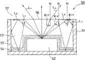
具体来讲,提出了如图6所示的传统半导体发光装置50。Specifically, a conventional semiconductor
在该传统的半导体发光装置中,在具有腔体结构的封装体51的底面上,安装有蓝色LED元件52。该腔体填充有密封树脂,该密封树脂包含透明的热固粘合剂树脂以及散布在其中的混合荧光体。混合荧光体包含红色荧光体和绿色荧光体。因此,蓝色LED元件52被树脂密封。In this conventional semiconductor light emitting device, a
在这种情况下,设计红色荧光体和绿色荧光体,使得红色荧光体和绿色荧光体的特定重力大于粘合剂树脂的特定重力,并且使红色荧光体的中值直径大于绿色荧光体的中值直径。因此,在粘合剂树脂中,红色荧光体的沉降速率大于绿色荧光体的沉降速率。通过在用密封树脂填充之后适当设置足够的沉降时间,可以通过优选地在蓝色LED元件52附近在粘合剂树脂53下部沉淀红色荧光体来形成红色荧光体层54,并且可以通过在红色荧光体层54上方沉淀绿色荧光体,在红色荧光体层54上方形成绿色荧光体层55。In this case, the red phosphor and the green phosphor are designed such that the specific gravity of the red phosphor and the green phosphor is larger than the specific gravity of the binder resin, and the median diameter of the red phosphor is larger than that of the green phosphor. value diameter. Therefore, in the binder resin, the sedimentation rate of the red phosphor is greater than that of the green phosphor. By properly setting a sufficient settling time after filling with the sealing resin, the
因此,通过在用作激发光源的蓝色LED元件52附近设置红色荧光体层54,红色荧光体层54上方的绿色荧光体层52不吸收被来自蓝色LED元件52的蓝光激发的红色荧光体发射的红光,而经受二次激发。该构造还可以提供高亮度发光装置,并且防止发光装置发射的光移向红色波长范围(暖色移,或者移向较长的波长范围)。(参见日本专利申请特开2005-277127号公报)。Therefore, by disposing the
如图6所示,上述的半导体发光装置50设置有基本上平坦的粘合剂树脂53的发光表面56。另外,发光表面56可以形成与半导体发光装置50外部的空气层57的界面,其中,空气层57的折射率低于粘合剂树脂53的折射率。As shown in FIG. 6 , the semiconductor
在该构造中,设置在蓝色LED元件52附近的红色荧光体层54中的红色荧光体被从蓝色LED元件52发射的一部分蓝光激发,从而发射红光。蓝光的剩余部分可以穿过红色荧光体层54,以进入设置在红色荧光体层54上方的绿色荧光体层55。然后,绿色荧光体层55中的绿色荧光体被蓝光的另一部分激发,从而发射绿光。然后,蓝光的剩余部分可以穿过绿色荧光体层55。In this configuration, the red phosphor provided in the
因此,红光、绿光和蓝光的混合光可以被引导穿过粘合剂树脂53而到达发光表面56,并且彼此混合从而产生白光。Accordingly, mixed light of red light, green light, and blue light can be guided through the
到达发光表面56的白光包括光线Lα、光线Lβ和光线Lγ。光线Lα可以相对于发光表面56的法线N以小于临界角τ的角度(交叉角)θ(θ<τ)到达发光表面56,由此被发光表面56折射,从而出射到空气层57。光线Lβ可以以等于临界角τ的角度(交叉角)θ(θ=τ)到达发光表面56,沿着发光表面56前进。The white light reaching the
另外,光线Lγ可以以大于临界角τ的角度(交叉角)θ(θ>τ)到达发光表面56,由此被发光表面56反射(全反射)。然后,光线Lγ可以再次返回到粘合剂树脂53。这就意味着光线Lγ不直接从发光表面56直接出射到空气层57中。In addition, the light ray Lγ may reach the
被光反射表面56全反射并且返回到粘合剂树脂53的光线Lγ可以被导向封装体51的底面,并且被该底面再次反射,从而被导向发光表面56。由此,光线Lγ可以在被发光表面56折射的同时出射到空气层57中。The light Lγ that is totally reflected by the
在这种情况下,在被发光表面56全反射与被封装体51的底面反射之后从发光表面56出射到空气层57之间,光线Lγ可以两次穿过红色荧光体层54和绿色荧光体层55。In this case, after being totally reflected by the light-emitting
于是,光线Lγ中包括的蓝光的量可能由于在反射过程中激发各个荧光体层54和55中的荧光体而减少,并且绿光的量可能由于在穿过红色荧光体层54期间激发红色荧光体(二次激发)而减少,由此红光的量增加。Then, the amount of blue light included in the light Lγ may be reduced due to excitation of the phosphors in the
结果,在被设计用于发射白光的半导体发光装置50中,由于光线Lγ可能被封装体体51的底面反射,因此出射光可能部分地移向红色波长范围(暖色移,或者移向较长的波长范围),造成照明光的色调不均匀。As a result, in the semiconductor
为了防止发光表面的全反射,粘合剂树脂的发光表面可以形成为朝向空气层的凸球面或非球面。然而,在制造方面很难形成用于填充腔体以使得树脂表面具有朝向空气层的凸球面或非球面的树脂。即使可以实现,自动安装机器也难以吸住具有这种表面的半导体发光装置并将其自动安装到布线板上。In order to prevent total reflection of the light-emitting surface, the light-emitting surface of the binder resin may be formed as a convex spherical surface or an aspherical surface toward the air layer. However, it is difficult in terms of manufacturing to form the resin for filling the cavity so that the resin surface has a convex spherical surface or an aspheric surface toward the air layer. Even if it could be realized, it would be difficult for an automatic mounting machine to suck and automatically mount a semiconductor light emitting device having such a surface on a wiring board.
发明内容Contents of the invention
考虑到现有技术的相关问题,本发明的目的在于实现一种半导体发光装置,该半导体发光装置包括:封装体,所述封装体具有腔体;半导体发光元件,所述半导体发光元件安装在所述腔体内;以及密封树脂,所述密封树脂中散布有至少一种波长转换材料,用于密封半导体发光元件。由此构造的半导体发光装置可以在发光表面上投射色调不均匀度较小的白光。In view of the related problems of the prior art, the object of the present invention is to realize a semiconductor light emitting device, which includes: a package, the package has a cavity; a semiconductor light emitting element, the semiconductor light emitting element is installed in the inside the cavity; and a sealing resin, where at least one wavelength conversion material is dispersed in the sealing resin for sealing the semiconductor light-emitting element. The semiconductor light emitting device thus constructed can project white light with less unevenness in color tone on the light emitting surface.
根据本发明的第一方面,提供了一种半导体发光装置,所述半导体发光装置包括:封装体,所述封装体具有包括底面的腔体;半导体发光元件,所述半导体发光元件设置在所述腔体的所述底面上或者与所述腔体的所述底面相邻地设置;第一密封树脂部件,所述第一密封树脂部件包括至少一个波长转换层,所述至少一个波长转换层设置在所述腔体的所述底面附近、在所述半导体发光元件的上方,并包含散布在粘合剂树脂中的诸如荧光体的波长转换材料,并且所述第一密封树脂部件还包括粘合剂树脂层,所述粘合剂树脂层设置在所述波长转换层的上方并主要包含所述粘合剂树脂;以及第二密封树脂部件,所述第二密封树脂部件设置在所述第一密封树脂部件的上方。在该装置中,所述第二密封树脂部件具有顶面,所述顶面被构造为,使得穿过所述半导体发光元件的顶面中心并与所述第二密封树脂部件的所述顶面交叉的直线和所述第二密封树脂部件的所述顶面与所述直线的交叉点处的法线形成一角度,所述角度小于针对来自所述半导体发光元件的所述顶面中心的入射光线的临界角。According to the first aspect of the present invention, there is provided a semiconductor light emitting device, the semiconductor light emitting device includes: a package body, the package body has a cavity including a bottom surface; a semiconductor light emitting element, the semiconductor light emitting element is arranged on the The bottom surface of the cavity is arranged on or adjacent to the bottom surface of the cavity; a first sealing resin part, the first sealing resin part includes at least one wavelength conversion layer, and the at least one wavelength conversion layer is set In the vicinity of the bottom surface of the cavity, above the semiconductor light emitting element, and containing a wavelength conversion material such as a phosphor dispersed in an adhesive resin, and the first sealing resin part further includes an adhesive an adhesive resin layer provided above the wavelength conversion layer and mainly containing the adhesive resin; and a second sealing resin member provided on the first Seal the top of the resin part. In this device, the second sealing resin part has a top surface configured such that it passes through the center of the top surface of the semiconductor light emitting element and is connected to the top surface of the second sealing resin part. The intersecting straight lines and the normal at the intersection point of the top surface of the second encapsulating resin member and the straight lines form an angle smaller than that for the incident light from the center of the top surface of the semiconductor light emitting element. critical angle of light.
在以上第一方面的半导体发光装置中,所述第二密封树脂部件的所述顶面可以是平坦表面、截锥(frustum)表面和三维弯曲表面中的任一种。In the semiconductor light emitting device of the above first aspect, the top surface of the second sealing resin member may be any one of a flat surface, a frustum surface, and a three-dimensionally curved surface.
在以上第一方面和以下方面的半导体发光装置中,通过所述第二树脂密封部件的厚度来调节所述第二密封部件的所述顶面,使得穿过所述半导体发光元件的所述顶面中心并与所述第二密封树脂部件的所述顶面交叉的直线和所述第二二密封树脂部件的所述顶面与所述直线的交叉点处的法线形成所述角度,所述角度小于针对来自所述半导体发光元件的所述顶面中心的入射光线的临界角。In the semiconductor light emitting device of the above first aspect and the following aspect, the top surface of the second sealing member is adjusted by the thickness of the second resin sealing member so that the top surface of the semiconductor light emitting element passes through A straight line at the center of the surface and intersecting the top surface of the second sealing resin part and a normal line at the intersection point of the top surface of the second sealing resin part and the straight line form the angle, so The angle is smaller than a critical angle for incident rays from the center of the top surface of the semiconductor light emitting element.
在以上第一方面和以下方面的半导体发光装置中,所述半导体发光元件是蓝色LED元件,并且所述波长转换层从所述腔体的底面侧起包括红色荧光体层和绿色荧光体层。In the semiconductor light emitting device of the above first aspect and the following aspect, the semiconductor light emitting element is a blue LED element, and the wavelength conversion layer includes a red phosphor layer and a green phosphor layer from the bottom surface side of the cavity .
在以上第一方面和以下方面的半导体发光装置中,所述半导体发光元件是紫外LED元件,并且所述波长转换层从所述腔体的底面侧起包括红色荧光体层、绿色荧光体层和蓝色荧光体层。In the semiconductor light emitting device of the above first aspect and the following aspect, the semiconductor light emitting element is an ultraviolet LED element, and the wavelength conversion layer includes a red phosphor layer, a green phosphor layer and blue phosphor layer.
本发明的半导体发光装置包括所述至少一个波长转换层(荧光体层),所述至少一个波长转换层位于安装在所述腔体的所述底面附近的所述半导体发光元件的上方;以及位于所述波长转换层上方的包括所述粘合剂树脂层和所述第二密封树脂部件的两个不同密封树脂部件。另外,本发明的半导体发光装置是如下构造的:所述第二密封树脂部件(上树脂层)的所述顶面被设计为,穿过所述半导体发光元件的所述顶面中心并与所述第二密封树脂部件的所述顶面交叉的直线和所述第二密封树脂部件的所述顶面与所述直线的交叉点处的法线形成一角度,所述角度小于针对来自树脂层的入射光线的临界角。The semiconductor light-emitting device of the present invention includes the at least one wavelength conversion layer (phosphor layer), the at least one wavelength conversion layer is located above the semiconductor light-emitting element installed near the bottom surface of the cavity; and Two different sealing resin parts including the adhesive resin layer and the second sealing resin part above the wavelength conversion layer. In addition, the semiconductor light-emitting device of the present invention is structured as follows: the top surface of the second sealing resin member (upper resin layer) is designed to pass through the center of the top surface of the semiconductor light-emitting element and to be in contact with the The straight line intersecting the top surface of the second sealing resin part and the normal line at the intersection point of the top surface of the second sealing resin part and the straight line form an angle smaller than the The critical angle of the incident ray.
在如上构造的半导体发光装置中,防止了第二密封树脂部件的顶面反射从半导体发光元件发射并到达用作发光表面的第二密封树脂部件的顶面的光、以及从被来自半导体发光元件的光激发的波长转换材料发射并到达第二密封树脂部件的顶面的光。In the semiconductor light emitting device configured as above, the top surface of the second sealing resin member is prevented from reflecting light emitted from the semiconductor light emitting element and reaching the top surface of the second sealing resin member serving as the light emitting surface, and light being transmitted from the semiconductor light emitting element. The light excited by the wavelength converting material emits and reaches the top surface of the second sealing resin member.
因此,由于可以防止光被第一密封树脂部件的顶面和第二密封树脂部件的顶面二者全反射,从而减少了波长转换材料的二次激发的出现,因此从该半导体发光装置投射的光可以是白光,而没有色移和色调不均匀。Therefore, since light can be prevented from being totally reflected by both the top surface of the first sealing resin part and the top surface of the second sealing resin part, thereby reducing the occurrence of secondary excitation of the wavelength conversion material, the light projected from the semiconductor light emitting device The light can be white without color shift and unevenness in tone.
另外,从半导体发光装置投射的光不会部分地移向红色波长范围(暖色移,或者移向较长的波长范围),得到发光表面上方的照明光的均匀色调。In addition, the light projected from the semiconductor light emitting device is not partially shifted to the red wavelength range (warm shift, or shifted to a longer wavelength range), resulting in a uniform color tone of the illumination light above the light emitting surface.
附图说明Description of drawings
图1是示出根据本发明的第一示例性实施方式的半导体发光装置的剖面图;1 is a cross-sectional view illustrating a semiconductor light emitting device according to a first exemplary embodiment of the present invention;
图2是示出根据本发明的第二示例性实施方式的半导体发光装置的剖面图;2 is a cross-sectional view illustrating a semiconductor light emitting device according to a second exemplary embodiment of the present invention;
图3是示出根据本发明的第二示例性实施方式的半导体发光装置的变型例的剖面图;3 is a cross-sectional view illustrating a modified example of the semiconductor light emitting device according to the second exemplary embodiment of the present invention;
图4是示出根据本发明的第三示例性实施方式的半导体发光装置的剖面图;4 is a cross-sectional view illustrating a semiconductor light emitting device according to a third exemplary embodiment of the present invention;
图5是示出根据本发明的第三示例性实施方式的半导体发光装置的剖面图;以及5 is a cross-sectional view showing a semiconductor light emitting device according to a third exemplary embodiment of the present invention; and
图6是示出传统半导体发光装置的剖面图。FIG. 6 is a cross-sectional view showing a conventional semiconductor light emitting device.
具体实施方式Detailed ways
下文中,将参照附图描述本发明的一些优选示例性实施方式。在描述中,用相同的参考标号表示相同或类似的组件。应该注意的是,下面的示例性实施方式受各种技术上的优选特征的限制,但是本发明的范围不限于此。Hereinafter, some preferred exemplary embodiments of the present invention will be described with reference to the accompanying drawings. In the description, the same or similar components are denoted by the same reference numerals. It should be noted that the following exemplary embodiments are limited by various technically preferable features, but the scope of the present invention is not limited thereto.
[第一示例性实施方式][First Exemplary Embodiment]
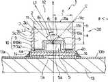
图1是示出根据本发明第一示例性实施方式的半导体发光装置的剖面图。FIG. 1 is a cross-sectional view illustrating a semiconductor light emitting device according to a first exemplary embodiment of the present invention.
本示例性实施方式的半导体发光装置30包括具有腔体2和底部3a的封装体3。多个导电图案4a和4b以如下方式分开地单独设置在底部3a的上表面上:它们延伸到底部3a的背面,同时穿透封装体3。在该示例性实施方式中,封装体3可以由诸如玻璃环氧树脂的树脂材料形成。The semiconductor
蓝色LED元件5设置在封装体3的底部3a的上表面上的导电图案4a上,其间设置了导电粘合部件(未示出)。蓝色LED元件(下文中,简称为“LED元件”)可以用作半导体发光元件,它作为光源以发射蓝光。LED元件5具有下电极(未示出),该下电极经由导电粘合部件电连接到导电图案4a。LED元件5具有上电极(未示出),该上电极经由接合导线6电连接到导电图案4b,由此在LED元件5的上电极与导电图案4b之间实现电连接。The
应该注意的是,LED元件不限于如上所述利用接合导线在电极与导电图案之间建立连接的类型,而是可以是利用凸点电极的倒装芯片型。It should be noted that the LED element is not limited to the type that establishes connection between the electrode and the conductive pattern using bonding wires as described above, but may be a flip chip type using bump electrodes.
在设置有LED元件5的腔体2的下部中,填充有第一密封树脂部件10。可以通过将包含两种荧光体(红色荧光体7a和绿色荧光体8a)的波长转换材料散布在透明的热固粘合剂树脂9中,来制备第一密封树脂部件10。可以通过激发光来激发红色荧光体7a,从而发射红光(波长转换)。可以通过激发光来激发绿色荧光体8a,从而发射绿光(波长转换)。在本示例性实施方式中,第一密封树脂部件10可以具有平坦的顶面10a。In the lower portion of the
在第一密封树脂部件10中,通过在用密封树脂部件填充之后适当设置足够的沉降时间,可以通过优选地在粘合剂树脂9的下部在LED元件5附近沉淀红色荧光体7a来形成红色荧光体层7,并且可以通过在红色荧光体层7的上方沉淀绿色荧光体8a来在红色荧光体层7上方形成绿色荧光体层8。In the first sealing resin part 10, by appropriately setting a sufficient settling time after filling with the sealing resin part, red fluorescent light can be formed by precipitating the
这意味着,包含发射波长较长的荧光体的荧光体层沉淀得更靠近光源侧。这可以通过各种方式实现,如在以上背景技术部分所讨论的,可以通过调节沉降速率,使得发射波长较长的光的荧光体的中值直径大于发射波长较短的光的荧光体的中值直径,从而控制沉淀顺序。This means that a phosphor layer containing a phosphor having a longer emission wavelength is deposited closer to the light source side. This can be achieved in various ways, as discussed in the background section above, by adjusting the sedimentation rate such that the median diameter of phosphors emitting longer wavelength light is larger than the median diameter of phosphors emitting light of shorter wavelength. Value diameter, thus controlling the precipitation order.
在腔体2内在第一密封树脂部件10的上方,设置有包含透明树脂材料的第二密封树脂部件11。构造第二密封树脂部件11,使得顶面11a被形成为平坦的并且位于封装体3的侧壁3b的上边缘3d上方。Inside the
第一密封树脂部件10的粘合剂树脂9和第二密封树脂部件11的透明树脂材料可以彼此相同或不同。考虑到要防止由于热膨胀系数差异而导致第一密封树脂部件10和第二密封树脂部件11的界面剥离并且要防止它们之间界面处的全反射或折射,它们优选地为相同的树脂材料。The
树脂材料的示例包括硅树脂、环氧树脂等。优选的是硅树脂,这是因为,当LED元件5点亮时,LED元件5附近的由硅树脂制成的粘合剂树脂9受到的由于树脂热膨胀导致的应力的影响较小。Examples of resin materials include silicone resin, epoxy resin, and the like. Silicone is preferable because, when the
此外,当第一密封树脂部件10的折射率和第二密封树脂部件11的折射率是n并且与第二密封树脂部件11的顶面11a接触的空气层12的折射率为1时,来自第二密封树脂部件11的入射光在空气层12上的临界角τ可以用关系式τ=sin-1(1/n)表示。Furthermore, when the refractive index of the first sealing resin member 10 and the refractive index of the second
另外,假设从LED元件5的顶面5a(主发光表面)到第一密封树脂部件10的顶面10a的距离为a,第二密封树脂部件11的厚度为b,并且从光轴X与顶面11a交叉的点到顶面11a的外周11c的距离为c。在这种情况下,构造本发明的半导体发光装置,使得a、b、c和τ之间的关系满足τ>tan-1(c/(a+b))。In addition, assuming that the distance from the
换言之,当光轴X垂直于第二密封树脂部件11的顶面11a时,可以设置a、b和c,使得穿过LED元件5的顶面5a的中心并与第二密封树脂部件11的顶面11a的外周11c交叉的直线C和穿过LED元件5的顶面5a的中心的光轴X(相当于第二密封树脂部件11的顶面11a与所述直线的交叉点处的法线)形成角度θ,该角度θ小于临界角τ(θ<τ)。In other words, when the optical axis X is perpendicular to the
因此,第二密封树脂部件11的顶面11a的形状不限于特定形状,只要a、b、c和τ之间的关系得以满足即可,并且该形状可以是矩形或圆形的形状。当顶面11a是圆形时,顶面11a是如下的圆形:半径为c并且中心位于LED元件5的光轴X上。Therefore, the shape of the
在本示例性实施方式中,第一密封树脂部件10的顶面10a的形状可以与第二密封树脂部件11的下表面11b的形状相同,使得它们彼此完全重叠地形成界面。另外,该界面和第二密封树脂部件11的顶面11a优选地具有相同的形状。In the present exemplary embodiment, the shape of the
封装体3具有用于形成腔体2的侧壁3b,用第一密封树脂部件10和第二密封树脂部件11填充腔体2,并且侧壁3b的内表面3c优选地形成圆柱形,或者在LED元件5的照明方向上包括沿着背离LED元件5的方向开口更宽的连续倾斜表面。The package body 3 has a side wall 3b for forming a
可以通过浇注模制(potting molding)方法将用于第一密封树脂部件10和第二密封树脂部件11的树脂材料填充到腔体2中。在一个常规工序中,将用于第一密封树脂部件10的树脂材料填充到腔体2中,并且在室温下固化,随后将用于第二密封树脂部件11的树脂材料散布到封装体3内的固化后的第一密封树脂部件10上,并且在室温下固化。这可以形成具有平坦的顶面11a的第二密封树脂部件11。平坦的顶面11a可以被自动安装机械吸住以安装到布线板上,由此提高了制造效率。The resin material for the first sealing resin part 10 and the second
然后,从封装体3延伸的导电图案4a和4b可以通过诸如焊料的导电连接部件14电连接到在布线板13上方形成的电路图案13a和13b。以此方式,可以将由此制备出的半导体发光装置30固定并且电连接到布线板13,从而完成半导体发光模块1。Then, the
当本示例性实施方式的半导体发光模块1点亮时,从LED元件5向第二密封树脂部件11的顶面11a发射的光线L1可以按顺序穿过第一密封树脂部件10的红色荧光体层7、绿色荧光体层8和粘合剂树脂层9以及第二密封树脂部件11,从而到达第二密封树脂部件11的顶面11a。When the semiconductor light emitting module 1 of this exemplary embodiment is turned on, the light L1 emitted from the
到达第二密封树脂部件11的顶面11a的光线L1可以以小于针对顶面11a的临界角τ的角θL入射到顶面11a上。因此,几乎全部的到达顶面11a的光线L1都可以出射到空气层12,而没有被顶面11a全反射。The light L1 reaching the
从LED元件5发射的另一光线L2可以按顺序穿过第一密封树脂部件10的红色荧光体层7、绿色荧光体层8和粘合剂树脂层9、以及第二密封树脂部件11,从而到达第二密封树脂部件11的侧面。然后,光线L2可以被侧面全反射,从而到达顶面11a并且出射到空气层12。Another light L2 emitted from the
换言之,几乎全部的从LED元件5发射并导向第二密封树脂部件11的光都可以只穿过红色荧光体层17和绿色荧光体层18一次,这意味着可以防止蓝光的光量降低以及由来自绿色荧光体层8的绿光导致红色荧光体的二次激发。In other words, almost all of the light emitted from the
结果,从半导体发光模块1投射的光不会部分地移向红色波长范围(暖色移,或移向较长波长范围),得到发光表面上方的白色照明光的均匀色调。As a result, the light projected from the semiconductor light emitting module 1 is not partially shifted to the red wavelength range (warm shift, or shifted to a longer wavelength range), resulting in a uniform tone of white illumination light above the light emitting surface.
[第二示例性实施方式][Second Exemplary Embodiment]
图2是根据本发明第二示例性实施方式的半导体发光装置的剖面图。2 is a cross-sectional view of a semiconductor light emitting device according to a second exemplary embodiment of the present invention.
所示出的本示例性实施方式的半导体发光装置30与第一示例性实施方式的不同之处在于,其中从LED元件发射并且到达的光可以出射到空气层而不发生任何全反射的第二密封树脂部件的顶面的面积扩大为比第一示例性实施方式中的面积大。The semiconductor
与第一示例性实施方式一样,该构造可以使得在发光表面实现具有均匀色调的白色照明光,并且,由于比第一示例性实施方式更大地扩大了照明区域,所以可以提高光利用效率。Like the first exemplary embodiment, this configuration can realize white illumination light with a uniform tone on the light emitting surface, and since the illumination area is enlarged more than that of the first exemplary embodiment, light utilization efficiency can be improved.
具体来讲,第一密封树脂部件10的顶面10a被形成为平坦的,并且被设置成与封装体3的侧壁3b的上边缘3d齐平。另外,设置在第一密封树脂部件10上的第二密封树脂部件11的顶面11a包括与光轴X交叉的平坦部分11d、以及包围平坦部分11d并向着封装体3的上边缘3d倾斜的倾斜部分11f。Specifically, the
在本示例性实施方式中,假设第一密封树脂部件10的折射率和设置在第一密封树脂部件10上方的第二密封树脂部件11的折射率为n,与第二密封树脂部件11的顶面11a接触的空气层12的折射率为1,从LED元件5的顶面5a(主发光表面)到第一密封树脂部件10的顶面10a的距离为a,从第二密封树脂部件11的下表面11b到平坦部分11d的距离为b,并且从光轴X与顶面11a交叉的点到平坦部分11d的外周11e的距离为c。在这种情况下,设计平坦部分11d,使得a、b、c和τ之间的关系满足τ>tan-1(c/(a+b))。In the present exemplary embodiment, it is assumed that the refractive index of the first sealing resin member 10 and the refractive index of the second
换言之,当光轴X垂直于第二密封树脂部件11的顶面11a时,可以设置a、b和c,使得穿过LED元件5的顶面5a的中心并与第二密封树脂部件11的平坦部分11d的外周11e交叉的直线C和穿过LED元件5的顶面5a的中心的光轴X(相当于第二密封树脂部件11的顶面11a与直线的交叉点处的法线)形成角度θ1,该角度θ1小于临界角τ(θ<τ)。In other words, when the optical axis X is perpendicular to the
因此,第二密封树脂部件11的平坦部分11d的形状不限于特定形状,只要a、b、c和τ之间的关系得以满足即可,并且该形状可以是矩形或圆形的形状。当平坦部分11d是圆形时,平坦部分11d是如下的圆形:半径为c并且中心位于LED元件5的光轴X上。Therefore, the shape of the flat portion 11d of the second
另外,倾斜部分11f形成为连续倾斜的表面,其上边缘是平坦部分11d的外周11e,下边缘是封装体3的侧壁3b的上边缘3d。然后,倾斜部分11f是按如下方式设计的:使得穿过LED元件5的顶面5a的中心并与第二密封树脂部件11的倾斜部分11f交叉的直线D和倾斜表面11f与直线D的交叉点处的法线N1形成角度θ2,该角度θ2小于临界角τ(θ2<τ)。In addition, the inclined portion 11f is formed as a continuously inclined surface whose upper edge is the outer periphery 11e of the flat portion 11d and whose lower edge is the upper edge 3d of the side wall 3b of the package body 3 . Then, the inclined portion 11f is designed in such a manner that the straight line D passing through the center of the
通过浇注模制方法将用于第一密封树脂部件10的树脂材料填充到腔体2中,在室温下固化,然后,可以通过金属模制在封装体3内在固化后的第一密封树脂部件10上形成第二密封树脂部件11。另选的是,第二密封树脂部件11可以由相同的树脂材料单独形成为具有预定形状,由此形成的第二密封树脂部件11可以粘附于第一密封树脂部件10,以插入在其间的相同树脂材料作为粘合剂。The resin material for the first sealing resin part 10 is filled into the
当具有本示例性实施方式的以上构造的半导体发光装置30点亮时,从LED元件5向着第二密封树脂部件11的平坦部分11d发射的光线L1可以按顺序穿过第一密封树脂部件10的红色荧光体层7、绿色荧光体层8、粘合剂树脂层9以及第二密封树脂部件11,从而到达第二密封树脂部件11的平坦部分11d。When the semiconductor
到达第二密封树脂部件11的平坦部分11d的光线L1可以以小于针对平坦部分11d的临界角τ的角度θL1入射到平坦部分11d上。因此,几乎全部的到达平坦部分11d的光线L都可以出射到空气层12,而不被平坦部分11d全反射。The light ray L1 reaching the flat portion 11d of the second
因此,几乎全部的从LED元件5发射并导向第二密封树脂部件11的平坦部分11d的光都可以只穿过红色荧光体层7和绿色荧光体层8一次,这意味着,可以防止蓝光的光量降低以及由来自绿色荧光体层8的绿光而导致红色荧光体的二次激发。Therefore, almost all of the light emitted from the
另一方向,从LED元件5向着第二密封树脂部件11的倾斜部分11f发射的光线L2可以按顺序穿过第一密封树脂部件10的红色荧光体层7、绿色荧光体层8和粘合剂树脂层9、以及第二密封树脂部件11,从而到达第二密封树脂部件11的倾斜部分11f。In the other direction, light L2 emitted from the
到达第二密封树脂部件11的倾斜部分11f的光线L2可以以小于针对倾斜部分11f的法线N2的临界角τ的角度θL2入射到倾斜部分11f上。因此,几乎全部的到达倾斜部分11f的光线L都可以出射到空气层12,而不被倾斜部分11f全反射。The ray L2 reaching the inclined portion 11f of the second
因此,几乎全部的从LED元件5发射并导向第二密封树脂部件11的倾斜部分11f的光都可以只穿过红色荧光体层7和绿色荧光体层8一次,这意味着,可以防止蓝光的光量降低以及由来自绿色荧光体层8的绿光而导致红色荧光体的二次激发。Therefore, almost all of the light emitted from the
结果,从半导体发光装置30的第二密封树脂部件11的顶面11a(包括平坦部分11d和倾斜部分11f)投射的光不会部分地移向红色波长范围(暖色移或者移向较长波长范围),得到在发光表面上方的白色照明光的均匀色调。As a result, the light projected from the
此外,半导体发光装置30(或模块1)可以由其它制造方法来形成。例如,通过浇注模制方法将第一密封树脂部件10形成在腔体2内,并且在室温下固化。然后,可以将封装体3安装在布线板13上。此后,可以通过液体散布器等将用于第二密封树脂部件11的树脂材料散布在第一密封树脂部件10上,并且在室温下固化,从而完成半导体发光装置30(或模块1)。In addition, the semiconductor light emitting device 30 (or the module 1 ) may be formed by other manufacturing methods. For example, the first sealing resin part 10 is formed in the
在这种情况下,如作为变型例的图3所示,第二密封树脂部件11的顶面11g可以是凸曲面而不是第二示例性实施方式中的平坦部分11d和倾斜部分11f。与第二示例性实施方式的平坦部分11d相比,凸顶面11g难以对到达的光进行全反射。因此,第二密封树脂部件11的顶面11g的光学性能优于第二示例性实施方式的第二密封树脂部件11的平坦部分11d。In this case, as shown in FIG. 3 as a modification, the
变型例的第二密封树脂部件11具有弯曲部分11h,弯曲部分11h基本上对应于第二示例性实施方式的第二密封树脂部件11的平坦部分11d的外周11e,并且弯曲部分11h被形成为略微弧形的(不是急剧弯曲)。与第二示例性实施方式的平坦部分11d的外周11e的环绕区域相比,弧形的弯曲部分11h难以对到达的光进行全反射。因此,第二密封树脂部件11的弯曲部分11h的光学性能优于第二示例性实施方式的第二密封部件11的平坦部分11d。The second
变型例的第二密封树脂部件11具有倾斜部分11i,该倾斜部分11i基本上对应于第二示例性实施方式的第二密封树脂部件11的倾斜部分11f,并且,与第二示例性实施方式相比,倾斜部分11i形成得稍微更凸出些。与具有直线剖面的第二示例性实施方式的倾斜部分11f相比,倾斜部分11i难以对到达的光进行全反射。因此,第二密封树脂部件11的倾斜部分11i的光学性能优于第二示例性实施方式的第二密封树脂部件11的倾斜部分11f。The second
[第三示例性实施方式][Third Exemplary Embodiment]
图4和图5是示出根据本发明的第三示例性实施方式的半导体发光装置的剖面图。4 and 5 are cross-sectional views illustrating a semiconductor light emitting device according to a third exemplary embodiment of the present invention.
本示例性实施方式的半导体发光装置30的基本结构与第一示例性实施方式的基本结构相同,其中,半导体发光装置30在腔体2内包括第一密封树脂部件10和第二密封树脂部件11以密封LED元件5,并且安装在布线板13上,不同之处在于,整个装置30覆盖有例如由树脂材料制成的透镜21,从而完成半导体发光模块20。The basic structure of the semiconductor
参照图4,假设第一密封树脂部件10(粘合剂树脂层9)的折射率和设置在第一密封树脂部件10上的第二密封树脂部件11的折射率为n,并且与第二密封树脂部件11接触的树脂透镜21的折射率为n2。在这种情况下,当n2等于或大于n1(n1≤n2)时,从内部到达第二密封树脂部件11的顶面11a的光线L1可以进入树脂透镜21,而不被顶面11a全反射。因此,当从LED元件5的顶面5a(主发光表面)到第一密封树脂部件10的顶面10a的距离为a、第二密封树脂部件11的厚度为b、并且从光轴X与顶面11a交叉的点到顶面11a的外周11c的距离为c时,可以将a、b和c自由设置为任意的值(图4示出了n1<n2的情况)。Referring to Fig. 4, assume that the refractive index of the first sealing resin member 10 (adhesive resin layer 9) and the refractive index of the second
另一方面,当折射率n2小于折射率n1时,从第二密封树脂部件11进入树脂透镜21的光的临界角τ可以用τ=sin-1(n2/n1)表示。因此,在这种情况下,构造半导体发光装置,使得a、b、c和τ之间的关系满足τ>tan-1(c/(a+b))。On the other hand, when the refractive index n2 is smaller than the refractive index n1, the critical angle τ of light entering the
换言之,由于光轴X垂直于第二密封树脂部件11的顶面11a,因此可以设置a、b和c,使得穿过LED元件5的顶面5a的中心并与第二密封树脂部件11的顶面11a的外周11c交叉的直线C和穿过LED元件5的顶面5a的中心的光轴X(相当于第二密封树脂部件11的顶面11a与所述直线的交叉点处的法线)形成角度θ,该角度θ小于临界角τ(θ<τ)。In other words, since the optical axis X is perpendicular to the
当本示例性实施方式的半导体发光模块20点亮时,从LED元件5向着第二密封树脂部件11的顶面11a发射的光线L可以按顺序穿过第一密封树脂部件10的红色荧光体层7、绿色荧光体层8和粘合剂树脂层9、以及第二密封树脂部件11,从而到达第二密封树脂部件11的顶面11a。When the semiconductor
到达第二密封树脂部件11的顶面11a的光线L可以以小于针对顶面11a的临界角τ的θL入射到顶面11a上。因此,几乎全部的到达顶面11a的光线L都可以进入树脂透镜21,而不被顶面11a全反射。The light rays L reaching the
进入树脂透镜21的光线L可以被引导穿过树脂透镜21并且到达光输出表面21a,该光输出表面21a被形成为基本球形,从而覆盖作为光源的LED元件5。因此,到达光输出表面21a的光线L可以出射到空气层12,而不出现全反射。The light rays L entering the
换言之,几乎全部的从LED元件5发射并导向第二密封树脂部件11的光可以只穿过红色荧光体层7和绿色荧光体层8一次,这意味着,可以防止蓝光的光量降低以及由来自绿色荧光体层8的绿光而导致红色荧光体的二次激发。In other words, almost all of the light emitted from the
结果,从半导体发光模块20经过树脂透镜21投射的光不会部分地移向红色波长范围(暖色移,或者移向较长波长范围),得到在发光表面上方的白色照明光的均匀色调。As a result, the light projected from the semiconductor
此外,以上示例性实施方式处理了以下情况:蓝色LED元件用作光源,并且包含红色荧光体和绿色荧光体的混合荧光体用作提供伪白光(pseudo white light)的波长转换材料。然而,本发明不限于这些特定模式。如现有技术部分所讨论的,例如,紫外LED元件可以用作光源,并且包含蓝色荧光体、红色荧光体和绿色荧光体的混合荧光体可以用于产生伪白光。Furthermore, the above exemplary embodiments deal with the case where a blue LED element is used as a light source, and a mixed phosphor including a red phosphor and a green phosphor is used as a wavelength conversion material that provides pseudo white light. However, the present invention is not limited to these specific modes. As discussed in the prior art section, for example, ultraviolet LED elements can be used as light sources, and hybrid phosphors containing blue, red, and green phosphors can be used to generate pseudo-white light.
在这种情况下,各个荧光体层可以沉淀在腔体内,使得包含发射波长较长的荧光体的荧光体层沉淀得更靠近光源侧,以防止任何的二次激发和三次激发。具体来讲,荧光体层可以是从光源侧开始按顺序沉淀的红色荧光体层、绿色荧光体层和蓝色荧光体层。In this case, the respective phosphor layers may be deposited in the cavity such that the phosphor layer containing the phosphor with longer emission wavelength is deposited closer to the light source side to prevent any secondary excitation and tertiary excitation. Specifically, the phosphor layer may be a red phosphor layer, a green phosphor layer, and a blue phosphor layer deposited sequentially from the light source side.
在另一个实施方式中,蓝色LED元件可以结合黄色荧光体(其可以被蓝光激发以发射黄光)来用作光源,由此提供伪白光。在这种情况下,本发明可以防止以上构造导致的二次激发,从而提供颜色不均匀度减小的发光表面。In another embodiment, a blue LED element can be used as a light source in combination with a yellow phosphor (which can be excited by blue light to emit yellow light), thereby providing pseudo-white light. In this case, the present invention can prevent secondary excitation caused by the above configuration, thereby providing a light emitting surface with reduced color unevenness.
Claims (5)
Applications Claiming Priority (2)
| Application Number | Priority Date | Filing Date | Title |
|---|---|---|---|
| JP2009023898AJP2010182809A (en) | 2009-02-04 | 2009-02-04 | Semiconductor light-emitting apparatus |
| JP2009-023898 | 2009-02-04 |
Publications (2)
| Publication Number | Publication Date |
|---|---|
| CN101800281Atrue CN101800281A (en) | 2010-08-11 |
| CN101800281B CN101800281B (en) | 2014-09-17 |
Family
ID=42595854
Family Applications (1)
| Application Number | Title | Priority Date | Filing Date |
|---|---|---|---|
| CN201010112923.8AExpired - Fee RelatedCN101800281B (en) | 2009-02-04 | 2010-02-04 | Semiconductor light emitting device |
Country Status (2)
| Country | Link |
|---|---|
| JP (1) | JP2010182809A (en) |
| CN (1) | CN101800281B (en) |
Cited By (32)
| Publication number | Priority date | Publication date | Assignee | Title |
|---|---|---|---|---|
| CN104157769A (en)* | 2013-05-13 | 2014-11-19 | 新世纪光电股份有限公司 | Light-emitting diode packaging structure |
| CN105122015A (en)* | 2013-04-11 | 2015-12-02 | 株式会社电装 | Vehicle display device |
| CN105308419A (en)* | 2013-07-30 | 2016-02-03 | 株式会社电装 | Display apparatus |
| US9640347B2 (en) | 2013-09-30 | 2017-05-02 | Apple Inc. | Keycaps with reduced thickness |
| US9704670B2 (en) | 2013-09-30 | 2017-07-11 | Apple Inc. | Keycaps having reduced thickness |
| US9704665B2 (en) | 2014-05-19 | 2017-07-11 | Apple Inc. | Backlit keyboard including reflective component |
| US9710069B2 (en) | 2012-10-30 | 2017-07-18 | Apple Inc. | Flexible printed circuit having flex tails upon which keyboard keycaps are coupled |
| US9715978B2 (en) | 2014-05-27 | 2017-07-25 | Apple Inc. | Low travel switch assembly |
| US9761389B2 (en) | 2012-10-30 | 2017-09-12 | Apple Inc. | Low-travel key mechanisms with butterfly hinges |
| US9779889B2 (en) | 2014-03-24 | 2017-10-03 | Apple Inc. | Scissor mechanism features for a keyboard |
| US9793066B1 (en) | 2014-01-31 | 2017-10-17 | Apple Inc. | Keyboard hinge mechanism |
| US9870880B2 (en) | 2014-09-30 | 2018-01-16 | Apple Inc. | Dome switch and switch housing for keyboard assembly |
| CN107768507A (en)* | 2016-08-17 | 2018-03-06 | 晶元光电股份有限公司 | Light emitting device and method for manufacturing the same |
| US9908310B2 (en) | 2013-07-10 | 2018-03-06 | Apple Inc. | Electronic device with a reduced friction surface |
| US9916945B2 (en) | 2012-10-30 | 2018-03-13 | Apple Inc. | Low-travel key mechanisms using butterfly hinges |
| US9927895B2 (en) | 2013-02-06 | 2018-03-27 | Apple Inc. | Input/output device with a dynamically adjustable appearance and function |
| US9934915B2 (en) | 2015-06-10 | 2018-04-03 | Apple Inc. | Reduced layer keyboard stack-up |
| CN107887490A (en)* | 2016-09-30 | 2018-04-06 | 日亚化学工业株式会社 | Light-emitting device |
| US9971084B2 (en) | 2015-09-28 | 2018-05-15 | Apple Inc. | Illumination structure for uniform illumination of keys |
| US9997308B2 (en) | 2015-05-13 | 2018-06-12 | Apple Inc. | Low-travel key mechanism for an input device |
| US9997304B2 (en) | 2015-05-13 | 2018-06-12 | Apple Inc. | Uniform illumination of keys |
| US10082880B1 (en) | 2014-08-28 | 2018-09-25 | Apple Inc. | System level features of a keyboard |
| US10083805B2 (en) | 2015-05-13 | 2018-09-25 | Apple Inc. | Keyboard for electronic device |
| US10115544B2 (en) | 2016-08-08 | 2018-10-30 | Apple Inc. | Singulated keyboard assemblies and methods for assembling a keyboard |
| US10128064B2 (en) | 2015-05-13 | 2018-11-13 | Apple Inc. | Keyboard assemblies having reduced thicknesses and method of forming keyboard assemblies |
| US10262814B2 (en) | 2013-05-27 | 2019-04-16 | Apple Inc. | Low travel switch assembly |
| US10353485B1 (en) | 2016-07-27 | 2019-07-16 | Apple Inc. | Multifunction input device with an embedded capacitive sensing layer |
| US10755877B1 (en) | 2016-08-29 | 2020-08-25 | Apple Inc. | Keyboard for an electronic device |
| US10775850B2 (en) | 2017-07-26 | 2020-09-15 | Apple Inc. | Computer with keyboard |
| US10796863B2 (en) | 2014-08-15 | 2020-10-06 | Apple Inc. | Fabric keyboard |
| US11500538B2 (en) | 2016-09-13 | 2022-11-15 | Apple Inc. | Keyless keyboard with force sensing and haptic feedback |
| CN115735081A (en)* | 2020-06-29 | 2023-03-03 | 西铁城电子株式会社 | Light emitting device |
Families Citing this family (5)
| Publication number | Priority date | Publication date | Assignee | Title |
|---|---|---|---|---|
| JP2013004734A (en)* | 2011-06-16 | 2013-01-07 | Asahi Glass Co Ltd | Light-emitting device |
| KR102076243B1 (en)* | 2013-09-04 | 2020-02-12 | 엘지이노텍 주식회사 | A light emitting device package |
| JP6896038B2 (en)* | 2015-05-12 | 2021-06-30 | 三菱電機株式会社 | Display device |
| KR20180125639A (en)* | 2016-06-27 | 2018-11-26 | (주)라이타이저코리아 | Package for Light Emitting Device |
| JP7226789B2 (en)* | 2019-05-10 | 2023-02-21 | 国立研究開発法人物質・材料研究機構 | light emitting device |
Citations (3)
| Publication number | Priority date | Publication date | Assignee | Title |
|---|---|---|---|---|
| CN1661825A (en)* | 2004-02-26 | 2005-08-31 | 京瓷株式会社 | Lighting devices and lighting devices |
| JP2007116124A (en)* | 2005-09-20 | 2007-05-10 | Matsushita Electric Works Ltd | Light emitting device |
| CN101081980A (en)* | 2006-06-02 | 2007-12-05 | 夏普株式会社 | Wavelength conversion member and light-emitting device |
Family Cites Families (5)
| Publication number | Priority date | Publication date | Assignee | Title |
|---|---|---|---|---|
| JP2001077425A (en)* | 1999-08-31 | 2001-03-23 | Yoshinobu Suehiro | Light-emitting element |
| JP3230518B2 (en)* | 1999-10-19 | 2001-11-19 | サンケン電気株式会社 | Semiconductor light emitting device |
| JP2005197423A (en)* | 2004-01-07 | 2005-07-21 | Matsushita Electric Ind Co Ltd | LED light source |
| JP4451178B2 (en)* | 2004-03-25 | 2010-04-14 | スタンレー電気株式会社 | Light emitting device |
| JP4453553B2 (en)* | 2005-01-14 | 2010-04-21 | パナソニック電工株式会社 | Light source device and illumination device |
- 2009
- 2009-02-04JPJP2009023898Apatent/JP2010182809A/enactivePending
- 2010
- 2010-02-04CNCN201010112923.8Apatent/CN101800281B/ennot_activeExpired - Fee Related
Patent Citations (3)
| Publication number | Priority date | Publication date | Assignee | Title |
|---|---|---|---|---|
| CN1661825A (en)* | 2004-02-26 | 2005-08-31 | 京瓷株式会社 | Lighting devices and lighting devices |
| JP2007116124A (en)* | 2005-09-20 | 2007-05-10 | Matsushita Electric Works Ltd | Light emitting device |
| CN101081980A (en)* | 2006-06-02 | 2007-12-05 | 夏普株式会社 | Wavelength conversion member and light-emitting device |
Cited By (55)
| Publication number | Priority date | Publication date | Assignee | Title |
|---|---|---|---|---|
| US9761389B2 (en) | 2012-10-30 | 2017-09-12 | Apple Inc. | Low-travel key mechanisms with butterfly hinges |
| US9916945B2 (en) | 2012-10-30 | 2018-03-13 | Apple Inc. | Low-travel key mechanisms using butterfly hinges |
| US10211008B2 (en) | 2012-10-30 | 2019-02-19 | Apple Inc. | Low-travel key mechanisms using butterfly hinges |
| US11023081B2 (en) | 2012-10-30 | 2021-06-01 | Apple Inc. | Multi-functional keyboard assemblies |
| US10254851B2 (en) | 2012-10-30 | 2019-04-09 | Apple Inc. | Keyboard key employing a capacitive sensor and dome |
| US9710069B2 (en) | 2012-10-30 | 2017-07-18 | Apple Inc. | Flexible printed circuit having flex tails upon which keyboard keycaps are coupled |
| US10699856B2 (en) | 2012-10-30 | 2020-06-30 | Apple Inc. | Low-travel key mechanisms using butterfly hinges |
| US9927895B2 (en) | 2013-02-06 | 2018-03-27 | Apple Inc. | Input/output device with a dynamically adjustable appearance and function |
| US10114489B2 (en) | 2013-02-06 | 2018-10-30 | Apple Inc. | Input/output device with a dynamically adjustable appearance and function |
| CN105122015A (en)* | 2013-04-11 | 2015-12-02 | 株式会社电装 | Vehicle display device |
| CN105122015B (en)* | 2013-04-11 | 2017-03-15 | 株式会社电装 | Display apparatus |
| CN104157769B (en)* | 2013-05-13 | 2017-04-05 | 新世纪光电股份有限公司 | Light-emitting diode packaging structure |
| CN104157769A (en)* | 2013-05-13 | 2014-11-19 | 新世纪光电股份有限公司 | Light-emitting diode packaging structure |
| US10262814B2 (en) | 2013-05-27 | 2019-04-16 | Apple Inc. | Low travel switch assembly |
| US10556408B2 (en) | 2013-07-10 | 2020-02-11 | Apple Inc. | Electronic device with a reduced friction surface |
| US9908310B2 (en) | 2013-07-10 | 2018-03-06 | Apple Inc. | Electronic device with a reduced friction surface |
| CN105308419B (en)* | 2013-07-30 | 2017-06-23 | 株式会社电装 | Display device |
| CN105308419A (en)* | 2013-07-30 | 2016-02-03 | 株式会社电装 | Display apparatus |
| US10002727B2 (en) | 2013-09-30 | 2018-06-19 | Apple Inc. | Keycaps with reduced thickness |
| US9704670B2 (en) | 2013-09-30 | 2017-07-11 | Apple Inc. | Keycaps having reduced thickness |
| US9640347B2 (en) | 2013-09-30 | 2017-05-02 | Apple Inc. | Keycaps with reduced thickness |
| US10804051B2 (en) | 2013-09-30 | 2020-10-13 | Apple Inc. | Keycaps having reduced thickness |
| US11699558B2 (en) | 2013-09-30 | 2023-07-11 | Apple Inc. | Keycaps having reduced thickness |
| US10224157B2 (en) | 2013-09-30 | 2019-03-05 | Apple Inc. | Keycaps having reduced thickness |
| US9793066B1 (en) | 2014-01-31 | 2017-10-17 | Apple Inc. | Keyboard hinge mechanism |
| US9779889B2 (en) | 2014-03-24 | 2017-10-03 | Apple Inc. | Scissor mechanism features for a keyboard |
| US9704665B2 (en) | 2014-05-19 | 2017-07-11 | Apple Inc. | Backlit keyboard including reflective component |
| US9715978B2 (en) | 2014-05-27 | 2017-07-25 | Apple Inc. | Low travel switch assembly |
| US10796863B2 (en) | 2014-08-15 | 2020-10-06 | Apple Inc. | Fabric keyboard |
| US10082880B1 (en) | 2014-08-28 | 2018-09-25 | Apple Inc. | System level features of a keyboard |
| US9870880B2 (en) | 2014-09-30 | 2018-01-16 | Apple Inc. | Dome switch and switch housing for keyboard assembly |
| US10128061B2 (en) | 2014-09-30 | 2018-11-13 | Apple Inc. | Key and switch housing for keyboard assembly |
| US10134539B2 (en) | 2014-09-30 | 2018-11-20 | Apple Inc. | Venting system and shield for keyboard |
| US10192696B2 (en) | 2014-09-30 | 2019-01-29 | Apple Inc. | Light-emitting assembly for keyboard |
| US10879019B2 (en) | 2014-09-30 | 2020-12-29 | Apple Inc. | Light-emitting assembly for keyboard |
| US10083805B2 (en) | 2015-05-13 | 2018-09-25 | Apple Inc. | Keyboard for electronic device |
| US9997308B2 (en) | 2015-05-13 | 2018-06-12 | Apple Inc. | Low-travel key mechanism for an input device |
| US10424446B2 (en) | 2015-05-13 | 2019-09-24 | Apple Inc. | Keyboard assemblies having reduced thickness and method of forming keyboard assemblies |
| US10468211B2 (en) | 2015-05-13 | 2019-11-05 | Apple Inc. | Illuminated low-travel key mechanism for a keyboard |
| US10083806B2 (en) | 2015-05-13 | 2018-09-25 | Apple Inc. | Keyboard for electronic device |
| US9997304B2 (en) | 2015-05-13 | 2018-06-12 | Apple Inc. | Uniform illumination of keys |
| US10128064B2 (en) | 2015-05-13 | 2018-11-13 | Apple Inc. | Keyboard assemblies having reduced thicknesses and method of forming keyboard assemblies |
| US9934915B2 (en) | 2015-06-10 | 2018-04-03 | Apple Inc. | Reduced layer keyboard stack-up |
| US9971084B2 (en) | 2015-09-28 | 2018-05-15 | Apple Inc. | Illumination structure for uniform illumination of keys |
| US10310167B2 (en) | 2015-09-28 | 2019-06-04 | Apple Inc. | Illumination structure for uniform illumination of keys |
| US10353485B1 (en) | 2016-07-27 | 2019-07-16 | Apple Inc. | Multifunction input device with an embedded capacitive sensing layer |
| US10115544B2 (en) | 2016-08-08 | 2018-10-30 | Apple Inc. | Singulated keyboard assemblies and methods for assembling a keyboard |
| US11282659B2 (en) | 2016-08-08 | 2022-03-22 | Apple Inc. | Singulated keyboard assemblies and methods for assembling a keyboard |
| CN107768507A (en)* | 2016-08-17 | 2018-03-06 | 晶元光电股份有限公司 | Light emitting device and method for manufacturing the same |
| US10755877B1 (en) | 2016-08-29 | 2020-08-25 | Apple Inc. | Keyboard for an electronic device |
| US11500538B2 (en) | 2016-09-13 | 2022-11-15 | Apple Inc. | Keyless keyboard with force sensing and haptic feedback |
| CN107887490A (en)* | 2016-09-30 | 2018-04-06 | 日亚化学工业株式会社 | Light-emitting device |
| CN107887490B (en)* | 2016-09-30 | 2022-07-15 | 日亚化学工业株式会社 | light-emitting device |
| US10775850B2 (en) | 2017-07-26 | 2020-09-15 | Apple Inc. | Computer with keyboard |
| CN115735081A (en)* | 2020-06-29 | 2023-03-03 | 西铁城电子株式会社 | Light emitting device |
Also Published As
| Publication number | Publication date |
|---|---|
| CN101800281B (en) | 2014-09-17 |
| JP2010182809A (en) | 2010-08-19 |
Similar Documents
| Publication | Publication Date | Title |
|---|---|---|
| CN101800281B (en) | Semiconductor light emitting device | |
| CN100411198C (en) | light emitting device | |
| JP5418592B2 (en) | Light emitting device | |
| US7503676B2 (en) | Light-emitting device and illuminating apparatus | |
| TWI722193B (en) | Light-emitting device and method for manufacturing the same | |
| KR100927077B1 (en) | Optical semiconductor device and manufacturing method thereof | |
| CN101752355B (en) | light emitting device | |
| US20090297090A1 (en) | Illumination Unit Comprising Luminescence Diode Chip and Optical Waveguide, Method for Producing an Illumination Unit and LCD Display | |
| KR20180070149A (en) | Semiconductor light emitting device | |
| CN109980071A (en) | light-emitting device | |
| WO2014171277A1 (en) | Light emitting device | |
| CN102290500A (en) | Semiconductor light-emitting device and manufacturing method | |
| JP2014160883A (en) | Light emitting device and method for fabricating light emitting device | |
| JP6361645B2 (en) | Light emitting device | |
| CN101567366A (en) | Light emitting diode | |
| JP6387787B2 (en) | LIGHT EMITTING DEVICE, PACKAGE AND METHOD FOR MANUFACTURING THE SAME | |
| JP7014948B2 (en) | Manufacturing method of light emitting device and light emitting device | |
| JP2010062427A (en) | Light emitting device | |
| US11996504B2 (en) | Light-emitting device and method of manufacturing the same | |
| US11355678B2 (en) | Light-emitting device and method of manufacturing the same | |
| CN101252160A (en) | light emitting semiconductor device | |
| JP6326830B2 (en) | Light emitting device and lighting device including the same | |
| JP2005347467A (en) | LIGHT EMITTING DEVICE AND LIGHTING DEVICE | |
| KR101655464B1 (en) | Light emitting device package, method for fabricating the same and lighting system including the same | |
| JP2017163002A (en) | Light emitting device and lighting device |
Legal Events
| Date | Code | Title | Description |
|---|---|---|---|
| C06 | Publication | ||
| PB01 | Publication | ||
| C10 | Entry into substantive examination | ||
| SE01 | Entry into force of request for substantive examination | ||
| C14 | Grant of patent or utility model | ||
| GR01 | Patent grant | ||
| CF01 | Termination of patent right due to non-payment of annual fee | Granted publication date:20140917 Termination date:20220204 | |
| CF01 | Termination of patent right due to non-payment of annual fee |