CN101800248B - Thin film transistor and display unit - Google Patents
Thin film transistor and display unitDownload PDFInfo
- Publication number
- CN101800248B CN101800248BCN201010104366.5ACN201010104366ACN101800248BCN 101800248 BCN101800248 BCN 101800248BCN 201010104366 ACN201010104366 ACN 201010104366ACN 101800248 BCN101800248 BCN 101800248B
- Authority
- CN
- China
- Prior art keywords
- oxide semiconductor
- semiconductor layer
- drain electrode
- source electrode
- layer
- Prior art date
- Legal status (The legal status is an assumption and is not a legal conclusion. Google has not performed a legal analysis and makes no representation as to the accuracy of the status listed.)
- Active
Links
Images


Classifications
- H—ELECTRICITY
- H10—SEMICONDUCTOR DEVICES; ELECTRIC SOLID-STATE DEVICES NOT OTHERWISE PROVIDED FOR
- H10D—INORGANIC ELECTRIC SEMICONDUCTOR DEVICES
- H10D30/00—Field-effect transistors [FET]
- H10D30/60—Insulated-gate field-effect transistors [IGFET]
- H10D30/67—Thin-film transistors [TFT]
- H10D30/6729—Thin-film transistors [TFT] characterised by the electrodes
- H—ELECTRICITY
- H10—SEMICONDUCTOR DEVICES; ELECTRIC SOLID-STATE DEVICES NOT OTHERWISE PROVIDED FOR
- H10D—INORGANIC ELECTRIC SEMICONDUCTOR DEVICES
- H10D30/00—Field-effect transistors [FET]
- H10D30/01—Manufacture or treatment
- H10D30/021—Manufacture or treatment of FETs having insulated gates [IGFET]
- H10D30/031—Manufacture or treatment of FETs having insulated gates [IGFET] of thin-film transistors [TFT]
- H—ELECTRICITY
- H10—SEMICONDUCTOR DEVICES; ELECTRIC SOLID-STATE DEVICES NOT OTHERWISE PROVIDED FOR
- H10D—INORGANIC ELECTRIC SEMICONDUCTOR DEVICES
- H10D30/00—Field-effect transistors [FET]
- H10D30/60—Insulated-gate field-effect transistors [IGFET]
- H10D30/67—Thin-film transistors [TFT]
- H10D30/6704—Thin-film transistors [TFT] having supplementary regions or layers in the thin films or in the insulated bulk substrates for controlling properties of the device
- H—ELECTRICITY
- H10—SEMICONDUCTOR DEVICES; ELECTRIC SOLID-STATE DEVICES NOT OTHERWISE PROVIDED FOR
- H10D—INORGANIC ELECTRIC SEMICONDUCTOR DEVICES
- H10D30/00—Field-effect transistors [FET]
- H10D30/60—Insulated-gate field-effect transistors [IGFET]
- H10D30/67—Thin-film transistors [TFT]
- H10D30/6729—Thin-film transistors [TFT] characterised by the electrodes
- H10D30/6737—Thin-film transistors [TFT] characterised by the electrodes characterised by the electrode materials
- H—ELECTRICITY
- H10—SEMICONDUCTOR DEVICES; ELECTRIC SOLID-STATE DEVICES NOT OTHERWISE PROVIDED FOR
- H10D—INORGANIC ELECTRIC SEMICONDUCTOR DEVICES
- H10D30/00—Field-effect transistors [FET]
- H10D30/60—Insulated-gate field-effect transistors [IGFET]
- H10D30/67—Thin-film transistors [TFT]
- H10D30/674—Thin-film transistors [TFT] characterised by the active materials
- H10D30/6741—Group IV materials, e.g. germanium or silicon carbide
- H10D30/6743—Silicon
- H—ELECTRICITY
- H10—SEMICONDUCTOR DEVICES; ELECTRIC SOLID-STATE DEVICES NOT OTHERWISE PROVIDED FOR
- H10D—INORGANIC ELECTRIC SEMICONDUCTOR DEVICES
- H10D30/00—Field-effect transistors [FET]
- H10D30/60—Insulated-gate field-effect transistors [IGFET]
- H10D30/67—Thin-film transistors [TFT]
- H10D30/674—Thin-film transistors [TFT] characterised by the active materials
- H10D30/6755—Oxide semiconductors, e.g. zinc oxide, copper aluminium oxide or cadmium stannate
- H—ELECTRICITY
- H10—SEMICONDUCTOR DEVICES; ELECTRIC SOLID-STATE DEVICES NOT OTHERWISE PROVIDED FOR
- H10D—INORGANIC ELECTRIC SEMICONDUCTOR DEVICES
- H10D30/00—Field-effect transistors [FET]
- H10D30/60—Insulated-gate field-effect transistors [IGFET]
- H10D30/67—Thin-film transistors [TFT]
- H10D30/6757—Thin-film transistors [TFT] characterised by the structure of the channel, e.g. transverse or longitudinal shape or doping profile
- H—ELECTRICITY
- H10—SEMICONDUCTOR DEVICES; ELECTRIC SOLID-STATE DEVICES NOT OTHERWISE PROVIDED FOR
- H10D—INORGANIC ELECTRIC SEMICONDUCTOR DEVICES
- H10D86/00—Integrated devices formed in or on insulating or conducting substrates, e.g. formed in silicon-on-insulator [SOI] substrates or on stainless steel or glass substrates
- H10D86/40—Integrated devices formed in or on insulating or conducting substrates, e.g. formed in silicon-on-insulator [SOI] substrates or on stainless steel or glass substrates characterised by multiple TFTs
- H10D86/60—Integrated devices formed in or on insulating or conducting substrates, e.g. formed in silicon-on-insulator [SOI] substrates or on stainless steel or glass substrates characterised by multiple TFTs wherein the TFTs are in active matrices
- H—ELECTRICITY
- H10—SEMICONDUCTOR DEVICES; ELECTRIC SOLID-STATE DEVICES NOT OTHERWISE PROVIDED FOR
- H10D—INORGANIC ELECTRIC SEMICONDUCTOR DEVICES
- H10D99/00—Subject matter not provided for in other groups of this subclass
- H—ELECTRICITY
- H10—SEMICONDUCTOR DEVICES; ELECTRIC SOLID-STATE DEVICES NOT OTHERWISE PROVIDED FOR
- H10K—ORGANIC ELECTRIC SOLID-STATE DEVICES
- H10K59/00—Integrated devices, or assemblies of multiple devices, comprising at least one organic light-emitting element covered by group H10K50/00
- H10K59/10—OLED displays
- H10K59/12—Active-matrix OLED [AMOLED] displays
- H10K59/121—Active-matrix OLED [AMOLED] displays characterised by the geometry or disposition of pixel elements
- H10K59/1213—Active-matrix OLED [AMOLED] displays characterised by the geometry or disposition of pixel elements the pixel elements being TFTs
- H—ELECTRICITY
- H10—SEMICONDUCTOR DEVICES; ELECTRIC SOLID-STATE DEVICES NOT OTHERWISE PROVIDED FOR
- H10D—INORGANIC ELECTRIC SEMICONDUCTOR DEVICES
- H10D86/00—Integrated devices formed in or on insulating or conducting substrates, e.g. formed in silicon-on-insulator [SOI] substrates or on stainless steel or glass substrates
- H10D86/40—Integrated devices formed in or on insulating or conducting substrates, e.g. formed in silicon-on-insulator [SOI] substrates or on stainless steel or glass substrates characterised by multiple TFTs
- H10D86/421—Integrated devices formed in or on insulating or conducting substrates, e.g. formed in silicon-on-insulator [SOI] substrates or on stainless steel or glass substrates characterised by multiple TFTs having a particular composition, shape or crystalline structure of the active layer
- H10D86/423—Integrated devices formed in or on insulating or conducting substrates, e.g. formed in silicon-on-insulator [SOI] substrates or on stainless steel or glass substrates characterised by multiple TFTs having a particular composition, shape or crystalline structure of the active layer comprising semiconductor materials not belonging to the Group IV, e.g. InGaZnO
- H—ELECTRICITY
- H10—SEMICONDUCTOR DEVICES; ELECTRIC SOLID-STATE DEVICES NOT OTHERWISE PROVIDED FOR
- H10K—ORGANIC ELECTRIC SOLID-STATE DEVICES
- H10K2102/00—Constructional details relating to the organic devices covered by this subclass
- H10K2102/301—Details of OLEDs
- H10K2102/302—Details of OLEDs of OLED structures
- H10K2102/3023—Direction of light emission
- H10K2102/3026—Top emission
Landscapes
- Physics & Mathematics (AREA)
- Geometry (AREA)
- Engineering & Computer Science (AREA)
- Microelectronics & Electronic Packaging (AREA)
- Thin Film Transistor (AREA)
- Electroluminescent Light Sources (AREA)
- Electrodes Of Semiconductors (AREA)
- Devices For Indicating Variable Information By Combining Individual Elements (AREA)
Abstract
Translated fromChinese
Description
Translated fromChinese相关申请的交叉参考 Cross References to Related Applications
本申请包含与2009年2月9日向日本专利局提交的日本优先权专利申请JP 2009-027646的公开内容相关的主题,在此将该优先权申请的全部内容以引用的方式并入本文。 This application contains subject matter related to the disclosure of Japanese Priority Patent Application JP 2009-027646 filed in the Japan Patent Office on Feb. 9, 2009, the entire content of which is hereby incorporated by reference. the
技术领域technical field
本发明涉及包含作为沟道的氧化物半导体层的薄膜晶体管(ThinFilm Transistor,TFT)和包括该薄膜晶体管的显示器件。 The present invention relates to a thin film transistor (ThinFilm Transistor, TFT) including an oxide semiconductor layer as a channel and a display device including the thin film transistor. the
背景技术Background technique
例如由氧化锌或铟镓锌氧化物(indium gallium zinc oxide,IGZO)等制成的氧化物半导体作为半导体器件的活性层呈现出了优良的特性。近年来,已经进行了将该氧化物半导体应用于TFT、发光元件或透明导电膜等的研发。 For example, an oxide semiconductor made of zinc oxide or indium gallium zinc oxide (IGZO), etc., exhibits excellent characteristics as an active layer of a semiconductor device. In recent years, research and development to apply this oxide semiconductor to TFTs, light-emitting elements, transparent conductive films, and the like has been conducted. the
例如,与包含作为沟道的液晶显示元件用非晶硅(a-Si:H)的现有TFT相比,包含上述氧化物半导体的TFT的电子迁移率较高并且它的电气特性较好。此外,还可以预期的一个优点是,包含上述氧化物半导体的TFT即使在接近室温的低温下也具有高迁移率。 For example, a TFT including the above oxide semiconductor has higher electron mobility and its electrical characteristics are better than a conventional TFT including amorphous silicon (a-Si:H) for a liquid crystal display element as a channel. In addition, an advantage that can also be expected is that a TFT including the above-mentioned oxide semiconductor has high mobility even at a low temperature close to room temperature. the
同时,已知的是,上述氧化物半导体的耐热性不好,因此由于在TFT的制造过程中进行的热处理而使氧或锌等脱附从而会形成晶格缺陷。该晶格缺陷会导致形成电学上浅的杂质能级,并导致上述氧化物半导体层的低阻抗性。这会导致即使在不施加栅极电压的情况下也有漏极电流流过的常导通型(normally-on type)操作,即耗尽型(depression type)操作,阈值电压随着缺陷能级的增大而变小,并且漏电流增大。 Meanwhile, it is known that the above-mentioned oxide semiconductor has poor heat resistance, and thus desorbs oxygen, zinc, etc. due to heat treatment in the TFT manufacturing process to form lattice defects. This lattice defect leads to the formation of an electrically shallow impurity level, and leads to the low resistance of the above-mentioned oxide semiconductor layer. This results in a normally-on type operation in which a drain current flows even when no gate voltage is applied, that is, a depletion type operation, and the threshold voltage increases with the defect level. increases and becomes smaller, and the leakage current increases. the
因而,例如在现有技术中已知的是,如日本专利申请公开公报No.2006-15529和No.2006-165532中所记载的那样,在形成TFT之后在高温条件下进行氧退火,由此向氧化物半导体层中缺氧或者脱氧的贫乏部分供氧以便恢复TFT的特性。 Thus, for example, it is known in the prior art that, as described in Japanese Patent Application Laid-Open Publications No. 2006-15529 and No. 2006-165532, oxygen annealing is performed under high-temperature conditions after forming TFTs, whereby Oxygen is supplied to the oxygen-deficient or deoxidized poor portion of the oxide semiconductor layer to restore the characteristics of the TFT. the
然而,存在如下缺点:难以根据TFT的形状和尺寸来恢复晶体管特性。 However, there is a disadvantage that it is difficult to restore transistor characteristics according to the shape and size of the TFT. the
发明内容Contents of the invention
为了解决上述问题,本发明的目的在于提供一种易于向氧化物半导体层供氧并能够恢复优良的晶体管特性的薄膜晶体管,并且提供一种包括上述薄膜晶体管的显示器件。 In order to solve the above problems, an object of the present invention is to provide a thin film transistor capable of easily supplying oxygen to an oxide semiconductor layer and capable of recovering excellent transistor characteristics, and to provide a display device including the above thin film transistor. the
本发明实施例提供了第一种薄膜晶体管,它包括在基板上依次设置的栅极电极、栅极绝缘膜、设有沟道区域的氧化物半导体层以及覆盖着所述沟道区域的沟道保护层,其中,在位于所述沟道保护层两侧的所述氧化物半导体层上形成有源极电极和漏极电极,并且所述源极电极和所述漏极电极中的至少一者具有使所述氧化物半导体层露出的开口部。 An embodiment of the present invention provides a first type of thin film transistor, which includes a gate electrode, a gate insulating film, an oxide semiconductor layer provided with a channel region, and a channel covering the channel region sequentially arranged on a substrate. a protective layer, wherein a source electrode and a drain electrode are formed on the oxide semiconductor layer on both sides of the channel protective layer, and at least one of the source electrode and the drain electrode An opening exposing the oxide semiconductor layer is provided. the
本发明实施例提供了第二种薄膜晶体管,它包括在基板上依次设置的栅极电极、栅极绝缘膜、设有沟道区域的氧化物半导体层以及覆盖着所述沟道区域的沟道保护层,其中,在位于所述沟道保护层两侧的所述氧化物半导体层上形成有源极电极和漏极电极,并且所述源极电极在沟道宽度方向上被使所述氧化物半导体层露出的槽隔开,所述漏极电极在所述沟道宽度方向上被使所述氧化物半导体层露出的所述槽隔开。 An embodiment of the present invention provides a second thin film transistor, which includes a gate electrode, a gate insulating film, an oxide semiconductor layer provided with a channel region, and a channel covering the channel region sequentially arranged on a substrate. a protective layer, wherein a source electrode and a drain electrode are formed on the oxide semiconductor layer on both sides of the channel protective layer, and the source electrode is oxidized in the channel width direction The drain electrode is separated in the channel width direction by the groove exposing the oxide semiconductor layer. the
所述沟道宽度是指在与所述源极电极和所述漏极电极的相互面对方向垂直的方向(通常,纵长方向)上的宽度。 The channel width refers to a width in a direction (generally, a lengthwise direction) perpendicular to a direction in which the source electrode and the drain electrode face each other. the
本发明实施例提供了第三种薄膜晶体管,它包括在基板上依次设置的栅极电极、栅极绝缘膜、设有沟道区域的氧化物半导体层以及覆盖着所述沟道区域的沟道保护层,其中,在位于所述沟道保护层两侧的所述氧化物半导体层上形成有源极电极和漏极电极,并且沿着所述源极电极和所述漏极电极中的至少一者的与所述沟道保护层重叠的一侧的相对侧设有突出区域,在所述突出区域中所述氧化物半导体层从所述源极电极或所述漏极电极的端部露出。 An embodiment of the present invention provides a third thin film transistor, which includes a gate electrode, a gate insulating film, an oxide semiconductor layer provided with a channel region, and a channel covering the channel region sequentially arranged on a substrate. a protective layer, wherein a source electrode and a drain electrode are formed on the oxide semiconductor layer on both sides of the channel protective layer, and along at least one of the source electrode and the drain electrode A protruding region in which the oxide semiconductor layer is exposed from an end portion of the source electrode or the drain electrode is provided on a side opposite to a side overlapping the channel protective layer. . the
本发明实施例的第一种显示器件至第三种显示器件各自包括薄膜晶体管和显示元件,其中,上述第一种~第三种显示器件的薄膜晶体管分别由第一种薄膜晶体管~第三种薄膜晶体管构成。 The first to third display devices of the embodiments of the present invention each include a thin film transistor and a display element, wherein the thin film transistors of the first to third display devices are composed of the first to third thin film transistors, respectively. thin film transistors. the
在本发明实施例的第一种薄膜晶体管中,由于在所述源极电极和所述漏极电极中的至少一者中设有使所述氧化物半导体层露出的开口部,因此,在形成薄膜晶体管之后在高温条件下进行氧退火的情况下,易于从所述开口部向所述氧化物半导体层中缺氧或者脱氧的贫乏部分供氧。 In the first thin film transistor according to an embodiment of the present invention, since at least one of the source electrode and the drain electrode is provided with an opening for exposing the oxide semiconductor layer, when forming When oxygen annealing is performed under high temperature conditions after the thin film transistor, oxygen is easily supplied from the opening to the oxygen-depleted or deoxidized portion of the oxide semiconductor layer. the
在本发明实施例的第二种薄膜晶体管中,由于所述源极电极和所述漏极电极在所述沟道宽度方向上被使所述氧化物半导体层露出的槽隔开,因此,在形成薄膜晶体管之后在高温条件下进行氧退火的情况下,易于从所述槽向所述氧化物半导体层中缺氧或者脱氧的贫乏部分供氧。 In the second thin film transistor according to the embodiment of the present invention, since the source electrode and the drain electrode are separated by the groove exposing the oxide semiconductor layer in the channel width direction, the In the case where oxygen annealing is performed under high temperature conditions after forming the thin film transistor, oxygen is easily supplied from the groove to the oxygen-depleted or deoxidized portion of the oxide semiconductor layer. the
在本发明实施例的第三种薄膜晶体管中,由于沿着所述源极电极和所述漏极电极中的至少一者的与所述沟道保护层重叠的一侧的相对侧设有突出区域,且在所述突出区域中所述氧化物半导体层从所述源极电极或所述漏极电极的端部暴露出来,因此,在形成薄膜晶体管之后在高温条件下进行氧退火的情况下,易于从所述突出区域向所述氧化物半导体层中缺氧或者脱氧的贫乏部分供氧。 In the third thin film transistor according to the embodiment of the present invention, since there are protrusions along the side opposite to the side overlapping the channel protection layer of at least one of the source electrode and the drain electrode region, and the oxide semiconductor layer is exposed from the end of the source electrode or the drain electrode in the protruding region, therefore, in the case where oxygen annealing is performed under high temperature conditions after forming a thin film transistor , it is easy to supply oxygen from the protruding region to the oxygen-deficient or deoxidized poor portion of the oxide semiconductor layer. the
本发明实施例的第一种显示器件~第三种显示器件由于分别包括本发明实施例的第一种薄膜晶体管~第三种薄膜晶体管,因此,抑制了薄膜晶体管的氧化物半导体层的低阻抗性,因而抑制了漏电流,并且能够以高亮度进行光显示。 Since the first display device to the third display device according to the embodiment of the present invention respectively include the first thin film transistor to the third thin film transistor according to the embodiment of the present invention, the low resistance of the oxide semiconductor layer of the thin film transistor is suppressed. performance, thus suppressing leakage current, and enabling light display with high luminance. the
在本发明实施例的第一种薄膜晶体管中,在所述源极电极和所述漏极电极中的至少一者中设有使氧化物半导体层露出的开口部。因此,易于从所述开口部向所述氧化物半导体层供氧,并且能够恢复优良的晶体管特性。 In the first thin film transistor according to an embodiment of the present invention, an opening exposing the oxide semiconductor layer is provided in at least one of the source electrode and the drain electrode. Therefore, oxygen can be easily supplied from the opening to the oxide semiconductor layer, and excellent transistor characteristics can be restored. the
在本发明实施例的第二种薄膜晶体管中,所述源极电极和所述漏极电极在沟道宽度方向上被使所述氧化物半导体层露出的槽隔开。因此,易于从所述槽向所述氧化物半导体层供氧,并且能够恢复优良的晶体管特性。 In the second thin film transistor of the embodiment of the present invention, the source electrode and the drain electrode are separated in a channel width direction by a groove exposing the oxide semiconductor layer. Therefore, oxygen is easily supplied from the groove to the oxide semiconductor layer, and excellent transistor characteristics can be restored. the
在本发明实施例的第三种薄膜晶体管中,沿着所述源极电极和所述漏极电极中的至少一者的与所述沟道保护层重叠的一侧的相对侧设有突 出区域,在所述突出区域中所述氧化物半导体层从所述源极电极或所述漏极电极的端部暴露出来。因此,易于从所述突出区域向所述氧化物半导体层供氧,并且能够恢复优良的晶体管特性。 In the third thin film transistor according to the embodiment of the present invention, a protrusion is provided along the opposite side of at least one of the source electrode and the drain electrode from the side overlapping with the channel protection layer. region in which the oxide semiconductor layer is exposed from an end portion of the source electrode or the drain electrode. Therefore, oxygen is easily supplied from the protruding region to the oxide semiconductor layer, and excellent transistor characteristics can be restored. the
本发明实施例的第一种显示器件~第三种显示器件分别包括本发明实施例的第一种薄膜晶体管~第三种薄膜晶体管。因此,抑制了薄膜晶体管的氧化物半导体层的低阻抗性,因而能够抑制漏电流,并且能够以高亮度进行光显示。 The first display device to the third display device of the embodiment of the present invention respectively include the first thin film transistor to the third thin film transistor of the embodiment of the present invention. Therefore, the low resistance of the oxide semiconductor layer of the thin film transistor is suppressed, so leakage current can be suppressed, and light display can be performed with high luminance. the
从下面的说明能够更充分地体现出本发明的其他和进一步的目的、特征和优点。 Other and further objects, features and advantages of the invention will appear more fully from the following description. the
附图说明Description of drawings
图1是图示了本发明第一实施例的显示器件的结构的图。 FIG. 1 is a diagram illustrating the structure of a display device of a first embodiment of the present invention. the
图2是图示了图1所示像素驱动电路的示例的等效电路图。ITO FIG. 2 is an equivalent circuit diagram illustrating an example of the pixel driving circuit shown in FIG. 1 . ITO
图3是图示了图2所示TFT的结构的平面图。 FIG. 3 is a plan view illustrating the structure of the TFT shown in FIG. 2 . the
图4是沿图3中的线IV-IV得到的截面图。 FIG. 4 is a sectional view taken along line IV-IV in FIG. 3 . the
图5是图示了图1所示显示区域的结构的截面图。 FIG. 5 is a cross-sectional view illustrating the structure of the display area shown in FIG. 1 . the
图6A~图6D是用于按照工序顺序来说明图1所示显示器件的制造方法的截面图。 6A to 6D are cross-sectional views for explaining the method of manufacturing the display device shown in FIG. 1 in order of steps. the
图7A和图7B是用于解释图3所示TFT的特性的图。 7A and 7B are diagrams for explaining characteristics of the TFT shown in FIG. 3 . the
图8是图示了变形例1-1的TFT的结构的平面图。 FIG. 8 is a plan view illustrating the structure of a TFT of Modification 1-1. the
图9是图示了图8所示TFT的结构的截面图。 FIG. 9 is a cross-sectional view illustrating the structure of the TFT shown in FIG. 8 . the
图10是图示了包含图8所示TFT的像素电路的结构的平面图。 FIG. 10 is a plan view illustrating the structure of a pixel circuit including the TFT shown in FIG. 8 . the
图11是图示了变形例1-2的TFT的结构的平面图。 FIG. 11 is a plan view illustrating the structure of a TFT of Modification 1-2. the
图12是图示了图11所示TFT的结构的截面图。 FIG. 12 is a cross-sectional view illustrating the structure of the TFT shown in FIG. 11 . the
图13是图示了包含图11所示TFT的像素电路的结构的平面图。 FIG. 13 is a plan view illustrating the structure of a pixel circuit including the TFT shown in FIG. 11 . the
图14是图示了变形例1-3的TFT的结构的平面图。 14 is a plan view illustrating the structure of a TFT of Modification 1-3. the
图15是图示了图14所示TFT的结构的截面图。 FIG. 15 is a cross-sectional view illustrating the structure of the TFT shown in FIG. 14 . the
图16是图示了图14所示TFT的变形例的平面图。 FIG. 16 is a plan view illustrating a modified example of the TFT shown in FIG. 14 . the
图17是图示了包含图14所示TFT的像素电路的结构的平面图。 FIG. 17 is a plan view illustrating the structure of a pixel circuit including the TFT shown in FIG. 14 . the
图18是图示了变形例1-4的像素电路的结构的平面图。 18 is a plan view illustrating the structure of a pixel circuit of Modification 1-4. the
图19是图示了图18所示驱动晶体管的放大结构的平面图。 FIG. 19 is a plan view illustrating an enlarged structure of the driving transistor shown in FIG. 18 . the
图20是图示了变形例1-5的像素电路的结构的平面图。 20 is a plan view illustrating the structure of a pixel circuit of Modification 1-5. the
图21是图示了图20所示驱动晶体管和保持电容的结构的截面图。 FIG. 21 is a cross-sectional view illustrating structures of a driving transistor and a holding capacitor shown in FIG. 20 . the
图22是图示了本发明第二实施例的TFT的结构的平面图。 22 is a plan view illustrating the structure of a TFT of a second embodiment of the present invention. the
图23是沿图22中的线XXIII-XXIII得到的截面图。 FIG. 23 is a sectional view taken along line XXIII-XXIII in FIG. 22 . the
图24是用于解释表1中在W=20μm且L=10μm情况下的氧输运距离的平面图。 FIG. 24 is a plan view for explaining the oxygen transport distance in the case of W=20 μm and L=10 μm in Table 1. FIG. the
图25是用于解释表1中在W=50μm且L=10μm情况下的氧输运距离的平面图。 FIG. 25 is a plan view for explaining the oxygen transport distance in the case of W=50 μm and L=10 μm in Table 1. FIG. the
图26是图示了表1中在W=20μm且L=20μm情况下的晶体管特性(良好)和在W=50μm且L=20μm情况下的晶体管特性(导电体操作)的图。 26 is a graph illustrating transistor characteristics (good) in the case of W=20 μm and L=20 μm and transistor characteristics (conductor operation) in the case of W=50 μm and L=20 μm in Table 1. the
图27是图示了本发明第三实施例的TFT的结构的平面图。 27 is a plan view illustrating the structure of a TFT of a third embodiment of the present invention. the
图28是图示了变形例3-1的TFT的结构的平面图。 FIG. 28 is a plan view illustrating the structure of a TFT of Modification 3-1. the
图29是图示了图28所示TFT的结构的截面图。 FIG. 29 is a cross-sectional view illustrating the structure of the TFT shown in FIG. 28 . the
图30是图示了变形例3-2的像素电路的结构的平面图。 30 is a plan view illustrating the structure of a pixel circuit of Modification 3-2. the
图31是图示了图30所示采样晶体管的结构的截面图。 FIG. 31 is a cross-sectional view illustrating the structure of the sampling transistor shown in FIG. 30 . the
图32是图示了变形例3-3的像素电路的结构的平面图。 FIG. 32 is a plan view illustrating the structure of a pixel circuit of Modification 3-3. the
图33是图示了图32所示采样晶体管的结构的截面图。 FIG. 33 is a cross-sectional view illustrating the structure of the sampling transistor shown in FIG. 32 . the
图34是图示了包含上述实施例显示器件的模块的示意性结构的平面图。 FIG. 34 is a plan view illustrating a schematic structure of a module including the display device of the above-described embodiment. the
图35是图示了上述实施例显示器件的第一应用例的外观的立体图。 FIG. 35 is a perspective view illustrating the appearance of a first application example of the display device of the above-described embodiment. the
图36A是图示了从第二应用例的正面看到的外观的立体图;图36B 是图示了从第二应用例的背面看到的外观的立体图。 36A is a perspective view illustrating the appearance seen from the front of the second application example; FIG. 36B is a perspective view illustrating the appearance seen from the back of the second application example. the
图37是图示了第三应用例的外观的立体图。 Fig. 37 is a perspective view illustrating an appearance of a third application example. the
图38是图示了第四应用例的外观的立体图。 Fig. 38 is a perspective view illustrating an appearance of a fourth application example. the
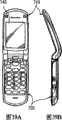
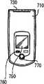
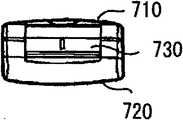
图39A是第五应用例处于打开状态下的正视图;图39B是第五应用例处于打开状态下的侧视图;图39C是第五应用例处于闭合状态下的正视图;图39D是第五应用例处于闭合状态下的左视图;图39E是第五应用例处于闭合状态下的右视图;图39F是第五应用例处于闭合状态下俯视图;以及图39G是第五应用例处于闭合状态下的仰视图。 Fig. 39A is a front view of the fifth application example in an open state; Fig. 39B is a side view of the fifth application example in an open state; Fig. 39C is a front view of the fifth application example in a closed state; Fig. 39D is a fifth application example in a closed state Figure 39E is a right view of the fifth application example in a closed state; Figure 39F is a top view of the fifth application example in a closed state; and Figure 39G is a fifth application example in a closed state bottom view. the
具体实施方式Detailed ways
下面参照附图具体说明本发明的实施例。说明的顺序如下: Embodiments of the present invention will be specifically described below with reference to the accompanying drawings. The order of instructions is as follows:
1.第一实施例(在源极电极和漏极电极中设有开口部的示例); 1. First embodiment (an example in which an opening is provided in a source electrode and a drain electrode);
2.第二实施例(源极电极和漏极电极被槽隔开的示例);以及 2. Second embodiment (example in which source electrode and drain electrode are separated by groove); and
3.第三实施例(在源极电极和漏极电极外部设有突出区域的示例)。 3. Third embodiment (an example in which protruding regions are provided outside the source electrode and the drain electrode). the
1.第一实施例1. The first embodiment
图1图示了本发明第一实施例的显示器件的结构。该显示器件用作超薄型有机发光彩色显示器件等。在该显示器件中,例如,在稍后说明的TFT基板1上形成有显示区域110,在该显示区域110中,由稍后说明的作为显示元件的多个有机发光元件10R、有机发光元件10G和有机发光元件10B构成的像素PXLC以矩阵状态布置着。在显示区域110的周边,形成有作为信号部的水平选择器(HSFL)121以及作为扫描部的写扫描器(WSCN)131和电源扫描器(DSCN)132。 FIG. 1 illustrates the structure of a display device of a first embodiment of the present invention. The display device is used as an ultra-thin organic light-emitting color display device and the like. In this display device, for example, a
在显示区域110中,按照列方向排列有信号线DTL 101~信号线DTL10n,并且按照行方向排列有扫描线WSL 101~扫描线WSL 10m和电源线DSL 101~电源线DSL 10m。在各信号线DTL与各扫描线WSL的交叉部处设置有包含有机发光元件PXLC(10R、10G和10B中的一者(亚像素))的像素电路140。各信号线DTL与水平选择器121连接。从水平选择器121将视频信号提供至信号线DTL。各扫描线WSL与写扫描器131连接。 各电源线DSL与电源扫描仪132连接。 In the
图2图示了像素电路140的示例。像素电路140是包括采样晶体管3A、驱动晶体管3B、保持电容3C和由有机发光元件PXLC构成的发光元件3D的有源驱动电路。采样晶体管3A的栅极与相应的扫描线WSL101连接,采样晶体管3A的源极和漏极中的一者与对应的信号线DTL101连接,并且另一者与驱动晶体管3B的栅极g连接。驱动晶体管3B的漏极d与对应的电源线DSL 101连接,并且驱动晶体管3B的源极s与发光元件3D的阳极连接。发光元件3D的阴极与地线3H连接。地线3H是全部像素PXLC共用的布线。保持电容3C被连接在驱动晶体管3B的源极s与栅极g之间。 FIG. 2 illustrates an example of the
采样晶体管3A根据从扫描线WSL 101供给过来的控制信号而变为导通状态,对从信号线DTL 101供给过来的视频信号的信号电位进行采样,并将结果保持在保持电容3C中。驱动晶体管3B接收从处于第一电位的电源线DSL 101供给过来的电流,并且根据保持电容3C中所保持的信号电位将驱动电流提供至发光元件3D。发光元件3D利用该供给过来的驱动电流以与视频信号的信号电位相对应的亮度进行发光。 The
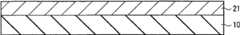
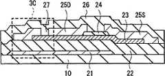
图3图示了用于构成图2所示采样晶体管3A和驱动晶体管3B的TFT 20的平面结构。图4图示了沿图3中的线IV-IV得到的截面结构。TFT 20例如是在基板10上依次形成有栅极电极21、栅极绝缘膜22、氧化物半导体层23、沟道保护层24、源极电极25S、漏极电极25D和钝化膜26的氧化物半导体晶体管。此处的氧化物半导体是指锌、铟、镓或锡等金属的氧化物或者上述金属的混合物的氧化物,并且已知的是,该氧化物半导体呈现出优良的半导体特性。 FIG. 3 illustrates a planar structure of the
栅极电极21通过施加至TFT 20上的栅极电压来控制氧化物半导体层23中的电子密度。栅极电极21例如具有由厚度为50nm的钼(Mo)层和厚度为400nm的铝(Al)层或铝合金层构成的两层结构。铝合金层的示例例如是铝钕合金层。 The
栅极绝缘膜22例如具有约400nm的厚度,并由氧化硅膜、氮化硅膜、氧氮化硅膜或氧化铝膜制成或者由上述膜的层叠膜制成。 The
氧化物半导体层23例如具有20nm以上且100nm以下的厚度,并由铟镓锌氧化物(IGZO)构成。 The
沟道保护层24优选是能使从氧化物半导体薄膜层23脱离的氧量很少并且能向氧化物半导体薄膜层23供给少量氢的层。沟道保护层24例如具有约200nm的厚度,并且由氧化硅膜、氮化硅膜、氧氮化硅膜或氧化铝膜制成或者由上述膜的层叠膜制成。 The channel
源极电极25S和漏极电极25D形成在位于沟道保护层24两侧的氧化物半导体层23上。在氧化物半导体层23中,与源极电极25S与漏极电极25D之间区域对应的部分是沟道区域23A。沟道区域23A被沟道保护层24覆盖着。此外,氧化物半导体层23的沟道宽度方向上的两侧是未被沟道保护层24、源极电极25S及漏极电极25D中的任意一个覆盖的露出部分23B。 The
源极电极25S和漏极电极25D具有使氧化物半导体层23露出的开口部27。因此,在TFT 20中,易于向氧化物半导体层23供氧,并能够恢复优良的晶体管特性。 The
开口部27可设置在源极电极25S和漏极电极25D之一中。此外,开口部27的尺寸、形状和数量不受具体限制。例如,可在一侧的四个位置中布置尺寸为5μm×5μm的开口部27。 The opening
源极电极25S和漏极电极25D例如包括含有铝、铜、银或钼作为主要成分的金属层。源极电极25S和漏极电极25D优选由上述金属层的单层膜制成,或者由层叠膜制成,该层叠膜由上述金属层和含有钛、钒、铌、钽、铬、钨、镍、锌或铟作为主要成分的金属层或金属化合物层构成。 The
特别地,源极电极25S和漏极电极25D优选包括含有铝或铜作为主要成分的金属层,从而能够降低布线的电阻。以铝作为主要成分的金属的示例包括铝、铝钕合金或含有硅的铝。 In particular,
此外,源极电极25S和漏极电极25D的与氧化物半导体层23接触的层优选由不会使氧从氧化物半导体层23中脱离的金属或者不会使氧从氧化物半导体层23中脱离的金属化合物构成,由于使用了这样的金属或 这样的金属化合物,因而TFT 20的电气特性发生变化的可能性很小。具体地,源极电极25S和漏极电极25D的与氧化物半导体层23接触的层优选由下列之一构成:钼;钼的氧化物、氮化物或氧氮化物;钛的氧化物、氮化物或氧氮化物;氮化铝;氧化铜。 In addition, the layers of the
源极电极25S和漏极电极25D的最上层优选由钛构成或者由钛的氧化物、氮化物或氧氮化物构成。 The uppermost layers of the
作为源极电极25S和漏极电极25D的具体结构示例,例如优选从氧化物半导体层23侧层叠有厚度为50nm的钼层25A、厚度为50nm的铝层25B和厚度为50nm的钛层25C的层叠膜,其原因如下所述。在稍后说明的有机发光元件10R、有机发光元件10G和有机发光元件10B的阳极52由含有铝作为主要成分的金属构成的情况下,应当使用含有磷酸、硝酸或醋酸等的混合溶液通过湿式蚀刻方法来设置阳极52。此时,作为最上层的钛层25C具有非常低的蚀刻速率,因而在基板10侧可能留有钛层25C。结果,稍后说明的有机发光元件10R、有机发光元件10G和有机发光元件10B的阴极55可能与基板10侧的钛层25C连接。 As a specific structural example of the
另外,源极电极25S和漏极电极25D的与氧化物半导体层23接触的层优选由金属氧化物或金属氮化物构成。金属氧化物的示例包括氧化钛、氧化铌、氧化锌、氧化锡或铟锡复合氧化物(indium tin compositeoxide,ITO)等。金属氮化物的示例包括氮化钛或氮化钽等。 In addition, the layers of the
钝化膜26例如具有约300nm的厚度,并且由氧化硅膜、氮化硅膜、氧氮化硅膜、氧化铝膜或者它们的层叠膜制成。 The
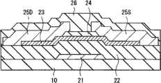
图5图示了显示区域110的截面结构。在显示区域110中,设有产生红光的有机发光元件10R、产生绿光的有机发光元件10G和产生蓝光的有机发光元件10B,这些有机发光元件依次排列着从而在整体上呈矩形状。有机发光元件10R、有机发光元件10G和有机发光元件10B具有片状(reed-like)平面形状,并且彼此相邻的有机发光元件10R、有机发光元件10G和有机发光元件10B的组合构成一个像素。 FIG. 5 illustrates a cross-sectional structure of the
有机发光元件10R、有机发光元件10G和有机发光元件10B分别具有如下结构:在TFT基板1上的平坦化绝缘膜51上,依次层叠有阳极 52、电极间绝缘膜53、包含后述发光层的有机层54以及阴极55。 The organic light-emitting element 10R, the organic light-emitting element 10G, and the organic light-emitting element 10B each have a structure in which an anode 52, an inter-electrode insulating film 53, and an anode including a light-emitting layer described later are stacked in this order on a planarizing insulating film 51 on the
视需要,可将由氮化硅(SiN)或氧化硅(SiO)等构成的保护膜56涂敷到上述有机发光元件10R、有机发光元件10G和有机发光元件10B上。此外,在保护膜56的整个表面上隔着由热固化树脂或紫外线固化树脂等制成的粘接层60与由玻璃等制成的封装基板71粘合,从而密封有机发光元件10R、有机发光元件10G和有机发光元件10B。视需要,在封装基板71上可设有彩色滤光片72和作为黑矩阵的遮光膜(未图示)。 A protective film 56 made of silicon nitride (SiN), silicon oxide (SiO), or the like may be applied to the above-mentioned organic light emitting element 10R, organic light emitting element 10G, and organic light emitting element 10B as needed. In addition, the entire surface of the protective film 56 is bonded to the
平坦化绝缘膜51用于使形成有包括由前述TFT 20构成的采样晶体管3A和驱动晶体管3B的像素电路140的TFT基板1的表面平坦化。由于要在平坦化绝缘膜51中形成微小的连接孔51A,因而平坦化绝缘膜51优选由具有优良的图形精度的材料制成。平坦化绝缘膜51的材料的示例包括诸如聚酰亚胺等有机材料或诸如氧化硅(SiO2)等无机材料。图2所示的驱动晶体管3B通过设在平坦化绝缘膜51中的连接孔51A与阳极52电连接。 The planarizing insulating film 51 is used to planarize the surface of the
阳极52对应于各有机发光元件10R、有机发光元件10G和有机发光元件10B而被形成。此外,阳极52具有反射电极的功能,从而反射在发光层中所产生的光,并且为了提高发光效率,阳极52最好具有尽可能高的反射率。阳极52的厚度例如在100nm以上且1000nm以下。阳极52由诸如银(Ag)、铝(Al)、铬(Cr)、钛(Ti)、铁(Fe)、钴(Co)、镍(Ni)、钼(Mo)、铜(Cu)、钽(Ta)、钨(W)、铂(Pt)或金(Au)等金属元素的单质或合金构成。 The anode 52 is formed corresponding to each of the organic light emitting element 10R, the organic light emitting element 10G, and the organic light emitting element 10B. In addition, the anode 52 functions as a reflective electrode to reflect light generated in the light emitting layer, and in order to improve luminous efficiency, the anode 52 preferably has as high a reflectance as possible. The thickness of the anode 52 is, for example, not less than 100 nm and not more than 1000 nm. The anode 52 is made of such as silver (Ag), aluminum (Al), chromium (Cr), titanium (Ti), iron (Fe), cobalt (Co), nickel (Ni), molybdenum (Mo), copper (Cu), tantalum (Ta), tungsten (W), platinum (Pt) or gold (Au) and other metal elements or alloy composition. the
电极间绝缘膜53用于确保阳极52与阴极55之间的绝缘性,并用于精确地获得发光区域的所需形状。例如,电极间绝缘膜53由诸如聚酰亚胺等有机材料或诸如氧化硅(SiO2)等无机绝缘材料制成。电极间绝缘膜53具有与阳极52的发光区域对应的开口部。有机层54和阴极55可以不仅在发光区域上而且也在电极间绝缘膜53上连续地设置着,此时只有在电极间绝缘膜53的开口部处才会出射光。 The inter-electrode insulating film 53 is used to ensure insulation between the anode 52 and the cathode 55 and to accurately obtain a desired shape of the light emitting region. For example, the interelectrode insulating film 53 is made of an organic material such as polyimide or an inorganic insulating material such as silicon oxide (SiO2 ). The inter-electrode insulating film 53 has an opening corresponding to the light emitting region of the anode 52 . The organic layer 54 and the cathode 55 may be continuously provided not only on the light-emitting region but also on the inter-electrode insulating film 53 . In this case, only the opening of the inter-electrode insulating film 53 emits light.
有机层54例如具有如下结构,即,从阳极52侧依次层叠有空穴注入层、空穴输运层、发光层和电子输运层(未图示)。在上述各层中,除了发光层以外的其他层可以视需要来设置。此外,有机层54的结构可根据 有机发光元件10R、有机发光元件10G和有机发光元件10B的发光颜色的不同而不同。空穴注入层用来提高空穴注入效率,并起到防止泄漏的缓冲层的作用。空穴输运层用于提高向发光层的空穴输运效率。通过施加电场使电子空穴复合,由此让发光层产生光。电子输运层用来增加向发光层的电子输运效率。有机层54的材料不受具体限制,并且可以是普通的低分子有机材料或者普通的高分子有机材料。 The organic layer 54 has, for example, a structure in which a hole injection layer, a hole transport layer, a light emitting layer, and an electron transport layer (not shown) are stacked in this order from the anode 52 side. Among the above-mentioned layers, layers other than the light-emitting layer may be provided as necessary. In addition, the structure of the organic layer 54 may vary depending on the light emission color of the organic light emitting element 10R, the organic light emitting element 10G, and the organic light emitting element 10B. The hole injection layer is used to improve the hole injection efficiency and to function as a buffer layer to prevent leakage. The hole transport layer is used to improve the efficiency of hole transport to the light emitting layer. The light-emitting layer generates light by recombining electrons and holes by applying an electric field. The electron transport layer serves to increase electron transport efficiency to the light emitting layer. The material of the organic layer 54 is not particularly limited, and may be an ordinary low-molecular organic material or an ordinary high-molecular organic material. the
阴极55的厚度例如在5nm以上且50nm以下,并且由诸如铝(Al)、镁(Mg)、钙(Ca)或钠(Na)等金属元素的单质或合金构成。特别地,优选镁和银的合金(MgAg合金)或者铝(Al)和锂(Li)的合金(AlLi合金)。此外,阴极55可由ITO或IZO(铟锌复合氧化物)构成。 The cathode 55 has a thickness of, for example, not less than 5 nm and not more than 50 nm, and is composed of a simple substance or an alloy of a metal element such as aluminum (Al), magnesium (Mg), calcium (Ca), or sodium (Na). In particular, an alloy of magnesium and silver (MgAg alloy) or an alloy of aluminum (Al) and lithium (Li) (AlLi alloy) is preferable. In addition, the cathode 55 may be composed of ITO or IZO (indium zinc composite oxide). the
例如,上述显示器件的制造方法如下。 For example, the manufacturing method of the above-mentioned display device is as follows. the
形成TFT基板1的步骤 Steps of forming
首先,如图6A所示,例如通过溅射方法在由玻璃制成的基板10上形成具有上述厚度且由上述材料制成的金属层。对该金属层进行光刻和蚀刻,从而形成栅极电极21。 First, as shown in FIG. 6A , a metal layer having the above thickness and made of the above material is formed on the
接着,如图6B所示,例如通过等离子体化学气相沉积(ChemicalVapor Deposition,CVD)方法在基板10的整个表面上形成具有上述厚度且由上述材料制成的栅极绝缘膜22。 Next, as shown in FIG. 6B , a
随后,还如图6B所示,通过溅射方法形成具有上述厚度且由上述材料制成的氧化物半导体层23。具体地,在由铟镓锌氧化物(IGZO)构成氧化物半导体层23的情况下,例如通过使用IGZO陶瓷作为靶材的DC(直流)溅射方法,并用氩气(Ar)和氧气(O2)的混合气体进行等离子体放电,由此在基板10上形成IGZO膜。在等离子体放电之前,进行排气直到真空室内部的真空度达到1×10⁻⁴Pa以下,然后导入氩气和氧气的混合气体。在由氧化锌构成氧化物半导体层23的情况下,通过使用氧化锌陶瓷作为靶材的RF(射频)溅射方法,或者通过使用锌金属靶材且在含有氩气和氧气的气体氛围中进行的DC溅射方法,由此形成氧化锌膜。 Subsequently, as also shown in FIG. 6B , the
此后,如图6C所示,通过光刻和蚀刻将氧化物半导体层23成形为预定的形状。随后,再如图6C所示,例如通过等离子体CVD方法形成 具有上述厚度且由上述材料制成的沟道保护层24。通过光刻和蚀刻将沟道保护层24成形为预定的形状。 Thereafter, as shown in FIG. 6C , the
形成沟道保护层24之后,通过例如溅射方法,形成厚度为50nm的钼层25A、厚度为50nm的铝层25B和厚度为50nm的钛层25C。随后,在使用氯基气体通过干式蚀刻法对钛层25C进行蚀刻之后,使用含有磷酸、硝酸和醋酸的混合溶液通过湿式蚀刻法对铝层25B和钼层25A进行蚀刻。因而,如图6D所示,形成了具有开口部27的源极电极25S和漏极电极25D。 After the channel
在形成源极电极25S和漏极电极25D之后,在高温下进行氧退火,因此将氧提供至氧化物半导体层23中缺氧或者脱氧的贫乏部分,从而恢复晶体管特性。作为退火条件,例如可以采用在氮气浓度为60%且氧气浓度为40%的氛围中在300℃下退火1小时。在此情况下,由于在源极电极25S和漏极电极25D中形成有开口部27,并且该开口部27使氧化物半导体层23暴露出来,因此,易于从开口部27向氧化物半导体层23中的贫氧部分供氧。此外,也易于从氧化物半导体层23的露出部分23B向氧化物半导体层23供氧。 After the
此后,通过原子层沉积方法或溅射方法形成具有上述厚度且由上述材料制成的钝化膜26。因此,形成了包含图3和图4所示的TFT 20的TFT基板1。 Thereafter, the
TFT 20的实际制造方法是:由厚度为50nm的钼层25A、厚度为50nm的铝层25B和厚度为50nm的钛层25C构成的层叠膜来形成源极电极25S和漏极电极25D,并且在上述退火条件下对所得到的膜进行退火。对于由此得到的TFT 20,检测其输运特性。结果,如图7A所示,可以得到充分确保了开/关比(on/off ratio)的晶体管特性。 The actual manufacturing method of the
另外,除了使用钛层代替钼层25A以外,按照与上述方式相同的方式制造出另一TFT。对于所得到的TFT,检测其输运特性。结果,如图7B所示,没有得到充分确保了开/关比的晶体管特性。 In addition, another TFT was fabricated in the same manner as above except that a titanium layer was used instead of the
上述结果的原因可能如下。在用由钛、铝和钛构成的三层膜来形成源极电极25S和漏极电极25D的情况下,很难对钛进行湿式蚀刻,因而 通常使用干式蚀刻。为了得到优良的TFT特性,氧化物半导体层23的厚度应为约50nm。然而,在使用干式蚀刻的情况下,很难增大构成源极电极25S和漏极电极25D的金属材料与氧化物半导体之间的选择比。因此,在对源极电极25S和漏极电极25D进行的蚀刻中,除去了氧化物半导体层23。这样,开口部27中没有氧化物半导体层23暴露出来,并且即使在进行氧退火时也很难向氧化物半导体层23供氧。 The reason for the above results may be as follows. In the case where the
形成有机发光元件10R、10G和10B的步骤 Steps of forming organic light-emitting elements 10R, 10G, and 10B
在形成TFT基板1之后,在TFT基板1的整个表面上涂敷感光树脂,并对该感光树脂进行曝光和显影。因此,形成了平坦化绝缘膜51和连接孔51A并进行烘烤。接着,通过例如直流溅射法形成由上述材料制成的阳极52。例如利用光刻技术对所得到的膜进行选择性地蚀刻,从而将其图形化成预定的形状。随后,例如通过CVD方法形成具有上述厚度且由上述材料制成的电极间绝缘膜53,并且例如通过使用光刻技术形成开口部。自那之后,例如通过蒸发沉积方法依次形成由上述材料制成的有机层54和阴极55,从而形成有机发光元件10R、有机发光元件10G和有机发光元件10B。随后,使用由上述材料制成的保护膜56来覆盖有机发光元件10R、有机发光元件10G和有机发光元件10B。 After the
此后,在保护膜56上形成粘接层60。自那之后,准备好设有彩色滤光片72且由上述材料制成的封装基板71。TFT基板1与封装基板71以把粘接层60夹在二者之间的方式相互粘合。因此,完成了图5所示的显示器件。 Thereafter, an adhesive layer 60 is formed on the protective film 56 . After that, the
在该显示器件中,采样晶体管3A根据从扫描线WSL供给过来的控制信号而变为导通,对由信号线DTL供给过来的视频信号的信号电位进行采样,并将该信号电位保持在保持电容3C中。此外,从处于第一电位的电源线DSL将电流提供至驱动晶体管3B,并且根据保持在保持电容3C中的信号电位将驱动电流提供至发光元件3D(有机发光元件10R、有机发光元件10G和有机发光元件10B)。发光元件3D(有机发光元件10R、有机发光元件10G和有机发光元件10B)利用供给过来的驱动电流以与视频信号的信号电位对应的亮度进行发光。该光透过阴极55、彩色滤光片72和封装基板71,然后被获取到。 In this display device, the
在此情况下,在构成采样晶体管3A和驱动晶体管3B的TFT 20中,因为有使氧化物半导体层23露出的开口部27设在源极电极25S和漏极电极25D中,因此,在制造步骤中通过氧退火处理,从开口部27将氧提供至氧化物半导体层23中缺氧或者脱氧的贫乏部分,从而充分地恢复晶体管特性。这样,在利用TFT 20构造而成的显示器件中,抑制了TFT 20的氧化物半导体层23的低阻抗性,抑制了漏电流,并能够以高亮度进行光显示。 In this case, in the
如上所述,在本实施例中,因为在TFT 20的源极电极25S和漏极电极25D中设有使氧化物半导体层23露出的开口部27,因此,易于从开口部27向氧化物半导体层23供氧,并且能够恢复优良的晶体管特性。于是,当使用TFT 20来构造出显示器件时,抑制了TFT 20的氧化物半导体层23的低阻抗性,因此能够抑制漏电流,并且能够以高亮度进行光显示。 As described above, in this embodiment, since the
下面给出本实施例的变形例1-1~变形例1-5的说明。在实际的像素布局中,在某些情况下难以在行间加工(line and space process)中把开口部27设置在源极电极25S或漏极电极25D中。下面的变形例能够解决这种缺点。 A description will be given below of Modification 1-1 to Modification 1-5 of the present embodiment. In an actual pixel layout, it is difficult in some cases to provide the
变形例1-1Modification 1-1
图8图示了变形例1-1的TFT 20的平面结构。图9图示了沿图8中的线IX-IX得到的截面结构。在TFT 20中,漏极电极25D的沟道宽度Wd与源极电极25S的沟道宽度Ws不同,并且使氧化物半导体层23露出的开口部27被设在源极电极25S和漏极电极25D之一的沟道宽度方向的两侧上。因此,在TFT 20中,易于向氧化物半导体层23供氧,并能够恢复优良的晶体管特性。 FIG. 8 illustrates the planar structure of the
具体地,优选源极电极25S的沟道宽度Ws比漏极电极25D的沟道宽度Wd大,并且将开口部27设在漏极电极25D的沟道宽度方向的两侧上。如果将开口部27设在源极电极25S中,则难以充分地确保保持电容3C。 Specifically, it is preferable that the channel width Ws of the
图10图示了使用图8和图9所示TFT 20的像素电路140的平面结 构。TFT 20对采样晶体管3A和驱动晶体管3B都适用,但特别地,优选将该TFT 20应用于驱动晶体管3B,这是因为驱动晶体管3B具有较大的晶体管尺寸。 FIG. 10 illustrates a planar structure of a
变形例1-2Modification 1-2
图11图示了变形例1-2的TFT 20的平面结构。图12图示了沿图11中的线XII-XII得到的截面结构。在TFT 20中,漏极电极25D和源极电极25S之一为喷嘴形状或者梳齿形状。使氧化物半导体层23露出的开口部27设在梳子结构的梳齿之间。因此,在TFT 20中,易于向氧化物半导体层23供氧,并能够恢复优良的晶体管特性。 FIG. 11 illustrates a planar structure of a
具体地,漏极电极25D优选为喷嘴形状或者具有很多梳齿25D1的梳子形状,并且将开口部27设在漏极电极25D的各梳齿25D1之间。如果将开口部27设在源极电极25S中,则难以充分地确保保持电容3C。此外,漏极电极25D的沟道宽度Wd等于各个梳齿25D1的宽度的总和(Wd=Wd1+Wd2+...+Wdn)。源极电极25S的沟道宽度Ws大于漏极电极25D的沟道宽度Wd。 Specifically, the
图13图示了使用图11和图12所示TFT 20的像素电路140的平面结构。TFT 20对采样晶体管3A和驱动晶体管3B都适用,但特别地,优选将该TFT 20应用于驱动晶体管3B,这是因为驱动晶体管3B具有较大的晶体管尺寸。 FIG. 13 illustrates a planar structure of a
变形例1-3Modification 1-3
图14图示了变形例1-3的TFT 20的平面结构。图15图示了沿图14中的线XV-XV得到的截面结构。在TFT 20中,在漏极电极25D中设有沟道宽度减小了的窄沟道宽度区域25D2。使氧化物半导体层23露出的开口部27设在窄沟道宽度区域25D2中。因此,在TFT 20中,易于向氧化物半导体层23供氧,并能够恢复优良的晶体管特性。 FIG. 14 illustrates the planar structure of the
在此情况下,与在源极电极25S的一部分中设置窄沟道宽度区域相比,更优选将窄沟道宽度区域25D2和开口部27设在漏极电极25D的一部分中。如果将开口部27设在源极电极25S中,则难以充分地确保保持电容3C。 In this case, it is more preferable to provide the narrow channel width region 25D2 and the opening
窄沟道宽度区域25D2的平面形状不限于图14所示的矩形,并且可以是如图16所示的诸如梯形等渐锥形状,该渐锥形状是宽度随着窄沟道宽度区域25D2的位置远离源极电极25S而变窄的形状。 The planar shape of the narrow channel width region 25D2 is not limited to the rectangle shown in FIG. 14, and may be a tapered shape such as a trapezoid as shown in FIG. The shape narrows away from the
图17图示了使用图14和图15所示的TFT 20的像素电路140的平面结构。TFT 20对采样晶体管3A和驱动晶体管3B都适用,但特别地,优选将该TFT 20应用于驱动晶体管3B,这是因为驱动晶体管3B具有较大的晶体管尺寸。 FIG. 17 illustrates a planar structure of a
变形例1-4Variation 1-4
图18图示了变形例1-4的像素电路140的平面结构。图19图示了图18所示的驱动晶体管3B的放大平面结构。在像素电路140和驱动晶体管3B中,氧化物半导体层23从漏极电极25D下方的部分延伸至电源线DSL下方的部分。使氧化物半导体层23露出的开口部27设在电源线DSL中。因此,在像素电路140中,易于向驱动晶体管3B的氧化物半导体层23供氧,并能够恢复优良的晶体管特性。 FIG. 18 illustrates a planar structure of a
该变形例对采样晶体管3A和驱动晶体管3B都适用,但特别地,优选将该变形例应用于驱动晶体管3B,这是因为驱动晶体管3B具有较大的晶体管尺寸。此外,由于电源线DSL具有较大的线宽,因而与在扫描线WSL和信号线DTL中设置开口部27相比,开口部27更适合设在电源线DSL中。 This modification is applicable to both the
变形例1-5Variation 1-5
图20图示了变形例1-5的像素电路140的平面结构。图21图示了沿图20中的线XXI-XXI得到的截面结构。在像素电路140和驱动晶体管3B中,氧化物半导体层23从漏极电极25D下方的部分延伸至保持电容3C下方的部分。使氧化物半导体层23露出的开口部27设在保持电容3C中。因此,在像素电路140中,易于向驱动晶体管3B的氧化物半导体层23供氧,并能够恢复优良的晶体管特性。 FIG. 20 illustrates a planar structure of a
2.第二实施例2. The second embodiment
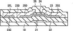
图22图示了第二实施例的TFT 20的平面结构。图23图示了沿图 22中的线XXIII-XXIII得到的截面结构。在图22中,图示了在TFT基板1的像素电路140中构成上述采样晶体管3A的TFT 20和构成上述保持电容3C的电容器30。该TFT 20除了源极电极25S和漏极电极25D在沟道宽度方向上被隔离以外,按照与上述第一实施例相同的方式构造而成。因此,相应的元件用相同的附图标记来进行说明。 FIG. 22 illustrates the planar structure of the
按照与第一实施例相同的方式构造出TFT 20的栅极电极21、栅极绝缘膜22、氧化物半导体层23、沟道保护层24和钝化膜26。 The
源极电极25S和漏极电极25D在沟道宽度方向上被槽28隔开。在槽28中,氧化物半导体层23被暴露出来。因此,在TFT 20中,易于向氧化物半导体层23供氧,并能够恢复优良的晶体管特性。 The
沟道区域23A最好形成在与槽28相距20μm以内的区域中。氧的输运是在穿过氧化物半导体层23内或者穿过氧化物半导体层23与其他层之间界面的水平方向上进行的输运。因而,当在与槽28相距20μm以内的区域中形成沟道区域23A时,能够进一步提高槽28的效果。
表1图示了通过检测沟道宽度W(在与源极电极25S和漏极电极25D的相互面对方向垂直的方向上的宽度,即,在源极电极25S和漏极电极25D的纵长方向上的宽度)和沟道长度L(在源极电极25S和漏极电极25D相互面对的方向上的宽度)与晶体管特性之间的关系而得到的结果。从表1明显可知,在图24所示的W为20μm且L为10μm的情况下,显示出了优良的晶体管特性。同时,在图25所示的W为50μm且L为10μm的情况下,耗尽型操作转变成导电体操作。作为参考,在图26中,图示了表1中W为20μm且L为20μm的情况下的晶体管特性(良好)和W为50μm且L为20μm的情况下的晶体管特性(导电体操作)。 Table 1 illustrates by detecting the channel width W (the width in the direction perpendicular to the mutual facing direction of the
表1 Table 1
(单位:μm) (unit: μm)
在如图24和图25所示的TFT 20中,仅从在氧化物半导体层23的沟道宽度方向的两端上的露出部分23B供氧。因此,氧输运距离变成W/2。在图24中,氧输运距离为W/2=10μm,并且得到了良好的晶体管特性。同时,在图25中,氧输运距离为W/2=25μm,并且状态转变成导电体操作。因此,可以认为,在形成了槽28的情况下,如果氧输运距离为10μm以下,也就是说,如果在与槽28相距20μm以内的区域中形成沟道区域23A,则能够从槽28和露出部分23B向氧化物半导体层23充分地供氧。 In the
电容器30包括从基板10侧依次形成的与栅极电极21形成在同一层的下层电极、与栅极绝缘膜22形成在同一层的电容绝缘膜以及与源极电极25S和漏极电极25D形成在同一层的上层电极。 The
可按照与第一实施例相同的方式来制造出TFT 20和包括TFT 20的显示器件。 The
在该显示器件中,与第一实施例相同,发光元件3D(有机发光元件10R、有机发光元件10G和有机发光元件10B)发光,并且该光透过阴极55、彩色滤光片72和封装基板71然后被获取到。在此情况下,在构成采样晶体管3A和驱动晶体管3B的TFT 20中,源极电极25S和漏极电极25D在沟道宽度方向上被使氧化物半导体层23露出的槽28隔开。因此,在制造步骤中通过氧退火处理,从开口部27向氧化物半导体层23中缺氧或者脱氧的贫乏部分供氧,并充分地恢复晶体管特性。因此,在使用TFT 20构造而成的显示器件中,能够抑制TFT 20的氧化物半导体层23的低阻抗性,抑制漏电流,并能够以高亮度进行光显示。 In this display device, as in the first embodiment, the light-emitting
如上所述,在本实施例中,源极电极25S和漏极电极25D在沟道宽度方向上被使氧化物半导体层23暴露出来的槽28隔开。因而,易于从槽28向氧化物半导体层23供氧,并能够恢复优良的晶体管特性。因此,如果使用TFT 20来构造出显示器件,则抑制了TFT 20的氧化物半导体层23的低阻抗性,因而能够抑制漏电流,并且能够以高亮度进行光显示。 As described above, in the present embodiment, the
3.第三实施例3. The third embodiment
图27图示了本发明第三实施例的TFT 20的平面结构。该TFT 20 除了氧化物半导体层23在漏极电极25D的一侧露出以外,按照与上述第一实施例和第二实施例相同的方式构造而成。因此,相应的元件用相同的附图标记来进行说明。 FIG. 27 illustrates a planar structure of a
按照与第一实施例相同的方式构造出TFT 20的栅极电极21、栅极绝缘膜22、氧化物半导体层23、沟道保护层24和钝化膜26。 The
沿着漏极电极25D的与沟道保护层24重叠的一侧的相对侧设有氧化物半导体层23从漏极电极25D的端部露出的突出区域29。因而,在TFT 20中,易于向氧化物半导体层23供氧,并能够恢复优良的晶体管特性。 A protruding
与第二实施例相同,优选将沟道区域23A形成在与突出区域29相距20μm以内的区域中。 As in the second embodiment, it is preferable to form the
可按照与第一实施例相同的方式制造出TFT 20和包括TFT 20的显示器件。 The
在本显示器件中,与第一实施例相同,发光元件3D(有机发光元件10R、有机发光元件10G和有机发光元件10B)发光,该光透过阴极55、彩色滤光片72和封装基板71然后被获取到。在此情况下,在构成采样晶体管3A和驱动晶体管3B的TFT 20中,沿着漏极电极25D的与沟道保护层24重叠的一侧的相对侧设有氧化物半导体层23从漏极电极25D的端部露出的突出区域29。因而,在制造步骤中通过氧退火处理,向氧化物半导体层23中缺氧或者脱氧的贫乏部分供氧,并充分地恢复晶体管特性。因此,在使用TFT 20构造而成的显示器件中,抑制了TFT 20的氧化物半导体层23的低阻抗性,抑制了漏电流,并且能够以高亮度进行光显示。 In this display device, as in the first embodiment, the
如上所述,在本实施例中,沿着漏极电极25D的与沟道保护层24重叠的一侧的相对侧设有氧化物半导体层23从漏极电极25D的端部露出的突出区域29。因而,易于从突出区域29向氧化物半导体层23供氧,并能够恢复优良的晶体管特性。因此,在使用TFT 20构造出显示器件的情况下,抑制了TFT 20的氧化物半导体层23的低阻抗性,从而能够抑制漏电流,并且能够以高亮度进行光显示。 As described above, in the present embodiment, the protruding
变形例3-1Variation 3-1
在上述实施例中,已经对突出区域29设置在漏极电极25D的一侧上的情况进行了说明。然而,如图28和图29所示,根据TFT 20的结构,也可将突出区域29设置在源极电极25S和漏极电极25D的外侧。 In the above-described embodiments, the case where the projected
变形例3-2Variation 3-2
图30图示了变形例3-2的像素电路140的平面结构。图31图示了图30所示的采样晶体管3A和信号线DTL的截面结构。在像素电路140中,氧化物半导体层23从源极电极25S或漏极电极25D下方的部分延伸至诸如信号线DTL和电源线DSL等布线下方的部分。突出区域29设置在诸如信号线DTL和电源线DSL等布线中。因此,在像素电路140中,易于向采样晶体管3A或驱动晶体管3B的氧化物半导体层23供氧,并能够恢复优良的晶体管特性。 FIG. 30 illustrates a planar structure of a
变形例3-3Variation 3-3
图32图示了变形例3-3的像素电路140的平面结构。图33图示了图32所示的采样晶体管3A和信号线DTL的截面结构。在像素电路140中,在诸如扫描线WSL、信号线DTL和电源线DSL等布线的下方设有下层布线氧化物半导体层23C。该下层布线氧化物半导体层23C通过隔离槽23D与作为采样晶体管3A或驱动晶体管3B的活性层的氧化物半导体层23隔开。诸如扫描线WSL、信号线DTL和电源线DSL等布线的宽度大于下层布线氧化物半导体层23C的宽度,并且这些布线覆盖下层布线氧化物半导体层23C的整个表面。因此,在下层布线氧化物半导体层23C中,在制造步骤中氧始终被脱离,并且没有通过退火处理引入用于恢复氧化物半导体层23的特性的氧。下层布线氧化物半导体层23C具有金属的特性,并且构成布线的一部分。此外,能够使用与氧化物半导体层23的掩模相同的掩模来形成下层布线氧化物半导体层23C。因而,在像素电路140中,不必使用多个掩模,也能够降低扫描线WSL、信号线DTL或电源线DSL的电阻。因此,能够以低成本抑制布线电阻所引起的诸如串扰或阴影等图像失真。 FIG. 32 illustrates a planar structure of a
模块和应用例Modules and Application Examples
下面说明在上述各实施例中说明的显示器件的应用例。上述各实施例的显示器件适合于用于把从外部输入的视频信号或者在内部产生的视频信号以图像或视频的方式进行显示的任何领域中的电子装置的显示器件,上述电子装置例如是电视机、数码相机、笔记本电脑、诸如手机等便携式终端装置、摄像机等。 Application examples of the display devices described in the above embodiments will be described below. The display devices of the above-mentioned embodiments are suitable for display devices of electronic devices in any field that display video signals input from the outside or internally generated video signals in the form of images or videos. The above-mentioned electronic devices are, for example, televisions PCs, digital cameras, notebook computers, portable terminal devices such as mobile phones, video cameras, etc. the
模块 module
将上述各实施例的显示器件作为例如图34所示的模块而装配至诸如后述的第一应用例~第五应用例的各种电子装置中。在该模块中,例如,在基板11的一边设有从封装基板71和粘接层60露出的区域210,并且在该露出的区域210中通过延长信号线驱动电路120的布线和扫描线驱动电路130的布线而形成外部连接端子(未图示)。这些外部连接端子可以设有用于输入及输出信号的柔性印刷电路(Flexible Printed Circuit,FPC)220。 The display devices of the above-described embodiments are incorporated into various electronic devices such as the first to fifth application examples described later as modules shown in FIG. 34 , for example. In this module, for example, an
第一应用例 The first application example
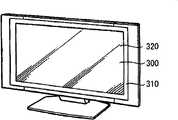
图35图示了应用上述实施例的显示器件的电视机的外观。该电视机例如具有包括前面板310和滤光玻璃320的视频显示屏部300。该视频显示屏部300由任一上述实施例的显示器件构成。 FIG. 35 illustrates the appearance of a television set to which the display device of the above-described embodiment is applied. This television has, for example, a
第二应用例 The second application example
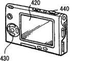
图36A和图36B图示了应用上述实施例的显示器件的数码相机的外观。该数码相机例如包括闪光用的发光部410、显示部420、菜单开关430和快门按钮440。该显示部420由任一上述实施例的显示器件构成。 36A and 36B illustrate the appearance of a digital camera to which the display device of the above-described embodiment is applied. This digital camera includes, for example, a
第三应用例 The third application example
图37图示了应用上述实施例的显示器件的笔记本电脑的外观。该笔记本电脑例如包括主体510、用于进行字符等的输入操作的键盘520和用于显示图像的显示部530。该显示部530由任一上述实施例的显示器件构成。 FIG. 37 illustrates the appearance of a notebook computer to which the display device of the above-described embodiment is applied. This notebook computer includes, for example, a
第四应用例 The fourth application example
图38图示了应用上述实施例的显示器件的摄像机的外观。该摄像机例如包括主体610、设在主体610的前侧面上且用于拍摄物体的镜头620、拍摄开始/停止开关630和显示部640。该显示部640由任一上述实施例的显示器件构成。 FIG. 38 illustrates the appearance of a video camera to which the display device of the above-described embodiment is applied. The video camera includes, for example, a main body 610 , a lens 620 provided on the front side of the main body 610 for photographing a subject, a photographing start/stop switch 630 , and a display portion 640 . The display unit 640 is constituted by any of the display devices of the above-mentioned embodiments. the
第五应用例 The fifth application example
图39A~图39G图示了应用上述实施例的显示器件的手机的外观。在该手机中,例如上壳体710和下壳体720通过连接部(铰链部)730连接在一起。该手机包括显示部740、副显示部750、图片灯760和照相机770。该显示部740或该副显示部750由任一上述实施例的显示器件构成。 39A to 39G illustrate the appearance of a mobile phone to which the display device of the above-described embodiment is applied. In this mobile phone, for example, an
虽然参照各实施例说明了本发明,但本发明不限于上述各实施例,可以作出各种修改。例如,各层的材料、厚度、成膜方法、成膜条件等不限于上述各实施例中所述的那些,也可以采用其他材料、其他厚度、其他成膜方法和其他成膜条件。 Although the present invention has been described with reference to the respective embodiments, the present invention is not limited to the above-described respective embodiments, and various modifications can be made. For example, the materials, thicknesses, film-forming methods, and film-forming conditions of each layer are not limited to those described in the above embodiments, and other materials, other thicknesses, other film-forming methods, and other film-forming conditions can also be used. the
此外,在上述各实施例中,说明了有机发光元件10R、有机发光元件10B和有机发光元件10G具有在TFT基板1上依次层叠有阳极52、包含发光层的有机层54和阴极55的结构的情况。然而,层叠顺序不限于上述,只要有机发光元件10R、有机发光元件10B和有机发光元件10G具有位于阳极52与阴极55之间且包含发光层的有机层54即可。例如,有机发光元件10R、有机发光元件10B和有机发光元件10G可具有在TFT基板1上依次层叠有阴极55、包含发光层的有机层54和阳极52的结构。 In addition, in each of the above-mentioned embodiments, it was described that the organic light emitting element 10R, the organic light emitting element 10B, and the organic light emitting element 10G have a structure in which the anode 52 , the organic layer 54 including the light emitting layer, and the cathode 55 are sequentially stacked on the
此外,在上述各实施例中,用具体示例说明了有机发光元件10R、有机发光元件10B和有机发光元件10G。然而,上述所有层并不是都必需设置的,并且还可以设置有其他层。 Furthermore, in each of the above-described embodiments, the organic light emitting element 10R, the organic light emitting element 10B, and the organic light emitting element 10G have been described with specific examples. However, not all of the above-mentioned layers are necessarily provided, and other layers may also be provided. the
另外,本发明除了适用于包含有机发光元件的显示器件之外,还适用于包含诸如液晶显示元件、无机电致发光元件、电沉积显示元件(electrodeposition display device)或电铬显示元件(electrochromic display device)等其他显示元件的显示器件。 In addition, in addition to being applicable to display devices including organic light-emitting elements, the present invention is also applicable to display devices including liquid crystal display elements, inorganic electroluminescence elements, electrodeposition display devices (electrodeposition display device) or electrochromic display devices (electrochromic display device) ) and other display devices such as display elements. the
本领域技术人员应当理解,依据设计要求和其他因素,可以在本发明所附的权利要求或其等同物的范围内进行各种修改、组合、次组合及改变。 It should be understood by those skilled in the art that various modifications, combinations, sub-combinations and changes can be made within the scope of the appended claims of the present invention or their equivalents according to design requirements and other factors. the
Claims (15)
Translated fromChineseApplications Claiming Priority (2)
| Application Number | Priority Date | Filing Date | Title |
|---|---|---|---|
| JP2009027646AJP4752927B2 (en) | 2009-02-09 | 2009-02-09 | Thin film transistor and display device |
| JP2009-027646 | 2009-02-09 |
Publications (2)
| Publication Number | Publication Date |
|---|---|
| CN101800248A CN101800248A (en) | 2010-08-11 |
| CN101800248Btrue CN101800248B (en) | 2012-06-20 |
Family
ID=42539679
Family Applications (1)
| Application Number | Title | Priority Date | Filing Date |
|---|---|---|---|
| CN201010104366.5AActiveCN101800248B (en) | 2009-02-09 | 2010-02-02 | Thin film transistor and display unit |
Country Status (5)
| Country | Link |
|---|---|
| US (2) | US8269217B2 (en) |
| JP (1) | JP4752927B2 (en) |
| KR (1) | KR101651679B1 (en) |
| CN (1) | CN101800248B (en) |
| TW (1) | TWI412137B (en) |
Families Citing this family (79)
| Publication number | Priority date | Publication date | Assignee | Title |
|---|---|---|---|---|
| KR101041144B1 (en)* | 2009-08-13 | 2011-06-13 | 삼성모바일디스플레이주식회사 | Thin film transistor, manufacturing method thereof and organic light emitting display device comprising same |
| JP5458102B2 (en)* | 2009-09-04 | 2014-04-02 | 株式会社東芝 | Thin film transistor manufacturing method |
| CN102511082B (en)* | 2009-09-16 | 2016-04-27 | 株式会社半导体能源研究所 | Semiconductor device and manufacturing method thereof |
| KR20220127372A (en) | 2009-09-24 | 2022-09-19 | 가부시키가이샤 한도오따이 에네루기 켄큐쇼 | Oxide semiconductor film and semiconductor device |
| KR101843558B1 (en)* | 2009-10-09 | 2018-03-30 | 가부시키가이샤 한도오따이 에네루기 켄큐쇼 | Shift register and display device and driving method thereof |
| CN105702688B (en) | 2009-10-21 | 2020-09-08 | 株式会社半导体能源研究所 | Liquid crystal display device and electronic apparatus including the same |
| WO2011065243A1 (en) | 2009-11-28 | 2011-06-03 | Semiconductor Energy Laboratory Co., Ltd. | Semiconductor device and manufacturing method thereof |
| US8780629B2 (en)* | 2010-01-15 | 2014-07-15 | Semiconductor Energy Laboratory Co., Ltd. | Semiconductor device and driving method thereof |
| KR20190093706A (en) | 2010-01-24 | 2019-08-09 | 가부시키가이샤 한도오따이 에네루기 켄큐쇼 | Display device and manufacturing method thereof |
| CN102822980B (en) | 2010-03-26 | 2015-12-16 | 株式会社半导体能源研究所 | Manufacturing method of semiconductor device |
| US9147768B2 (en)* | 2010-04-02 | 2015-09-29 | Semiconductor Energy Laboratory Co., Ltd. | Semiconductor device having an oxide semiconductor and a metal oxide film |
| KR102276768B1 (en) | 2010-04-02 | 2021-07-13 | 가부시키가이샤 한도오따이 에네루기 켄큐쇼 | Semiconductor device |
| KR102436902B1 (en) | 2010-04-02 | 2022-08-25 | 가부시키가이샤 한도오따이 에네루기 켄큐쇼 | Semiconductor device |
| US9196739B2 (en)* | 2010-04-02 | 2015-11-24 | Semiconductor Energy Laboratory Co., Ltd. | Semiconductor device including oxide semiconductor film and metal oxide film |
| US8884282B2 (en) | 2010-04-02 | 2014-11-11 | Semiconductor Energy Laboratory Co., Ltd. | Semiconductor device |
| US9190522B2 (en) | 2010-04-02 | 2015-11-17 | Semiconductor Energy Laboratory Co., Ltd. | Semiconductor device having an oxide semiconductor |
| US8653514B2 (en) | 2010-04-09 | 2014-02-18 | Semiconductor Energy Laboratory Co., Ltd. | Semiconductor device and method for manufacturing the same |
| WO2011162177A1 (en)* | 2010-06-21 | 2011-12-29 | 株式会社アルバック | Semiconductor device, liquid crystal display device including semiconductor device, and process for producing semiconductor device |
| US9246010B2 (en)* | 2010-07-14 | 2016-01-26 | Sharp Kabushiki Kaisha | Thin film transistor substrate |
| EP2426720A1 (en)* | 2010-09-03 | 2012-03-07 | Applied Materials, Inc. | Staggered thin film transistor and method of forming the same |
| WO2012029596A1 (en)* | 2010-09-03 | 2012-03-08 | Semiconductor Energy Laboratory Co., Ltd. | Method for manufacturing semiconductor device |
| KR101989392B1 (en)* | 2010-10-20 | 2019-06-14 | 가부시키가이샤 한도오따이 에네루기 켄큐쇼 | Method for driving semiconductor deivce |
| CN102097324B (en)* | 2010-10-22 | 2012-12-12 | 友达光电股份有限公司 | Semiconductor element and its manufacturing method |
| KR20120045178A (en)* | 2010-10-29 | 2012-05-09 | 삼성전자주식회사 | Thin film transistor and method of manufacturing the same |
| TWI572009B (en) | 2011-01-14 | 2017-02-21 | 半導體能源研究所股份有限公司 | Semiconductor memory device |
| CN102610652A (en)* | 2011-01-20 | 2012-07-25 | 元太科技工业股份有限公司 | Metal oxide semiconductor structure and manufacturing method thereof |
| TWI624878B (en) | 2011-03-11 | 2018-05-21 | 半導體能源研究所股份有限公司 | Semiconductor device manufacturing method |
| WO2012153473A1 (en)* | 2011-05-06 | 2012-11-15 | Semiconductor Energy Laboratory Co., Ltd. | Semiconductor device |
| JP4982619B1 (en) | 2011-07-29 | 2012-07-25 | 富士フイルム株式会社 | Manufacturing method of semiconductor element and manufacturing method of field effect transistor |
| KR101506303B1 (en)* | 2011-09-29 | 2015-03-26 | 가부시키가이샤 한도오따이 에네루기 켄큐쇼 | Semiconductor device and method for manufacturing the same |
| CN103229301B (en)* | 2011-11-29 | 2017-02-08 | 株式会社日本有机雷特显示器 | Thin film transistor and manufacture method thereof |
| TWI463670B (en) | 2012-03-28 | 2014-12-01 | E Ink Holdings Inc | Active component |
| CN104205341B (en)* | 2012-04-04 | 2017-04-05 | 夏普株式会社 | Semiconductor device and its manufacture method |
| KR101949225B1 (en) | 2012-04-16 | 2019-04-26 | 삼성디스플레이 주식회사 | Thin film transistor and display device having the same |
| JP6001308B2 (en)* | 2012-04-17 | 2016-10-05 | 株式会社半導体エネルギー研究所 | Semiconductor device |
| US9048323B2 (en) | 2012-04-30 | 2015-06-02 | Semiconductor Energy Laboratory Co., Ltd. | Semiconductor device |
| JP5991668B2 (en)* | 2012-08-23 | 2016-09-14 | 株式会社ジャパンディスプレイ | Display device and manufacturing method thereof |
| US9331165B2 (en) | 2012-11-02 | 2016-05-03 | Boe Technology Group Co., Ltd. | Thin-film transistor (TFT), manufacturing method thereof, array substrate, display device and barrier layer |
| JP6285150B2 (en)* | 2012-11-16 | 2018-02-28 | 株式会社半導体エネルギー研究所 | Semiconductor device |
| TWI624949B (en) | 2012-11-30 | 2018-05-21 | 半導體能源研究所股份有限公司 | Semiconductor device |
| CN103050441B (en)* | 2012-12-10 | 2014-09-24 | 华映视讯(吴江)有限公司 | Oxide thin film transistor preparation method |
| TWI597849B (en)* | 2012-12-28 | 2017-09-01 | 神戶製鋼所股份有限公司 | Thin film transistor and method of manufacturing the same |
| CN103177970A (en)* | 2013-02-26 | 2013-06-26 | 上海大学 | Method for manufacturing oxide thin-film transistor |
| JP6151070B2 (en)* | 2013-04-11 | 2017-06-21 | 株式会社ジャパンディスプレイ | THIN FILM TRANSISTOR AND DISPLAY DEVICE USING THE SAME |
| TWI513005B (en)* | 2013-09-13 | 2015-12-11 | Au Optronics Corp | Thin film transistor and method of manufacturing same |
| TWI677989B (en) | 2013-09-19 | 2019-11-21 | 日商半導體能源研究所股份有限公司 | Semiconductor device and manufacturing method thereof |
| KR102085099B1 (en)* | 2013-10-15 | 2020-03-05 | 삼성디스플레이 주식회사 | Thin film transistor substrates, display devices and methods of manufacturing display devices |
| KR102232539B1 (en)* | 2013-11-13 | 2021-03-29 | 삼성디스플레이 주식회사 | Thin film transistor, display substrate having the same and method of manufacturing a thin film transistor |
| JP6227016B2 (en)* | 2014-02-14 | 2017-11-08 | シャープ株式会社 | Active matrix substrate |
| US9166181B2 (en) | 2014-02-19 | 2015-10-20 | International Business Machines Corporation | Hybrid junction field-effect transistor and active matrix structure |
| JP2015158572A (en)* | 2014-02-24 | 2015-09-03 | 株式会社Joled | Display device, electronic apparatus |
| US20150340539A1 (en)* | 2014-05-21 | 2015-11-26 | Semiconductor Energy Laboratory Co., Ltd. | Ultraviolet sensor and electronic device using ultraviolet sensor |
| CN104167446B (en)* | 2014-07-14 | 2017-09-29 | 京东方科技集团股份有限公司 | A kind of thin film transistor (TFT), array base palte and display device |
| WO2016035652A1 (en)* | 2014-09-03 | 2016-03-10 | シャープ株式会社 | Method for manufacturing metal lamination film, method for manufacturing semiconductor device, and method for manufacturing liquid crystal display device |
| CN104600123B (en)* | 2015-01-05 | 2018-06-26 | 京东方科技集团股份有限公司 | A kind of thin film transistor (TFT) and preparation method thereof, array substrate and display device |
| KR102441560B1 (en) | 2015-04-07 | 2022-09-08 | 삼성디스플레이 주식회사 | Thin film transistor array substrate and organic light emitting display device having same |
| CN104934330A (en)* | 2015-05-08 | 2015-09-23 | 京东方科技集团股份有限公司 | Film transistor and preparation method thereof, array substrate and display panel |
| CN106684125B (en)* | 2015-11-05 | 2020-05-08 | 群创光电股份有限公司 | display screen |
| US20180356660A1 (en)* | 2015-12-09 | 2018-12-13 | Sharp Kabushiki Kaisha | Active matrix substrate and liquid crystal display panel provided with same |
| CN106887436B (en)* | 2015-12-16 | 2019-10-25 | 鸿富锦精密工业(深圳)有限公司 | Thin film transistor array substrate and preparation method thereof |
| JP2017143108A (en)* | 2016-02-08 | 2017-08-17 | 株式会社ジャパンディスプレイ | Thin film transistor and method of manufacturing thin film transistor |
| TWI715699B (en)* | 2016-10-21 | 2021-01-11 | 日商半導體能源硏究所股份有限公司 | Composite oxide and transistor |
| CN106653772B (en)* | 2016-12-30 | 2019-10-01 | 惠科股份有限公司 | A display panel and its manufacturing process |
| KR20180099974A (en) | 2017-02-27 | 2018-09-06 | 삼성디스플레이 주식회사 | Semiconductor device and method for fabricating the same |
| US10510899B2 (en) | 2017-08-07 | 2019-12-17 | Wuhan China Star Optoelectronics Semiconductor Display Technology Co., Ltd. | Thin film transistor, thin film transistor manufacturing method and liquid crystal display panel |
| CN107369718A (en)* | 2017-08-07 | 2017-11-21 | 武汉华星光电半导体显示技术有限公司 | Thin film transistor (TFT) and its manufacture method, liquid crystal display panel |
| KR20190047365A (en)* | 2017-10-27 | 2019-05-08 | 경희대학교 산학협력단 | Oxide semiconductor thin film transistor and method of manufacturing the same |
| JP2019153656A (en)* | 2018-03-02 | 2019-09-12 | シャープ株式会社 | Active matrix substrate and demultiplexer circuit |
| CN109616510B (en)* | 2018-12-03 | 2020-04-14 | 惠科股份有限公司 | Thin film transistor structure and method of making the same, and display device |
| JP7327940B2 (en)* | 2019-01-10 | 2023-08-16 | 株式会社ジャパンディスプレイ | Semiconductor device and display device |
| US10784341B2 (en)* | 2019-01-21 | 2020-09-22 | Northrop Grumnian Systems Corporation | Castellated superjunction transistors |
| CN110707156B (en)* | 2019-09-16 | 2023-11-28 | Tcl华星光电技术有限公司 | Thin film transistor and manufacturing method thereof |
| CN111244034A (en)* | 2020-01-17 | 2020-06-05 | Tcl华星光电技术有限公司 | Array substrate and manufacturing method thereof |
| CN111403336A (en)* | 2020-03-31 | 2020-07-10 | 成都中电熊猫显示科技有限公司 | Array substrate, display panel and manufacturing method of array substrate |
| US11631704B2 (en)* | 2020-04-21 | 2023-04-18 | Sharp Kabushiki Kaisha | Active matrix substrate and display device |
| CN111682033A (en)* | 2020-07-07 | 2020-09-18 | 深圳市华星光电半导体显示技术有限公司 | Display panel and method of making the same |
| CN114883345B (en)* | 2022-05-06 | 2025-09-12 | 深圳市华星光电半导体显示技术有限公司 | Driving backplane and manufacturing method thereof, and display panel |
| WO2023239182A1 (en)* | 2022-06-09 | 2023-12-14 | 서울대학교산학협력단 | Thin film transistor driving device and method for manufacturing same |
| CN115101537A (en)* | 2022-06-22 | 2022-09-23 | 合肥维信诺科技有限公司 | Array substrate and display panel |
Citations (3)
| Publication number | Priority date | Publication date | Assignee | Title |
|---|---|---|---|---|
| CN1918672A (en)* | 2004-03-09 | 2007-02-21 | 出光兴产株式会社 | Thin film transistor, thin film transistor substrate, method for producing thin film transistor substrate, liquid crystal display device using thin film transistor substrate, apparatus and method for producing thin film transistor substrate, sputtering target, transparent conductive film and transparent electrode formed by using sputtering target, and apparatus and method for producing thin film transistor substrate |
| US7265384B2 (en)* | 2004-04-28 | 2007-09-04 | Samsung Sdi Co., Ltd. | Thin film transistor and organic electroluminescence display using the same |
| CN101335293A (en)* | 2005-09-29 | 2008-12-31 | 株式会社半导体能源研究所 | Semiconductor device and manufacturing method thereof |
Family Cites Families (29)
| Publication number | Priority date | Publication date | Assignee | Title |
|---|---|---|---|---|
| JPH0261620A (en)* | 1988-08-29 | 1990-03-01 | Hitachi Ltd | liquid crystal display device |
| JP3856901B2 (en)* | 1997-04-15 | 2006-12-13 | 株式会社半導体エネルギー研究所 | Display device |
| JP2915397B1 (en)* | 1998-05-01 | 1999-07-05 | インターナショナル・ビジネス・マシーンズ・コーポレイション | Thin film transistor for preventing back channel effect and method of manufacturing the same |
| US6346730B1 (en)* | 1999-04-06 | 2002-02-12 | Semiconductor Energy Laboratory Co., Ltd. | Liquid crystal display device having a pixel TFT formed in a display region and a drive circuit formed in the periphery of the display region on the same substrate |
| JP4403599B2 (en)* | 1999-04-19 | 2010-01-27 | ソニー株式会社 | Semiconductor thin film crystallization method, laser irradiation apparatus, thin film transistor manufacturing method, and display apparatus manufacturing method |
| JP2001119029A (en)* | 1999-10-18 | 2001-04-27 | Fujitsu Ltd | Thin film transistor, method of manufacturing the same, and liquid crystal display device having the same |
| JP2001209070A (en)* | 2000-01-27 | 2001-08-03 | Casio Comput Co Ltd | Liquid crystal display device |
| US6559594B2 (en)* | 2000-02-03 | 2003-05-06 | Semiconductor Energy Laboratory Co., Ltd. | Light-emitting device |
| JP2001284592A (en)* | 2000-03-29 | 2001-10-12 | Sony Corp | Thin film semiconductor device and driving method thereof |
| US6774397B2 (en)* | 2000-05-12 | 2004-08-10 | Semiconductor Energy Laboratory Co., Ltd. | Semiconductor device |
| SG138468A1 (en)* | 2001-02-28 | 2008-01-28 | Semiconductor Energy Lab | A method of manufacturing a semiconductor device |
| JP4024508B2 (en)* | 2001-10-09 | 2007-12-19 | 株式会社半導体エネルギー研究所 | Method for manufacturing semiconductor device |
| US6833556B2 (en)* | 2002-08-12 | 2004-12-21 | Acorn Technologies, Inc. | Insulated gate field effect transistor having passivated schottky barriers to the channel |
| US7868957B2 (en)* | 2003-12-02 | 2011-01-11 | Semiconductor Energy Laboratory Co., Ltd. | Thin film transistor, display device and liquid crystal display device and method for manufacturing the same |
| JP4245158B2 (en)* | 2004-04-19 | 2009-03-25 | パナソニック株式会社 | FET type ferroelectric memory cell and FET type ferroelectric memory |
| US20050258427A1 (en)* | 2004-05-20 | 2005-11-24 | Chan Isaac W T | Vertical thin film transistor electronics |
| JP2006126692A (en)* | 2004-11-01 | 2006-05-18 | Seiko Epson Corp | Thin film pattern substrate, device manufacturing method, electro-optical device, and electronic apparatus |
| JP5053537B2 (en) | 2004-11-10 | 2012-10-17 | キヤノン株式会社 | Semiconductor device using amorphous oxide |
| JP5138163B2 (en) | 2004-11-10 | 2013-02-06 | キヤノン株式会社 | Field effect transistor |
| US20080210934A1 (en)* | 2005-03-25 | 2008-09-04 | Tokyo Institute Of Technology | Semiconductor Device Using Titanium Dioxide as Active Layer and Method for Producing Semiconductor Device |
| JP5064747B2 (en)* | 2005-09-29 | 2012-10-31 | 株式会社半導体エネルギー研究所 | Semiconductor device, electrophoretic display device, display module, electronic device, and method for manufacturing semiconductor device |
| JP2007115808A (en) | 2005-10-19 | 2007-05-10 | Toppan Printing Co Ltd | Transistor |
| JP2007212699A (en)* | 2006-02-09 | 2007-08-23 | Idemitsu Kosan Co Ltd | Reflective TFT substrate and manufacturing method of reflective TFT substrate |
| KR101035737B1 (en)* | 2006-03-15 | 2011-05-20 | 샤프 가부시키가이샤 | Active Matrix Substrate, Display Device and Television Receiver |
| US20080023703A1 (en)* | 2006-07-31 | 2008-01-31 | Randy Hoffman | System and method for manufacturing a thin-film device |
| JP5121254B2 (en)* | 2007-02-28 | 2013-01-16 | キヤノン株式会社 | Thin film transistor and display device |
| KR100851215B1 (en)* | 2007-03-14 | 2008-08-07 | 삼성에스디아이 주식회사 | Thin film transistor and organic light emitting display device using same |
| US20090278120A1 (en)* | 2008-05-09 | 2009-11-12 | Korea Institute Of Science And Technology | Thin Film Transistor |
| TWI424506B (en)* | 2008-08-08 | 2014-01-21 | Semiconductor Energy Lab | Semiconductor device manufacturing method |
- 2009
- 2009-02-09JPJP2009027646Apatent/JP4752927B2/enactiveActive
- 2010
- 2010-01-27TWTW099102266Apatent/TWI412137B/enactive
- 2010-01-29USUS12/696,270patent/US8269217B2/enactiveActive
- 2010-02-01KRKR1020100008969Apatent/KR101651679B1/enactiveActive
- 2010-02-02CNCN201010104366.5Apatent/CN101800248B/enactiveActive
- 2011
- 2011-11-02USUS13/287,689patent/US8497504B2/enactiveActive
Patent Citations (3)
| Publication number | Priority date | Publication date | Assignee | Title |
|---|---|---|---|---|
| CN1918672A (en)* | 2004-03-09 | 2007-02-21 | 出光兴产株式会社 | Thin film transistor, thin film transistor substrate, method for producing thin film transistor substrate, liquid crystal display device using thin film transistor substrate, apparatus and method for producing thin film transistor substrate, sputtering target, transparent conductive film and transparent electrode formed by using sputtering target, and apparatus and method for producing thin film transistor substrate |
| US7265384B2 (en)* | 2004-04-28 | 2007-09-04 | Samsung Sdi Co., Ltd. | Thin film transistor and organic electroluminescence display using the same |
| CN101335293A (en)* | 2005-09-29 | 2008-12-31 | 株式会社半导体能源研究所 | Semiconductor device and manufacturing method thereof |
Also Published As
| Publication number | Publication date |
|---|---|
| JP2010183027A (en) | 2010-08-19 |
| CN101800248A (en) | 2010-08-11 |
| KR20100091108A (en) | 2010-08-18 |
| JP4752927B2 (en) | 2011-08-17 |
| KR101651679B1 (en) | 2016-08-26 |
| TWI412137B (en) | 2013-10-11 |
| TW201044593A (en) | 2010-12-16 |
| US20100200843A1 (en) | 2010-08-12 |
| US8497504B2 (en) | 2013-07-30 |
| US8269217B2 (en) | 2012-09-18 |
| US20120043548A1 (en) | 2012-02-23 |
Similar Documents
| Publication | Publication Date | Title |
|---|---|---|
| CN101800248B (en) | Thin film transistor and display unit | |
| JP4752925B2 (en) | Thin film transistor and display device | |
| CN101794823B (en) | Thin film transistor and display device | |
| US8748878B2 (en) | Thin film transistor, method of manufacturing the same, and display device | |
| CN101740564B (en) | Thin film transistor substrate and display device | |
| US8309956B2 (en) | Thin film transistor, display unit, and method of manufacturing thin film transistor | |
| JP5552753B2 (en) | Thin film transistor and display device | |
| JP5668917B2 (en) | Thin film transistor and manufacturing method thereof | |
| CN103247692B (en) | Thin film transistor (TFT), display unit and electronic equipment | |
| US20110133666A1 (en) | Display, method of manufacturing display and electronic device | |
| JP6175740B2 (en) | THIN FILM TRANSISTOR, MANUFACTURING METHOD THEREOF, DISPLAY DEVICE AND ELECTRONIC DEVICE | |
| US8673661B2 (en) | Display apparatus and method of manufacturing the same | |
| JP6019330B2 (en) | THIN FILM TRANSISTOR, METHOD FOR PRODUCING THIN FILM TRANSISTOR, DISPLAY DEVICE, AND ELECTRONIC DEVICE |
Legal Events
| Date | Code | Title | Description |
|---|---|---|---|
| C06 | Publication | ||
| PB01 | Publication | ||
| C10 | Entry into substantive examination | ||
| SE01 | Entry into force of request for substantive examination | ||
| C14 | Grant of patent or utility model | ||
| GR01 | Patent grant | ||
| ASS | Succession or assignment of patent right | Owner name:JANPAN ORGANIC RATE DISPLAY CO., LTD. Free format text:FORMER OWNER: SONY CORP Effective date:20150811 | |
| C41 | Transfer of patent application or patent right or utility model | ||
| TR01 | Transfer of patent right | Effective date of registration:20150811 Address after:Tokyo, Japan Patentee after:JOLED Inc. Address before:Tokyo, Japan Patentee before:Sony Corp. | |
| TR01 | Transfer of patent right | ||
| TR01 | Transfer of patent right | Effective date of registration:20231204 Address after:Tokyo, Japan Patentee after:Japan Display Design and Development Contract Society Address before:Tokyo, Japan Patentee before:JOLED Inc. | |
| TR01 | Transfer of patent right | Effective date of registration:20250804 Address after:Tokyo, Japan Patentee after:Magno Bolan Co.,Ltd. Country or region after:Japan Address before:Tokyo, Japan Patentee before:Japan Display Design and Development Contract Society Country or region before:Japan | |
| TR01 | Transfer of patent right |